IC41LV1664-35KI中文资料
常用稳压管型号
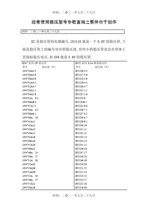
经常使用稳压型号参数查询之蔡仲巾千创作DZ是稳压管的电器编号,1N4148就是一个0.6V的稳压管,下面是稳压管上的编号对应的稳压值,有些小的稳压管也会在管体上直接标稳压电压,如5V6就是5.6V的稳压管.美标稳压二极管型号:HITACHI(日立):HITACHI(日立)0.5W稳压二极管型号参数稳压HZ3A1 2.5~2.7VHZ3A2 2.6~2.8VHZ3A3 2.6~2.9VHZ3B1 2.8~3.0VHZ3B2 2.9~3.1VHZ3B3 3.0~3.2V线性稳压器件(输入输出电流相等,压降3V以上)型号稳压(V) 最年夜输出电流可替代型号79L05 -5V 100mA79L06 -6V 100mA79L08 -8V 100mALM7805 5V 1A L7805,LM340T5LM7806 6V 1A L7806LM7808 8V 1A L7808LM7809 9V 1A L7809LM7812 12V 1A L7812,LM340T12LM7815 15V 1A L7815,LM340T15LM7818 18V 1A L7815LM7824 24V 1A L7824LM7905 -5V 1A L7905LM7906 -6V 1A L7906,KA7906LM7908 -8V 1A L7908LM7909 -9V 1A L7909LM7912 -12V 1A L7912LM7915 -15V 1A L7915LM7918 -18V 1A L7918LM7924 -24V 1A L792478L05 5V 100mA78L06 6V 100mA78L08 8V 100ma78L09 9V 100ma78L12 12V 100ma78L15 15V 100ma78L18 18V 100ma78L24 24V 100ma开关稳压器件(电压转换效率高)型号说明最年夜输出电流LM1575T-3.3 3.3V简易开关电源稳压器1ALM1575T-5.0 5V简易开关电源稳压器1ALM1575T-12 12V简易开关电源稳压器1ALM1575T-15 15V简易开关电源稳压器1ALM1575T-ADJ 简易开关电源稳压器(可调1.23V~37V) 1ALM1575HVT-3.3 3.3V简易开关电源稳压器1ALM1575HVT-5.0 5V简易开关电源稳压器1ALM1575HVT-12 12V简易开关电源稳压器1ALM1575HVT-15 15V简易开关电源稳压器1ALM1575HVT-ADJ 简易开关电源稳压器(可调1.23V~37V) 1ALM2575T-3.3 3.3V简易开关电源稳压器1ALM2575T-5.0 5V简易开关电源稳压器1ALM2575T-12 12V简易开关电源稳压器1ALM2575T-15 15V简易开关电源稳压器1ALM2575T-ADJ 简易开关电源稳压器(可调1.23V~ 37V) 1ALM2575HVT-3.3 3.3V简易开关电源稳压器1ALM2575HVT-5.0 5V简易开关电源稳压器1ALM2575HVT-12 12V简易开关电源稳压器1ALM2575HVT-15 15V简易开关电源稳压器1ALM2575HVT-ADJ 简易开关电源稳压器(可调1.23V~37V) 1ALM2576T-3.3 3.3V简易开关电源稳压器3ALM2576T-5.0 5.0V简易开关电源稳压器3ALM2576T-12 12V简易开关电源稳压器3ALM2576T-15 15V简易开关电源稳压器3ALM2576T-ADJ 简易开关电源稳压器(可调1.23V~37V) 3ALM2576HVT-3.3 3.3V简易开关电源稳压器3ALM2576HVT-5.0 5.0V简易开关电源稳压器3ALM2576HVT-12 12V简易开关电源稳压器3ALM2576HVT-15 15V简易开关电源稳压器3ALM2576HVT-ADJ 简易开关电源稳压器(可调1.23V~37V) 3A。
音响IC应用资料简要参数

4 Ohms 4 Ohms 4 Ohms 32 Ohms 4 Ohms 4 Ohms 4 Ohms 4 Ohms 4 Ohms 4 Ohms 4 Ohms 4 Ohms 4 Ohms 32 Ohms 4 Ohms 4 Ohms 8 Ohms 8 Ohms 4 Ohms 4 Ohms 4 Ohms 4 Ohms 4 Ohms 8 Ohms 8 Ohms 8 Ohms 4 Ohms 4 Ohms 4 Ohms 4 Ohms 4 Ohms 4 Ohms 4 Ohms 4 Ohms
+/-32V +/-35V +/-35V +/-30V
8 Ohms 8 Ohms 8 Ohms 4 Ohms
60W 70W 70W 30W 80W 35W
+/-38V +/-42V +/-42V +/-35V
8 Ohms 8 Ohms 8 Ohms 8 Ohms 4 Ohms 4 Ohms
+/-28.5V +/-25V
AN7171NK AN7173NK
AN7176 AN7177 AN7178 CXA1034PM HA13001 HA1377 HA1384 HA1388 HA1398 HA13108 K1075YH1 KA2211 KA2213 KA22135 KA2214 LA4101 LA4145 LA4162 LA4182 LA4183 LA4185 LA4190 LA4192 LA4261 LA4265 LA4282 LA4422 LA4440 LA4445 LA4446 LA4460N LA4461N LA4465 LA4475
16 Ohms 4 Ohms 4 Ohms 4 Ohms 4 Ohms
IC命名 封装 批号 常识等大全 IC基本认识

IC命名封装批号常识等大全IC基本认识德州仪器( TI ), 安森美( ON ), 国半( NSC ), 国半( NSC ),德意志半导体( STM ),恩智浦 (NXP ),欧司朗( OSRAM ),威世半导体( VISHAY ),英飞凌( INFINEON ),飞兆半导体( FAIRCHILD ),东芝( TOSHIBA )志半导体( STM ),恩智浦 (NXP ),欧司朗( OSRAM ),威世半导体( VISHAY ),英飞凌( INFINEON ),飞兆半导体( FAIRCHILD ),东芝( TOSHIBA )↑IC封装如上IC产品的命名规则:大部分IC产品型号的开头字母,也就是通常所说的前缀都是为生产厂家的前两个或前三个字母,比如:MA XIM公司的以MA X为前缀,AD公司的以A D为前缀,ATMEL公司的以A T为前缀,C Y公司的以C Y为前缀,像A MD,IDT,LT,DS,HY这些公司的IC产品型号都是以生产厂家的前两个或前三个为前缀。
但也有很生产厂家不是这样的,如TI的一般以SN,TMS,TPS,TL,TLC,TLV等字母为前缀;A LTERA(阿尔特拉)、XILINX(赛灵斯或称赛灵克斯)、Lattice(莱迪斯),称为可编程逻辑器件CPLD、FPGA。
A L TERA的以EP,EPM,EPF为前缀,它在亚洲国家卖得比较好,XILINX的以XC为前缀,它在欧洲国家卖得比较好,功能相当好。
Lattice一般以M4A,LSP,LSIG 为前缀,NS的以LM为前缀居多等等,这里就不一一做介绍了。
紧跟前缀后面的几位字母或数字一般表示其系列及功能,每个厂家规则都不一样,这里不做介绐,之后跟的几位字母(一般指的是尾缀)表示温度系数和管脚及封装,一般情况下,C表示民用级,I表示工业级,E表示扩展工业级,A表示航空级,M表示军品级下面几个介比较具有代表性的生产厂家,简单介绍一下:AMD公司F LASH常识:AM29L V 640 D(1)U(2)90R WH(3)I(4)1:表示工艺:B=0.32uM C=0.32uM thin-film D=0.23uM thin-film G=0.16uM thin-film M=MirrorBit2:表示扇区方式:T=TOP B=BOTTOM H=U nifom highest address L=U nifom low est address U、BL A NK=U nifom3:表示封装:P=PDIP J=PL CC S=SOP Z=SSOP E/F=TSSOP M/P/W=FPGA4:温度范围C=0℃TO+60℃I=-40℃TO+85℃E=-55TO℃+85℃MA XIMMA XIM产品命名信息(专有命名体系)MA XIM推出的专有产品数量在以下相当可观的速度增长.这些器件都按以功能划分的产品类别进行归类。
MEMORY存储芯片MT41J256M16RE-15EIT中文规格书

10.Release frame sync generators from reset.Note that it is necessary to release the internal frame syncgenerators from reset,even if an external frame sync is being used,because the frame sync errordetection logic is built into the frame sync generator.(a)Take the respective frame sync generator(s)out of reset by setting the RFRST bit for the receiver,and/or the XFRST bit for the transmitter in GBLCTL.All other bits in GBLCTL should be left at theprevious state.(b)Read back from GBLCTL to ensure the bit(s)to which you wrote are successfully latched inGBLCTL before you proceed.11.Upon the first frame sync signal,McASP transfers begin.The McASP synchronizes to an edge on theframe sync pin,not the level on the frame sync pin.This makes it easy to release the state machineand frame sync generators from reset.(a)For example,if you configure the McASP for a rising edge transmit frame sync,then you do notneed to wait for a low level on the frame sync pin before releasing the McASP transmitter statemachine and frame sync generators from reset.23.0.21.1.3Separate Transmit and Receive InitializationIn many cases,it is desirable to separately initialize the McASP transmitter and receiver.For example,you may delay the initialization of the transmitter until the type of data coming in on the receiver is recognized.Or a change in the incoming data stream on the receiver may necessitate a reinitialization of thetransmitter.In this case,you may still follow the sequence outlined in Section23.0.21.1.2,but use it for each section (transmit,receive)individually.The GBLCTL register is aliased to RGBLCTL and XGBLCTL to facilitate separate initialization of transmit and receive sections.Also,make sure that the initialization or reinitialization sequence follows the guidelines in Bits WithRestrictions on When They May be Changed.23.0.21.1.4Importance of Reading Back GBLCTLIn Section23.0.21.1.2,steps4b,5b,7c,9b,and10b state that GBLCTL should be read back until the bits that were written are successfully latched.This is important,because the transmitter and receiver state machines run off of the respective bit clocks,which are typically about tens to hundreds of times slower than the DSP's internal bus clock.Therefore,it takes many cycles between when the DSP writes toGBLCTL(or RGBLCTL and XGBLCTL),and when the McASP actually recognizes the write operation.If you skip this step,then the McASP may never see the reset bits in the global control registers getasserted and deasserted;resulting in an uninitialized McASP.Therefore,the logic in McASP has been implemented such that once the DSP writes GBLCTL,RGBLCTL, or XGBLCTL,the resulting write is not visible by reading back GBLCTL until the McASP has recognized the change.This typically requires two bit clocks plus two DSP bus clocks to occur.Also,if the bit clocks can be completely stopped,any software that polls GBLCTL should be implemented with a time-out.If GBLCTL does not have a time-out,and the bit clock stops,the changes written toGBLCTL will not be reflected until the bit clock restarts.Finally,please note that while RGBLCTL and XGBLCTL allow separate changing of the receive andtransmit halves of GBLCTL,they also immediately reflect the updated value(useful for debug purposes).Only GBLCTL can be used for the read back step.23.0.21.1.5Synchronous Transmit and Receive Operation(ASYNC=0)When ASYNC=0in ACLKXCTL,the transmit and receive sections operate synchronously from thetransmit section clock and transmit frame sync signals(Figure23-15).The receive section may have a different(but compatible in terms of slot size)data format.Note that when ASYNC=0,XCLK isautomatically inverted to produce RCLK(note the inversion on the ASYNC multiplexer as shown inFigure23-16).Table23-3.Channel Status and User Data for Each DIT BlockFrame Subframe Preamble Channel Status defined in:User Data defined in: Defined by DITCSRA0,DITCSRB0,DITUDRA0,DITUDRB001(L)B DITCSRA0[0]DITUDRA0[0]02(R)W DITCSRB0[0]DITUDRB0[0]11(L)M DITCSRA0[1]DITUDRA0[1]12(R)W DITCSRB0[1]DITUDRB0[1]21(L)M DITCSRA0[2]DITUDRA0[2]22(R)W DITCSRB0[2]DITUDRB0[2]……………311(L)M DITCSRA0[31]DITUDRA0[31]312(R)W DITCSRB0[31]DITUDRB0[31] Defined by DITCSRA1,DITCSRB1,DITUDRA1,DITUDRB1321(L)M DITCSRA1[0]DITUDRA1[0]322(R)W DITCSRB1[0]DITUDRB1[0]……………631(L)M DITCSRA1[31]DITUDRA1[31]632(R)W DITCSRB1[31]DITUDRB1[31] Defined by DITCSRA2,DITCSRB2,DITUDRA2,DITUDRB2641(L)M DITCSRA2[0]DITUDRA2[0]642(R)W DITCSRB2[0]DITUDRB2[0]……………951(L)M DITCSRA2[31]DITUDRA2[31]952(R)W DITCSRB2[31]DITUDRB2[31] Defined by DITCSRA3,DITCSRB3,DITUDRA3,DITUDRB3961(L)M DITCSRA3[0]DITUDRA3[0]962(R)W DITCSRB3[0]DITUDRB3[0]……………1271(L)M DITCSRA3[31]DITUDRA3[31]1272(R)W DITCSRB3[31]DITUDRB3[31] Defined by DITCSRA4,DITCSRB4,DITUDRA4,DITUDRB41281(L)M DITCSRA4[0]DITUDRA4[0]1282(R)W DITCSRB4[0]DITUDRB4[0]……………1591(L)M DITCSRA4[31]DITUDRA4[31]1592(R)W DITCSRB4[31]DITUDRB4[31] Defined by DITCSRA5,DITCSRB5,DITDRA5,DITUDRB51601(L)M DITCSRA5[0]DITUDRA5[0]1602(R)W DITCSRB5[0]DITUDRB5[0]……………1911(L)M DITCSRA5[31]DITUDRA5[31]1912(R)W DITCSRB5[31]DITUDRB5[31]。
俄罗斯电子元器件查找大全(2)
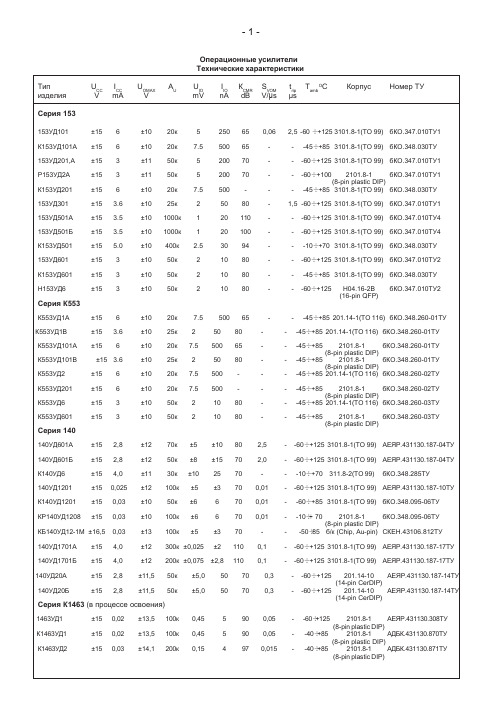
ОперационныеусилителиТехническиехарактеристикиТипUCC ICCUOMAXAUUIOIIОКCMRSVOMtripTambO CКорпусНомерТУизделияV mA V mV nA dB V/µsµsСерия 153153УД101±156±1020к5250650,062,5-60 ÷ +1253101.8-1(TO 99)бКО.347.010ТУ1К153УД101А±156±1020к7.550065---45÷ +853101.8-1(TO 99)бКО.348.030ТУ153УД201,A±153±1150к520070---60÷ +1253101.8-1(TO 99)бКО.347.010ТУ1Р153УД2А±153±1150к520070---60÷ +1002101.8-1бКО.347.010ТУ1(8-pin plastic DIP)К153УД201±156±1020к7.5500----45÷ +853101.8-1(TO 99)бКО.348.030ТУ153УД301±15 3.6±1025к25080-1,5-60÷ +1253101.8-1(TO 99)бКО.347.010ТУ1153УД501А±15 3.5±101000к120110---60÷ +1253101.8-1(TO 99)бКО.347.010ТУ4153УД501Б±15 3.5±101000к120100---60÷ +1253101.8-1(TO 99)бКО.347.010ТУ4К153УД501±15 5.0±10400к 2.53094---10÷ +703101.8-1(TO 99)бКО.348.030ТУ153УД601±153±1050к21080---60÷ +1253101.8-1(TO 99)бКО.347.010ТУ2К153УД601±153±1050к21080---45÷ +853101.8-1(TO 99)бКО.348.030ТУН153УД6±153±1050к21080---60÷ +125Н04.16-2ВбКО.347.010ТУ2(16-pin QFP)СерияК553К553УД1А±156±1020к7.550065---45÷ +85201.14-1(TO 116)бКО.348.260-01ТУК553УД1B±15 3.6±1025к25080---45÷ +85201.14-1(TO 116)бКО.348.260-01ТУК553УД101А±156±1020к7.550065---45÷ +852101.8-1бКО.348.260-01ТУ(8-pin plastic DIP)К553УД101B ±15 3.6±1025к25080---45÷ +852101.8-1бКО.348.260-01ТУ(8-pin plastic DIP)К553УД2±156±1020к7.5500----45÷ +85201.14-1(TO 116)бКО.348.260-02ТУК553УД201±156±1020к7.5500----45÷ +852101.8-1бКО.348.260-02ТУ(8-pin plastic DIP)К553УД6±153±1050к21080---45÷ +85201.14-1(TO 116)бКО.348.260-03ТУК553УД601±153±1050к21080---45÷ +852101.8-1бКО.348.260-03ТУ(8-pin plastic DIP)Серия 140140УД601А±152,8±1270к±5±10802,5--60÷ +1253101.8-1(TO 99)АЕЯР.431130.187-04ТУ140УД601Б±152,8±1250к±8±15702,0--60÷ +1253101.8-1(TO 99)АЕЯР.431130.187-04ТУК140УД6±154,0±1130к±102570---10÷ +70311.8-2(TO 99)бКО.348.285ТУ140УД1201±15 0,025±12100к ±5±3700,01--60÷ +1253101.8-1(TO 99)АЕЯР.431130.187-10ТУК140УД1201±15 0,03±1050к±66700,01--60÷ +853101.8-1(TO 99)бКО.348.095-06ТУКР140УД1208±15 0,03±10100к ±66700,01--10÷+ 702101.8-1бКО.348.095-06ТУ(8-pin plastic DIP)КБ140УД12-1М±16,5 0,03±13100к ±5±370---50÷85б/к (Chip, Au-pin)СКЕН.43106.812ТУ140УД1701А±154,0±12300к±0,025±21100,1--60÷ +1253101.8-1(ТО 99)АЕЯР.431130.187-17ТУ140УД1701Б±154,0±12200к±0,075±2,81100,1--60÷ +1253101.8-1(ТО 99)АЕЯР.431130.187-17ТУ140УД20А±152,8±11,550к±5,050700,3--60÷ +125201.14-10АЕЯР.431130.187-14ТУ(14-pin CerDIP)140УД20Б±152,8±11,550к±5,050700,3--60÷ +125201.14-10АЕЯР.431130.187-14ТУ(14-pin CerDIP)СерияК1463 (впроцессеосвоения)1463УД1±150,02±13,5100к0,455900,05--60÷+1252101.8-1АЕЯР.431130.308ТУ(8-pin plastic DIP)К1463УД1±150,02±13,5100к0,455900,05--40÷+852101.8-1АДБК.431130.870ТУ(8-pin plastic DIP)К1463УД2±150,03±14,1200к0,154970,015--40÷+852101.8-1АДБК.431130.871ТУ(8-pin plastic DIP)- 1 -ТипUCC ICCUOMAXAUUIOIIОКCMRSVOMtripTambO CКорпусНомерТУизделияV mA V mV nA dB V/µsµs1463УД3±156,8±1250к1500100230--60÷+1252101.8-1АЕЯР.431130.309ТУ(8-pin plastic DIP)К1463УД3±156,8±1250к1500100230--40÷+852101.8-1АДБК.431130.872ТУ(8-pin plastic DIP)1463УБ1±151,3±13,6 1÷1k 0,125173÷110---60÷+1252101.8-1АЕЯР.431130.307ТУ(8-pin plastic DIP)К1463УБ1±151,3±13,6 1÷1k 0,125173÷110---40÷+852101.8-1АДБК.431130.873ТУ(8-pin plastic DIP)AS301АN±153±1025к7.55070--0÷+ 702101.8-1ЩТ3.423.010-05ТУ(8-pin plastic DIP)КР1401УД2+32 3.0+2625k7.05066--0÷ +70201.14-1(TO 116)бКО.348.651ТУ/02счетверенныйAS324N+32 3.0+2625k7.05066--0÷ +70201.14-1(TO 116)СКЕН.431136.808ТУсчетверенныйAS2902N+32 3.0+2625k7.05066---45÷ +85201.14-1(TO 116)СКЕН.431136.808ТУсчетверенныйК1040УД1+32 2.0+2625k7.05066--0÷ +702101.8-1бКО.349.078ТУсдвоенный(8-pin plastic DIP)AS358N+32 2.0+2625k7.05066--0÷ +702101.8-1ЩТ3.423.010-03ТУсдвоенный(8-pin plastic DIP)AS258N+32 2.0+2625k7.05066---45÷ +852101.8-1ЩТ3.423.010-03ТУсдвоенный(8-pin plastic DIP)Серия 740140УД6АН1АР±152,8±1270к±5±10802,5--60÷ +100б/к (Chip, Au-pin)АЕЯР.431130.216ТУ(740УД4-1 стар. обоз.)140УД6БН1АР±152,8±1250к±8±15802,0--60÷ +100б/к (Chip, Au-pin)АЕЯР.431130.216ТУ(740УД4-1 стар. обоз.)- 2 -Компараторынапряжения.ТипUcc1Ucc2UCC3ICC1ICC2ICC3UIOIIОtDLHTambO CКорпусНомерТУизделияV V V mA mA mA mV nA ncСерия 521521СА10112-6-11.5 6.5- 3.510к110-60÷ +1253107.12-1 (TO 100)бКО.347.015 ТУ1сдвоенныйК521СА10112-6-11.5 6.5-7.510к120-45÷ +853107.12-1 (TO 100)бКО.348.279-01 ТУсдвоенный521СА20112-6-98-510к120-60÷ +1253101.8-1 (TO 99)бКО.347.015 ТУ1Б521СА2-212-6-98-510к120-60÷ +100б/кбКО.347.454-01ТУ(Chip, Polyim. film)К521СА20112-6-98-7.510к120-45÷ +853101.8-1 (TO 99)бКО.348.279-01 ТУ 521СА30115-15-65-310300-60÷ +1253101.8-1 (TO 99)бКО.347.015 ТУ2Б521СА3-115-15-65-310300-60÷ +100б/к (Chip, Au-pin)бКО.347.115ТУ2Б521СА3-215-15-65-310300-60÷ +100б/кбКО.347.454-02ТУ(Chip, Polyim. film)Н521СА315-15-65-310300-60÷ +125Н04.16-2ВбКО.347.015 ТУ2(16-pin QFP)К521СА301А15-15-65-310300-45÷ +853101.8-1 (TO 99)бКО.348.279-02 ТУК521СА301Б15-15-7,55-7.550300-45÷ +853101.8-1 (TO 99)бКО.348.279-02 ТУ521СА4019.0-9.0 5.0 3.757.51640.5к26-60÷ +1253107.12-1 (TO 100)бКО.347.015 ТУ3Б521СА4-19.0-9.0 5.0 3.757.51640.5к26-60÷ +100б/к (Chip, Au-pin)бКО.347.115-03ТУК521СА4019.0-9.0 5.0 4.08.51850.75к26-45÷ +853107.12-1 (TO 100)бКО.348.279-03 ТУК521СА60112-12 5.012.55-40.2к150-10÷ +703107.12-1НБбКО.348.279-04 ТУсдвоенный(TO 100)СерияР(К)554К554СА20112-6-98-7.510к120-45÷ +852101.8-1бКО.348.279-01 ТУ(8-pin plastic DIP)К554СА301А15-15-65-310300-45÷ +852101.8-1бКО.348.279-02 ТУ(8-pin plastic DIP)AS211N15-15-65-310300-25÷ +852101.8-1ЩТ3.423.010-06 ТУ(8-pin plastic DIP)К554СА301Б15-15-65-7.510300-45÷ +852101.8-1бКО.348.279-02ТУ(8-pin plastic DIP)AS311N15-15-7.55-7.5503000÷ +702101.8-1ЩТ3.423.010-06 ТУ(8-pin plastic DIP)Р554СА212-6-98-510к120-60÷ +1002101.8-1бКО.347.473-01 ТУ(8-pin plastic DIP)Р554СА3А15-15-65-310300-60÷ +1002101.8-1бКО.347.473-02 ТУ(8-pin plastic DIP)К554СА112-6-11.5 6.5-7.510к120-45÷ +85201.14-1(TO 116)бКО.348.279-01 ТУсдвоенныйК554СА2126-98-7.510к120-45÷ +85201.14-1(TO 116)бКО.348.279-01 ТУК554СА3А1515-65-310300-45÷ +85201.14-1(TO 116)бКО.348.279-02 ТУК554СА3Б1515-7,55-7.510300-45÷ +85201.14-1(TO 116)бКО.348.279-02 ТУК554СА49.09.0 5.0 4.08.51850.75к26-45÷ +85201.14-1(TO 116)бКО.348.279-03ТAS339N1818- 2.5-- 5.0503000÷ +70201.14-1(TO 116)СКЕН 431136.808-01ТУсчетверенныйКР1401СА1Б1818- 2.5-- 5.0503000÷ +70201.14-1(TO 116)И63.487.024-18ТУКР1040СА11818- 2.5-- 5.0503000÷ +702101.8-1бКО.349.080ТУсдвоенный(8-pin plastic DIP)AS393N1818- 2.5-- 5.0503000÷ +702101.8-1ЩТ3.423.010-04ТУсдвоенный(8-pin plastic DIP)AS3V3933--0,02--50,325000÷ +702101.8-1ЩТ3.423.010-07ТУ(8-pin plastic DIP)597СА3АТАР151552,61-5350300-60÷ +100402.16-33АЕЯР431350.353ТУсдвоенный597СА3БТАР151552,61-5350370-60÷ +100402.16-33АЕЯР431350.353ТУсдвоенный597СА3АУАР151552,61-5350300-60÷ +100H04.18-2BАЕЯР431350.353ТУсдвоенный597СА3БУАР151552,61-5350370-60÷ +100H04.18-2BАЕЯР431350.353ТУсдвоенныйЦифро-аналоговыепреобразователи.ТипRes tS DNL INLδFS Ucc Icc UREFIoutInputs TambO CКорпусНомерТУизделияbitsµs%%% from FS V mA V mA ViL /VihСерия 572572ПА1А1050,10,1-3÷0,5152±10.24-0.8/3.6-60÷+85201.16-8бКО. 347.182ТУ1(16-pin CerDIP)572ПА1Б1050,20,2-3÷0,5152± 10.24-0.8/3.6-60÷+85201.16-8бКО. 347.182ТУ1(16-pin CerDIP)572ПА1В1050,40,4-3÷0,5152± 10.24-0.8/3.6-60÷+85201.16-8бКО. 347.182ТУ1(16-pin CerDIP)Р572ПА1А1050,10,1-3÷0,5152± 10.24-0.8/3.6-60÷+85238.16-1бКО. 347.182ТУ1(16-pin PlasticDIP)Р572ПА1Б1050,20,2-3÷0,5152± 10.24-0.8/3.6-60÷+85238.16-1бКО. 347.182ТУ1(16-pin PlasticDIP)Р572ПА1В1050,40,4-3÷0,5152± 10.24-0.8/3.6-60÷+85238.16-1бКО. 347.182ТУ1(16-pin PlasticDIP)Н572ПА1A1050,10,1-3÷0,5152±10.24-0.8/3.6-60÷+85Н04.16-1ВбКО. 347.182ТУ1(16-pin QFP)Н572ПА1Б1050,20,2-3÷0,5152±10.24-0.8/3.6-60÷+85Н04.16-1ВбКО. 347.182ТУ1(16-pin QFP)Н572ПА1В1050,40,4-3÷0,5152±10.24-0.8/3.6-60÷+85Н04.16-1ВбКО. 347.182ТУ1(16-pin QFP)Б572ПА1-11050,10,13152± 10.24-0.8/3.6-60÷+85б/кРАЕ-012.ПА1(Chip, Au-pin)К572ПА1А1050,10,13152±10.24-0.8/3.6-10÷+70201.16-8бКО.348.432-01ТУ(16-pin CerDIP)К572ПА1Б1050,20,23152± 10.24-0.8/3.6-10÷+70201.16-8бКО.348.432-01ТУ(16-pin CerDIP)КР572ПА1А1050,10,13152± 10.24-0.8/3.6-10÷+70238.16-1бКО.348.432-01ТУ(16-pin PlasticDIP)КР572ПА1Б1050,20,23152± 10.24-0.8/3.6-10÷+70238.16-1бКО.348.432-01ТУ(16-pin PlasticDIP)AS7533LN100.6±0,05±0,051.4172±25-0.8/2.4-40÷+85238.16-1ЩТ3.430.000-02ТУ(16-pin PlasticDIP)AS7533KN100.6±0,1±0,11.4172±25-0.8/2.4-40÷+85238.16-1ЩТ3.430.000-02ТУ(16-pin PlasticDIP)572ПА2А12100,10,10.15/151.510.24-TTL-60÷+854134.48-2бКО.347.182ТУ2(48-pin Cer Flatpack)572ПА2 Б12100,20,20.35/151.510.24-TTL-60÷+854134.48-2бКО.347.182ТУ2(48-pin Cer Flatpack)К572ПА2А1215±0,025±0,0250.55/15 2.010.24-TTL-10÷+704134.48-2бКО. 348.432-02ТУ(48-pin Cer Flatpack)К572ПА2Б1215±0,05±0,050.55/15 2.010.24-TTL-10÷+704134.48-2бКО. 348.432-02ТУ(48-pin Cer Flatpack)К572ПА2B1215±0,1±0,10.55/15 2.010.24-TTL-10÷+704134.48-2бКО. 348.432-02ТУ(48-pin Cer Flatpack)КР572ПА2А1215±0,025±0,0250.55/15 2.010.24-TTL-10÷+702123.40-2бКО. 348.432-02ТУ(40-pin Plastic DIP)КР572ПА2Б1215±0,05±0,050.55/15 2.010.24-TTL-10÷+702123.40-2бКО. 348.432-02ТУ(40-pin Plastic DIP)КР572ПА2B1215±0,1±0,10.55/15 2.010.24-TTL-10÷+702123.40-2бКО. 348.432-02ТУ(40-pin Plastic DIP)Серия11081108ПА1А120.4±0,018±0,0180.245/-1515/4810.243-7TTL-60÷+85210Б.24-1бКО.347.347-01ТУ(24-pin CerDIP)1108ПА1Б120.4±0,048±0,0480.55/-1515/4810.243-7TTL-60÷+85210Б.24-1бКО.347.347-01ТУ(24-pin CerDIP)К1108ПА1А120.4±0,024±0,0240.35/-1515/4610.243-7TTL-10÷+70210Б.24-1бКО.348.645-ТУ(24-pin CerDIP)К1108ПА1Б120.7±0,024±0,0240.35/-1515/4610.243-7TTL-10÷+70210Б.24-1бКО.348.645-ТУ(24-pin CerDIP)Н1108ПА1А120.4±0,018±0,0180.245/-1515/4810.243-7TTL-60÷+85Н14.42-2ВбКО.347.347-01ТУ(42-pin QFP)Н1108ПА1Б120.4±0,048±0,0480.245/-1515/4810.243-7TTL-60÷+85Н14.42-2ВбКО.347.347-01ТУ(42-pin QFP)Н1108ПА281.0±0,2±0,21.55/-640/50int 2.5TTL-45÷+85238.18-1бКО.347.347-04ТУ(18-pin CerDIP )Радар-Т120.12±0,018±0,0180.245/-1515/4810.243-7TTL-60÷+85210Б.24-1ОКРвстадии(24-pin CerDIP)разработкиАналого-цифровыепреобразователи.ТипRes tСDNL INLδFS UCCICCUREFUINTambO CКорпусНомерТУизделияbitsµs±LSB±LSB±LSB V mA V VСерия 572572ПВ1А1215010.75105/+151.0/1.5± 10.2410-60÷+854134.48-2бКО.347.182-03ТУ(48-pin CerFlatpack)572ПВ1Б1215042405/+151.0/1.5± 10.2410-60÷+854134.48-2бКО.347.182-03ТУ(48-pin CerFlatpack)К572ПВ1А12150421225/+153/5± 10.2410-10÷+704134.48-2бКО.348.432-03ТУ(48-pin CerFlatpack)К572ПВ1Б12150841225/+153/5± 10.2410-10÷+704134.48-2бКО.348.432-03ТУ(48-pin CerFlatpack)К572ПВ1В1215011105/+153/5± 10.2410-10÷+704134.48-2бКО.348.432-03ТУ(48-pin CerFlatpack)КР572ПВ1А12150421225/+153/5± 10.2410-10÷+702123.40-2бКО.348.432-03ТУ(40-pin Plastic DIP)КР572ПВ1Б12150841225/+153/5± 10.2410-10÷+702123.40-2бКО.348.432-03ТУ(40-pin Plastic DIP)КР572ПВ1В1215011105/+153/5± 10.2410-10÷+702123.40-2бКО.348.432-03ТУ(40-pin Plastic DIP)КР572ПВ2А 3.5dec.-11-5/-51.81.02-10÷+702123.40-2бКО.348.432-04ТУ(40-pin Plastic DIP)КР572ПВ2Б 3.5dec.-33-5/-51.81.02-10÷+702123.40-2бКО.348.432-04ТУ(40-pin Plastic DIP)КР572ПВ2В 3.5dec.-55-5/-51.81.02-10÷+702123.40-2бКО.348.432-04ТУ(40-pin Plastic DIP)Н572ПВ387.50.750.535 2.5-1010-60÷+125H09.18-1BбКО.347.182-05ТУ(18-pin QFP)КР572ПВ387.50,750.535 2.5-1010-10÷+70238.18-3бКО.348.432-08ТУ(18-pin Plastic DIP)К572ПВ48250.50.515 3.0±2.5±2.5-25÷+852121.28-6бКО.348.432-05ТУ(24-pin CerDIP)КР572ПВ5 3.5dec.-11191.81.0±1,9-10÷+702123.40-2бКО.348.412-07ТУ(40-pin Plastic DIP)Серия11081108ПВ1А100.90.75145/-5.250/130 2.5/in. 2.8-45÷+85210.Б.24-1бКО.347.347-02ТУ(24-pin CerDIP)1108ПВ1Б100.93375/-5.250/130 2.5/in. 2.8-45÷+85210.Б.24-1бКО.347.347-02ТУ(24-pin CerDIP)1108ПВ1Г100.90.75145/-5.250/130 2.5/in. 2.8-25÷+70210.Б.24-1бКО.347.347-02ТУ(24-pin CerDIP)К1108ПВ1А100.90.75145/-5.250/130 2.5/in. 2.8-10÷+70210.Б.24-1бКО.348.863-ТУ(24-pin CerDIP)К1108ПВ1Б100.93375/-5.250/130 2.5/in. 2.8-10÷+70210.Б.24-1бКО.348.863-ТУ(24-pin CerDIP)Н1108ПВ1А100.90.75145/-5.250/130 2.5/in. 2.8-45÷+85H14.42-1BбКО.347.347-02ТУ(42-pin QFP)Н1108ПВ1Б100.93375/-5.250/130 2.5/in. 2.8-45÷+85H14.42-1BбКО.347.347-02ТУ(42-pin QFP)Н1108ПВ1Г100.90.75145/-5.250/130 2.5/in. 2.8-25÷+70H14.42-1BбКО.347.347-02ТУ(42-pin QFP)1108ПВ212 2.01.0 2.0105/-680/150 2.5/in.5/±2.5-45÷+852123.40-6бКО.347.347-05ТУ(40-pin CerDIP)К1108ПВ212 2.01.0 2.0105/-680/150 2.5/in.5/±2.5-10÷+702123.40-6бКО.348.863-ТУ(40-pin CerDIP)Серия11131113ПВ1А10301155/-1510/18int.10/±5-45÷+85238.18-1бКО.347.365-01ТУ(18-pin CerDIP)1113ПВ1Б103042105/-1510/18int.10/±5-45÷+85238.18-1бКО.347.365-01ТУ(18-pin CerDIP)1113ПВ1В103042105/-1510/18int.10/±5-60÷+125238.18-1бКО.347.365-01ТУ(18-pin CerDIP)1113ПВ1Г10301155/-1510/18int.10/±5-45÷+85238.18-1бКО.347.365-01ТУ(18-pin CerDIP)К1113ПВ1А10301145/-1510/18int.10/±5-10÷+70238.18-1бКО.348.636-ТУ(18-pin CerDIP)К1113ПВ1Б10302245/-1510/18int.10/±5-10÷+70238.18-1бКО.348.636-ТУ(18-pin CerDIP)К1113ПВ1В10304445/-1510/18int.10/±5-10÷+70238.18-1бКО.348.636-ТУ(18-pin CerDIP)К1113ПВ1Г10304445/-1510/18int.10/±5-10÷+70238.18-1бКО.348.636-ТУПреобразователинапряжение-частота, частота-напряжение.ТипUio Iio1Iio2δLUFδLFUδFS UCC ICCTambO CКорпусНомерТУизделияmV nA nA x 10-6x 10⁻⁶% from FS V mAКР1108ПП1±4±150±60100100±1015/-156/6-10÷+70201.14-1(ТО116)бКО.348.758ТУКР1108ПП1±4±150±60100100±1015/-156/6-10÷+70201.14-1(ТО116)бКО.348.758ТУ1108ПП1±4±150±60100100±1015/-156/6-60÷+85201.14-10бКО.347.347-03ТУ(14-pin CerDIP)Р1108ПП1±4±150±60100100±1015/-156/6-60÷+85201.14-1(ТО116)бКО.347.347-03ТУК1108ПП1±4±150±60100100±1015/-156/6-10÷+70201.14-10бКО.348.758ТУТаймерыТипUCC IOICCδTambO CКорпусНомерТУизделияV mA mA/15V%Серия1006Р1006ВИ15-15100122-60÷+100201.14-1(TO 116)бКО.347.395-01ТУМ1006ВИ15-15100122-60÷+125201.14-10бКО.347.395-01ТУ(14-pin CerDIP)КР1006ВИ15-15100153-45÷+ 702101.8-1бКО.348.685 ТУAS555CN4,5-16,51001530÷+702101.8-1ТУЛР 000308466-10-93(8-pin plastic DIP)AS556CN4,5-16,51002830÷+70201.14-1(TO 116)СКЕН431136.808-02ТУсдвоенныйAS7555IPA2-181000.255-20÷+852101.8-1ЩТ3.423.010 ТУ(8-pin plastic DIP)КР1441ВИ12-181000.253-20÷+852101.8-1АДБК.431280.421ТУ(8-pin plastic DIP)Регуляторы напряженияТипТехническая характеристикаT amb O CКорпусНомер ТУизделияAS78LXXCP3-Terminal Positive Regulators V O (5,6,8,9,12,15)V;0÷+70КТ 26(ТО 92)СКЕН.431422.800 ТУV IN MAX 35V; δV O ±10%; I OMAX =100mAКР1157ЕНXX01Б3-Terminal Positive Regulators V O (5,6,8,9,12,15)V;0÷+70КТ 26(ТО 92)АДБК.431420.049ТУV IN MAX 35V; δV O ±10%; I OMAX =100mAAS78LXXAC Р3-Terminal Positive Regulators V O (5,6,8,9,12,15)V;0÷+70КТ 26(ТО 92)СКЕН.431422.800 ТУV IN MAX 35V; δV O ±5%; I OMAX =100mAКР1157ЕНXX01А3-Terminal Positive Regulators V O (5,6,8,9,12,15)V;0÷+70КТ 26(ТО 92)АДБК.431420.049ТУV IN MAX 35V; δV O ±5%; I OMAX =100mAAS79LXXCP 3-Terminal Negative Regulators V O (5,6,8,9,12,15)V;0÷+70КТ 26(ТО 92)СКЕН.431422.801 ТУV IN MAX 35V; δV O ±10%; I OMAX =100mAКР1168ЕНXX Б3-Terminal Negative Regulators V O (5,6,8,9,12,15)V;0÷+70КТ 26(ТО 92)АДБК.431420.198ТУV IN MAX 35V; δV O ±10%; I OMAX =100mAAS79LXXACP 3-Terminal Negative Regulators V O (5,6,8,9,12,15)V;0÷+70КТ 26(ТО 92)СКЕН.431422.801 ТУV IN MAX 35V; δV O ±5%; I OMAX =100mAКР1168ЕНXX А3-Terminal Negative Regulators V O (5,6,8,9,12,15)V;0÷+70КТ 26(ТО 92)АДБК.431420.198ТУV IN MAX 35V; δV O ±5%; I OMAX =100mAAS317L 3-Terminal Adjustable Regulators V O 1,2V ÷ 37,0V; I OMAX =100mA0÷+70КТ 26(ТО 92)СКЕН.431422.802 ТУAS385-2,5Micropower Voltage Reference V O =+ 2,5V ; I OMAX =20mA-10÷+70КТ 26(ТО 92)СКЕН.431422.803 ТУЗаказныеаналого-цифровыемикросхемыТипизделия UCC (V)ICC(mA)TambO CКорпусEuro 1-54,5-5,50,01-40 +85PLCC84(84-pin plastic) AS290-H1,5-16,50,055-65÷+85H04.16-1BASXP193P8-1810-45÷+852101.8-1(8-pin plastic DIP) ASXP194P8-186-45÷+85201.14-1(TO 116) ASXP195P8,50,2-45÷+852101.8-1(8-pin plastic DIP) ASXP642P1618-45÷+852101.8-1(8-pin plastic DIP) LMS 1118,55-45÷+85238.18-1(18-pin plastic DIP) VAC 3308,53-45÷+852101.18-1(18-pin plastic DIP) CT 7073143-45÷+852101.16-1(16-pin plastic DIP) AS194H3520-60 +1253101.8-1(TO-99)LC3608,51,0-45 +852101.8-1(8-pin plastic DIP) MT420 5 - 155-45 +85SOIC 24(24-pin plastic) LCD10418,50,2-45÷+85 SOIC 32Транзисторныепары (p-n-p).ТипFT Pcmax UCEOICh21EUCE satTSF h21ETambO CКорпусНомерТУизделияMHz mW V mA V ns dB½Транзисторныепары (p-n-p)2ТС3103А 600300152040-2000.6--0.9-60÷+1253101.8-1(TO 99)aAO.339.031 TУ2ТС3103Б 600300152040-2000.6--0.8-60÷+1253101.8-1(TO 99)aAO.339.031 TУКТC3103А 600300152040-2000.6--0.9-45÷+853101.8-1(TO 99)aAO.336.221 TУКТC3103Б 600300152040-2000.6--0.8-45÷+853101.8-1(TO 99)aAO.336.221 TУКТC3103А1 600300152040-2000.6--0.9 -45÷+85 2101.8-1aAO.336.221 TУ(8-pin plastic DIP)КТC3103Б1 600300152040-2000.6--0.8-45÷+85 2101.8-1aAO.336.221 TУ(8-pin plastic DIP)2ТС393А-1 50020101040-1800.6--0.9 -60÷+85б/к (Chip, Au-pin)ХМ3.363.000ТУ2ТС393Б-1 50020151030-140 ---0.8 -60÷+85б/к (Chip, Au-pin)ХМ3.363.000ТУКТС393А-1 50020101040-1800.6--0.9-45÷+85б/к (Chip, Au-pin)аА0.336.099ТУКТС393Б-1 50020151030-140---0.8-45÷+85б/к (Chip, Au-pin)аА0.336.099ТУТранзисторы (p-n-p)ТипFT Pcmax UCEOICh21EUCE satTSF h21ETambO CКорпусНомерТУизделияMHz mW V mA V ns dB½2Т363А1000150153020-1200.3510---60÷+125КТ-1-7(ТО 18)ЩТО.336.008ТУ2Т363Б1500150123040-1200.355---60÷+125КТ-1-7(ТО 18)ЩТО.336.008ТУКТ363А1000200153020-1200.3510---45÷+85КТ-1-7(ТО 18)ЩТО.336.014ТУКТ363Б1500200123040-1200.355---45÷+85КТ-1-7(ТО 18)ЩТО.336.014ТУКТ363АМ1000200153020-1200.3510---45÷+85КТ-26(ТО 92)ЩТО.336.014ТУКТ363БМ1500200123040-1200.355---45÷+85КТ-26(ТО 92)ЩТО.336.014ТУКТ326А400200155020-700,30----60÷+125КТ-1-7(ТО 18)аАО.336.196ТУКТ326Б400200155045-1600,30----60÷+125КТ-1-7(ТО 18)аАО.336.196ТУКТ639А80100045150040-1000.5----60÷+125КТ-27-2(ТО 126)аАО.336.267ТУКТ639Б80100045150063-1600.5----60÷+125КТ-27-2(ТО 126)аАО.336.267ТУКТ639В801000451500100-2500.5----60÷+125КТ-27-2(ТО 126)аАО.336.267ТУКТ639Г80100060150040-1000.5----60÷+125КТ-27-2(ТО 126)аАО.336.267ТУКТ639Д80100060150063-1600.5----60÷+125КТ-27-2(ТО 126)аАО.336.267ТУКТ639Е80100080150040-1000.5----60÷+125КТ-27-2(ТО 126)аАО.336.267ТУКТ639 Ж80100080150063-1600.5----60÷+125КТ-27-2(ТО 126)аАО.336.267ТУКТ639И801000301500180-4000.5----60÷+125КТ-27-2(ТО 126)аАО.336.267ТУКТ644А20010006060040-1200.4180---60÷+125КТ-27-2(ТО 126)аАО.336.268ТУКТ644Б200100060600100-3000.4180---60÷+125КТ-27-2(ТО 126)аАО.336.268ТУКТ644В20010004060040-1200.4180---60÷+125КТ-27-2(ТО 126)аАО.336.268ТУКТ644Г200100040600100-3000.4180---60÷+125КТ-27-2(ТО 126)аАО.336.268ТУКТ668А2005004510075-1400.3-10/1kHz--60÷+125КТ-26(TO 92)aAO.336.717 TУКТ668Б20050045100125-2500.3-10/1kHz--60÷+125КТ-26(TO 92)aAO.336.717 TУКТ668В20050045100220-4750.3-10/1kHz--60÷+125КТ-26(TO 92)aAO.336.717 TУКТ684А4080045100040-2500.5---- 45÷+125КТ-26(TO 92)aAO.336.806 TУКТ684Б4080060100040-1600.5---- 45÷+125КТ-26(TO 92)aAO.336.806 TУКТ684В4080080100040-1600.5---- 45÷+125КТ-26(TO 92)aAO.336.806 TУКТ684Г80800 -1500180-4000.5---- 45÷+125КТ-26(TO 92)aAO.336.806 TУКТ685А2006004060040-1200.480---60÷+125КТ-26(TO 92)aAO.336.810 TУКТ685Б2006006060040-1200.480---60÷+125КТ-26(TO 92)aAO.336.810 TУКТ685В20060040600100-3000.480---60÷+125КТ-26(TO 92)aAO.336.810 TУКТ685Г20060060600100-3000.480---60÷+125КТ-26(TO 92)aAO.336.810 TУКТ685Д3506002560070-2000.380---60÷+125КТ-26(TO 92)aAO.336.810 TУКТ685Е2506002560040-1200.3150---60÷+125КТ-26(TO 92)aAO.336.810 TУКТ685Ж25060025600100-3000.3150---60÷+125КТ-26(TO 92)aAO.336.810 TУКТ686А10062545800100-2500.7----60÷+125КТ-26(TO 92)aAO.336.814 TУКТ686Б10062545800160-4000.7----60÷+125КТ-26(TO 92)aAO.336.814 TУКТ686В10062545800250-6300.7----60÷+125КТ-26(TO 92)aAO.336.814 TУКТ686Г10062525800100-2500.7----60÷+125КТ-26(TO 92)aAO.336.814 TУКТ686 Д10062525800160-4000.7----60÷+125КТ-26(TO 92)aAO.336.814 TУКТ686Е10062525800250-6300.7----60÷+125КТ-26(TO 92)aAO.336.814 TУТипFT Pcmax UCEOICh21EUCE satTSF h21ETambO CКорпусНомерТУизделияMHz mW V mA V ns dB½КТ686Ж10062525800100-2500.7----60÷+125КТ-26(TO 92)aAO.336.814 TУКТ3107А2503004510070-1400.2-10/1kHz--60÷+125КТ-26(TO 92)aAO.336.170 TУКТ3107Б25030045100120-2200.2-10/1kHz--60÷+125КТ-26(TO 92)aAO.336.170 TУКТ3107В 2503002510070-1400.2-10/1kHz--60÷+125КТ-26(TO 92)aAO.336.170 TУКТ3107Г 25030025100120-2200.2-10/1kHz--60÷+125КТ-26(TO 92)aAO.336.170 TУКТ3107 Д 25030025100180-4600.2-10/1kHz--60÷+125КТ-26(TO 92)aAO.336.170 TУКТ3107Е 25030020100120-2200.2-4/1kHz--60÷+125КТ-26(TO 92)aAO.336.170 TУКТ3107Ж 25030020100180-4600.2-4/1kHz--60÷+125КТ-26(TO 92)aAO.336.170 TУКТ3107И 25030045100180-4600.2-10/1kHz--60÷+125КТ-26(TO 92)aAO.336.170 TУКТ3107К 25030025100380-8000.2-10/1kHz--60÷+125КТ-26(TO 92)aAO.336.170 TУКТ3107Л 25030020100380-8000.2-4/1kHz--60÷+125КТ-26(TO 92)aAO.336.170 TУ2T3108А 2503006020050-1500.251756/100MHz--60÷+125КТ-1-7(TO 18)aAO.339.026 TУ2T3108Б 2503004520050-1500.251756/100MHz--60÷+125КТ-1-7(TO 18)aAO.339.026 TУ2T3108В 30030045200100-3000.25-6/100MHz--60÷+125КТ-1-7(TO 18)aAO.339.026 TУ 2T3108 А1 2503006020050-1500.251756/100MHz--60÷+125КТ-26(TO 92)aAO.339.026 ТУ2T3108Б1 2503004520050-1500.251756/100MHz--60÷+125КТ-26(TO 92)aAO.339.026 TУ2T3108В1 30030045200100-3000.25-6/100MHz--60÷+125КТ-26(TO 92)aAO.339.026 TУКТ3109А 1100170255020--6/800MHz--45÷+85KT-29(TO 50)aAO.336.220 TУКТ3109A1 1100170255020--6/800MHz--45÷+85KT-29(TO 92)aAO.336.220 TУ2Т360А-1 30010202025-700.35 ----60÷+85б/к (Chip, Au-pin)ЩТ3.365.059ТУ2Т360Б-1 40010152040-1200.35 ----60÷+85б/к (Chip, Au-pin)ЩТ3.365.059ТУ2Т360В-1 40010152080-2400.35----60÷+85б/к (Chip, Au-pin)ЩТ3.365.059ТУ2Т364А-2 250302020020-700.3100---60÷+85б/к (Chip, Au-pin)ЩТ3.365.060ТУ2Т364Б-2 250302020040-1200.3130---60÷+85б/к (Chip, Au-pin)ЩТ3.365.060ТУ2Т364В-2 250302020080-2400.3160---60÷+85б/к (Chip, Au-pin)ЩТ3.365.060ТУКТ364А-2 250302020020-700.3150---45÷+85б/к (Chip, Au-pin)ЩТ0.336.011ТУКТ364Б-2 250302020040-1200.3180---45÷+85б/к (Chip, Au-pin)ЩТ0.336.011ТУКТ364В-2 250302020080-2400.3230---45÷+85б/к (Chip, Au-pin)ЩТ0.336.011ТУ2Т370А-1 10001515 1520-700.3510---60÷+85б/к (Chip, Au-pin)ЩТ3.365.067ТУ2Т370Б-1 12001512 1540-1200.3510---60÷+85б/к (Chip, Au-pin)ЩТ3.365.067ТУКТ370А-1 100015153020-700.3510---45÷+85б/к (Chip, Au-pin) aAO.336.005ТУКТ370Б-1 120015123040-1200.3510---45÷+85б/к (Chip, Au-pin) aAO.336.005ТУ2Т392А-2 300120401040-180---- -60÷+85б/к (Chip, Au-pin)ХМ3.365.022ТУ2Т3123А-2 40001501230200.6-3/1GHz--60÷+125КТ-22-2аА0.339.191ТУ(Chip, Cer Flatpack )2Т3123Б-2 40001501230200.6-4/1GHz--60÷+125КТ-22-2аА0.339.191ТУ(Chip, Cer Flatpack )2Т3123В-2 30001501230200.6-3/1GHz--60÷+125КТ-22-2аА0.339.191ТУ(Chip, Cer Flatpack )КТ3123А-2 40001501230200.6-3/1GHz--45÷+85КТ-22-2аА0.336.622ТУКТ3123Б-2 40001501230200.6-4/1GHz--45÷+85КТ-22-2аА0.336.622ТУ(Chip, Cer Flatpack )КТ3123В-2 30001501230200.6-3/1GHz--45÷+85КТ-22-2аА0.336.622ТУ(Chip, Cer Flatpack )ТипFT Pcmax UCEOICh21EUCE satTSF h21ETambO CКорпусНомерТУизделияMHz mW V mA V ns dB½КТ3123АМ 40001501230200.6-3/1GHz--45÷+85КТ-29( TO 50)аА0.336.415ТУКТ3123БМ 40001501230200.6-4/1GHz--45÷+85КТ-29( TO 50)аА0.336.415ТУКТ3123ВМ 30001501030200.6-3/1GHz--45÷+85КТ-29( TO 50)аА0.336.415ТУКТ3150Б-2 1200120353060-1800.2530---60÷+85б/к (Chip, Au-pin)aAO.336.827ТУ2Т3150A-2 1200120353060-1800.2530-- -60÷+85б/к (Chip, Au-pin)aAO.339.462ТУ201.14-10.01(14-pin CerDIP) 238.18-1(18-pin CerDIP)201.16-15(16-pin CerDIP)4134.48-2(48-pin Cer Flatpack)H09.18-1B (18-pin QFP)2123.40-2(40-pin Plastic DIP)Н04.16-1В (16-pin QFP)Н14.42-2В(42-pin QFP)238.18-3 (18-pin Plastic DIP)201.14-1(TO 116)2101.8-1(8-pin plastic DIP)238.16-1(16-pin PlasticDIP)TO 393107.12-1 (TO 100)КТ-1-7(ТО18)KT-29(TO 50)КТ-26(TO 92)TransistorsКТ-26(TO 92)LM79LXXКТ-26(TO 92)LM78LXX8-lead plastic SO14-lead plastig SO3101.8-1(TO 99)КТ-27-2(ТО 126)SOT 89БлижайшиезарубежныеаналогинашихизделийТипизделияАналог(К)153УД101LM709Н(СН) 153УД201LM101HК153УД201LM201CH (К)153УД501LM709АН, СН 153УД601LM101AHK153УД601LM201AH 140УД1201LM776140УД601MA1456140УД1701OP07140УД20LM747K1463УД1OP90К1463УД2OP193К1463УД3AD829К1463УБ1AD620AS301AN LM301CNAS324N LM324N (K)521СА101LM711Н(СН) (К)521СА201LM710Н(СН) 521СА301LM111K521CA3LM211521CA401SE527K521CA401NE527K521CA6LM319AS211N LM211NAS311N LM311NAS339N LM339NAS393N LM393NAS3V393TS3V393597СА3А,БICB8001P1006ВИ1SE555NM1006ВИ1SE555FKP1006ВИ1NE555CNAS555CN NE555CNAS556CN NE556CNAS755IPA LM755IPAAS78LXXCP LM78LXXCP AS78LXXACP LM78LXXACP AS79LXXCP LM79LXXCP AS79LXXACP LM79LXXACP AS317L LM317LТипизделияАналогAS385-2,5LM385-2,5(P)572ПА1АAD7520AS7533LN AD7533LNAS7533AN AD7533AN572ПА2AD75411108ПА1АHi572Н1108ПА2AD558572ПВ1АAD7578КР572ПВ2АICL7107КР572ПВ5ICL7106КР572ПВ4AD7581Н572ПВ3AD7574КР572ПВ6ICL7135(Н)1108ПВ1АTDC10131108ПВ2AM61121113ПВ1АAD5711108ПП1VFC 32159НТ1SA27132Т363A2N42602T363Б2N4261KT3262N4411KT639A BD136-6KT639БBD136-10KT639B BD136-16KT639ГBD138-6KT639ДBD138-10KT639ЕBD140-6KT639ЖBD140-10КТ644АPN2906КТ644БPN2906АКТ644ВPN2907КТ644ГPN2907АКТ668АBC557КТ668БBC557АКТ668ВBC557ВКТ684АBC636КТ684БBC638КТ684ВBC640ТипизделияАналогКТ685АPN2905КТ685БPN2905АКТ685ВPN2906КТ685ГPN2906АКТ685ДPN2907КТ685ЕPN2907АКТ686АBC327-16КТ686БBC327-25КТ686ВBC327-40КТ686ГBC328-16КТ686ДBC328-25КТ686E BC328-40КТ3107А-ЛBC307VI--BC309C(Р)2Т3108А(Р)2N3250(Р)2Т3108Б(Р)2N3250А(Р)2Т3108В(Р)2N3251КТ3109АBF979S2ТС3103АMD5000A2ТС3103БMD5000F2T360-12N44112T364-12N35452T370-1BT4261KT370-12N42602T3123-22SA12452T3150A-2MTO463。
CCS41、CTS41系列宇航级片式多层瓷介电容器

火炬牌军用电容器选型指南
Application Guideline of Torch Military Capacitors
CCS41系列 CTS41系列宇航级片式多层瓷介电容器
1 执行标准
总 规 范 : GJB4157-2001《高可靠瓷介固定电容器总规范》 详 细 规 范 : ZZR-Q/HJ20001A-2007《CCS41型宇航级无引线
07
火炬牌军用电容器选型指南
Application Guideline of Torch Military Capacitors
CCS41系列 CTS41系列宇航级片式多层瓷介电容器
5 其它参数
特性 BP
损耗角正切 tgδ≤15X10-4
BX
tgδ≤250X10-4
介质耐电压 3.0UR
25℃绝缘电阻 CR≤0.01µF IR≥105 MΩ CR>0.01µF IR ≥1C0R00 MΩ
Tmax
1.20
2.01±0.20 1.25±0.20
1.40
3.20±0.20 1.60±0.20
1.80
3.20±0.20 2.50±0.20
2.70
t 0.50±0.25
0.50±0.25
0.50±0.25
0.50±0.25
※单位:mm ※1210尺寸可覆盖1206尺寸的所有容量范围,条件允许时应优先选用1210,避免使用1206。
CR≤0.01µF IR≥105 MΩ
1000
CR>0.01µF IR ≥ CR MΩ
125℃绝缘电阻
CR≤0.01µF IR≥104 MΩ
CR>0.01µF
IR
≥
100 CR
MEMORY存储芯片MT41J64M16JT-15EG中文规格书
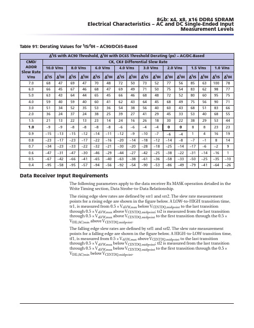
Table 91: Derating Values for t IS/t IH – AC90/DC65-BasedData Receiver Input RequirementsThe following parameters apply to the data receiver Rx MASK operation detailed in theWrite Timing section, Data Strobe-to-Data Relationship.The rising edge slew rates are defined by srr1 and srr2. The slew rate measurementpoints for a rising edge are shown in the figure below. A LOW-to-HIGH transition time,tr1, is measured from 0.5 × V diVW,max below V CENTDQ,midpoint to the last transitionthrough 0.5 × V diVW,max above V CENTDQ,midpoint ; tr2 is measured from the last transitionthrough 0.5 × V diVW,max above V CENTDQ,midpoint to the first transition through the 0.5 ×V IHL(AC)min above V CENTDQ,midpoint .The falling edge slew rates are defined by srf1 and srf2. The slew rate measurementpoints for a falling edge are shown in the figure below. A HIGH-to-LOW transition time,tf1, is measured from 0.5 × V diVW,max above V CENTDQ,midpoint to the last transitionthrough 0.5 × V diVW,max below V CENTDQ,midpoint ; tf2 is measured from the last transitionthrough 0.5 × V diVW,max below V CENTDQ,midpoint to the first transition through the 0.5 ×V IHL(AC)min below V CENTDQ,midpoint .8Gb: x4, x8, x16 DDR4 SDRAM Electrical Characteristics – AC and DC Single-Ended Input Measurement Levels2.Micron recommends calibrating pull-up ODT resistors at 0.8 × V DDQ . Other calibrationschemes may be used to achieve the linearity specification shown here.3.The tolerance limits are specified under the condition that V DDQ = V DD and V SSQ = V SS .4.The DQ-to-DQ mismatch within byte variation for a given component including DQS_tand DQS_c.5.R TT variance range ratio to R TT nominal value in a given component, including DQS_tand DQS_c.DQ-to-DQ mismatch =R TT(MAX) - R TT(MIN)R TT(NOM)× 1006.DQ-to-DQ mismatch for a x16 device is treated as two separate bytes.7.For IT, AT, and UT devices, the minimum values are derated by 9% when the device op-erates between –40°C and 0°C (TC).ODT Temperature and Voltage SensitivityIf temperature and/or voltage change after calibration, the tolerance limits widen ac-cording to the following equations and tables.˂T = T - T(@ calibration); ˂V = V DDQ - V DDQ (@ calibration); V DD = V DDQTable 129: ODT Sensitivity DefinitionsTable 130: ODT Voltage and Temperature SensitivityODT Timing DefinitionsThe reference load for ODT timings is different than the reference load used for timingmeasurements.Figure 241: ODT Timing Reference Load8Gb: x4, x8, x16 DDR4 SDRAM Electrical Characteristics – On-Die Termination Characteristics。
MEMORY存储芯片MT41K128M16JT-107 IT K中文规格书
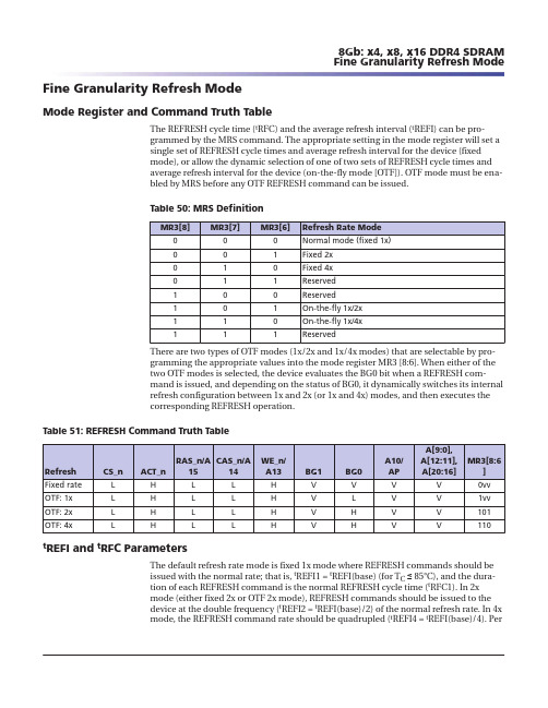
Fine Granularity Refresh ModeMode Register and Command Truth TableThe REFRESH cycle time (t RFC) and the average refresh interval (t REFI) can be pro-grammed by the MRS command. The appropriate setting in the mode register will set asingle set of REFRESH cycle times and average refresh interval for the device (fixedmode), or allow the dynamic selection of one of two sets of REFRESH cycle times andaverage refresh interval for the device (on-the-fly mode [OTF]). OTF mode must be ena-bled by MRS before any OTF REFRESH command can be issued.Table 50: MRS DefinitionThere are two types of OTF modes (1x/2x and 1x/4x modes) that are selectable by pro-gramming the appropriate values into the mode register MR3 [8:6]. When either of thetwo OTF modes is selected, the device evaluates the BG0 bit when a REFRESH com-mand is issued, and depending on the status of BG0, it dynamically switches its internalrefresh configuration between 1x and 2x (or 1x and 4x) modes, and then executes thecorresponding REFRESH operation.Table 51: REFRESH Command Truth Tablet REFI and t RFC ParametersThe default refresh rate mode is fixed 1x mode where REFRESH commands should beissued with the normal rate; that is, t REFI1 = t REFI(base) (for T C ื 85°C), and the dura-tion of each REFRESH command is the normal REFRESH cycle time (t RFC1). In 2xmode (either fixed 2x or OTF 2x mode), REFRESH commands should be issued to thedevice at the double frequency (t REFI2 = t REFI(base)/2) of the normal refresh rate. In 4xmode, the REFRESH command rate should be quadrupled (t REFI4 = t REFI(base)/4). Per8Gb: x4, x8, x16 DDR4 SDRAM Fine Granularity Refresh ModeTable 63: DBI Write, DQ Frame Format (x16) (Continued)DBI During a READ OperationIf the number of 0 data bits within a given byte lane is greater than four during a READoperation, the DRAM inverts read data on its DQ outputs and drives the DBI_n pinLOW; otherwise, the DRAM does not invert the read data and drives the DBI_n pinHIGH. The read DQ frame format is shown below for x8 and x16 configurations (the x4configuration does not support the DBI function).Table 64: DBI Read, DQ Frame Format (x8)Table 65: DBI Read, DQ Frame Format (x16)8Gb: x4, x8, x16 DDR4 SDRAM Data Bus Inversion。
- 1、下载文档前请自行甄别文档内容的完整性,平台不提供额外的编辑、内容补充、找答案等附加服务。
- 2、"仅部分预览"的文档,不可在线预览部分如存在完整性等问题,可反馈申请退款(可完整预览的文档不适用该条件!)。
- 3、如文档侵犯您的权益,请联系客服反馈,我们会尽快为您处理(人工客服工作时间:9:00-18:30)。
IC41LV1664Document Title64K x 16 bit Dynamic RAM with EDO Page ModeRevision HistoryRevision No History Draft Date Remark0A Initial Draft November 15,2001The attached datasheets are provided by ICSI. Integrated Circuit Solution Inc reserve the right to change the specifications and products. ICSI will answer to your questions about device. If you have any questions, please contact the ICSI offices.IC41LV16642Integrated Circuit Solution Inc.FEATURES•Extended Data-Out (EDO) Page Mode access cycle •TTL compatible inputs and outputs; tristate I/O •Refresh Interval: 256 cycles /4 ms•Refresh Mode: RAS -Only, CAS -before-RAS (CBR),Hidden•Single power supply:5V ± 10% (IC41C1664) 3.3V ± 10% (IC41LV1664)•Byte Write and Byte Read operation via two CAS •Industrail Temperature Range -40o C to 85o C DESCRIPTIONThe ICSI IC41C1664 and IC41LV1664 is a 65,536 x 16-bit high-performance CMOS Dynamic Random Access Memories. The IC41C1664 offer an accelerated cycle access called EDO Page Mode. EDO Page Mode allows 256 random accesses within a single row with access cycle time as short as 10 ns per 16-bit word. The Byte Write control, of upper and lower byte, makes the IC41C1664 ideal for use in 16-, 32-bit wide data bus systems.These features make the IC41C1664 and IC41LV1664 ideally suited for high-bandwidth graphics, digital signal processing,high-performance computing systems, and peripheral applications.The IC41C1664 is packaged in a 40-pin 400mil SOJ and 400mil TSOP-2.64K x 16 (1-MBIT) DYNAMIC RAM WITH EDO PAGE MODEKEY TIMING PARAMETERSParameter-25-30-35-40Unit Max. RAS Access Time (t RAC )25303540ns Max. CAS Access Time (t CAC )891011ns Max. Column Address Access Time (t AA )12161820ns Min. EDO Page Mode Cycle Time (t PC )15202325ns Min. Read/Write Cycle Time (t RC )43556575ns40-Pin SOJPIN CONFIGURATIONS40-Pin TSOP-2PIN DESCRIPTIONSA0-A7Address Inputs I/O0-15Data Inputs/Outputs WE Write Enable OE Output Enable RAS Row Address StrobeUCAS Upper Column Address Strobe LCAS Lower Column Address Strobe Vcc Power GND Ground NCNo ConnectionIC41LV1664IC41LV1664TRUTH TABLEFunction RAS LCAS UCAS WE OE Address t R/t C I/OStandby H H H X X X High-ZRead: Word L L L H L ROW/COL D OUTRead: Lower Byte L L H H L ROW/COL Lower Byte, D OUTUpper Byte, High-Z Read: Upper Byte L H L H L ROW/COL Lower Byte, High-ZUpper Byte, D OUT Write: Word (Early Write)L L L L X ROW/COL D INWrite: Lower Byte (Early Write)L L H L X ROW/COL Lower Byte, D INUpper Byte, High-Z Write: Upper Byte (Early Write)L H L L X ROW/COL Lower Byte, High-ZUpper Byte, D INRead-Write(1,2)L L L H→L L→H ROW/COL D OUT, D INEDO Page-Mode Read(2)1st Cycle:L H→L H→L H L ROW/COL D OUT2nd Cycle:L H→L H→L H L NA/COL D OUTAny Cycle:L L→H L→H H L NA/NA D OUTEDO Page-Mode Write(1)1st Cycle:L H→L H→L L X ROW/COL D IN2nd Cycle:L H→L H→L L X NA/COL D INEDO Page-Mode1st Cycle:L H→L H→L H→L L→H ROW/COL D OUT, D INRead-Write(1,2)2nd Cycle:L H→L H→L H→L L→H NA/COL D OUT, D INHidden Refresh(2)Read L→H→L L L H L ROW/COL D OUTWrite L→H→L L L L X ROW/COL D OUTRAS-Only Refresh L H H X X ROW/NA High-ZCBR Refresh(3)H→L L L X X X High-ZNotes:1.These WRITE cycles may also be BYTE WRITE cycles (either LCAS or UCAS active).2.These READ cycles may also be BYTE READ cycles (either LCAS or UCAS active).3.At least one of the two CAS signals must be active (LCAS or UCAS).4Integrated Circuit Solution Inc.IC41LV1664Functional DescriptionThe IC41C1664 and IC41LV1664 is a CMOS DRAM optimized for high-speed bandwidth, low power applica-tions. During READ or WRITE cycles, each bit is uniquely addressed through the 16 address bits. These are entered 8 bits (A0-A7) at a time. The row address is latched by the Row Address Strobe (RAS). The column address is latched by the Column Address Strobe (CAS) .The IC41C1664 and IC41LV1664 has two CAS controls, LCAS and UCAS. The LCAS and UCAS inputs internally generates a CAS signal functioning in an identical man-ner to the single CAS input on the other 64K x 16 DRAMs. The key difference is that each CAS controls its corre-sponding I/O tristate logic (in conjunction with OE and WE and RAS). LCAS controls I/O0 through I/O7 and UCAS controls I/O8 through I/O15.The IC41C1664 and IC41LV1664 CAS function is deter-mined by the first CAS (LCAS or UCAS) transitioning LOW and the last transitioning back HIGH. The two CAS controls give the IC41C1664 both BYTE READ and BYTE WRITE cycle capabilities.Memory CycleA memory cycle is initiated by bring RAS LOW and it is terminated by returning both RAS and CAS HIGH. To ensures proper device operation and data integrity any memory cycle, once initiated, must not be ended or aborted before the minimum t RAS time has expired. A new cycle must not be initiated until the minimum precharge time t RP, t CP has elapsed.Read CycleA read cycle is initiated by the falling edge of CAS or OE, whichever occurs last, while holding WE HIGH. The column address must be held for a minimum time specified by t AR. Data Out becomes valid only when t RAC, t AA, t CAC and t OE are all satisfied. As a result, the access time is dependent on the timing relationships between these parameters.Write CycleA write cycle is initiated by the falling edge of CAS and WE, whichever occurs last. The input data must be valid at or before the falling edge of CAS or WE, whichever occurs first.Refresh CycleTo retain data, 256 refresh cycles are required in each 4 ms period. There are two ways to refresh the memory.1.By clocking each of the 256 row addresses (A0 throughA7) with RAS at least once every 4 ms. Any read, write, read-modify-write or RAS-only cycle refreshes the ad-dressed row.ing a CAS-before-RAS refresh cycle. CAS-before-RAS refresh is activated by the falling edge of RAS, while holding CAS LOW. In CAS-before-RAS refresh cycle, an internal 8-bit counter provides the row ad-dresses and the external address inputs are ignored. CAS-before-RAS is a refresh-only mode and no data access or device selection is allowed. Thus, the output remains in the High-Z state during the cycle.Extended Data Out Page ModeEDO page mode operation permits all 256 columns within a selected row to be randomly accessed at a high data rate. In EDO page mode read cycle, the data-out is held to the next CAS cycle’s falling edge, instead of the rising edge. For this reason, the valid data output time in EDO page mode is extended compared with the fast page mode. In the fast page mode, the valid data output time becomes shorter as the CAS cycle time becomes shorter. Therefore, in EDO page mode, the timing margin in read cycle is larger than that of the fast page mode even if the CAS cycle time becomes shorter.In EDO page mode, due to the extended data function, the CAS cycle time can be shorter than in the fast page mode if the timing margin is the same.The EDO page mode allows both read and write opera-tions during one RAS cycle, but the performance is equivalent to that of the fast page mode in that case.Power-OnAfter application of the V CC supply, an initial pause of 200 µs is required followed by a minimum of eight initial-ization cycles (any combination of cycles containing a RAS signal).During power-on, it is recommended that RAS track with V CC or be held at a valid V IH to avoid current surges.IC41LV1664ABSOLUTE MAXIMUM RATINGS(1)Symbol Parameters Rating UnitV T Voltage on Any Pin Relative to GND5V–1.0 to +7.0V3.3V–0.5 to +4.6V CC Supply Voltage5V–1.0 to +7.0V3.3V–0.5 to +4.6I OUT Output Current50mAP D Power Dissipation1WT A Commercial Operation Temperature0 to +70°CIndustrial Operationg Temperature–40 to +85°CT STG Storage Temperature–55 to +125°CNote:1.Stress greater than those listed under ABSOLUTE MAXIMUM RATINGS may cause permanentdamage to the device. This is a stress rating only and functional operation of the device at theseor any other conditions above those indicated in the operational sections of this specification isnot implied. Exposure to absolute maximum rating conditions for extended periods may affectreliability.RECOMMENDED OPERATING CONDITIONS (Voltages are referenced to GND.) Symbol Parameter Min.Typ.Max.UnitV CC Supply Voltage5V 4.5 5.0 5.5V3.3V 3.0 3.3 3.6V IH Input High Voltage5V 2.4—V CC + 1.0V3.3V 2.0—V CC + 0.3V IL Input Low Voltage5V–1.0—0.8V3.3V–0.3—0.8T A Commercial Ambient Temperature0—70°CIndustrial Ambient Temperature–40—85°CCAPACITANCE(1,2)Symbol Parameter Max.UnitC IN1Input Capacitance: A0-A85pFC IN2Input Capacitance: RAS, UCAS, LCAS, WE, OE7pFC IO Data Input/Output Capacitance: I/O0-I/O157pFNotes:1. Tested initially and after any design or process changes that may affect these parameters.2. Test conditions: T A = 25°C, f = 1 MHz.6Integrated Circuit Solution Inc.IC41LV1664ELECTRICAL CHARACTERISTICS(1)(Recommended Operating Conditions unless otherwise noted.)Symbol Parameter Test Condition Speed Min.Max.UnitI IL Input Leakage Current Any input 0V < V IN < Vcc–1010µAOther inputs not under test = 0VI IO Output Leakage Current Output is disabled (Hi-Z)–1010µA0V < V OUT < VccV OH Output High Voltage Level I OH = –5 mA 2.4—V V OL Output Low Voltage Level I OL = +4.2 mA—0.4VI CC1Standby Current: TTL RAS, LCAS, UCAS > V IH Commerical5V—2mACommerical 3.3V—1I CC2Standby Current: CMOS RAS, LCAS, UCAS > V CC – 0.2V5V—1mA3.3V—0.5I CC3Operating Current:RAS, LCAS, UCAS,-25—170mARandom Read/Write(2,3,4)Address Cycling, t RC = t RC (min.)30—150Average Power Supply Current35—13040—120I CC4Operating Current:RAS = V IL, LCAS, UCAS,-25—170mAEDO Page Mode(2,3,4)Cycling t PC = t PC (min.)30—150Average Power Supply Current35—13040—120I CC5Refresh Current:RAS Cycling, LCAS, UCAS > V IH-25—170mARAS-Only(2,3)t RC = t RC (min.)30—150Average Power Supply Current35—13040—120I CC6Refresh Current:RAS, LCAS, UCAS Cycling-25—170mACBR(2,3,5)t RC = t RC (min.)30—150Average Power Supply Current35—13040—120Notes:1. An initial pause of 200 µs is required after power-up followed by eight RAS refresh cycles (RAS-Only or CBR) before proper deviceoperation is assured. The eight RAS cycles wake-up should be repeated any time the t REF refresh requirement is exceeded.2. Dependent on cycle rates.3. Specified values are obtained with minimum cycle time and the output open.4. Column-address is changed once each EDO page cycle.5. Enables on-chip refresh and address counters.IC41LV1664AC CHARACTERISTICS(1,2,3,4,5,6)(Recommended Operating Conditions unless otherwise noted.)-25303540Symbol Parameter Min.Max.Min.Max.Min.Max.Min.Max.Units t RC Random READ or WRITE Cycle Time43—55—65—75—nst RAC Access Time from RAS(6, 7)—25—30—35—40nst C A C Access Time from CAS(6, 8, 15)—8—9—10—11nst AA Access Time from Column-Address(6)—12—16—18—20nst RAS RAS Pulse Width2510K3010K3510K4010K nst RP RAS Precharge Time15—20—23—25—nst CAS CAS Pulse Width(26)410K910K1010K1110K nst CP CAS Precharge Time(9, 25)4—5—6—7—nst CSH CAS Hold Time (21)25—30—35—40—nst RCD RAS to CAS Delay Time(10, 20)1017102110251029nst ASR Row-Address Setup Time0—0—0—0—nst RAH Row-Address Hold Time5—5—5—5—nst ASC Column-Address Setup Time(20)0—0—0—0—nst CAH Column-Address Hold Time(20)5—5—5—5—nst AR Column-Address Hold Time22—26—30—34—ns (referenced to RAS)t RAD RAS to Column-Address Delay Time(11)813814817820nst RAL Column-Address to RAS Lead Time12—16—18—20—nst RPC RAS to CAS Precharge Time10—10—10—10—nst RSH RAS Hold Time(27)8—9—10—11—nst CLZ CAS to Output in Low-Z(15, 29)3—3—3—3—nst CRP CAS to RAS Precharge Time(21)5—5—5—5—nst OD Output Disable Time(19, 28, 29)—6—8—8—8nst OE Output Enable Time(15, 16)—8—9—10—11nst OEHC OE HIGH Hold Time from CAS HIGH10—10—10—10—nst OEP OE HIGH Pulse Width10—10—10—10—nst OES OE LOW to CAS HIGH Setup Time5—5—5—5—nst RCS Read Command Setup Time(17, 20)0—0—0—0—nst RRH Read Command Hold Time0—0—0—0—ns (referenced to RAS)(12)t RCH Read Command Hold Time0—0—0—0—ns (referenced to CAS)(12, 17, 21)t WCH Write Command Hold Time(17, 27)5—5—5—5—nst WCR Write Command Hold Time22—26—30—34—ns (referenced to RAS)(17)t WP Write Command Pulse Width(17)5—5—5—5—nst WPZ WE Pulse Widths to Disable Outputs10—10—10—10—nst RWL Write Command to RAS Lead Time(17)7—8—9—10—nst CWL Write Command to CAS Lead Time(17, 21)5—6—7—8—nst WCS Write Command Setup Time(14, 17, 20)0—0—0—0—nst DHR Data-in Hold Time (referenced to RAS)22—26—30—34—ns8Integrated Circuit Solution Inc.IC41LV1664AC CHARACTERISTICS (Continued)(1,2,3,4,5,6)(Recommended Operating Conditions unless otherwise noted.)-25303540Symbol Parameter Min.Max.Min.Max.Min.Max.Min.Max.Units t ACH Column-Address Setup Time to CAS15—15—15—15—ns Precharge during WRITE Cyclet OEH OE Hold Time from WE during4—4—4—4—ns READ-MODIFY-WRITE cycle(18)t DS Data-In Setup Time(15, 22)0—0—0—0—ns t DH Data-In Hold Time(15, 22)5—5—5—5—ns t RWC READ-MODIFY-WRITE Cycle Time65—85—95—105—ns t RWD RAS to WE Delay Time during34—46—51—56—ns READ-MODIFY-WRITE Cycle(14)t CWD CAS to WE Delay Time(14, 20)17—25—26—27—ns t AWD Column-Address to WE Delay Time(14)21—32—34—36—ns t PC EDO Page Mode READ or WRITE15—20—23—25—ns Cycle Time(24)t RASP RAS Pulse Width in EDO Page Mode2510K3010K3510K4010K ns t CPA Access Time from CAS Precharge(15)—14—18—20—22ns t PRWC EDO Page Mode READ-WRITE37—42—49—52—ns Cycle Time(24)t COH Data Output Hold after CAS LOW5—5—5—5—ns t OFF Output Buffer Turn-Off Delay from315315315315ns CAS or RAS(13,15,19, 29)t WHZ Output Disable Delay from WE315315315315ns t CLCH Last CAS going LOW to First CAS4—9—10—11—ns returning HIGH(23)t CSR CAS Setup Time (CBR REFRESH)(30, 20)5—10—10—10—ns t CHR CAS Hold Time (CBR REFRESH)(30, 21)7—10—10—10—ns t ORD OE Setup Time prior to RAS during0—0—0—0—ns HIDDEN REFRESH Cyclet REF Refresh Period (256 Cycles)—4—444ms t T Transition Time (Rise or Fall)(2, 3)150150150150nsAC TEST CONDITIONSOutput load:Two TTL Loads and 50 pF (Vcc = 5.0V ±10%)One TTL Load and 50 pF (Vcc = 3.3V ±10%)Input timing reference levels: V IH = 2.4V, V IL = 0.8V (Vcc = 5.0V ±10%);V IH = 2.0V, V IL = 0.8V (Vcc = 3.3V ±10%)Output timing reference levels: V OH = 2.0V, V OL = 0.8V (Vcc = 5V ±10%, 3.3V ±10%)IC41LV1664Notes:1.An initial pause of 200 µs is required after power-up followed by eight RAS refresh cycle (RAS-Only or CBR) before proper deviceoperation is assured. The eight RAS cycles wake-up should be repeated any time the t REF refresh requirement is exceeded. 2.V IH (MIN) and V IL (MAX) are reference levels for measuring timing of input signals. Transition times, are measured between V IHand V IL (or between V IL and V IH) and assume to be 1 ns for all inputs.3.In addition to meeting the transition rate specification, all input signals must transit between V IH and V IL (or between V IL and V IH)in a monotonic manner.4.If CAS and RAS = V IH, data output is High-Z.5.If CAS = V IL, data output may contain data from the last valid READ cycle.6.Measured with a load equivalent to one TTL gate and 50 pF.7.Assumes that t RCD≤ t RCD (MAX). If t RCD is greater than the maximum recommended value shown in this table, t RAC will increaseby the amount that t RCD exceeds the value shown.8.Assumes that t RCD≥ t RCD (MAX).9.If CAS is LOW at the falling edge of RAS, data out will be maintained from the previous cycle. To initiate a new cycle and clear thedata output buffer, CAS and RAS must be pulsed for t CP.10.Operation with the t RCD (MAX) limit ensures that t RAC (MAX) can be met. t RCD (MAX) is specified as a reference point only; if t RCDis greater than the specified t RCD (MAX) limit, access time is controlled exclusively by t CAC.11.Operation within the t RAD (MAX) limit ensures that t RCD (MAX) can be met. t RAD (MAX) is specified as a reference point only; if t RADis greater than the specified t RAD (MAX) limit, access time is controlled exclusively by t AA.12.Either t RCH or t RRH must be satisfied for a READ cycle.13.t OFF (MAX) defines the time at which the output achieves the open circuit condition; it is not a reference to V OH or V OL.14.t WCS, t RWD, t AWD and t CWD are restrictive operating parameters in LATE WRITE and READ-MODIFY-WRITE cycle only. If t WCS≥ t WCS(MIN), the cycle is an EARLY WRITE cycle and the data output will remain open circuit throughout the entire cycle. If t RWD≥ t RWD (MIN), t AWD≥ t AWD (MIN) and t CWD≥ t CWD (MIN), the cycle is a READ-WRITE cycle and the data output will contain data read from the selected cell. If neither of the above conditions is met, the state of I/O (at access time and until CAS and RAS or OE go back to V IH) is indeterminate. OE held HIGH and WE taken LOW after CAS goes LOW result in a LATE WRITE (OE-controlled) cycle.15.Output parameter (I/O) is referenced to corresponding CAS input, I/O0-I/O7 by LCAS and I/O8-I/O15 by UCAS.16.During a READ cycle, if OE is LOW then taken HIGH before CAS goes HIGH, I/O goes open. If OE is tied permanently LOW, a LATEWRITE or READ-MODIFY-WRITE is not possible.17.Write command is defined as WE going low.TE WRITE and READ-MODIFY-WRITE cycles must have both t OD and t OEH met (OE HIGH during WRITE cycle) in order to ensurethat the output buffers will be open during the WRITE cycle. The I/Os will provide the previously written data if CAS remains LOW and OE is taken back to LOW after t OEH is met.19.The I/Os are in open during READ cycles once t OD or t OFF occur.20.The first χCAS edge to transition LOW.21.The last χCAS edge to transition HIGH.22.These parameters are referenced to CAS leading edge in EARLY WRITE cycles and WE leading edge in LATE WRITE or READ-MODIFY-WRITE cycles.st falling χCAS edge to first rising χCAS edge.st rising χCAS edge to next cycle’s last rising χCAS edge.st rising χCAS edge to first falling χCAS edge.26.Each χCAS must meet minimum pulse width.st χCAS to go LOW.28.I/Os controlled, regardless UCAS and LCAS.29.The 3 ns minimum is a parameter guaranteed by design.30.Enables on-chip refresh and address counters.10Integrated Circuit Solution Inc.IC41LV1664READ CYCLENote:1.t OFF is referenced from rising edge of RAS or CAS, whichever occurs last.IC41LV1664EARLY WRITE CYCLE (OE = DON'T CARE)12Integrated Circuit Solution Inc.IC41LV1664READ WRITE CYCLE (LATE WRITE and READ-MODIFY-WRITE Cycles)IC41LV1664EDO-PAGE-MODE READ CYCLENote:1.t PC can be measured from falling edge of CAS to falling edge of CAS, or from rising edge of CAS to rising edge of CAS. Bothmeasurements must meet the t PC specifications.14Integrated Circuit Solution Inc.IC41LV1664EDO-PAGE-MODE EARLY-WRITE CYCLEIC41LV166416Integrated Circuit Solution Inc.EDO-PAGE-MODE READ-WRITE CYCLE (LATE WRITE and READ-MODIFY WRITE Cycles)Note:1.t PC is for LATE write cycles only. t PC can be measured from falling edge of CAS to falling edge of CAS , or from rising edge of CAS to rising edge of CAS . Both measurements must meet the t PC specifications.IC41LV1664EDO-PAGE-MODE READ-EARLY-WRITE CYCLE (Psuedo READ-MODIFY WRITE)IC41LV1664AC WAVEFORMSREAD CYCLE (With WE-Controlled Disable)RAS-ONLY REFRESH CYCLE (OE, WE = DON'T CARE)18Integrated Circuit Solution Inc.IC41LV1664CBR REFRESH CYCLE (Addresses; WE, OE = DON'T CARE)HIDDEN REFRESH CYCLE(1)(WE = HIGH; OE = LOW)Notes:1.A Hidden Refresh may also be performed after a Write Cycle. In this case, WE = LOW and OE = HIGH.2.t OFF is referenced from rising edge of RAS or CAS, whichever occurs last.IC41LV166420Integrated Circuit Solution Inc.ORDERING INFORMATION IC41C1664Commercial Range: 0°C to 70°CSpeed (ns)Order Part No.Package 25IC41C1664-25K 400mil SOJ IC41C1664-25T 400mil TSOP-230IC41C1664-30K 400mil SOJ IS41C1664-30T 400mil TSOP-235IC41C1664-35K 400mil SOJ IC41C1664-35T 400mil TSOP-240IC41C1664-40K 400mil SOJ IC41C1664-40T400mil TSOP-2ORDERING INFORMATION:IC41LV1664Commercial Range: 0°C to 70°CSpeed (ns)Order Part No.Package 30IC41LV1664-30K 400mil SOJ IC41LV1664-30T 400mil TSOP-235IC41LV1664-35K 400mil SOJ IC41LV1664-35T 400mil TSOP-240IC41LV1664-40K 400mil SOJ IC41LV1664-40T400mil TSOP-2Industrial Range: -40°C to 85°CSpeed (ns)Order Part No.Package 25IC41C1664-25KI 400mil SOJ IC41C1664-25TI 400mil TSOP-230IC41C1664-30KI 400mil SOJ IC41C1664-30TI 400mil TSOP-235IC41C1664-35KI 400mil SOJ IC41C1664-35TI 400mil TSOP-240IC41C1664-40KI 400mil SOJ IC41C1664-40TI400mil TSOP-2Industrial Range: -40°C to 85°CSpeed (ns)Order Part No.Package 30IC41LV1664-30K 400mil SOJ IC41LV1664-30T 400mil TSOP-235IC41LV1664-35KI 400mil SOJ IC41LV1664-35TI 400mil TSOP-240IC41LV1664-40KI 400mil SOJ IC41LV1664-40TI400mil TSOP-2IC41C1664IC41LV1664Integrated Circuit Solution Inc.21DR033-0A 11/15/2001Integrated Circuit Solution Inc.HEADQUARTER:NO.2, TECHNOLOGY RD. V, SCIENCE-BASED INDUSTRIAL PARK,HSIN-CHU, TAIWAN, R.O.C.TEL: 886-3-5780333Fax: 886-3-5783000BRANCH OFFICE:7F, NO. 106, SEC. 1, HSIN-TAI 5TH ROAD,HSICHIH TAIPEI COUNTY, TAIWAN, R.O.C.TEL: 886-2-26962140FAX: 886-2-26962252元器件交易网。