IR2011SPBF;IR2011PBF;IR2011STRPBF;IR2011;IR2011S;中文规格书,Datasheet资料
ir2101strpbf使用方法
ir2101strpbf是一种电子元件,常用于驱动高压IGBT或MOSFET。
它具有双通道、高速和低反转波形失真的特点,在各种工业应用中被广泛使用。
在本文中,我们将介绍ir2101strpbf的使用方法,帮助您更好地理解和应用这一元件。
一、ir2101strpbf的基本性能参数ir2101strpbf是一种双通道驱动器,具有以下基本性能参数:1. 工作电压:10V至20V2. 最大输出电流:210mA3. 输出峰值电流:2A4. 输出峰值电压:20V5. 工作温度范围:-40℃至125℃二、ir2101strpbf的引脚功能和连接方式ir2101strpbf的引脚一共有8个,分别为HO, LO, VS, COM, VB, VCC, IN和SD。
其中,HO和LO为驱动输出端,VS和COM为高、低侧驱动器的电源端,VB为反相器的电源端,VCC为逻辑输入端的电源端,IN为接受逻辑输入的端口,SD为关断保护引脚。
在使用ir2101strpbf时,需要按照以下连接方式进行连接:1. 将HO连接至高侧功率MOSFET或IGBT的门极,LO连接至低侧功率MOSFET或IGBT的门极。
2. VS和COM需要接入电源电压,VB接入反相器的电源电压。
3. VCC接入逻辑输入端的电源电压,IN接收逻辑输入信号。
4. SD接入一个适当的电阻用于关断保护。
三、ir2101strpbf的使用注意事项在使用ir2101strpbf时,需要注意以下事项:1. 确保连接的电源电压在规定范围内,避免过高或过低的电压对元件造成损害。
2. 确保逻辑输入信号的幅值和频率符合规格书中的要求,避免过大或过小的信号对元件造成损害或性能下降。
3. 在布局和连接时,要注意防止电磁干扰和电源噪声对驱动器的影响,保证整个系统的稳定性和可靠性。
4. 对于高压、高频率和高功率的应用,需要特别注意元件的散热和安全问题,避免过热和短路等情况的发生。
四、ir2101strpbf的应用领域ir2101strpbf可广泛应用于各种需要高速、低失真的功率开关控制电路中,例如:1. 三相逆变器2. 电机驱动器3. 换流电源4. 频率变换器5. 电力因数校正器6. 太阳能逆变器在这些应用中,ir2101strpbf可以有效地驱动功率开关器件,提高系统的运行效率和稳定性。
IR2010SPBF中文资料
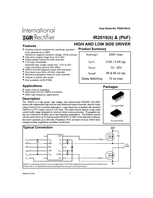
Packages
14-Lead PDIP 16-Lead SOIC
Typical Connection
200V
HO
VDD
VDD
VB
HIN
HIN
VS
SD
SD
LIN
LIN
VCC
VSS
VSS
COM
VCC
LO
(Refer to Lead Assignments for correct configuration). This/These diagram(s) show electrical connections only. Please refer to our Application Notes and DesignTips for proper circuit board layout.
元器件交易网
Data Sheet No. PD60195-D
IR2010(S) & (PbF)
Features
HIGH AND LOW SIDE DRIVER
• Floating channel designed for bootstrap operation Product Summary
Package power dissipation @ TA ≤ +25°C (14 lead DIP) (16 lead SOIC)
Thermal resistance, junction to ambient
(14 lead DIP)
(16 lead SOIC)
Junction temperature
Symbol
VB VS VHO VCC VLO VDD VSS VIN dVs/dt PD
IR2153SPBF;IR2153PBF;IR2153DPBF;IR2153STRPBF;IR2153;中文规格书,Datasheet资料

Features••15.6V zener clamp on Vcc •True micropower start up•Tighter initial deadtime control••••Lower power level-shifting circuit•••Low side output in phase with R T•••ESD protection on all leads •Also available LEAD-FREE(NOTE:For new designs, we recommendIR’s new product IRS2153D)SELF-OSCILLATING HALF-BRIDGE DRIVERProduct SummaryTypical Connections600V MAXIR2153(D)(S) &(PbF)Descriptionporates a high voltage half-bridge gate driver with a front end oscillator similar to the industry standard CMOS 555 timer. The IR2153 provides more functionality and is easier to use than previous ICs. A shutdown feature has been designed into the C T pin, so that both gate driver outputs can be disabled using a low voltage control signal. In addition, the gate driver output pulse widths are the same once the rising undervoltage lockout threshold on V CC has been reached, resulting in a more stable profile of frequency vs time at startup.Noise immunity has been improved significantly, both by lowering the peak di/dt of the gate drivers, and by increasing the undervoltage lockout hysteresis to 1V. Finally, special attention has been payed to maximizing the latch immunity of the device, and providing comprehensive ESD protection on all pins.8 Lead SOIC Data Sheet No. PD60062 revOIR2153(D)(S) & (PbF)NOTE:For new designs, we recommend IR’s new product IRS2153DNote 1:This IC contains a zener clamp structure between the chip V CC and COM which has a nominal breakdown voltage of 15.6V. Please note that this supply pin should not be driven by a DC, low impedance power source greater than the V CLAMP specified in the Electrical Characteristics section.Note 2:Care should be taken to avoid output switching conditions where the V S node flies inductively below ground by more than 5V.Note 3:Enough current should be supplied to the V CC pin of the IC to keep the internal 15.6V zener diode clamping the voltage at this pin.Recommended Operating ConditionsFor proper operation the device should be used within the recommended conditions.Absolute Maximum RatingsAbsolute maximum ratings indicate sustained limits beyond which damage to the device may occur. All voltage param-eters are absolute voltages referenced to COM, all currents are defined positive into any lead. The thermal resistance and power dissipation ratings are measured under board mounted and still air conditions.IR2153(D)(S) & (PbF)NOTE:For new designs, we recommendIR’s new product IRS2153DSymbol ComponentMin.Max.UnitsR T Timing resistor value 10— k ΩC TC T pin capacitor value330—pFRecommended Component ValuesIR2153(D)(S) & (PbF)NOTE:For new designs, we recommend IR’s new product IRS2153DElectrical CharacteristicsV BIAS (V CC , V BS ) = 12V, C L = 1000 pF, C T = 1 nF and T A = 25°C unless otherwise specified. The V IN , V TH and I IN parameters are referenced to COM. The V O and I O parameters are referenced to COM and are applicable to the respective output leads: HO or LO.IR2153(D)(S) & (PbF)NOTE:For new designs, we recommendIR’s new product IRS2153DSymbolDescriptionV CC Logic and internal gate drive supply voltage R T Oscillator timing resistor input C T Oscillator timing capacitor input COM IC power and signal ground LO Low side gate driver outputV S High voltage floating supply return HO High side gate driver outputV BHigh side gate driver floating supplyLead Definitions8 Lead PDIP 8 Lead SOICIR2153DIR2153(S)NOTE: The IR2153D is offered in 8 lead PDIP only.Electrical Characteristics (cont.)IR2153(D)(S) & (PbF)NOTE:For new designs, we recommendIR’s new product IRS2153DFunctional Block Diagram for IR2153(S) Functional Block Diagram for IR2153DIR2153(D)(S) & (PbF)NOTE:For new designs, we recommend IR’s new product IRS2153DFigure 1. Input/Output Timing DiagramFigure 3. Deadtime Waveform DefinitionsR TTCLAMPR T Figure 2. Switching Time Waveform Definitions(HO)(LO)IR2153(D)(S) & (PbF)NOTE:For new designs, we recommendIR’s new product IRS2153DLEADFREE PART MARKING INFORMATIONORDER INFORMATIONBasic Part (Non-Lead Free)8-Lead PDIP IR2153 order IR21538-Lead SOIC IR2153S order IR2153S 8-Lead PDIP IR2153D order IR2153DLeadfree Part8-Lead PDIP IR2153 order IR2153PbF 8-Lead SOIC IR2153S order IR2153SPbF 8-Lead PDIP IR2153D order IR2153DPbFIR WORLD HEADQUARTERS: 233 Kansas St., El Segundo, California 90245 Tel: (310) 252-7105This product has been qualified per industrial levelData and specifications subject to change without notice. 2/8/2006Per SCOP 200-002分销商库存信息:IRIR2153SPBF IR2153PBF IR2153DPBF IR2153STRPBF IR2153IR2153SIR2153STR IR2153D。
IR1155STRPBF;IR1155SPBF;中文规格书,Datasheet资料
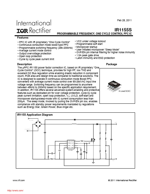
Feb 28, 2011IR1155SPROGRAMMABLE FREQUENCY, ONE CYCLE CONTROL PFC ICFeaturesDescription Package• PFC IC with IR proprietary “One Cycle Control” • Continuous conduction mode boost type PFC • Programmable switching frequency (48k-200kHz) • Average current mode control • Output overvoltage protection • Open loop protection • Cycle by cycle peak current limit • VCC under voltage lockout• Programmable soft start • Micropower startup • User initiated micropower “Sleep Mode”• OVP/EN pin internal filtering for higher noise immunity • 1.5A peak gate drive• Latch immunity and ESD protection The μPFC IR1155 power factor correction IC, based on IR proprietary "OneCycle Control" (OCC) technique, provides for high PF, low THD and excellent DC Bus regulation while enabling drastic reduction in component count, PCB area and design time as compared to traditional solutions. The IC is designed to operate in continuous conduction mode Boost PFC converters with average current mode control over 85-264VAC input line voltage range. Switching frequency can be programmed to anywhere between 48kHz to 200kHz based on the specific application requirement. In addition, IR1155 offers several advanced system-enabling and protective features such as dedicated pin for over voltage protection, cycle by cycle peak current limitation, open loop protection, V CCUVLO, soft-start and micropower startup/sleep-mode with IC current consumption less than 200µA. The sleep mode, invoked by pulling the OVP/EN pin low, enables compliance with standby power requirements mandated by regulations such as Energy Star, Green Power, Blue Angel etc.Qualification InformationIndustrialQualification Level Comments: This family of ICs has passed JEDEC’s Industrialqualification. IR’s Consumer qualification level is granted byextension of the higher Industrial level.Moisture Sensitivity LevelMSL2 260°C(per IPC/JEDEC J-STD-020)Machine ModelClass A(per JEDEC standard JESD22-A115)ESDHuman Body ModelClass 1B (passes 500V)(per EIA/JEDEC standard EIA/JESD22-A114)IC Latch-Up Test Class I, Level A (per JESD78)RoHS Compliant YesAbsolute Maximum RatingsParameter Symbol Min. Max. Units RemarksVCC Voltage V CC -0.3 20 VFREQ Voltage V FREQ -0.3 6.5 VISNS Voltage V ISNS -10 0.3 VVFB, OVP Voltage V FB, V OVP -0.3 6.5 VCOMP Voltage V COMP -0.3 6.5 VGATE Voltage V GATE -0.3 18 VISNS Current I ISNS -2 2 mAJunction Temperature T J -40 150 °CStorage Temperature T S -55 150 °CThermal ResistanceJunction to AmbientRθJA128 °C/WPackage Power Dissipation P D976 mWT AMB = 25°CRecommended Operating ConditionsRecommended operating conditions for reliable operation with marginParameter SymbolMin.Typ.Max.UnitsRemarks Supply Voltage V CC12 19 VJunction Temperature T J -25 125 °CSwitching Frequency F SW 48 200 kHzElectrical CharacteristicsThe electrical characteristics involve the spread of values guaranteed within the specified supply voltage and junction temperature range T J from –25 °C to 125°C. Typical values represent the median values, which are related to 25°C. If not otherwise stated, a supply voltage of V CC =15V is assumed for test condition . Supply SectionParameter Symbol Min. Typ. Max. Units Remarks VCC Turn On ThresholdV CC ON 10.65 11.3 11.95 V VCC Turn OffThreshold (Under Voltage Lock Out) V CC UVLO 9.2 9.8 10.4 V VCC Turn On/Off Hysteresis V CC HYST 1.5VOperating CurrentI CC 10 13 mA C load =1nF, F SW =181kHz6 8 mAStandby Mode (Inactive Gate, Inactive Internal Oscillator)V FB <V OLPSee State Transition Diagram Startup CurrentI CCSTART175 uA V CC =V CC ON - 0.1VSleep CurrentI SLEEP 125 200 uASleep Mode (Inactive Gate,Inactive Oscillator)- V OVP <V SLEEP,OFFSee State Transition Diagram Sleep ModeThreshold (Enable)V SLEEP,ON0.80 0.90 1.00 VIC Enable threshold,Bias on OVP pinSleep ModeThreshold (Disable)V SLEEP,OFF 0.53 0.60 0.67VIC Disable threshold, Bias on OVP pinOscillator SectionParameter SymbolMin.Typ.Max.UnitsRemarks Switching Frequency F SW 48 200kHz200khz:C=430pFapprox.48kHz: C=2nF approx. Oscillator Charge Current I OSC(CHG)200 µAOscillator DischargeCurrentI OSC(DCHG) 6.6 mAOscillator Peak V OSC PK 4 VOscillator Valley V OSC VAL 2 V5 %C=2nF,T A = 25°CInitial Accuracy F SW ACC8 %C=500pF,T A = 25°C Voltage Stability V STAB 0.2 1 % 14V < V CC < 19V Temperature Stability T STAB 2 %-25°C≤ T J≤ 125°CTotal Variation F VT 10 %Line&Temperature Maximum Duty Cycle D MAX94 99 %Minimum Duty Cycle D MIN0 %PulseSkippingProtection SectionParameter SymbolMin.Typ.Max.UnitsRemarksOpen Loop Protection (OLP) V FB Threshold V OLP 17 19 21 %V REF Bias on VFB pinOutput Over Voltage Protection (OVP) V OVP 104.5 106.5 108.5 %V REF Bias on OVP/EN pinOutput Over Voltage Protection (OVP) Reset V OVP(RST) 100.2 102.2 104.2 %V REF Bias on OVP/EN pinPeak Current LimitProtection (IPK LMT) I SNSVoltage ThresholdV ISNS-0.85 -0.77 -0.69 V Bias on ISNS pin OVP Input Bias Current I OVP(Bias)-0.2 µAInternal Voltage Reference SectionVoltage Error Amplifier SectionParameter Symbol Min. Typ. Max. Units Remarks Transconductance g m 35 50 65 µS 30 44 58 T AMB = 25°C Source CurrentI OVEA(SRC)20 44 90µA -25°C ≤T AMB ≤ 125°C -57 -43 -30 T AMB = 25°C Sink Current I OVEA(SNK)-90 -43 -20µA -25°C ≤T AMB ≤ 125°CSoft Start Delay Time t SS35 msec R GAIN = 1k Ω, C ZERO = 0.33uF,C POLE = 0.01uF V COMP Voltage (Fault) V COMP FLT 1 1.4 V@ 100µA steady statecurrentEffective V COMP Voltage V COMP EFF 4.6 4.9 5.2 V VFB Input Bias Current I IB(Bias)-0.2 µA V FB =4.9VOutput Low Voltage V OL 0.25 V Output High Voltage V OH 5 5.4 V V COMP Start Voltage V COMP START240 340 460 mVParameter Symbol Min. Typ. Max. Units Remarks Reference Voltage V REF 4.9 5 5.1 V T A = 25°C Line Regulation R REG1020mV14 V < V CC < 19V Temp Stability T STAB 0.4 % -25°C ≤ T AMB ≤ 125°C Total VariationΔV TOT4.855.1VLine & TemperatureCurrent Amplifier SectionUnitsRemarksMax.Parameter SymbolMin.Typ.DC Gain g DC 3.1 V/VCorner Frequency f C 5 kHz - Average current mode, Note 1Note1Input Offset Voltage V IO 4 16 mVI SNS Bias Current I ISNS(Bias) -57 -13 µABlanking Time T BLANK220 370 520 nsGate Driver SectionUnitsMax.Remarks Parameter SymbolMin.Typ.Gate Low Voltage V GLO 0.8 VI GATE=200mAclamp12 13 14 VGateInternalGate High Voltage V GTHV CC = 11.5V10 VRise Time t r20 nsC LOAD = 1nFFall Time t f20 nsC LOAD = 1nFC LOAD = 10nF, Note 1Output Peak Current I OPK 1.5 AGate Voltage @ Fault V G fault 0.08I GATE = 20mAVNote 1 – Guaranteed by design, but Not tested in productionLead Assignments & DefinitionsBlock DiagramVFBCOMPOVPNote: Soft-Start & Normal modes are essentially the same (differentiation above is for purpose of clarity only)VCC Undervoltage LockoutV o l t a g e o n V C C p i nTiming DiagramsOutput Protection分销商库存信息:IRIR1155STRPBF IR1155SPBF。
IRS2101STRPBF中文资料
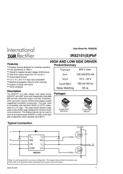
2
元器件交易网
IRS2101(S)PbF
Dynamic Electrical Characteristics
VBIAS (VCC, VBS) = 15 V, CL = 1000 pF and TA = 25 °C unless otherwise specified.
50 1.0 0.625 125 200 150 150 300
Units
V
V/ns W
°C/W °C
Recommended Operating Conditions
The input/output logic timing diagram is shown in Fig. 1. For proper operation the device should be used within the recommended conditions. The VS offset rating is tested with all supplies biased at a 15 V differential.
Package power dissipation @ TA ≤ +25 °C
Thermal resistance, junction to ambient
Junction temperature Storage temperature Lead temperature (soldering, 10 seconds)
V
— 0.05 0.2
IO = 2 mA
— 0.02 0.1
—
—
50
VB = VS = 600 V
—
30 55
— 150 270 µA
VIN = 0 V or 5 V
IR2136STRPBF 参数设置
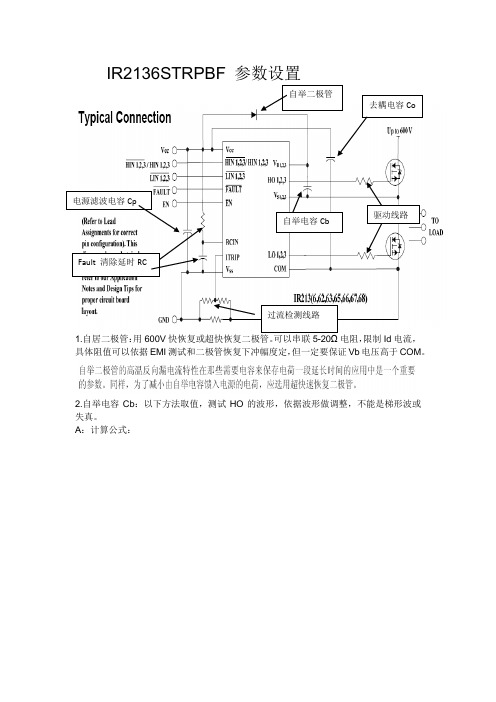
IR2136STRPBF1.自居二极管:用600V 快恢复或超快恢复二极管。
可以串联5-20Ω电阻,限制Id 电流,具体阻值可以依据EMI 测试和二极管恢复下冲幅度定,但一定要保证Vb 电压高于COM 。
2.自举电容Cb :以下方法取值,测试HO 的波形,依据波形做调整,不能是梯形波或失真。
A :计算公式:自举电容Cb驱动线路B:使用经验值3.去耦电路:Co: Low ESR,该电容支持低端输出供电和自举重充电,电容值是Cb的10倍。
太小会造成VCC供电不足,影响2136驱动能力,严重的会引起误保护。
4.过流检测线路:过流检测线路的设计,典型线路是用较大的电流检测电阻,将检测到的电压进行分压后再送到2136 Itrip脚进行比较滤波处理。
依据下面IR2136内部结构图,过流检测线路可以简化为RC检测滤波。
过流检测电阻可以依据R=0.46/Iocp 计算,Iopc为过流保护电流。
RC滤波中的RC取值:R=410-1Kohm,C=56-470pF,具体可测试Itrip电流波形和实际的Iocp 做调整,电容太大会造成保护的延迟,造成炸机,太小会误保护。
5. 电源滤波电容Cp :测试IR2136 Vcc 电压的纹波,如果是低频纹波使用与Co 相同的电容;如果是高频噪音加独石电容或金属盒装电容,104-105pF.6. Fault 清除延时RCC :建议最小用103pF, R 的取值依据延迟时间T 与C 定,R=T/C.先按R=2M Ω,C=1nF, T=1.3/1.65/2mS.再测试/Fault 和RCIN 波形,进行调整。
7. 驱动线路:MOS/IBGT 驱动线路: 驱动线路中的电阻先选10-20ohm 电阻,再根据所选MOS/IGBT G 极波形和EMI 测试情况确定。
建议加加速关断电路,减小IGBT 的关断时的拖尾时间。
并联二极管使用开关管1N4148,并串联适当的电阻限制电流.刘 航 20120824 SZ 。
IR2103SPBF;IR2103PBF;IR2103STRPBF;IR2103;IR2103S;中文规格书,Datasheet资料
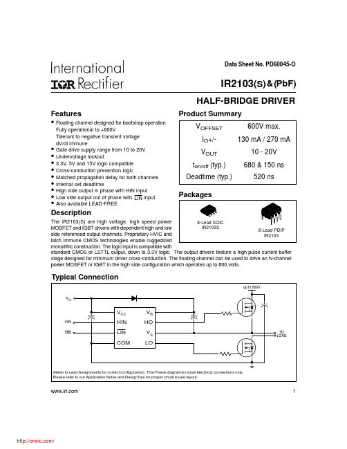
Data Sheet No. PD60045-OTypical ConnectionProduct SummaryHALF-BRIDGE DRIVERFeatures•Fully operational to +600VdV/dt immune••Undervoltage lockout••Cross-conduction prevention logic••Internal set deadtime•••Also available LEAD-FREEDescriptionpower MOSFET or IGBT in the high side configuration which operates up to 600 volts. 1IR2103(S ) & (PbF)IR2103(S) & (PbF)Absolute Maximum RatingsAbsolute maximum ratings indicate sustained limits beyond which damage to the device may occur. All voltage param-eters are absolute voltages referenced to COM. The thermal resistance and power dissipation ratings are measured under board mounted and still air conditions.Note 1: Logic operational for V S of -5 to +600V. Logic state held for V S of -5V to -V BS . (Please refer to the Design Tip DT97-3 for more details).IR2103(S) & (PbF) 3Static Electrical CharacteristicsV BIAS (V CC , V BS ) = 15V and T A = 25°C unless otherwise specified. The V IN , V TH and I IN parameters are referenced to COM. The V O and I O parameters are referenced to COM and are applicable to the respective output leads: HO or LO.Dynamic Electrical CharacteristicsV BIAS (V CC , V BS ) = 15V, C L = 1000 pF and T A = 25°C unless otherwise specified.IR2103(S) & (PbF)4Functional Block DiagramLead DefinitionsSymbol DescriptionHIN Logic input for high side gate driver output (HO), in phase Logic input for low side gate driver output (LO), out of phase VB High side floating supply HO High side gate drive output V S High side floating supply return V CC Low side and logic fixed supply LO Low side gate drive output COMLow side returnLINLead Assignments8 Lead PDIP 8 Lead SOICIR2103IR2103S12348765V CC HIN LIN COMV B HO V S LO12348765V CC HIN LIN COMV B HO V S LOIR2103(S) & (PbF) 5Figure 1. Input/Output Timing DiagramLINHOLOHINFigure 4. Deadtime Waveform DefinitionsFigure 2. Switching Time Waveform DefinitionsLOIR2103(S) & (PbF)6IR2103(S) & (PbF) 7IR2103(S) & (PbF)8IR2103(S) & (PbF)9IR2103(S) & (PbF)10vs Temperaturevs Voltage分销商库存信息:IRIR2103SPBF IR2103PBF IR2103STRPBF IR2103IR2103S IR2103STR。
ir2117strpbf规格书
ir2117strpbf规格书【实用版】目录1.产品概述2.主要特性3.规格参数4.应用领域5.环境要求6.安全信息7.结构说明8.工作原理9.测试方法10.维护与保养正文1.产品概述ir2117strpbf 是一种高性能、低成本的电子元器件,具有出色的稳定性和可靠性。
它广泛应用于各种电子设备和系统中,为设备提供稳定的电源和信号传输功能。
2.主要特性ir2117strpbf 具有以下主要特性:- 高稳定性:在恶劣的工作环境下,仍能保持稳定的工作性能。
- 低失真:信号传输过程中失真度低,保证了信号的完整性和准确性。
- 宽工作温度范围:能在 -40℃至 +125℃的温度范围内正常工作。
- 抗干扰能力强:能有效抵抗各种电磁干扰,保证设备的正常运行。
3.规格参数ir2117strpbf 的规格参数如下:- 电压范围:3.3V-5V- 电流范围:50mA-100mA- 工作温度范围:-40℃至 +125℃- 存储温度范围:-40℃至 +125℃- 抗静电能力:±15KV- 封装形式:SOP-84.应用领域ir2117strpbf 广泛应用于以下领域:- 电子消费品:如电视机、收音机、音响设备等。
- 通讯设备:如手机、电话机、传真机等。
- 计算机及周边设备:如电脑、路由器、打印机等。
- 工业控制设备:如工控机、可编程控制器等。
5.环境要求为了保证 ir2117strpbf 的正常工作和延长使用寿命,应满足以下环境要求:- 避免阳光直射和潮湿环境。
- 避免暴露在高温、低温、高湿度的环境中。
- 避免与腐蚀性物质接触。
- 避免强烈的机械振动和冲击。
6.安全信息在操作和使用 ir2117strpbf 时,请注意以下安全信息:- 请勿用湿手触摸或操作设备。
- 请勿在未断电的情况下拆卸设备。
- 请确保设备接地良好,以防止静电损伤。
- 如有异常现象,请立即停止使用并联系专业人员处理。
7.结构说明ir2117strpbf 的结构说明如下:- 引脚 1:电源正极(VCC)- 引脚 2:电源负极(GND)- 引脚 3:输出信号(OUT)- 引脚 4:控制信号(CTRL)- 引脚 5:公共地(GND)- 引脚 6:公共地(GND)- 引脚 7:公共地(GND)- 引脚 8:输出信号(OUT)8.工作原理ir2117strpbf 的工作原理如下:当控制信号(CTRL)为高电平时,输出信号(OUT)跟随输入信号;当控制信号为低电平时,输出信号呈高阻态。
IR2153STRPBF中文资料
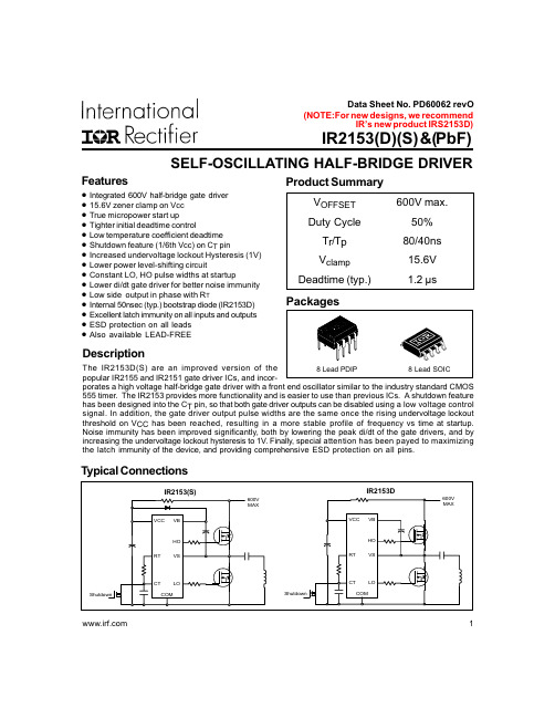
Features••15.6V zener clamp on Vcc •True micropower start up•Tighter initial deadtime control••••Lower power level-shifting circuit•••Low side output in phase with R T•••ESD protection on all leads •Also available LEAD-FREE(NOTE:For new designs, we recommendIR’s new product IRS2153D)SELF-OSCILLATING HALF-BRIDGE DRIVERProduct SummaryTypical ConnectionsIR2153(D)(S) &(PbF)Descriptionporates a high voltage half-bridge gate driver with a front end oscillator similar to the industry standard CMOS 555 timer. The IR2153 provides more functionality and is easier to use than previous ICs. A shutdown feature has been designed into the C T pin, so that both gate driver outputs can be disabled using a low voltage control signal. In addition, the gate driver output pulse widths are the same once the rising undervoltage lockout threshold on V CC has been reached, resulting in a more stable profile of frequency vs time at startup.Noise immunity has been improved significantly, both by lowering the peak di/dt of the gate drivers, and by increasing the undervoltage lockout hysteresis to 1V. Finally, special attention has been payed to maximizing the latch immunity of the device, and providing comprehensive ESD protection on all pins. 1IR2153(D)(S) & (PbF)2NOTE:For new designs, we recommend IR’s new product IRS2153DNote 1:This IC contains a zener clamp structure between the chip V CC and COM which has a nominal breakdown voltage of 15.6V. Please note that this supply pin should not be driven by a DC, low impedance power source greater than the V CLAMP specified in the Electrical Characteristics section.Note 2:Care should be taken to avoid output switching conditions where the V S node flies inductively below ground by more than 5V.Note 3:Enough current should be supplied to the V CC pin of the IC to keep the internal 15.6V zener diode clamping the voltage at this pin.Recommended Operating ConditionsFor proper operation the device should be used within the recommended conditions.Absolute Maximum RatingsAbsolute maximum ratings indicate sustained limits beyond which damage to the device may occur. All voltage param-eters are absolute voltages referenced to COM, all currents are defined positive into any lead. The thermal resistance and power dissipation ratings are measured under board mounted and still air conditions.IR2153(D)(S) & (PbF)3Symbol ComponentMin.Max.UnitsR T Timing resistor value 10— k ΩC TC T pin capacitor value330—pFRecommended Component ValuesIR2153(D)(S) & (PbF)4NOTE:For new designs, we recommend IR’s new product IRS2153DElectrical CharacteristicsV BIAS (V CC , V BS ) = 12V, C L = 1000 pF, C T = 1 nF and T A = 25°C unless otherwise specified. The V IN , V TH and I INparameters are referenced to COM. The V O and I O parameters are referenced to COM and are applicable to the respective output leads: HO or LO.IR2153(D)(S) & (PbF)5SymbolDescriptionV CC Logic and internal gate drive supply voltage R T Oscillator timing resistor input C T Oscillator timing capacitor input COM IC power and signal ground LO Low side gate driver outputV S High voltage floating supply return HO High side gate driver outputV BHigh side gate driver floating supplyLead Definitions8 Lead PDIP 8 Lead SOICIR2153DIR2153(S)NOTE: The IR2153D is offered in 8 lead PDIP only.Electrical Characteristics (cont.)IR2153(D)(S) & (PbF) 6NOTE:For new designs, we recommendIR’s new product IRS2153DFunctional Block Diagram for IR2153(S) Functional Block Diagram for IR2153DIR2153(D)(S) & (PbF)8NOTE:For new designs, we recommend IR’s new product IRS2153DFigure 1. Input/Output Timing DiagramFigure 3. Deadtime Waveform DefinitionsR TTCLAMPR T Figure 2. Switching Time Waveform Definitions(HO)(LO)IR2153(D)(S) & (PbF)9Per SCOP 200-002。
ir2112strpbf规格书
ir2112strpbf规格书IR2112STRPBF是一款电路驱动芯片,被广泛应用于直流至交流(DC-AC)转换器、电机驱动和逆变器等领域。
本文将围绕IR2112STRPBF规格书展开阐述,分步骤介绍该芯片的性能指标、引脚功能、电气特性以及应用场景。
一、性能指标IR2112STRPBF的主要性能指标包括主电源电压、引脚输入电压、输出电流、输出功率等。
其中,主电源电压为10V至20V,引脚输入电压为-0.5V至+5V,输出电流最大为2A,输出功率最大为10W。
二、引脚功能IR2112STRPBF芯片共有14个引脚,其功能如下:1. HO:高侧驱动器输出,用于驱动功率开关管;2. HO-:带负载下的高侧驱动器输出,与HO引脚互补;3. VS:高侧驱动器电源,接受10V至20V的电源电压;4. VB:串联补偿器输入,用于补偿之间延迟;5. LG:逻辑地面,用于引脚与芯片之间的接地;6. VCC:低侧驱动器电源,接受10V至20V的电源电压;7. VB-:带负载下的串联补偿器输入,与VB引脚互补;8. SD:PWM延迟,提供PWM开关时间的延迟;9. IN+: 输入控制信号+,逻辑输入为高电平时产生;10. IN-:输入控制信号-,逻辑输入为低电平时产生;11. COM:低侧驱动器输出,用于驱动功率开关管;12. COM-:带负载下的低侧驱动器输出,与COM引脚互补;13. VS-:低侧驱动器电源,接受10V至20V的电源电压;14. HO+: 高侧浮动输出+,适用于高侧无级反激拓扑。
三、电气特性IR2112STRPBF芯片的电气特性包括开路电压、输出电流、输出功率、低电平输入电压、高电平输入电压等指标。
其中,开路电压为600V,输出电流为2A,输出功率为10W,低电平输入电压为0.8V,高电平输入电压为2.4V。
四、应用场景IR2112STRPBF芯片在电力电子设备中被广泛应用,主要应用于驱动功率开关管的直流交流转换器、逆变器和电机驱动等领域。
IR1153STRPBF;IR1153SPBF;中文规格书,Datasheet资料
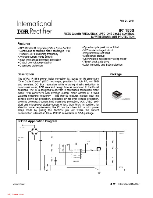
Feb 21, 2011IR1153SFIXED 22.2kHz FREQUENCY, µPFC ONE CYCLE CONTROLIC WITH BROWN-OUT PROTECTIONFeaturesDescription Package• PFC IC with IR proprietary “One Cycle Control” • Continuous conduction mode boost type PFC • Fixed 22.2kHz switching frequency • Average current mode control • Input line sensed brownout protection • Output overvoltage protection • Open loop protection • Cycle by cycle peak current limit• VCC under voltage lockout • Programmable soft start • Micropower startup • User initiated micropower “Sleep Mode” • 750mA peak gate drive• Latch immunity and ESD protection The μPFC IR1153 power factor correction IC, based on IR proprietary"One Cycle Control" (OCC) technique, provides for high PF, low THD and excellent DC Bus regulation while enabling drastic reduction incomponent count, PCB area and design time as compared to traditional solutions. The IC is designed to operate in continuous conduction mode Boost PFC converters with average current mode control at a fixed 22.2kHz switching frequency. The IR1153 features include input-line sensed brown-out protection, dedicated pin for over voltage protection, cycle by cycle peak current limit, open loop protection, VCC UVLO, soft-start and micropower startup current of less than 75µA. In addition, for standby power requirements, the IC can be driven into a micropower sleep mode by pulling the OVP/EN pin low where the current consumption is less than 75uA. IR1153 is available in SO-8 package.Qualification InformationIndustrialQualification Level Comments: This family of ICs has passed JEDEC’s Industrial qualification.IR’s Consumer qualification level is granted by extension of the higherIndustrial level.Moisture Sensitivity LevelMSL2 260°C(per IPC/JEDEC J-STD-020)Machine ModelClass A(per JEDEC standard JESD22-A115)ESDHuman Body ModelClass 1A(per EIA/JEDEC standard EIA/JESD22-A114)IC Latch-Up Test Class I, Level A (per JESD78)RoHS Compliant YesAbsolute Maximum RatingsStresses beyond those listed under “Absolute Maximum Ratings” may cause permanent damage to the device. These are stress ratings only and functional operation of the device at these conditions is not implied. All voltages are absolute voltages referenced to COM. Thermal resistance and power dissipation are measured under board mounted and still air conditions.Parameters Symbol Min.Max.Units Remarks V CC Voltage V CC-0.3 20 V Not internally clampedISNS voltage V ISNS -10 0.3 VISNS Current I ISNS -2 2 mAV FB voltage V FB-0.3 6.5 VV OVP voltage V OVP -0.3 6.5 VV BOP voltage V BOP -0.3 9 VCOMP voltage V COMP -0.3 6.5 VGate Voltage V GATE-0.3 18 VJunction Temperature OperatingRange T J -40 150 °CStorage Temperature T S -55 150 °CThermal Resistance RθJA128 °C/WSOIC-8Package Power Dissipation P D 976 mWT AMB=25°C SOIC-8Electrical CharacteristicsThe electrical characteristics involve the spread of values guaranteed within the specified supply voltage and junction temperature range T J from – 25° C to 125°C. Typical values represent the median values, which are related to 25°C. If not otherwise stated, a supply voltage of V CC =15V is assumed for test condition.Supply SectionParameters SymbolMin.Typ.Max.Units Remarks Supply Voltage OperatingRangeV CC14 17 VV CC Turn On Threshold V CC ON 12.2 13.1 14 VV CC Turn Off Threshold(Under Voltage Lock Out)V CC UVLO 9.4 10.1 10.8 VV CC Turn On/Off Hysteresis V CC HYST 2.4 3 3.6 V7 mA C LOAD =1nF8 mA C LOAD =4.7nFOperating Current I CC3.5 5 mA OVP Mode, Inactive gateStart-up Current I CC START26 75 µA V CC=V CC ON - 0.2VSleep current I SLEEP 26 75 µAPinOVP/EN=V SLEEP-0.2VSleep Mode Threshold V SLEEP0.5 0.8 V Bias on OVP/EN pinOscillator SectionParameters SymbolMin.Typ.Max.Units Remarks20.2 22.2 24.2 T AMB=25°CFixed Oscillator Frequency f SW18.3 25 kHz -25°C < T AMB < 125°CMaximum Duty Cycle D MAX9399 % V COMP=5VMinimum Duty Cycle D MIN0 % Pulse SkippingProtection SectionParameters SymbolMin.Typ.Max.Units RemarksOpen Loop Protection (OLP)Threshold V OLP 17 19 21%V REFBias on VFB pinOutput OvervoltageProtection (OVP) Threshold V OVP 104 106 108%V REFBias on OVP/EN pinOutput Overvoltage Protection Reset Threshold V OVP(RST) 101 103 105%V REFBias on OVP/EN pinOVP Input Bias Current I OVP(Bias)-0.2 µABrown-out Protection(BOP) ThresholdV BOP0.66 0.76 0.86 V Bias on BOP pin Brown-out ProtectionEnable ThresholdV BOP(EN) 1.46 1.56 1.66 V Bias on BOP pin BOP Input Bias Current I BOP(Bias)-0.2 µAPeak Current LimitProtection ISNS Voltage Threshold (IPK LIMIT) V ISNS(PK)-0.58 -0.51 -0.44 V Bias on ISNS pinInternal Voltage Reference SectionParameters Symbol Min. Typ. Max. Units RemarksReference Voltage V REF 4.9 5 5.1 V Regulation Voltage on VFB pin,T AMB =25°C Line Regulation R REG 10 20 mV 14V < V CC < 17VTemp Stability T STAB0.4 % -25°C < T AMB < 125°C, Note 1 Total VariationΔV TOT4.835.12 V Line & TemperatureVoltage Error Amplifier SectionParameters Symbol Min. Typ. Max. Units RemarksTransconductance g m 35 49 59 µS30 44 58 T AMB =25°C Source Current (Normal Mode) I OVEA(SRC)17 80 µA-25°C < T AMB < 125°C-58 -44 -30 T AMB =25°CSink Current (Normal Mode) I OVEA(SNK)-80 -17 µA -25°C < T AMB < 125°C Soft Start Delay Time (calculated) t SS 35 msecR GAIN =8k Ω, C ZERO =0.33μF,C POLE =2nF V COMP Voltage (Fault) V COMP FLT 1 1.5 V @100uA steady stateEffective V COMP voltageV COMP EFF 4.7 4.9 5.1 VVFB Input Bias Current I FB(Bias) -0.2 µAOutput Low Voltage V OL 0.25 VOutput High Voltage V OH 5 5.45 VV COMP Start VoltageV COMP START210 325 435 mVCurrent Amplifier SectionMax.Units RemarksTyp.Min.Parameters SymbolDC Gain g DC 5.65 V/V2 kHz Average Current Mode, Note 1 Corner Frequency fCInput Offset Voltage V IO 4 16 mV Note 1ISNS Input Bias Current I ISNS(Bias)-57-13 µA170 320 470 nsBlanking Time TBLANKGate Driver SectionMax.Units Remarks Parameters SymbolMin.Typ.Gate Low Voltage V GLO 0.8 V I GATE = 200mA13.1 14.1 15.1 V CC=17V, Internally Clamped Gate High Voltage V GTH9.5 V V CC=11.5VnsC LOAD = 1nF, VCC=15V25Rise Time t rC LOAD = 4.7nF, VCC=15Vns6035C LOAD = 1nF, VCC=15VnsFall Time t fC LOAD = 4.7nF, VCC=15Vns65Output Peak Current I OPK750 mA C LOAD = 4.7nF, VCC=15V, Note 1 Gate Voltage at Fault V G fault0.08 V I GATE = 20mANote 1: Guaranteed by design, but not tested in productionBlock DiagramLead Assignments & DefinitionsIRS1144IR1153IR1144SIR1153 General DescriptionThe μPFC IR1153 IC is intended for power factor correction in continuous conduction mode Boost PFC converters operating at fixed switching frequency with average current mode control. The IC operates based on IR's proprietary "One Cycle Control" (OCC) PFC algorithm based on the concept of resettable integrator.Theory of OperationThe OCC algorithm based on the resettable integrator concept works using two loops - a slow outer voltage loop and a fast inner current loop. The outer voltage loop monitors the VFB pin and generates an error signal which controls the amplitude of the input current admitted into the PFC converter. In this way, the outer voltage loop maintains output voltage regulation. The voltage loop bandwidth is kept low enough to not track the 2xf AC ripple in the output voltage and thus generates an almost DC error signal under steady state conditions.The inner current loop maintains the sinusoidal profile of the input current and thus is responsible for power factor correction. The information about the sinusoidal variation in input voltage is inherently available in the input line current (or boost inductor current). Thus there is no need to sense the input voltage to generate a current reference. The current loop employs the boost inductor current information to generate PWM signals with a proportional sinusoidal variation. This controls the shape of the input current to be proportional to and in phase with the input voltage. Average current mode operation is envisaged by filtering the switching frequency ripple from the current sense signal using an appropriately sized on-chip RC filter. This filter also contributes to the bandwidth of the current control loop. Thus the filter bandwidth has to be high enough to track the 120Hz rectified, sinusoidal current waveform and also filter out the switching frequency ripple in the inductor current. In IR1153 this averaging function can effectively filter high ripple current ratios (as high as 40% at maximum input current) to accommodate designs with small boost inductances.The IC determines the boost converter instantaneous duty cycle based on the resettable integrator concept. The required signals are the voltage feedback loop error signal V m (which is the V COMP pin voltage minus a DC offset of V COMP,START) and the current sense signal V ISNS. The resettable integrator generates a cycle-by-cycle, saw-tooth signal called the PWM Ramp which has an amplitude V m and period 1/f SW hence a slope of V m*f SW. The current sense signal is amplified by the current amplifier by a factor g DC and fed into the summing node where it is subtracted from V m to generate the summer voltage (= V m–g DC*V ISNS). The summer voltage is compared with the PWM ramp by the PWM comparator of the IC to determine the gate drive duty cycle. The instantaneous duty is mathematically given by:D = (V m - g DC.V ISNS)/V mAssuming steady state condition where the voltage feedback loop is well regulated (V m & V OUT are DC signals) & hence instantaneous duty cycle follows the boost-converter equation (D = 1 – V IN(t)/V OUT), the control equation can be re-written as:V m = g DC.V ISNS/(V IN(t)/V OUT)Further, recognizing that V ISNS = I L(t).R SNS and re-arranging yields:g DC.I L(t).R SNS = V m V IN(t)/V OUTSince V m, V OUT & g DC are constant terms:I L(t) α V IN(t)Thus the inductor current follows the input voltage waveform & by definition power factor correction is achieved.Feature setFixed Frequency OperationThe IC is programmed to operate at a fixed frequency of 22.2kHz (Typ). Internalization of the oscillator offers excellent noise immunity even in the noisy PFC environment while integration of the oscillator into the OCC core of the IC eliminates need for digital calibration circuits. Both these factors render the gate drive jitter free thus contributing to elimination of audible noise in PFC magnetics.IC Supply Circuit & Low start-up currentThe IR1153 UVLO circuit maintains the IC in UVLO mode during start-up if VCC pin voltage is less than the VCC turn-on threshold, V CC,ON and current consumption is less than 75uA. Should VCC pin voltage should drop below V CC,UVLO during normal operation, the IC is pushed back into UVLO mode and VCC pin has to exceed V CC,ON again for normal operation. There is no internal voltage clamping of the VCC pin.User initiated Micropower Sleep modeThe IC can be actively pushed into a micropower Sleep Mode where current consumption is less than 75uA by pulling OVP/EN pin below the Sleep threshold, V SLEEP even while VCC is above V CC,ON. This allows the user to disable PFC during application stand-by situations in order to meet stand-by regulations. Since V SLEEP is less than 1V, even logic level signals can be employed.IR1153SIR1153 General DescriptionProgrammable Soft StartThe soft start process controls the rate of rise of the voltage feedback loop error signal thus providing a linear increase of the RMS input current that the PFC converter will admit. The soft start time is essentially controlled by voltage error amplifier compensation components selected and is therefore user programmable to some degree based on desired voltage feedback loop crossover frequency.Gate Drive CapabilityThe gate drive output stage of the IC is a totem pole driver with 750mA peak current drive capability. The gate drive is internally clamped at 14.1V (Typ). Gate drive buffer circuits (especially cost-effective base-followers) can be easily driven with the GATE pin of the IC to suit any system power level.System Protection FeaturesIR1153 protection features include Brown-out protection (BOP), Open-loop protection (OLP), Overvoltage protection (OVP), Cycle-by-cycle peak current limit (IPK LIMIT), Soft-current limit and VCC under voltage lock-out (UVLO).- BOP is based on direct input line sensing using a resistor divider/RC filter network. If BOP pin falls below the Brown-out protection threshold V BOP, a Brown-out situation is immediately detected the following response is executed - the gate drive pulse is disabled, VCOMP is actively discharged and IC is pushed into Stand-by Mode. The IC re-enters normal operation only after BOP pin exceeds V BOP(EN). During start-up the IC is held in Stand-by Mode until this pin exceeds V BOP(EN).- OLP is activated whenever the VFB pin voltage falls below V OLP threshold. Once open loop is detected the following response is immediately executed - the gate drive is immediately disabled, VCOMP is actively discharged and the IC is pushed into Stand-by mode. There is no voltage hysteresis associated with this feature. During start-up the IC is held in Stand-by Mode until VFB exceeds V OLP. - The OVP pin is a dedicated pin for overvoltage protection that safeguards the system even if there is a break in the VFB feedback loop due to resistor divider failure etc. An overvoltage fault is triggered when OVP pin voltage exceeds the V OVP threshold of 106%VREF. The response of the IC is to immediately terminate the gate drive output and hold it in that state. The gate drive is re-enabled only after OVP pin voltage drops below V OVP(RST) threshold of 103% VREF. The exact voltage level at which overvoltage protection is triggered can be programmed by the user by carefully designing the OVP pin resistor divider. Itis recommended NOT to set the OVP voltage trigger limit less than 106% of DC bus voltage, since this can endanger the situation where the OVP reset limit will be less than the DC bus voltage regulation point – in this condition the voltage loop can become unstable.- Soft-current limit is an output voltage fold-back type protection feature encountered when the PFC converter input current exceeds to a point where the V m voltage saturates. As mentioned earlier, the amplitude of input current is directly proportional to V m, the error voltage of the feedback loop. V m is clamped to a certain maximum voltage inside the IC (given by V COMP,EFF parameter in datasheet). If the input current causes the V m voltage to saturate at its maximum value, then any further increase in input current will cause the duty cycle to droop which immediately forces the V OUT voltage of the PFC converter to fold-back. Since the highest current is at the peak of the AC sinusoid, the droop in duty cycle commences at the peak of the AC sinusoid when the soft-current limit is encountered. In most converters, the design of the current sense resistor is performed based on soft-current limit (i.e. V m saturation) and at the system condition which demands highest input current (minimum V AC & maximum P OUT).- Cycle-by-cycle peak current limit protection instantaneously turns-off the gate output whenever the ISNS pin voltage exceeds V ISNS(PK) threshold in magnitude. The gate drive is held in the low state as long as the overcurrent condition persists. The gate drive is re-enabled when the magnitude of ISNS pin voltage falls below the V ISNS(PK) threshold. This protection feature incorporates a leading edge blanking circuit to improve noise immunity.IR1153S IR1153 Pin DescriptionPin COM: This is ground potential pin of the IC. All internal devices are referenced to this point. Pin COMP: External circuitry from this pin to ground compensates the system voltage loop and programs the soft start time. The COMP pin is essentially the output of the voltage error amplifier. The voltage loop error signal V m used in the control algorithm is derived from V COMP (V m =V COMP–V COMP,START). V COMP is actively discharged using an internal resistance to below V COMP,START threshold whenever the IC is pushed into Stand-by mode (BOP or OLP condition) or UVLO/Sleep mode. The gate drive output and logic functions of the IC are inactive if VCOMP is less than V COMP,START. Also during start-up, the VCOMP voltage has to be less than V COMP,START in order to commence operation (i.e. a pre-bias on VCOMP will not allow IC to commence operation).Pin ISNS: ISNS pin is tied to the input of the current sense amplifier of the IC. The voltage at this pin, which provides the current sense information to the IC, has to be a negative voltage wrt the COM pin. Also since the IC is based on average current mode, the entire inductor current information is necessary. A current sense resistor, located below system ground along the return path to the bridge rectifier, is the preferred current sensing method. ISNS pin is also the inverting input to the cycle-by-cycle peak current limit comparator. Whenever V ISNS exceeds V ISNS(PK) threshold in magnitude, the gate drive is instantaneously disabled. Any external filtering of the ISNS pin must be performed carefully in order to ensure that the integrity of the current sense signal is maintained for cycle-by-cycle peak current limit protection.Pin BOP (Brown-out Protection): This pin is used to sense the rectified AC input line voltage through a resistor divider/capacitor network which is in effect a voltage division and averaging network, representing a scaled down signal of the average rectified input voltage (average DC voltage + 2xf AC ripple). During start-up the BOP pin voltage has to exceed V BOP(EN) in order to enable the IC to exit Stand-by mode and enter normal operation. A Brown-out situation is detected whenever the pin voltage falls below V BOP and the IC is pushed into Stand-by mode. Subsequently the pin has to exceed V BOP(EN) for the IC to exit Stand-by and resume normal operation.Pin OVP/EN: The OVP/EN pin is connected to the non-inverting input of the OVP(OVP) overvoltage comparator shown in the block diagram and thus is used to detect output overvoltage situations. The output voltage information is communicated to the OVP pin using a resistive divider. This pin also serves the second purpose of an ENABLE pin. The OVP/EN pin can be used to activate the IC into “micropower sleep” mode by pulling the voltage on this pin below the V SLEEP threshold.Pin VFB: The converter output voltage is sensed via a resistive divider and fed into this pin. VFB pin is the inverting input of the output voltage error amplifier. The non-inverting input of this amplifier is connected to an internal 5V reference. The impedance of the divider string must be low enough that it does not introduce substantial error due to the input bias currents of the amplifier, yet high enough to minimize power dissipation. Typical value of external divider total impedance will be around 2MΩ. VFB pin is also the inverting input to the Open Loop comparator. The IC is held in Stand-by Mode whenever VFB pin voltage is below V OLP threshold.Pin VCC: This is the supply voltage pin of the IC and sense node for the undervoltage lock out circuit. It is possible to turn off the IC by pulling this pin below the minimum turn off threshold voltage, V CC(UVLO) without damage to the IC. This pin is not internally clamped.Pin GATE: This is the gate drive output of the IC. It provides a drive current of ±0.75A peak with matched rise and fall times. The gate drive output of the IC is clamped at 14.1V(Typ).分销商库存信息:IRIR1153STRPBF IR1153SPBF。
ir2110strpbf 使用方法
ir2110strpbf 使用方法
IR2110STRPBF是英飞凌(Infineon)的一款栅极驱动IC,也是高电压、高速功率MOSFET和IGBT驱动器,具有独立的高、低侧参考输出通道。
这款IC的使用方法需要根据具体的应用场景和电路设计进行确定,具体的步骤可能会因应用而异。
一般来说,使用IR2110STRPBF需要遵循以下步骤:
1. 确定应用需求:根据具体的应用需求,确定需要驱动的功率器件(如MOSFET或IGBT)以及所需的驱动电路参数(如输入电压范围、输出电压范围、输出电流等)。
2. 电路设计:根据应用需求进行驱动电路的设计,包括选择合适的电容器、电阻器和二极管等元件,以及确定电路的布线和布局。
3. 配置IR2110STRPBF:根据电路设计,配置IR2110STRPBF的输入和输出引脚以及相关参数。
具体的配置方法可以参考英飞凌(Infineon)提供的官方数据手册或技术指南。
4. 测试和调试:在将IR2110STRPBF应用于实际电路之前,需要在测试平台上进行测试和调试。
测试内容包括验证驱动电路的功能、检查
IR2110STRPBF的输出波形和性能指标等。
5. 应用与维护:将调试通过的IR2110STRPBF应用到实际电路中,并根据需要进行定期维护和检查。
需要注意的是,具体的使用方法可能会因应用而异,因此建议在使用前仔细阅读英飞凌(Infineon)提供的官方数据手册和技术指南,并遵循其推荐的使用方法和注意事项。
如有需要,可以寻求专业工程师的帮助和支持。
IRS2011SPBF;IRS2011PBF;IRS2011STRPBF;中文规格书,Datasheet资料
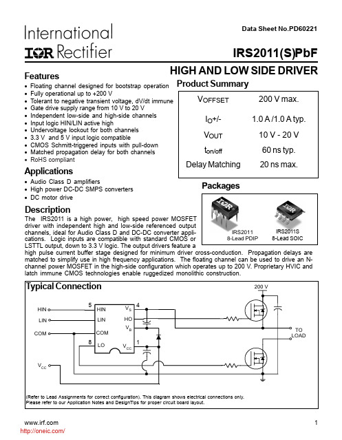
Features• Floating channel designed for bootstrap operation • Fully operational up to +200 V • Tolerant to negative transient voltage, dV/dt immune • Gate drive supply range from 10 V to 20 V• Independent low-side and high-side channels • Input logic HIN/LIN active high • Undervoltage lockout for both channels • 3.3 V and 5 V input logic compatible • CMOS Schmitt-triggered inputs with pull-down • Matched propagation delay for both channels PackagesHIGH AND LOW SIDE DRIVERProduct SummaryV OFFSET 200 V max.I O +/- 1.0 A /1.0 A typ.V OUT 10 V - 20 V t on/off 60 ns typ.Delay Matching20 ns max.IRS2011(S)PbF 1Data Sheet No.PD60221Applications•Audio Class D amplifiers•High power DC-DC SMPS converters • DC motor driveDescriptionThe IRS2011 is a high power, high speed power MOSFET driver with independent high and low-side referenced outputchannels, ideal for Audio Class D and DC-DC converter appli-cations. Logic inputs are compatible with standard CMOS orLSTTL output, down to 3.3 V logic. The output drivers feature ahigh pulse current buffer stage designed for minimum driver cross-conduction. Propagation delays are matched to simplify use in high frequency applications. The floating channel can be used to drive an N-channel power MOSFET in the high-side configuration which operates up to 200 V. Proprietary HVIC and latch immune CMOS technologies enable ruggedized monolithic construction.IRS2011S 8-Lead SOIC IRS20118-Lead PDIP • RoHS compliantAbsolute Maximum RatingsAbsolute maximum ratings indicate sustained limits beyond which damage to the device may occur. All voltage param eters are absolute voltages referenced to COM. The thermal resistance and power dissipation ratings are measure under board mounted and still air conditions.Dynamic Electrical CharacteristicsV BIAS (V CC, V BS) = 15 V, C L = 1000 pF, T A = 25 °C unless otherwise specified. Figure 1 shows the timing definitionStatic Electrical CharacteristicsV BIAS (V CC, V BS) = 15 V, and T A = 25 °C unless otherwise specified. The V IN, V TH, and I IN parameters are refere to COM and are applicable to all logic input leads: HIN and LIN. The V O and I O parameters are referenced to COM an are applicable to the respective output leads: HO or LO.Lead DefinitionsSymbol DescriptionHIN Logic input for high-side gate driver output (HO), in phase LIN Logic input for low-side gate driver output (LO), in phase V B High-side floating supplyHO High-side gate drive outputV S High-side floating supply returnV CC Low-side supplyLO Low-side gate drive outputCOM Low-side returnLead AssignmentsFigure 1. Timing Diagram 分销商库存信息:IRIRS2011SPBF IRS2011PBF IRS2011STRPBF。
芯片型号汇总
PIC16C72A-I/SOPIC16F677-I/SS(密脚)PIC16F870-I/SPPIC16F886-I/SOPIC16F886-I/STPIC18F46K20-E/PTPIC18F6520-I/PTPT1301PT1301RF2126SD2200DLPISMA5102STG8203STK0460FSTPR1020CTSTPR1620CTTEA5767TIP49TIP49W19B320SBT9(代替型号W19B320ABT7H)2SA1266-Y2SA933AD7524JNZAP1507A T89C51RD2BS2F7HZ0194ABS2F7HZ07395CS5460-BSZDG211BDJEPM7064SLC44-10NEPM7064SLC44-10NK1118LPC2136FBD64MAX6103EURMJE5731AGMP2601MP7720MP7720MP7722MP7782PIC12C672-I/SNR5402N101KDREF3030AIDBZREF3030AIDBZS9013S9013S9015S9015SB8100SN74LS595NSTC89C55RD+40C-P TL3842TL3842TLC2543CNTLC2543CNTLC549CPTN2124K1TYN267PTYN267PX5045PZ48637407805080508050805080508050855085508550855085508550SB2401N40071N4747A-G1N4748A-G24M晶振2N90C2SD4662SN36324128BWP6N1366N13674LV59578L0578L05AD524ARAD524ARAK4645AMS1117-3.3V BC807DM-25-7 BH6799FVM-TR BS108BSM15GP120-B2 C8051F330DCA T1025JI-30CA T6219-33CR2LS-30DNY380PNDPA1870DPA423G DSPIC30F2010 DSPIC30F4012 ES1DESD5B50ST1G FAN2011EMPX FQPF8N60CG3JGBPC3508W GBU8DGTM900BHCF4201M013TR HER308HER308HMC287MS8HV9931LGIC7107IP101AIR2520DIRF730IRF740IRF830IRF840ISL9R1560PF2J2-Q06B-GKBU6JKBU8JLM1086-3.3VLM2576-5VLM4040AIM3-5.0LP3966ET-ADJLT1013LT1085CM-33M25P64-VMF6TP M88C200MAX3072EESA MBR1040MBR2045MBR30100CT MBR30100PTMC33981BPNAMP1029EM-LF-Z MP1029EM-LF-Z MP1410ES-LF-Z MP1482MP1488MP1488DJ-LF-Z MP1519DQLMP1540MP1580HS-LF-Z MP1953DN-LF-Z MP2105DJ-LF-Z MP2259MP2481MP2602DQ-LF-Z MP3202DJ-LF-Z MP3202DJ-LF-Z MUR820GMUR860GMUR860GNCP1014ST100T3G OP290GPCF2128PIC10F204T-I/OT PIC10F206T-I/OT PIC12C508-04/P PIC12F629-I/PPIC12LC509APIC16C72A-I/SO PIC16F688-I/SL PIC16F883-I/SO PIC16F886-I/SO PIC18F4680-I/P PIC18F46K20-E/MLPS1010RPS106RPS12046PS12046PT2256RL207(国产/进口)S20C40S80833CNUASAK-C504-2E24 SKRBAAE010 SKRBAAE010SLA7026MSLA7026MSLA7033SMAJ150ASP1110SP3232BEASS32STP2NK100ZSTP2NK90ZT6316ATD62003APTDA7396TNY278PNTNY278PNTOP222YTOP222YTPS71533DCKRTWH8751UAA3595HN/C3UC3844UF306ULN2803AGUTC3308VIPER53ZS3051212085S29AL016D70TF1010 2N30552N40332N62462SC26252SC26252SC40832SK1334BYTL-E2SK14112SK2334ST60EPF06PBF60EPF06PBF75333P7MBP75JB060-01A2611DAE2501BAME8800BEETYAME8800MEETZAN7815AP3700ZTR-E1B0530WS-7-FBC141BCR1AM-12ABL182LBQ24070BS170BSM15GP120-B2BTA2112-600BBTA2112-600BCP2102CS4344CZZCS8900AIQ32/CQ32 CXA2075DB3E2023ECWV1334KC9ED03EMD812EMP812FM1072LPFMQ-G5GSFS3KM-10AFS5KM-10AGS3J-BGT50J101HT2015-PLHT9032CHWD2109IHLP2525C2EBR47M01 IHLP2525C2EBR47M01 IP101A-LFIRF9140NIRFU9024NIRL2203NIRLML6401J2-005B-GK4M51323PC-DG75 K4M51323PC-DG75 k4s561632h-uc60K9G8G08KBpc25005-gKDT1304KSB1151YL6569L6569L6599DLA7213LA7213LD7550LM4853MMLMC7101AIMLP2985-18DBVR LT1615LTF5022T-3R3N2R5 MASWSS0115 MBR0530MBR2545PTMBR2545PT MBRB2045CTMC3403PMCP2551T-I/SN MCP9800MJE172MJE172MJE172MJE182MP1518DMP1583DSMP1593MP2259MP2363MP2363MSP430F223IRHAR MUR440NDC7002N-NCopa348a1dckrPCM1772PWG4PESD3V3L1BApi2259PIC12F509PIC16C433/JWPIC16F688-I/STPIC16G630-I/PPIC18F2420-I/MLPIC18F4321-I/PTR1114Q331r1130h001c-t1R3112N251ARE200BRGP30JRSOP36230TRS6A0073X01-C0CXS812C33S87C752-5A18S87C752-5A28SC0603C220M05SKN2000/03SLF6028T-4R7M1R6-PEsn74ahc1g00dcksn74lv1g06dckSPHE8202Lss14SST39VF6401B-70-4C-EKE STP140NF75STP140NF75STP40NF10STP40NS15STP8NF55-06STPS2060CTSTPS20S100STRX6757STTA3006PTA8440TDA7266PTDA8560QTDA8560QTDA8571JTDA8920BJTEA1761TTG35C60THX208TIC246MTLV1117-33CDCYRG3 TM9926TM9926FSTN6R04-H-ETOP200YATPA8920BTHTPA8920THTPS62000DGSTRLML2502TSC2003TSOP36230TRTSOP36230TRTWH8778UC3573NUC3573NUR5596VI-JW2-CZWM8731YDS-305YPPD-J001YPPD-J014AYPPD-J014BYPPD-J015BYPPD-J016BZTX65112-215SYGC-S530-E1/TR8 19-217/S2C-AM2N2VY/3T 25LC040T-I/SNAMC7150BA T54S-7-FBZX84C6V8LT1CA T809FDC6000NZFHP3130IS5XFHP3230IMU8XFUSE-5AHER207IP4035CX24IP4041CX25IRLM6401TRPBFIRLMS2002TRPBFLMH6639MF/NOPBLTC1872ES6LTC1872ES6MBR0520LT1GMBR0520LT1GMBRA210LT3GMCP1702T-3302E/CB MSP430F2111IPWRPT4115S-80930CLMCSB240SP6201EM5-L-3.3/TRSP6201EM5-L-ADJ/TR SP6205TPS61030RSATVP5146PFPTVP5146PFP10V 1500UF16V 3300UF19-217-R6C-AM2P1VY-3T 2MI100F-0252MI50S-0502SC19706.3V 1500UF6.3V 2200UF6.3V 3300UF6N1376N1376N13774HC138D74HC245D7MBR50NF060A TMEGA48V-10PUBTA12-600BCS9803GPD304XF20U40DNFDFS6N754-NLFODM121R2IN5822KA5M0765RQCTUMBR20H200CMCF5212CAE66PA42PIC12F683-I/SNPIC16C57C-04/PPIC16F677-I/SOPIC24FJ256GA110-I/PT PM15CMA060SC9803GPSIA0903X01SKD31F/16SKD31F/16SSG8205ASTP4NM60TIP41CTL494CVUB60-16N0116F74-I/P1NC452N602SD16102SK26112SK26112SK28372SK283739SF020A-70-440TPS125420(压力传感器)5651(压力传感器)5652(压力传感器)5L0380R67F110(温控开关)67F110(温控开关)6MBI50S-12074HCT540DB75333PADF-2-1ADF-2-1ADF-2-1ADNS-2610(传感器)AI325AMC7135AMC7135A T90PWM3-16SQA T90SC7272CA TMEGA128-16AUA TMEGA128-16AUBC182BBC212BBCR8PM-14LABL8553-33PRMBS2F7HZ0194ABS2F7VZ0194-BS2F7VZ7395 BSM50GB120DN2BSM50GB120DN2BSM50GB120DN2BT169BTA140-800BTA140-800C1815C945CP10TD1-24ACP157D1-24ACSC9270D1D40D304XD304XDS12C887DS12C887DS52502DSPIC30F3013-30I/SOE13007F12C20CFDS6898AZFJA13009TUFQPF10N60CFQPF6N80CFS450R17KE3FS450R17KE3FS8205AFS8205AGU1GHEF4069UBPHT2015-LQHT2015-LQHWD4863HWD809ICL7612DCPAICL7612DCPAIN4764AIN4764AIN4764AIP4035CX24IP4041CX25IRF7750TRIRF9540NIRF9540NIRFZ24IW1692K3113KA4558SL6565L6565LC863324A-5S68LC863528C-55LOLM1237BDKC/NA LM311PLM317BTLP2981ATM5-3.0LT1249CN8LT6233MB6SMBR10H200MBR20100MBR2045CTGMC33262PMCP4023T-103E/CH MCP4922-E/PMCP9800AOT-M/OTG MCR100-6MCR100-6MFRC500MGSF1N03LT1G MOC3061MP1411DH-LF-Z MPX5010DPNR12S5/500PCM2900EGPIC12F683-I/PPIC16F877A-I/LPM30CTJ060-36PSD35/16RB521G-30RB521S-300.075RT8008-18RBRT8008-18RBS29GL032N90TFI030 SBL1545CTSD0418ASISG6849-65DSG6849-65DSKKT250/14ESKKT250/14ESKR71/16SP1110SP1117-1.8SP2110SSG50C60SSG50C60STP6NK60STPR1620CTSTPS3045CWSTRF6652STRF6652STRF6652TA2003PGTA2003PGTAP476K016SCTDA9886TSTHC63LVDF84B THX202TOP254YNTOP254YNU1560VIPER12ASWFF7N60WFF7N60XC2S100-5TQ144C YDS205YPPD-J015BYPPD-J018E05NL03LA178487-120N60S520N60S52DI300A-050D2SC50472SC50473P4MH403CNQ1004921QP1018AAA T3155ITP-T1AM9945NAO4803AAPT5010LVRAXK5F26547AXK6F26547BA V70LT1GCBC3225T100KR CBC3225T220KRCD3610CS9803GPDAC712UKEL817CEPM3256AQC208-10N EPM3256AQC208-10N ERA-1FDV303NFDV303NFSDL0165RNFSDM311FSDM311FSUSB30MUXGL827HA17358HD4066BHN27C101AG-15IR2520DIR2520DIR2520DIRF1045IRF2805IRF3805IRFB4227PBFIRFB4227PBFJM20316K4M51323PC-DG75 KA78T12TUL6563L6599DLD7575PSMC3PHACVPEMI1320MI1321MOC3063MST726C-LFNDC7002NNTJD2152PT1G NTJD2152PT1GPIC10F200TPIC18F242-I/SP PMWD20XNPS22056RM600DY-66SS6A0073X14-COCX SMAJ6.0ASN75LBC174NST330C16COST330C16COSTB10NB50STB10NB50STP12NM50FPSTP9NK50ZSTPS1L40ASTTH2L06STW20N60TC4011BFTC4451VPATCM809JENB713 TDA7439DSTDA7439DSTFBS4650-TR3 TFBS4650-TR3TL082CDTTL084CNTNY266PNTOP244YNTS3USB221DRCRG4 TSC2003VU034-18N01YDS512YDS512YPPD-J001AZ0103MNZ0103MN901316F872-I/SP16F872-I/SP16F873A16F873A2MBI200N-0602SK26116MBP75RS1206MBP75RS12074HC59574LS244A940AM9945NAM9945NA TA5428CM0565RCM0565REL817EPM570GT144C4 EPM570GT144C4 FS9922GWS6967IRF460KA5H0380RYTU LD7575LM117KLM358LM385B12LP2950ACZ-3.3G LP2950ACZ-3.3G MP2259DJ-LF-Z MP2359MUR3060PTNCP1575NCP1653APG/ADR PS21246-EPS21255-EPT4105CRHRP8120S8550SBC337SBC337-25SKIIP31NAB12T16 SLA6026SN75LBC174NSR160TB1334FBTB1334FGTOP254YNTOP255YNUC3842BW5100WFP50N062SA812M62SA812M72SB6242SB772P2SC1623L62SC1623L72SC2712GR2SC3356R242SC3356R252SC3357RE2SC3357RF2SC4226R242SC4226R252SD772P2SD882P74LVCH162245ADL 74LVCH162245ADL 74LVCH16245ADL A1156-YA1156-YA1270-YA1270-YAA T3155AD8300ANAOT430B560CBAS21DW-7FS7M0880TU GBPC3508HIT647-EQHIT667-EQHTC78L05KA1L0380RBTU KA1L0380RBTU KBJ406KBJ410KBJ410KRC1055KSP10BUKST10MFTLC863328A-5T46LC863328A-5T46LTC3406ES5LTV350QV-F04M430V138TNE555NPMBT4401PMBT4403PS2501-1-A-KKPS2501L-1-E3-A-KK/L QM30HC-2HSKR240/16THX202HTJM4558CDTTLP281-4YG225N471061.5KE13CA1D600A-0301D600A-0301N47331N474424AA64-I/SN24AA64-I/SN28SF040A65HVD308267L09003466D115A-0506D115A-05074LVC14APW74LVC14APW75645P82C55AD7846JPADM705ARZAM188ES-20KCAO4842LAPW7060KC-TRL BYV26EBYV26EC945CH372ADAC0830LCWM DAC8412FPCEPM3032ALC44-10 EPM7128ELCES6628FFDS6912FDS6912HER153HER153HWP2171IR2103IS62C256AL-45 ISR154-600JW1FSN-DC12V JW2SN-DC12VKA3525ADKSB772KSB772YKSB772YKTB2955-O-UKTB2955-O-ULM318LM714M50195M50195M50195MAX7129ACPL MC145102PMC145102PMC33204DMCPS08AW16CFU MPX5100DPMT88E43BSMX26L6420MC NRF24L01PA92PIC16F630T-I/ST/SL PT7A6632JSAB80C537SARS01V01SG5841DZSII9013CLUSII9030CTUSPD03N60C3STP6NK60ZFPSTS2300SSTS2301STS2307TCD1304DGTCD1304DGTLP114TP3465TPC8107VLA517VLA517W27E010-702SC3320A04842LBYV27-200D17P149CTD20LC40D92-03MUR110RLMUR3040NCP1207PNW6005ASPIC24FJ64GA002-I/ML SP6013ASTB36NF06T2-1T-KK81TL494CNTPS79101DBRUC3842BN2SD1781KT146R74HC595DBCR3KM-12RAHEF4066BPL7905LM324NMDC100A1600VMIC29302BTSCN-3-28SN75176BPTLC7528CNYG225C2YG225N4YG255N215V-D12061N414825LC1282N22222N22222N29073656AG3DD15D6CWQ06FN6CWQ06FNA3120A3120AD7863BR-10AD8531ART-REELADM705-ARZAPXA200ARA220MF55G A T89S52-24JUA T89S52-24JUBAS16BTS660PE3180ABU9431-C1CD1206-S01575CL6012XCL6012XEL817B-SFM24C04A-GFQU13N10LFQU13N10LFR107FR107GL827HER307IRF5305IRS2168DJ174J174J175J175J175K9F2G08R0A-JIBOKIA431AKIA431BKSD1691L358L358LM3845MMMAX3072MAX491CPDMBT35200MMBTA44-400V-300mA MP1482MP1482OV9650-KL1APC929PIC16CE625-04/SOPT70302S6A0073X14-COCXS6A0073X14-COCXS6A0073X14-COCX SAB82352HSARS01V1SF5408SH3750ASH3750ASLA7026MSMAJ4735ASMAJ4744ASR3100STM32F103VETSTP10NK70ZFPTHX203HTL431TL594CDRTL594CDRTPS5430DDAG4TPS72301DBVRUF1004CTUF1004CTUGSP08JXC3S1000-4FT256I1N457A1N938B-1JANTX2068DD2SA812M62SA812M72SB772P2SC1623L62SC1623L72SC2712GR2SC33552SC3356R252SC4226R242SC4226R252SD882P455E5L0380R830BA2624A3901A3901SEJTR-TA T17C128BA6220BF247BBJ8P153ABJ8P153ABJ8P508ABJ8P508ABQ2054BSM100GD120DLC BSM100GD120DLC BTVZ0502SABZT52C10-7C8051F120CD3620CD4067CD4067CS3310CS3310DAN202KDAN202KDP104CDS2433DS2433DTB114ESDTC144EKADTC144EKADTC343TSEL817BEL818CEM78P153SEM78P156ELEM78P156ELEM78P156NEM78P156NEM78P447SEM78P447SEM78P458AEM78P458AEM78P803A/BEN25F40-100GCPEN25F80EV1527FHP3230IM8XGBU25AGRM55ER72A475KA01L HCPL2530HCPL-2531.SHIT647-EQHIT667-EQHT1380HT1381HT1620HT1621HT1621BHT1621GHT7130HT7130HT7133HT7133HT7136HT7136HT7144HT7144HT7150HT7150HT7530HT7530HT7533HT7533HT7536HT7536HT7544HT7544HT7550HT7550HWD2171HY5DU121622CTP-D43-C ICP-N38ISS86ISS86ISS86J174J174J175J175J176J176J177J177JCS830CKRA105MKSP2222KST10MTFKTC9014CL78L05AC2LG9110LM2575T-5LM324LM324LM3475MFLM3485MMLM3658SDLM4562NALM567CHLNK501PNLTC5505-1ES5MAX491CPDMAX706CSA-TMC145010DWMC145010PMC145012DWMC145012PMC145018PMC56F8323VFBEMCP1726-1202E/SNMCP2030-I/SLMJL4281AGML4803MLC3100AMMBT5401MP1410ES-LF-Z MP1411OV2610PAN3101PIC18LF4682-I/PT PMBT4401PMBT4403PP25-48-15PTFA192001ERV4145ANS5C-225HVSA9259SAB80C166-MSB10100FCTSD2200DLPISM2845SS8050CBUTB2132FNTB2132FNTB62705FNTC9274N-011TJM4558CDTTLC5510AITM9936TOP210TV00570002CDGB VIPER53DIP-E WM8768GEDS WM8768GEDS 7805780678087809781278157824790579067908790979127924130031300574HC0474HC13874HC16474HC24574HC59578M0578M0678M0878M0978M1278M15A940A T1628/AM1628 B772BD242CBD243CBD244CBT131-600BT134-600EBT136-600EBT137-600BT137-600EBT138-600EBT151-500RBT151-500RBT152-500RBT169DBTA06BTA08BTA12BTA16BTA26BTA41BTB04-600SL BU406C106DC2073CD40106CD4011CD4011CD4052CD4053CD4066CD4541BNCD6282CD6283CD9088CS4334CT502D880D882E13001AE13005AE13005AE13005AE13007AE13007AEV1527FM62429GT2300/2301/2302 GT3400/GT3401 GT4953GT8205GT9435GT9926HT1380HT1621BHT1628HT6221HT6222JRC4558DKA3525KA3842KA3842/UC3842 KA3843KA3845KA7500KA7805KA7806KA7808KA7809KA7812KA7815LM2575LM2575T/SLM2576LM2576T/SLM258LM2596LM2596T/SLM2901LM2901LM2902LM2902LM2903LM2903LM317MLM317TLM324LM324NLM339LM339NLM358LM358NLM393LM393NLM567MAC97A6/8MCR100-6MCR100-8MUR1660CTNE555POP07PL2303PT2262PT2272TDA2003TDA2030ATDA2030ATDA2822M/(6-15V) TEA2025B/(9-15V) TIP122TIP127TIP31CTIP32CTIP41CTIP42CTL494TYN612UC3843UC3845ULN2003ULN2803UTC2003LUTC339X0405MFX0605MFZ0103MFZ0607MF0802A字符LCD液晶显示模块0802B字符点阵模块12232-4液晶模块12232-9中文3V液晶显示模块12232A液晶模块12232B图型点阵模块12232C点阵模块128128图型显示模块12864A图型显示模块12864A液晶12864C图型点阵模块12864C中文点阵模块12864I低功耗汉字显示液晶模块12864T液晶模块/LCM模块/液晶屏(图) 12864点阵图型液晶模块T6963C1601A大字符显示模块1601字符显示模块1601字符液晶模块1602大字符点阵显示模块19264A蓝白/黄绿液晶模块19264A蓝白液晶显示模块19264B图型点阵液晶显示模块2×10中文字库液晶显示模块240128-1显示模块240128A蓝白模块240128A液晶显示模块240128点阵液晶模块240128中文字库点阵显示模块/液晶屏24064A图型液晶/LCM模块2864I-1中文点阵液晶模块/LCM模组3.5寸液晶显示屏320240C图型点阵模块3V低功耗0802A字符模块3V低功耗字符点阵3V图型点阵12832中文LCD3V图型点阵160128A显示模块4.3寸夏普彩屏4004A字符液晶模块402A两行大字符模块COG240128C低功耗模块LCD/LCM12864-1液晶显示模块LCD/LCM240128-1点阵图型模块LCD/LCM5.7寸320240A高亮液晶LCD/LCM液晶404ALCD/LCM英文液晶显示模块LCD12232-2液晶模块LCD12832A显示模块LCD12864-06模块LCD12864-07模块LCD128645显示模块LCD12864D液晶显示模块LCD12864J字库模块LCD1601A点阵字符模块LCD1601字符显示模块LCD1602大字符显示模块LCD1604液晶模组LCD大字符1601显示模块LCD点阵显示模块12232-1LCD液晶LCD液晶模块LCD液晶显示模块LCD液晶显示模块128641LCM12864-7点阵显示模块LCM161点阵模块LCM192641点阵图型模块T6963C控制芯片液晶12864F串口中文两行液晶模块/3V显示屏串口字库/图型LCD液晶显示模块低功耗12232F中文图型点阵显示模块(图) 低功耗液晶显示模块两行字符点阵模块三星LTV350QV-F04显示湿度计LCD液晶液晶12232-3显示模块液晶屏3.5寸带触模液晶显示240128A模块字符162液晶显示模块字符204点阵显示模块字符点阵0801B模块字符模块2002A点阵40021N40071N4744A1N581925AA1024-I/SM2SC1946455EADM705-ARZBSM100GD120DLC BSM100GD120DLC BTA20BTA204S-600D BTVZ0502SACM75YE13-12FCM75YE13-12F DAC0832LCNDS2433DS2433DSA17-16AESM6045DVESM6045DVEV1527FDC37C78-HTGBU25AHC08HC08HER204HER204ICP-N38IMBH75D-060S IRLZ44AIRLZ44AISS86ISS86ISS86J174J174J175J175J176J176J177J177KRA105MLM2575T-5.0LM2576T-ADJLM2576T-ADJLM2595S-ADJLM2595S-ADJLM2596T-ADJLM2596T-ADJLM567CHLP8345CLD-1.8 LS14LS14MAX491CPD MAX491CPD MCP2030-I/SL MP2365DN-LF-Z NCP1014ST65T3G NS0013LFP4KE51AP4KE51AP4KE51APL2303HXPL2303HXPL2303HXPL2303HXPL2303HXPL2305PL2305POS-100PS12036PS12036PT76S16ART9164CMS3C2410ALS3C2410ALSA8281IGSA8282SAB80C166-MSB10100FCTSB2040FCTSB2040FCTSD2405APISM0038SPHE8202RQSPIF225A-HL231 SS26T3GSS26T3GSS26T3GST6368B1/FEMST6368B1/FEM STC352TA2132TA2132TB2132FNTB2132FNTB62705FNTL494CNTMG8E60UM3750AVIPER53DIP-EWM8522GWM8768GEDSWM8768GEDS YDS212YDS21278057809130011300320100160L2C43A16V/680UF22UH24C0229GL512N11TAI010 2KDB08M2SA1349/2SC3381 2SD1835S2SD1835S-AA2SK1172SK1173224G-1-100E3314R-1-203E400V/10UF4921QP1002B4921QP1009A4921QP1017A4921QP1043B4921QP1043C4921QP1046A4921QP1047A74HC16475NF7578L0578L0578L088202TAD620ARAD8620BRADTL2-18AP4313KTRBD9703FP-E2BD9703FP-E2BL8023BL8506-42CSMBN/53SBS170CM2020-00TRCP10CS3310-KPD1555DB107DM0465RYDTUDS1620DSPIC30F4013EM78P152ANEN25F40-100GCPFDN340PFF501FM1105GBLC03GBLC03HER207HMMC3124HMMC3124HY5DU1216DTP-D43-C IN5819INA106UINA128UINA128UAISD2560PITR8307/S18ITR8307/S18 ITR9909J112J112JRC4558JZ6206(3.3V) JZ9261(5.0V)K3435KA378R12KA7500KA7500KBP204GKBP204GKBP206GKBP208LAN9115-MT LM2575T-5LM324LM339LM358LM386LM393LM94021BIMG LT11293LTC3703EGM27C512-12F1 M81C55A-2 MAX232MAX3221EEAE MBI1802MC34064A MDSR-7 MDSR-7MIC2951-02YM MP1517DR-LF MT1389QE-K NE555OP27FZOPA2132OPA2604PC817PS21867RJ23N3ABOPT RK3055ERTL8102ELS29GL064A90TFIR4S3P9234XZZ-COC4S3P9234XZZ-COC4S8261AAJS8261AANS8261ABPS8261ABZS9013HSA8281SA8281SPHE8202RQ/TQSPW20N60S5SST89E516RD-40-C-PIE SSU2N60BSTPS2045CTTDA2822(6V)TEA2025(9V)TL431(+-0.5%)TL431ATL494TL494TSOP2136UC3842UDZ5V6BUSBN9603-28MVIPER12AVIPER22AXC1736EPC103653-1103653-120JL2C20JL2C6MBI20GS-0606MBI20GS-06074HCT14D93C46AAH180-WG-7A T89S51-24AU/AIA TMEGA48V-10MUA TMEGA48V-20AUA TMEGA48V-20AUA TMEGA8-16AUA TMEGA8-16AUA TMEGA8-8AUA TMEGA8-8AUCA T1025JI-30CA T1025WICD1691CBCD1691CBCD1691CBCD74ACT20MCMQ82C55AZCMQ82C55AZCS9803GPD71055GBD71055GBEPM3256AQC208-10N FM24CL16-GFM24CL16-GFM24CL16-GFM25L256BGGP30MGP30MHCF4017BEYHCF4017BEYHCF4060BMHCF4060BMHMC284HMC484HMC574MS8ETRHV9931ISP2032A80LT48ISP2032A80LT48KIA7806APKIA7806APLM8V302LM8V302LMX2531LQ1778 LTC3200-5LTC3200-5LTC3200-5M29W128FH70N6E MAX942MBRM140TMBRM140TMBRM140TMC1413BDGMC1413BDGMC68SEC811E2FN MC68SEC811E2FN MIG15J503HMIG30J501LMIG30J503LMP7731DF-LF-Z MT6225ANCP1395APGNJU9202BMNTJD4401NT1ON4742P06P03LVGP6KE24APLS-2PS11035PS11035QS3257QS3257R3111H481C-T1-F SAB80C537NSAB80C537NSN74HC74QPWRQ1 SP3232ESPX1117M3VC0568-V33-LF YPPD-J016BYPPD-J016E13009130091N458A24BC022SB6492SD6693296W-1-1013296W-1-20274HC14N74HC245N74HC37388W8010-NNB188W8510H-BAN1 88W8510H-BAN1 89C2051-12PUAH1802-WG-7AH180-WG-7AM29LV040B-60RJI BN/54SCD4529BECS4334DG442DYZDG442DYZDSE130-06AEM78P468NBQJ HCPL2530IN5817IN5817IN5817IN5820IRF7105IRS2186STRPBF KRC231SM27C512-10F1 MAX610CPANJM0302NJM0302NJM13700MNJW0281NJW0281NL17SZ74USPCF8574PPS1010RSRC4558IDRSB240SGH80N60UFDSI3018-F-FSRSR260TAS3204PAGTDA7535TJM4558CDTTL7705ACPTOP257YN13005MD2.0V稳压管2.0V稳压管2SA20942SC2712GR2SK27172SK3483-Z2SK38784921QP1023A4921QP1023A500欧可调电阻500欧可调电阻6MBP100RD060-01 6MBP100RD060-01 8302(HX3021)AD620ANA T29C512-12JCAU6331BA V99BC847BBC847BBC847BBUL38DBUL38DBUL58DBUL58DBUT11AC8051F023C945GCM2020-00TREN25F16ESD5B5.0ST1G FQPF5N80FQPF6N80FS3KM-10AFSBB20CH60FSBB20CH60 FSCM0765RGWDTU FSQ100FZT751FZT751HX3001(打LTWK) IKP20N60IRAMX16UP60A-2 IRFR120J5027-R(1.5A)J5027-R(2A)J5027-R(3A)KA3525AL149VL149VL6561/L6562LM556CMLMC555MA4820MC33179MCP1603T-180I/OS MCP1700T-5100/MB MCP6002-I/PMCP6002-I/PMP7782MPSA92MPSA92MS621FE-FL11EOV2640PC816PIC16F628APMBT4401/4403PS229QTF53BR1224N102H-TR-FR1224N102H-TR-F RFD16N05LRPS-2-30RY5W-KRY5W-KS29GL064A90TFIR40 SB20150FCTSI4425BDY-T1-E3SI4425BDY-T1-E3 SIA0903X01STA540SASTRX6757TC77-3.3MCTTR TDA2009TDA7266PTDA7266PTDA7266SATDA7375TDA7375TDA7377TDA7497TDA7497TDA7499TDA7499TJM4558CDTTLP521-3TMPZ84C011BF-8 TMPZ84C011BF-8TP0610K-T1-E3TP0610K-T1-E3TP0610K-T1-E3TP2808HCNTSF2N60MTVP5160U2352BU2352BUMB3NUMB3NUMB3NUMH3NUMH3NVR61F1250107N60S508-0559-0308-0559-0308-0559-03103308-611N120CND160NQ0825LC010AT-I/OT29F040-70LC2SA12202SC28902SC31332SC31332SD5532SJ19874LS53388E1011SA5-RCJ1C000 AC712AC712AD7711ARAHC164AO4828AOD442A T90SC7272CBC549CBCW72BTA41-700BBU406BW-S15W2+BW-S15W2+CM100DY-24HCM100DY-24HCM100DY-24HCNA30C101M-TMCS43L21-CNDSPIC30F6011A-30I/PT EEE2AA100UPFBC40LCFM1702SLGS-R51212HY5DU121622DTP-D43-C IR2161IR2161IR2161IR2161IR2161IRF3205IRFB17N50LIRKT105-16IRKT105-16IRS2186ISL9N312AD3ISO124PISO124PLM1086-3.3VLM224JLM318NLM3916NLM3916NLM3S615-IQN50LPC2132FBD64MBI1802MBR20100MC14093BCPMJ15003MJ15003MP1591DNMP1591DNMP1591DNMP1593DNMP1593DNMP1951DNMP3302DJ-LF-ZMRF166WMRF166WOM02OV9655PHE840MA6100MA04R17 RCV420AGRV5C348A-E2SD0418ASSKKT91/12ETA8127ATC77-5.0MCTTRTC77-5.0MCTTRTEA1098TVTM1618ATMS320LF2406APZA TNY254PUDN2983AUDN2983AV A7205CFWRA2412CS-1WWRA2412CS-3W1300513007130071300713009201002020025103.5251005472490001100UF/100V100UF/100V100UF/1W100UF/25V100UF/450V100UF/450V100UF/50V10UF/25V11-MD12716F887-I/P16V2200UF16v470uf173977-51N54081N5819218S4PASABG22UF/25V25N1202A233J2SC380-O2SC380-O2SD6492SD6692SK3485-Z-E2X80-DR230-S+35V1000UF4.3,1W4.3,1W40CPQ10040CPQ100470UF/100V47UF/16V47或,33UH68UF/400V6KA2474ALVC164245DGG 74LCX16245MTD 7914G-1-000E7914G-1-000E8N609N90A29L160ATV-70F ACT30BAD594ADAD7710ARZAD7710ARZAD8551ARAD8551ARAD8551ARAD96685TQAMC7150DLFTAMC7150DLFTAPM2301AR2001A T24C1024BA TMEGA8-8PUA TMLU810.46D.1,27G6346A AU6371AXK860145WGB1403NBA V23SBCM8011A2KPFBL8551BSM150GT120DN2BSM150GT120DN2BU52011HFVBUP314BUP314DC1815CD4514CM2020-00TRCP10TD1-24ACSC9270CSC9270CX4060CXD2498R13003DD313DF30FC-24DP-04VDFLS220L-7-FDS188B20DS1991C-FS+DSPIC30F3013-30I/SO DSPIC30F3013-30I/SODTV32DDTV32FEPM7128AELC84-10NEPM7128AELC84-10NER1004CTFMLG16SFMLG16SFMS6363CSXFP-20-1,27-60FPQ-100-0.5-10A FPQ-44-0.8-1G FQI16N60CFS10ASJ-2FSD210FSDL0165RNFT2232FTD2017G6K-2F-RF GBU8JGWS7301EHB9500HS108NHX3021ICX282AQINIC-1611LIR21592IR21592IR2233JIR2233JIRAMX16UP60A IRAMX20UP60A IRF014NPBF IRF014NPBF IRF014NPBF IRFP450IRFS9N60APBF IRFU320。
IRS27951STRPBF;IRS27951SPBF;IRS27952STRPBF;IRS27952SPBF;中文规格书,Datasheet资料
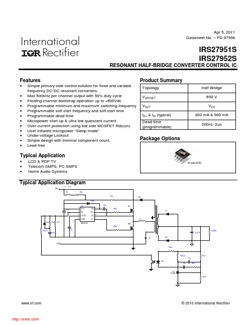
Apr 5, 2011Datasheet No. – PD 97556IRS27951SIRS27952S RESONANT HALF-BRIDGE CONVERTER CONTROL ICFeatures•Simple primary-side control solution for fixed and variable frequency DC-DC resonant converters.•Max 500kHz per channel output with 50% duty cycle •Floating channel bootstrap operation up to +600Vdc •Programmable minimum and maximum switching frequency •Programmable soft start frequency and soft start time •Programmable dead time•Micropower start-up & ultra low quiescent current•Over-current protection using low side MOSFET Rds(on) •User initiated micropower “Sleep mode”•Under-voltage Lockout•Simple design with minimal component count.•Lead-freeTypical Application•LCD & PDP TV•Telecom SMPS, PC SMPS•Home Audio Systems Product SummaryTopologyHalf-BridgeV OFFSET 600 VV OUT V CCI O+ & I O- (typical) 300 mA & 900 mA Dead-time(programmable)200ns~2us Package OptionsTypical Application DiagramDC BUSTable of Contents Page Typical Application Diagram 1 Qualification Information 4 Absolute Maximum Ratings 5 Recommended Operating Conditions 5 Electrical Characteristics 6 Functional Block Diagram 8 Input/Output Pin Equivalent Circuit Diagram 9 Lead Definitions 10 Lead Assignments 10 State Diagram 12 Application Information and Additional Details 13 Package Details 23 Tape and Reel Details 24 Part Marking Information 25 Ordering Information 26DescriptionThe IRS2795(1,2) is a self oscillating half-bridge driver IC for DC-DC resonant converter applications, especially the LLC resonant half-bridge converter. The frequency and dead time can be programmed externally using two external components. The IC offers over current protection using the on state resistance of the low-side MOSFET. The IC can be disabled by externally pulling the voltage at the CT/SD pin below its enable voltage threshold.Qualification Information†Qualification LevelIndustrial††Comments: This family of ICs has passed JEDEC’s Industrial qualification. IR’s Consumer qualification level is granted by extension of the higher Industrial level.Moisture Sensitivity LevelMSL2††† 260°C(per IPC/JEDEC J-STD-020C)ESD Machine ModelClass B(per JEDEC standard EIA/JESD22-A115-A) Human Body ModelClass 2(per EIA/JEDEC standard JESD22-A114-B)IC Latch-Up Test Class I, Level A (per JESD78A)RoHS Compliant Yes†Qualification standards can be found at International Rectifier’s web site /††Higher qualification ratings may be available should the user have such requirements. Please contact your International Rectifier sales representative for further information.†††Higher MSL ratings may be available for the specific package types listed here. Please contact your International Rectifier sales representative for further information.Absolute Maximum RatingsAbsolute maximum ratings indicate sustained limits beyond which damage to the device may occur. All voltage parameters are absolute voltages referenced to COM, all currents are defined positive into any lead. The thermal resistance and power dissipation ratings are measured under board mounted and still air conditions.SymbolDefinitionMin. Max. UnitsV CC Supply Voltage-0.3 25 VV B High-side Floating Supply Voltage-0.3 625 V S High-side Floating Supply Offset Voltage V B – 25 V B + 0.3 V HO High-side Floating Output Voltage V S – 0.3 V B + 0.3 V LO Low-side Output Voltage -0.3 V CC + 0.3 V CT CT/SD Pin Voltage -0.3 V CC + 0.3 V RT RT Pin Voltage-0.3 V CC + 0.3I RT RT pin source current--- 2 mA dV s /dt Allowable offset voltage slew rate -50 50 V/ns T J Operating Junction Temperature -40 150 °C T S Storage Temperature-55 150 R θJA Thermal Resistance, junction to ambient --- 150 °C/W P D Package Power Dissipation @ TA ≤ +25 ºC--- 833mWRecommended Operating ConditionsFor proper operation the device should be used within the recommended conditions.Symbol Definition Min. Max. Units V BS High-side floating supply voltage 10 VccVV S Steady-state high-side floating supply offset voltage -3.0†600 V CC Supply voltage 12 18 fsw Switching Frequency --- 500 kHz † Care should be taken to avoid output switching conditions where the V S node flies inductively below groundby more than 5 V.Recommended Component ValuesSymbol ComponentMin. Max. Units R RT RT pin resistor value 2 100 k Ω C CTCT pin capacitor value 200 2000pFElectrical CharacteristicsVCC=VBS=15V, VS=0V, CVCC=CBS=0.1uF, CLO=CHO=1nF, RT=50.5k Ω, CT=200pF and TA = 25°C unless otherwise specified. The output voltage and current (VO and IO) parameters are referenced to COM and are applicable to the respective HO and LO output leads.Symbol Definition Min Typ Max Units Test Conditions Low Voltage Supply Characteristics V CCUV + V CC turn on threshold 10.1 11 11.9 VN/AV CCUV - V CC turn off threshold (Under Voltage Lock Out)8.1 9 9.9 V CCUVHYS V CC undervoltage lockout hysteresis --- 2 --- I CCSTART V CC startup current--- 50 100 µAV CC = V CCUV+-0.1VI SLEEP Sleep mode V CC supply current --- 150 200 V CT/SD <V EN2, V BS =0V I QCC Quiescent V CC supply current --- 2 2.5 mAV EN1 < V CT/SD < 4.5VI CC46KHz V CC operating current @ f osc = 46KHz --- 3.1 4.5 RT=50.5k Ω I CC285KHzV CC operating current @ f osc = 285KHz---8.711RT=7.32k ΩFloating Supply CharacteristicsV BSUV+V BS turn on threshold 7.6 8.5 9.4 VN/AV BSUV- V BS turn on threshold(Under Voltage Lock Out)7 7.9 8.8 V BSUVHYS V BS undervoltage lockout hysteresis --- 0.6 --- I LKVS VS Offset supply leakage current --- --- 50 µAV B = V S = 600 V I BSSTART V BS startup current--- 50 100 V BS ≤ V BSUV+ - 0.1V I QBS Quiescent V BS supply current --- 50 100 V EN1 < V CT/SD < 4.5VI BS46KHz V BS operating current @ f osc = 46KHz --- 1 1.5 mA RT=50.5k Ω I BS285KHzV BS operating current @ f osc = 285KHz---5.77RT=7.32k Ω Oscillator I/O Characteristicsf SW Oscillator frequency44.346.648.9kHzCT=200pF,RT=50.5k Ω 271285 299 CT=200pF, RT=7.32k Ω V CT+ Upper CT ramp voltage threshold --- 5.0 --- V GBD V CT- Lower CT ramp voltage threshold --- 3.0 --- I CTSTART CT/SD pin startup current --- 10 --- µA V CT/SD < V EN1V RT Voltage reference at RT pin 1.92 2.0 2.08 V CM Current mirror ratio--- 1 --- A/A D Output duty cycle (LO and HO) 48 50 52 % t DTHigh/low output dead time170210250nsCT=200pFElectrical CharacteristicsVCC=VBS=15V, VS=0V, CVCC=CBS=0.1uF, CLO=CHO=1nF, RT=50.5kΩ, CT=200pF and TA = 25°C unless otherwise specified. The output voltage and current (VO and IO) parameters are referenced to COM and are applicable to the respective HO and LO output leads.Symbol Definition Min Typ Max Units Test Conditions Protection CharacteristicsR RTD RT discharge resistance ---115 ---ΩR CTD CT/SD discharge resistance --- 115 ---V EN1CT/SD rising enable voltage 0.75 1.05 1.4VV EN2CT/SD standby voltage 0.60.85 1.1V ENHYST CT/SD enable hysteresis voltage --- 0.2 ---V OCP Overcurrent VS threshold1.9 22.1VIRS27951 2.85 3 3.15 IRS27952t BLANK Leading edge blanking on LO --- 300 ---ns GBDt SD Shutdown propagation delay --- 300 --- GBD Gate Driver Output CharacteristicsV OH Gate High Voltage Vcc-1 --- ---VI GATE = 20mAVOLGate Low Voltage --- 0.05 0.15 I GATE = -20mAt r Output rise time --- 60 ---ns C LOAD=1nFt r Output rise time --- 200 --- C LOAD=4.7nF t f Output fall time --- 16 --- C LOAD=1nF t f Output fall time --- 65 --- C LOAD=4.7nFM DT Output deadtime matching|(DTLO-HO) – (DTHO-LO)|------25 nsI O+Output source current --- 300 ---mA GBD I O-Output sink current --- 900 ---R UP Pull up Resistance --- 20 ---ΩI GATE = 20mAR DOWN Pull down Resistance --- 3 --- IGATE=-20mA †GBD: Guaranteed by design.Functional Block DiagramInput/Output Pin Equivalent Circuit Diagrams:Lead DefinitionsSymbolDescriptionVCC Supply VoltageRT Oscillator timing resistorCT/SD Oscillator timing capacitor / shutdown COM GroundLO Low-side gate driveVSHigh-side gate drive return / HV current Sense HO High-side gate driveVBHigh-side floating supply voltageLead AssignmentsVCC: Power Supply VoltageThis is the supply voltage pin of the IC and sense node for the under-voltage lock out circuit. It is possible to turn off the IC by pulling this pin below the minimum turn off threshold voltage, V CCUV- without damage to the IC. This pin is not internally clamped.RT: Oscillator timing resistorThis pin provides a precise 2V reference and a resistor connected from this pin to COM defines a current that is used to set the minimum oscillator frequency. To close the feedback loop that regulates the converter output voltage by modulating the oscillator frequency, the phototransistor of an optocoupler will be connected to this pin through a resistor. The value of this resistor will set the maximum operating frequency. An R-C series connected from this pin to COM sets frequency shift at start-up to prevent excessive energy inrush (soft-start).CT/SD: Oscillator timing capacitor /ShutdownAn external capacitor CT from this pin to COM sets the dead time and frequency of the oscillator. The CT pin has sawtooth waveform, which is charged up by the current reference programmed at RT pin during rising slope and is discharged by an internal fixed 2mA current source during the falling slope. The falling time of the sawtooth defines the dead-time.At start-up, a 10uA current source charges this capacitor and the oscillator is enabled only when the voltage at this pin exceeds VEN1. The IC can also be used to enter sleep mode by externally pulling this pin below VEN2.COM: Logic and Gate drive GroundThis is ground potential pin of the integrated control circuit. All internal circuits are referenced to this point.分销商库存信息:IRIRS27951STRPBF IRS27951SPBF IRS27952STRPBF IRS27952SPBF。
ir2010

Features·Floating channel designed for bootstrap operation Fully operational to 200VTolerant to negative transient voltage, dV/dt immune ·Gate drive supply range from 10 to 20V ·Undervoltage lockout for both channels · 3.3V logic compatibleSeparate logic supply range from 3.3V to 20V Logic and power ground ±5V offset·CMOS Schmitt-triggered inputs with pull-down ·Shut down input turns off both channels·Matched propagation delay for both channels ·Outputs in phase with inputs ·Also available LEAD-FREEHIGH AND LOW SIDE DRIVERProduct SummaryV OFFSET 200V max.I O +/- 3.0A / 3.0A typ.V OUT 10 - 20V t on/off 95 & 65 ns typ.Delay Matching15 ns max.IR2010(S)(TR) & (PbF) 1Data Sheet No. PD60195-EIR2010(S)(TR) & (PbF)(Please refer to the Design Tip DT97-3 for more details).Note 1: Logic operational for V S of -4 to +200V. Logic state held for V S of -4V to -V BS .Note 2: When V DD < 5V, the minimum V SS offset is limited to -V DD.Recommended Operating ConditionsThe input/output logic timing diagram is shown in figure 1. For proper operation the device should be used within the recommended conditions. The V S and V SS offset ratings are tested with all supplies biased at 15V differential. Typical Absolute Maximum RatingsAbsolute maximum ratings indicate sustained limits beyond which damage to the device may occur. All voltage param-eters are absolute voltages referenced to COM. The thermal resistance and power dissipation ratings are measured under board mounted and still air conditions. 3IR2010(S)(TR) & (PbF)Dynamic Electrical CharacteristicsV BIAS (V CC , V BS , V DD ) = 15V, C L = 1000 pF, T A = 25°C and V SS = COM unless otherwise specified. The dynamic electrical characteristics are measured using the test circuit shown in Figure 3.4IR2010(S)(TR) & (PbF)Lead DefinitionsSymbol Description14 Lead PDIP 16 Lead SOIC (Wide Body)IR2010IR2010S Part NumberLead AssignmentsV DD Logic supplyHIN Logic input for high side gate driver output (HO), in phase SD Logic input for shutdownLIN Logic input for low side gate driver output (LO), in phase V SS Logic groundV B High side floating supply HO High side gate drive output V S High side floating supply return V CC Low side supplyLO Low side gate drive output COMLow side return 5IR2010(S)(TR) & (PbF)Figure 1. Input/Output Timing Diagram Figure 2. Floating Supply Voltage Transient Test CircuitFigure 3. Switching Time Test Circuit Figure 4. Switching Time Waveform DefinitionFigure 6. Delay Matching Waveform DefinitionsFigure 5. Shutdown Waveform Definitions(0 to 200V)HIN LINSDHO LOHV =10 to 200V<50 V/nsIR2010(S)(TR) & (PbF)Figure 8A. Turn-off Time vs. TemperatureFigure 8B. Turn-off Time vs. V CC /V BS VoltageFigure 7A. Turn-on Time vs. TemperatureFigure 7B. Turn-on Time vs. VCC /V BS Voltage Figure 7C. Turn-on Time vs V DD VoltageFigure 8C. Turn-off Time vs. V DD Voltage 7IR2010(S)(TR) & (PbF)Figure 9A. Shutdown Time vs. TemperatureFigure 9B. Shutdown Time vs. V CC /V BS VoltageFigure 10A. Turn-on Rise Time vs. TemperatureFigure 10B. Turn-on Rise Timevs. V BIAS (V CC =V BS =V DD ) VoltageFigure 11A. Turn-off Fall Time vs. TemperatureV CC /V BS Supply Voltage (V)IR2010(S)(TR) & (PbF)Figure 11B. Turn-Off Fall TimeDD Figure 12A. Logic 1 Input Threshold vs. TemperatureFigure 13A. Logic 0 Input Threshold vs. TemperatureFigure 13B. Logic 0 Input Threshold vs. V DD Voltage Figure 14A. High Level Output vs. Temperature 9IR2010(S)(TR) & (PbF)Figure 15B. Low Level Output vs. V BIAS VoltageFigure 16A. Offset Supply Current vs. TemperatureFigure 16B. Offset Supply Current vs. Offset Voltage Figure 14B. High Level Output vs. V BIAS VoltageFigure 15A. Low Level Output vs. TemperatureFigure 17A. Vbs Supply Current vs. TemperatureTemperature (C)Offset Supply Voltage (V)O f f s e t S u p p l y C u r r e n t (u A )IR2010(S)(TR) & (PbF)Figure 17B. Vbs Supply Current vs. V BS VoltageDDFigure 18A. Vcc Supply Current vs. TemperatureCC Figure 19A. Vdd Supply Current vs. Temperature 11IR2010(S)(TR) & (PbF)Figure 22. V BS Undervoltage (+) vs. TemperatureFigure 23. V BS Undervoltage (-) vs. TemperatureFigure 24. V CC Undervoltage (+) vs. TemperatureDD Figure 21B. Logic 0 Input Current vs. V DD Voltage6.07.08.09.010.011.0-50-25255075100125Temperature (°C)V B S U n d e r v o l t a g e L o c k o u t + (V )6.07.08.09.010.011.0-50-25255075100125Temperature (°C)V B S U n d e r v o l t a g e L o c k o u t - (V )6.07.08.09.010.011.0-50-25255075100125Temperature (°C)V C C U n d e r v o l t a g e L o c k o u t + (V )IR2010(S)(TR) & (PbF)6.07.08.09.010.011.0-50-25255075100125Temperature (°C)Figure 26A. Output Source Current vs. TemperatureFigure 25. V CC Undervoltage (-) vs. TemperatureBIAS GATE V c c U n d e r v o l t a g e L o c k o u t - (V ) 13IR2010(S)(TR) & (PbF)Figure 29. IR2010 Tj vs Frequency R GATE = 16 Ohm, Vcc = 15V with IRFBC40Figure 30. IR2010 Tj vs Frequency R GATE = 22 Ohm, Vcc = 15V with IRFBC30Figure 31. IR2010 Tj vs Frequency R GATE = 33 Ohm, Vcc = 15V with IRFBC20Figure 32. IR2010S Tj vs Frequency R GATE = 10 Ohm, Vcc = 15V with IRFPE50IR2010(S)(TR) & (PbF)Figure 33. IR2010S Tj vs Frequency R GATE = 16 Ohm, Vcc = 15V with IRFBC40Figure 34. IR2010S Tj vs Frequency R GATE = 22 Ohm, Vcc = 15V with IRFBC30Figure 35. IR2010S Tj vs FrequencyR GATE = 33 Ohm, Vcc = 15V with IRFBC20Frequency (Hz)Case OutlinesIR2010(S)(TR) & (PbF) Tape and Reel Details: SOIC8NC 17IR2010(S)(TR) & (PbF)LEADFREE PART MARKING INFORMATIONORDER INFORMATIONBasic Part (Non-Lead Free)14-Lead PDIP IR2010 order IR201016-Lead SOIC IR2010S order IR2010SLeadfree Part14-Lead PDIP IR2010 order IR2010PbF 16-Lead SOIC IR2010S order IR2010SPbF 16-Lead SOIC IR2010STR order IR2010STRPbFPer SCOP 200-002IR WORLD HEADQUARTERS: 233 Kansas St., El Segundo, California 90245 Tel: (310) 252-7105This product has been qualified per industrial levelData and specifications subject to change without notice. 9/12/2004。
芯片型号汇总

PIC16C72A-I/SOPIC16F677-I/SS(密脚)PIC16F870-I/SPPIC16F886-I/SOPIC16F886-I/STPIC18F46K20-E/PTPIC18F6520-I/PTPT1301PT1301RF2126SD2200DLPISMA5102STG8203STK0460FSTPR1020CTSTPR1620CTTEA5767TIP49TIP49W19B320SBT9(代替型号W19B320ABT7H)2SA1266-Y2SA933AD7524JNZAP1507A T89C51RD2BS2F7HZ0194ABS2F7HZ07395CS5460-BSZDG211BDJEPM7064SLC44-10NEPM7064SLC44-10NK1118LPC2136FBD64MAX6103EURMJE5731AGMP2601MP7720MP7720MP7722MP7782PIC12C672-I/SNR5402N101KDREF3030AIDBZREF3030AIDBZS9013S9013S9015S9015SB8100SN74LS595NSTC89C55RD+40C-P TL3842TL3842TLC2543CNTLC2543CNTLC549CPTN2124K1TYN267PTYN267PX5045PZ48637407805080508050805080508050855085508550855085508550SB2401N40071N4747A-G1N4748A-G24M晶振2N90C2SD4662SN36324128BWP6N1366N13674LV59578L0578L05AD524ARAD524ARAK4645AMS1117-3.3V BC807DM-25-7 BH6799FVM-TR BS108BSM15GP120-B2 C8051F330DCA T1025JI-30CA T6219-33CR2LS-30DNY380PNDPA1870DPA423G DSPIC30F2010 DSPIC30F4012 ES1DESD5B50ST1G FAN2011EMPX FQPF8N60CG3JGBPC3508W GBU8DGTM900BHCF4201M013TR HER308HER308HMC287MS8HV9931LGIC7107IP101AIR2520DIRF730IRF740IRF830IRF840ISL9R1560PF2J2-Q06B-GKBU6JKBU8JLM1086-3.3VLM2576-5VLM4040AIM3-5.0LP3966ET-ADJLT1013LT1085CM-33M25P64-VMF6TP M88C200MAX3072EESA MBR1040MBR2045MBR30100CT MBR30100PTMC33981BPNAMP1029EM-LF-Z MP1029EM-LF-Z MP1410ES-LF-Z MP1482MP1488MP1488DJ-LF-Z MP1519DQLMP1540MP1580HS-LF-Z MP1953DN-LF-Z MP2105DJ-LF-Z MP2259MP2481MP2602DQ-LF-Z MP3202DJ-LF-Z MP3202DJ-LF-Z MUR820GMUR860GMUR860GNCP1014ST100T3G OP290GPCF2128PIC10F204T-I/OT PIC10F206T-I/OT PIC12C508-04/P PIC12F629-I/PPIC12LC509APIC16C72A-I/SO PIC16F688-I/SL PIC16F883-I/SO PIC16F886-I/SO PIC18F4680-I/P PIC18F46K20-E/MLPS1010RPS106RPS12046PS12046PT2256RL207(国产/进口)S20C40S80833CNUASAK-C504-2E24 SKRBAAE010 SKRBAAE010SLA7026MSLA7026MSLA7033SMAJ150ASP1110SP3232BEASS32STP2NK100ZSTP2NK90ZT6316ATD62003APTDA7396TNY278PNTNY278PNTOP222YTOP222YTPS71533DCKRTWH8751UAA3595HN/C3UC3844UF306ULN2803AGUTC3308VIPER53ZS3051212085S29AL016D70TF1010 2N30552N40332N62462SC26252SC26252SC40832SK1334BYTL-E2SK14112SK2334ST60EPF06PBF60EPF06PBF75333P7MBP75JB060-01A2611DAE2501BAME8800BEETYAME8800MEETZAN7815AP3700ZTR-E1B0530WS-7-FBC141BCR1AM-12ABL182LBQ24070BS170BSM15GP120-B2BTA2112-600BBTA2112-600BCP2102CS4344CZZCS8900AIQ32/CQ32 CXA2075DB3E2023ECWV1334KC9ED03EMD812EMP812FM1072LPFMQ-G5GSFS3KM-10AFS5KM-10AGS3J-BGT50J101HT2015-PLHT9032CHWD2109IHLP2525C2EBR47M01 IHLP2525C2EBR47M01 IP101A-LFIRF9140NIRFU9024NIRL2203NIRLML6401J2-005B-GK4M51323PC-DG75 K4M51323PC-DG75 k4s561632h-uc60K9G8G08KBpc25005-gKDT1304KSB1151YL6569L6569L6599DLA7213LA7213LD7550LM4853MMLMC7101AIMLP2985-18DBVR LT1615LTF5022T-3R3N2R5 MASWSS0115 MBR0530MBR2545PTMBR2545PT MBRB2045CTMC3403PMCP2551T-I/SN MCP9800MJE172MJE172MJE172MJE182MP1518DMP1583DSMP1593MP2259MP2363MP2363MSP430F223IRHAR MUR440NDC7002N-NCopa348a1dckrPCM1772PWG4PESD3V3L1BApi2259PIC12F509PIC16C433/JWPIC16F688-I/STPIC16G630-I/PPIC18F2420-I/MLPIC18F4321-I/PTR1114Q331r1130h001c-t1R3112N251ARE200BRGP30JRSOP36230TRS6A0073X01-C0CXS812C33S87C752-5A18S87C752-5A28SC0603C220M05SKN2000/03SLF6028T-4R7M1R6-PEsn74ahc1g00dcksn74lv1g06dckSPHE8202Lss14SST39VF6401B-70-4C-EKE STP140NF75STP140NF75STP40NF10STP40NS15STP8NF55-06STPS2060CTSTPS20S100STRX6757STTA3006PTA8440TDA7266PTDA8560QTDA8560QTDA8571JTDA8920BJTEA1761TTG35C60THX208TIC246MTLV1117-33CDCYRG3 TM9926TM9926FSTN6R04-H-ETOP200YATPA8920BTHTPA8920THTPS62000DGSTRLML2502TSC2003TSOP36230TRTSOP36230TRTWH8778UC3573NUC3573NUR5596VI-JW2-CZWM8731YDS-305YPPD-J001YPPD-J014AYPPD-J014BYPPD-J015BYPPD-J016BZTX65112-215SYGC-S530-E1/TR8 19-217/S2C-AM2N2VY/3T 25LC040T-I/SNAMC7150BA T54S-7-FBZX84C6V8LT1CA T809FDC6000NZFHP3130IS5XFHP3230IMU8XFUSE-5AHER207IP4035CX24IP4041CX25IRLM6401TRPBFIRLMS2002TRPBFLMH6639MF/NOPBLTC1872ES6LTC1872ES6MBR0520LT1GMBR0520LT1GMBRA210LT3GMCP1702T-3302E/CB MSP430F2111IPWRPT4115S-80930CLMCSB240SP6201EM5-L-3.3/TRSP6201EM5-L-ADJ/TR SP6205TPS61030RSATVP5146PFPTVP5146PFP10V 1500UF16V 3300UF19-217-R6C-AM2P1VY-3T 2MI100F-0252MI50S-0502SC19706.3V 1500UF6.3V 2200UF6.3V 3300UF6N1376N1376N13774HC138D74HC245D7MBR50NF060A TMEGA48V-10PUBTA12-600BCS9803GPD304XF20U40DNFDFS6N754-NLFODM121R2IN5822KA5M0765RQCTUMBR20H200CMCF5212CAE66PA42PIC12F683-I/SNPIC16C57C-04/PPIC16F677-I/SOPIC24FJ256GA110-I/PT PM15CMA060SC9803GPSIA0903X01SKD31F/16SKD31F/16SSG8205ASTP4NM60TIP41CTL494CVUB60-16N0116F74-I/P1NC452N602SD16102SK26112SK26112SK28372SK283739SF020A-70-440TPS125420(压力传感器)5651(压力传感器)5652(压力传感器)5L0380R67F110(温控开关)67F110(温控开关)6MBI50S-12074HCT540DB75333PADF-2-1ADF-2-1ADF-2-1ADNS-2610(传感器)AI325AMC7135AMC7135A T90PWM3-16SQA T90SC7272CA TMEGA128-16AUA TMEGA128-16AUBC182BBC212BBCR8PM-14LABL8553-33PRMBS2F7HZ0194ABS2F7VZ0194-BS2F7VZ7395 BSM50GB120DN2BSM50GB120DN2BSM50GB120DN2BT169BTA140-800BTA140-800C1815C945CP10TD1-24ACP157D1-24ACSC9270D1D40D304XD304XDS12C887DS12C887DS52502DSPIC30F3013-30I/SOE13007F12C20CFDS6898AZFJA13009TUFQPF10N60CFQPF6N80CFS450R17KE3FS450R17KE3FS8205AFS8205AGU1GHEF4069UBPHT2015-LQHT2015-LQHWD4863HWD809ICL7612DCPAICL7612DCPAIN4764AIN4764AIN4764AIP4035CX24IP4041CX25IRF7750TRIRF9540NIRF9540NIRFZ24IW1692K3113KA4558SL6565L6565LC863324A-5S68LC863528C-55LOLM1237BDKC/NA LM311PLM317BTLP2981ATM5-3.0LT1249CN8LT6233MB6SMBR10H200MBR20100MBR2045CTGMC33262PMCP4023T-103E/CH MCP4922-E/PMCP9800AOT-M/OTG MCR100-6MCR100-6MFRC500MGSF1N03LT1G MOC3061MP1411DH-LF-Z MPX5010DPNR12S5/500PCM2900EGPIC12F683-I/PPIC16F877A-I/LPM30CTJ060-36PSD35/16RB521G-30RB521S-300.075RT8008-18RBRT8008-18RBS29GL032N90TFI030 SBL1545CTSD0418ASISG6849-65DSG6849-65DSKKT250/14ESKKT250/14ESKR71/16SP1110SP1117-1.8SP2110SSG50C60SSG50C60STP6NK60STPR1620CTSTPS3045CWSTRF6652STRF6652STRF6652TA2003PGTA2003PGTAP476K016SCTDA9886TSTHC63LVDF84B THX202TOP254YNTOP254YNU1560VIPER12ASWFF7N60WFF7N60XC2S100-5TQ144C YDS205YPPD-J015BYPPD-J018E05NL03LA178487-120N60S520N60S52DI300A-050D2SC50472SC50473P4MH403CNQ1004921QP1018AAA T3155ITP-T1AM9945NAO4803AAPT5010LVRAXK5F26547AXK6F26547BA V70LT1GCBC3225T100KR CBC3225T220KRCD3610CS9803GPDAC712UKEL817CEPM3256AQC208-10N EPM3256AQC208-10N ERA-1FDV303NFDV303NFSDL0165RNFSDM311FSDM311FSUSB30MUXGL827HA17358HD4066BHN27C101AG-15IR2520DIR2520DIR2520DIRF1045IRF2805IRF3805IRFB4227PBFIRFB4227PBFJM20316K4M51323PC-DG75 KA78T12TUL6563L6599DLD7575PSMC3PHACVPEMI1320MI1321MOC3063MST726C-LFNDC7002NNTJD2152PT1G NTJD2152PT1GPIC10F200TPIC18F242-I/SP PMWD20XNPS22056RM600DY-66SS6A0073X14-COCX SMAJ6.0ASN75LBC174NST330C16COST330C16COSTB10NB50STB10NB50STP12NM50FPSTP9NK50ZSTPS1L40ASTTH2L06STW20N60TC4011BFTC4451VPATCM809JENB713 TDA7439DSTDA7439DSTFBS4650-TR3 TFBS4650-TR3TL082CDTTL084CNTNY266PNTOP244YNTS3USB221DRCRG4 TSC2003VU034-18N01YDS512YDS512YPPD-J001AZ0103MNZ0103MN901316F872-I/SP16F872-I/SP16F873A16F873A2MBI200N-0602SK26116MBP75RS1206MBP75RS12074HC59574LS244A940AM9945NAM9945NA TA5428CM0565RCM0565REL817EPM570GT144C4 EPM570GT144C4 FS9922GWS6967IRF460KA5H0380RYTU LD7575LM117KLM358LM385B12LP2950ACZ-3.3G LP2950ACZ-3.3G MP2259DJ-LF-Z MP2359MUR3060PTNCP1575NCP1653APG/ADR PS21246-EPS21255-EPT4105CRHRP8120S8550SBC337SBC337-25SKIIP31NAB12T16 SLA6026SN75LBC174NSR160TB1334FBTB1334FGTOP254YNTOP255YNUC3842BW5100WFP50N062SA812M62SA812M72SB6242SB772P2SC1623L62SC1623L72SC2712GR2SC3356R242SC3356R252SC3357RE2SC3357RF2SC4226R242SC4226R252SD772P2SD882P74LVCH162245ADL 74LVCH162245ADL 74LVCH16245ADL A1156-YA1156-YA1270-YA1270-YAA T3155AD8300ANAOT430B560CBAS21DW-7FS7M0880TU GBPC3508HIT647-EQHIT667-EQHTC78L05KA1L0380RBTU KA1L0380RBTU KBJ406KBJ410KBJ410KRC1055KSP10BUKST10MFTLC863328A-5T46LC863328A-5T46LTC3406ES5LTV350QV-F04M430V138TNE555NPMBT4401PMBT4403PS2501-1-A-KKPS2501L-1-E3-A-KK/L QM30HC-2HSKR240/16THX202HTJM4558CDTTLP281-4YG225N471061.5KE13CA1D600A-0301D600A-0301N47331N474424AA64-I/SN24AA64-I/SN28SF040A65HVD308267L09003466D115A-0506D115A-05074LVC14APW74LVC14APW75645P82C55AD7846JPADM705ARZAM188ES-20KCAO4842LAPW7060KC-TRL BYV26EBYV26EC945CH372ADAC0830LCWM DAC8412FPCEPM3032ALC44-10 EPM7128ELCES6628FFDS6912FDS6912HER153HER153HWP2171IR2103IS62C256AL-45 ISR154-600JW1FSN-DC12V JW2SN-DC12VKA3525ADKSB772KSB772YKSB772YKTB2955-O-UKTB2955-O-ULM318LM714M50195M50195M50195MAX7129ACPL MC145102PMC145102PMC33204DMCPS08AW16CFU MPX5100DPMT88E43BSMX26L6420MC NRF24L01PA92PIC16F630T-I/ST/SL PT7A6632JSAB80C537SARS01V01SG5841DZSII9013CLUSII9030CTUSPD03N60C3STP6NK60ZFPSTS2300SSTS2301STS2307TCD1304DGTCD1304DGTLP114TP3465TPC8107VLA517VLA517W27E010-702SC3320A04842LBYV27-200D17P149CTD20LC40D92-03MUR110RLMUR3040NCP1207PNW6005ASPIC24FJ64GA002-I/ML SP6013ASTB36NF06T2-1T-KK81TL494CNTPS79101DBRUC3842BN2SD1781KT146R74HC595DBCR3KM-12RAHEF4066BPL7905LM324NMDC100A1600VMIC29302BTSCN-3-28SN75176BPTLC7528CNYG225C2YG225N4YG255N215V-D12061N414825LC1282N22222N22222N29073656AG3DD15D6CWQ06FN6CWQ06FNA3120A3120AD7863BR-10AD8531ART-REELADM705-ARZAPXA200ARA220MF55G A T89S52-24JUA T89S52-24JUBAS16BTS660PE3180ABU9431-C1CD1206-S01575CL6012XCL6012XEL817B-SFM24C04A-GFQU13N10LFQU13N10LFR107FR107GL827HER307IRF5305IRS2168DJ174J174J175J175J175K9F2G08R0A-JIBOKIA431AKIA431BKSD1691L358L358LM3845MMMAX3072MAX491CPDMBT35200MMBTA44-400V-300mA MP1482MP1482OV9650-KL1APC929PIC16CE625-04/SOPT70302S6A0073X14-COCXS6A0073X14-COCXS6A0073X14-COCX SAB82352HSARS01V1SF5408SH3750ASH3750ASLA7026MSMAJ4735ASMAJ4744ASR3100STM32F103VETSTP10NK70ZFPTHX203HTL431TL594CDRTL594CDRTPS5430DDAG4TPS72301DBVRUF1004CTUF1004CTUGSP08JXC3S1000-4FT256I1N457A1N938B-1JANTX2068DD2SA812M62SA812M72SB772P2SC1623L62SC1623L72SC2712GR2SC33552SC3356R252SC4226R242SC4226R252SD882P455E5L0380R830BA2624A3901A3901SEJTR-TA T17C128BA6220BF247BBJ8P153ABJ8P153ABJ8P508ABJ8P508ABQ2054BSM100GD120DLC BSM100GD120DLC BTVZ0502SABZT52C10-7C8051F120CD3620CD4067CD4067CS3310CS3310DAN202KDAN202KDP104CDS2433DS2433DTB114ESDTC144EKADTC144EKADTC343TSEL817BEL818CEM78P153SEM78P156ELEM78P156ELEM78P156NEM78P156NEM78P447SEM78P447SEM78P458AEM78P458AEM78P803A/BEN25F40-100GCPEN25F80EV1527FHP3230IM8XGBU25AGRM55ER72A475KA01L HCPL2530HCPL-2531.SHIT647-EQHIT667-EQHT1380HT1381HT1620HT1621HT1621BHT1621GHT7130HT7130HT7133HT7133HT7136HT7136HT7144HT7144HT7150HT7150HT7530HT7530HT7533HT7533HT7536HT7536HT7544HT7544HT7550HT7550HWD2171HY5DU121622CTP-D43-C ICP-N38ISS86ISS86ISS86J174J174J175J175J176J176J177J177JCS830CKRA105MKSP2222KST10MTFKTC9014CL78L05AC2LG9110LM2575T-5LM324LM324LM3475MFLM3485MMLM3658SDLM4562NALM567CHLNK501PNLTC5505-1ES5MAX491CPDMAX706CSA-TMC145010DWMC145010PMC145012DWMC145012PMC145018PMC56F8323VFBEMCP1726-1202E/SNMCP2030-I/SLMJL4281AGML4803MLC3100AMMBT5401MP1410ES-LF-Z MP1411OV2610PAN3101PIC18LF4682-I/PT PMBT4401PMBT4403PP25-48-15PTFA192001ERV4145ANS5C-225HVSA9259SAB80C166-MSB10100FCTSD2200DLPISM2845SS8050CBUTB2132FNTB2132FNTB62705FNTC9274N-011TJM4558CDTTLC5510AITM9936TOP210TV00570002CDGB VIPER53DIP-E WM8768GEDS WM8768GEDS 7805780678087809781278157824790579067908790979127924130031300574HC0474HC13874HC16474HC24574HC59578M0578M0678M0878M0978M1278M15A940A T1628/AM1628 B772BD242CBD243CBD244CBT131-600BT134-600EBT136-600EBT137-600BT137-600EBT138-600EBT151-500RBT151-500RBT152-500RBT169DBTA06BTA08BTA12BTA16BTA26BTA41BTB04-600SL BU406C106DC2073CD40106CD4011CD4011CD4052CD4053CD4066CD4541BNCD6282CD6283CD9088CS4334CT502D880D882E13001AE13005AE13005AE13005AE13007AE13007AEV1527FM62429GT2300/2301/2302 GT3400/GT3401 GT4953GT8205GT9435GT9926HT1380HT1621BHT1628HT6221HT6222JRC4558DKA3525KA3842KA3842/UC3842 KA3843KA3845KA7500KA7805KA7806KA7808KA7809KA7812KA7815LM2575LM2575T/SLM2576LM2576T/SLM258LM2596LM2596T/SLM2901LM2901LM2902LM2902LM2903LM2903LM317MLM317TLM324LM324NLM339LM339NLM358LM358NLM393LM393NLM567MAC97A6/8MCR100-6MCR100-8MUR1660CTNE555POP07PL2303PT2262PT2272TDA2003TDA2030ATDA2030ATDA2822M/(6-15V) TEA2025B/(9-15V) TIP122TIP127TIP31CTIP32CTIP41CTIP42CTL494TYN612UC3843UC3845ULN2003ULN2803UTC2003LUTC339X0405MFX0605MFZ0103MFZ0607MF0802A字符LCD液晶显示模块0802B字符点阵模块12232-4液晶模块12232-9中文3V液晶显示模块12232A液晶模块12232B图型点阵模块12232C点阵模块128128图型显示模块12864A图型显示模块12864A液晶12864C图型点阵模块12864C中文点阵模块12864I低功耗汉字显示液晶模块12864T液晶模块/LCM模块/液晶屏(图) 12864点阵图型液晶模块T6963C1601A大字符显示模块1601字符显示模块1601字符液晶模块1602大字符点阵显示模块19264A蓝白/黄绿液晶模块19264A蓝白液晶显示模块19264B图型点阵液晶显示模块2×10中文字库液晶显示模块240128-1显示模块240128A蓝白模块240128A液晶显示模块240128点阵液晶模块240128中文字库点阵显示模块/液晶屏24064A图型液晶/LCM模块2864I-1中文点阵液晶模块/LCM模组3.5寸液晶显示屏320240C图型点阵模块3V低功耗0802A字符模块3V低功耗字符点阵3V图型点阵12832中文LCD3V图型点阵160128A显示模块4.3寸夏普彩屏4004A字符液晶模块402A两行大字符模块COG240128C低功耗模块LCD/LCM12864-1液晶显示模块LCD/LCM240128-1点阵图型模块LCD/LCM5.7寸320240A高亮液晶LCD/LCM液晶404ALCD/LCM英文液晶显示模块LCD12232-2液晶模块LCD12832A显示模块LCD12864-06模块LCD12864-07模块LCD128645显示模块LCD12864D液晶显示模块LCD12864J字库模块LCD1601A点阵字符模块LCD1601字符显示模块LCD1602大字符显示模块LCD1604液晶模组LCD大字符1601显示模块LCD点阵显示模块12232-1LCD液晶LCD液晶模块LCD液晶显示模块LCD液晶显示模块128641LCM12864-7点阵显示模块LCM161点阵模块LCM192641点阵图型模块T6963C控制芯片液晶12864F串口中文两行液晶模块/3V显示屏串口字库/图型LCD液晶显示模块低功耗12232F中文图型点阵显示模块(图) 低功耗液晶显示模块两行字符点阵模块三星LTV350QV-F04显示湿度计LCD液晶液晶12232-3显示模块液晶屏3.5寸带触模液晶显示240128A模块字符162液晶显示模块字符204点阵显示模块字符点阵0801B模块字符模块2002A点阵40021N40071N4744A1N581925AA1024-I/SM2SC1946455EADM705-ARZBSM100GD120DLC BSM100GD120DLC BTA20BTA204S-600D BTVZ0502SACM75YE13-12FCM75YE13-12F DAC0832LCNDS2433DS2433DSA17-16AESM6045DVESM6045DVEV1527FDC37C78-HTGBU25AHC08HC08HER204HER204ICP-N38IMBH75D-060S IRLZ44AIRLZ44AISS86ISS86ISS86J174J174J175J175J176J176J177J177KRA105MLM2575T-5.0LM2576T-ADJLM2576T-ADJLM2595S-ADJLM2595S-ADJLM2596T-ADJLM2596T-ADJLM567CHLP8345CLD-1.8 LS14LS14MAX491CPD MAX491CPD MCP2030-I/SL MP2365DN-LF-Z NCP1014ST65T3G NS0013LFP4KE51AP4KE51AP4KE51APL2303HXPL2303HXPL2303HXPL2303HXPL2303HXPL2305PL2305POS-100PS12036PS12036PT76S16ART9164CMS3C2410ALS3C2410ALSA8281IGSA8282SAB80C166-MSB10100FCTSB2040FCTSB2040FCTSD2405APISM0038SPHE8202RQSPIF225A-HL231 SS26T3GSS26T3GSS26T3GST6368B1/FEMST6368B1/FEM STC352TA2132TA2132TB2132FNTB2132FNTB62705FNTL494CNTMG8E60UM3750AVIPER53DIP-EWM8522GWM8768GEDSWM8768GEDS YDS212YDS21278057809130011300320100160L2C43A16V/680UF22UH24C0229GL512N11TAI010 2KDB08M2SA1349/2SC3381 2SD1835S2SD1835S-AA2SK1172SK1173224G-1-100E3314R-1-203E400V/10UF4921QP1002B4921QP1009A4921QP1017A4921QP1043B4921QP1043C4921QP1046A4921QP1047A74HC16475NF7578L0578L0578L088202TAD620ARAD8620BRADTL2-18AP4313KTRBD9703FP-E2BD9703FP-E2BL8023BL8506-42CSMBN/53SBS170CM2020-00TRCP10CS3310-KPD1555DB107DM0465RYDTUDS1620DSPIC30F4013EM78P152ANEN25F40-100GCPFDN340PFF501FM1105GBLC03GBLC03HER207HMMC3124HMMC3124HY5DU1216DTP-D43-C IN5819INA106UINA128UINA128UAISD2560PITR8307/S18ITR8307/S18 ITR9909J112J112JRC4558JZ6206(3.3V) JZ9261(5.0V)K3435KA378R12KA7500KA7500KBP204GKBP204GKBP206GKBP208LAN9115-MT LM2575T-5LM324LM339LM358LM386LM393LM94021BIMG LT11293LTC3703EGM27C512-12F1 M81C55A-2 MAX232MAX3221EEAE MBI1802MC34064A MDSR-7 MDSR-7MIC2951-02YM MP1517DR-LF MT1389QE-K NE555OP27FZOPA2132OPA2604PC817PS21867RJ23N3ABOPT RK3055ERTL8102ELS29GL064A90TFIR4S3P9234XZZ-COC4S3P9234XZZ-COC4S8261AAJS8261AANS8261ABPS8261ABZS9013HSA8281SA8281SPHE8202RQ/TQSPW20N60S5SST89E516RD-40-C-PIE SSU2N60BSTPS2045CTTDA2822(6V)TEA2025(9V)TL431(+-0.5%)TL431ATL494TL494TSOP2136UC3842UDZ5V6BUSBN9603-28MVIPER12AVIPER22AXC1736EPC103653-1103653-120JL2C20JL2C6MBI20GS-0606MBI20GS-06074HCT14D93C46AAH180-WG-7A T89S51-24AU/AIA TMEGA48V-10MUA TMEGA48V-20AUA TMEGA48V-20AUA TMEGA8-16AUA TMEGA8-16AUA TMEGA8-8AUA TMEGA8-8AUCA T1025JI-30CA T1025WICD1691CBCD1691CBCD1691CBCD74ACT20MCMQ82C55AZCMQ82C55AZCS9803GPD71055GBD71055GBEPM3256AQC208-10N FM24CL16-GFM24CL16-GFM24CL16-GFM25L256BGGP30MGP30MHCF4017BEYHCF4017BEYHCF4060BMHCF4060BMHMC284HMC484HMC574MS8ETRHV9931ISP2032A80LT48ISP2032A80LT48KIA7806APKIA7806APLM8V302LM8V302LMX2531LQ1778 LTC3200-5LTC3200-5LTC3200-5M29W128FH70N6E MAX942MBRM140TMBRM140TMBRM140TMC1413BDGMC1413BDGMC68SEC811E2FN MC68SEC811E2FN MIG15J503HMIG30J501LMIG30J503LMP7731DF-LF-Z MT6225ANCP1395APGNJU9202BMNTJD4401NT1ON4742P06P03LVGP6KE24APLS-2PS11035PS11035QS3257QS3257R3111H481C-T1-F SAB80C537NSAB80C537NSN74HC74QPWRQ1 SP3232ESPX1117M3VC0568-V33-LF YPPD-J016BYPPD-J016E13009130091N458A24BC022SB6492SD6693296W-1-1013296W-1-20274HC14N74HC245N74HC37388W8010-NNB188W8510H-BAN1 88W8510H-BAN1 89C2051-12PUAH1802-WG-7AH180-WG-7AM29LV040B-60RJI BN/54SCD4529BECS4334DG442DYZDG442DYZDSE130-06AEM78P468NBQJ HCPL2530IN5817IN5817IN5817IN5820IRF7105IRS2186STRPBF KRC231SM27C512-10F1 MAX610CPANJM0302NJM0302NJM13700MNJW0281NJW0281NL17SZ74USPCF8574PPS1010RSRC4558IDRSB240SGH80N60UFDSI3018-F-FSRSR260TAS3204PAGTDA7535TJM4558CDTTL7705ACPTOP257YN13005MD2.0V稳压管2.0V稳压管2SA20942SC2712GR2SK27172SK3483-Z2SK38784921QP1023A4921QP1023A500欧可调电阻500欧可调电阻6MBP100RD060-01 6MBP100RD060-01 8302(HX3021)AD620ANA T29C512-12JCAU6331BA V99BC847BBC847BBC847BBUL38DBUL38DBUL58DBUL58DBUT11AC8051F023C945GCM2020-00TREN25F16ESD5B5.0ST1G FQPF5N80FQPF6N80FS3KM-10AFSBB20CH60FSBB20CH60 FSCM0765RGWDTU FSQ100FZT751FZT751HX3001(打LTWK) IKP20N60IRAMX16UP60A-2 IRFR120J5027-R(1.5A)J5027-R(2A)J5027-R(3A)KA3525AL149VL149VL6561/L6562LM556CMLMC555MA4820MC33179MCP1603T-180I/OS MCP1700T-5100/MB MCP6002-I/PMCP6002-I/PMP7782MPSA92MPSA92MS621FE-FL11EOV2640PC816PIC16F628APMBT4401/4403PS229QTF53BR1224N102H-TR-FR1224N102H-TR-F RFD16N05LRPS-2-30RY5W-KRY5W-KS29GL064A90TFIR40 SB20150FCTSI4425BDY-T1-E3SI4425BDY-T1-E3 SIA0903X01STA540SASTRX6757TC77-3.3MCTTR TDA2009TDA7266PTDA7266PTDA7266SATDA7375TDA7375TDA7377TDA7497TDA7497TDA7499TDA7499TJM4558CDTTLP521-3TMPZ84C011BF-8 TMPZ84C011BF-8TP0610K-T1-E3TP0610K-T1-E3TP0610K-T1-E3TP2808HCNTSF2N60MTVP5160U2352BU2352BUMB3NUMB3NUMB3NUMH3NUMH3NVR61F1250107N60S508-0559-0308-0559-0308-0559-03103308-611N120CND160NQ0825LC010AT-I/OT29F040-70LC2SA12202SC28902SC31332SC31332SD5532SJ19874LS53388E1011SA5-RCJ1C000 AC712AC712AD7711ARAHC164AO4828AOD442A T90SC7272CBC549CBCW72BTA41-700BBU406BW-S15W2+BW-S15W2+CM100DY-24HCM100DY-24HCM100DY-24HCNA30C101M-TMCS43L21-CNDSPIC30F6011A-30I/PT EEE2AA100UPFBC40LCFM1702SLGS-R51212HY5DU121622DTP-D43-C IR2161IR2161IR2161IR2161IR2161IRF3205IRFB17N50LIRKT105-16IRKT105-16IRS2186ISL9N312AD3ISO124PISO124PLM1086-3.3VLM224JLM318NLM3916NLM3916NLM3S615-IQN50LPC2132FBD64MBI1802MBR20100MC14093BCPMJ15003MJ15003MP1591DNMP1591DNMP1591DNMP1593DNMP1593DNMP1951DNMP3302DJ-LF-ZMRF166WMRF166WOM02OV9655PHE840MA6100MA04R17 RCV420AGRV5C348A-E2SD0418ASSKKT91/12ETA8127ATC77-5.0MCTTRTC77-5.0MCTTRTEA1098TVTM1618ATMS320LF2406APZA TNY254PUDN2983AUDN2983AV A7205CFWRA2412CS-1WWRA2412CS-3W1300513007130071300713009201002020025103.5251005472490001100UF/100V100UF/100V100UF/1W100UF/25V100UF/450V100UF/450V100UF/50V10UF/25V11-MD12716F887-I/P16V2200UF16v470uf173977-51N54081N5819218S4PASABG22UF/25V25N1202A233J2SC380-O2SC380-O2SD6492SD6692SK3485-Z-E2X80-DR230-S+35V1000UF4.3,1W4.3,1W40CPQ10040CPQ100470UF/100V47UF/16V47或,33UH68UF/400V6KA2474ALVC164245DGG 74LCX16245MTD 7914G-1-000E7914G-1-000E8N609N90A29L160ATV-70F ACT30BAD594ADAD7710ARZAD7710ARZAD8551ARAD8551ARAD8551ARAD96685TQAMC7150DLFTAMC7150DLFTAPM2301AR2001A T24C1024BA TMEGA8-8PUA TMLU810.46D.1,27G6346A AU6371AXK860145WGB1403NBA V23SBCM8011A2KPFBL8551BSM150GT120DN2BSM150GT120DN2BU52011HFVBUP314BUP314DC1815CD4514CM2020-00TRCP10TD1-24ACSC9270CSC9270CX4060CXD2498R13003DD313DF30FC-24DP-04VDFLS220L-7-FDS188B20DS1991C-FS+DSPIC30F3013-30I/SO DSPIC30F3013-30I/SODTV32DDTV32FEPM7128AELC84-10NEPM7128AELC84-10NER1004CTFMLG16SFMLG16SFMS6363CSXFP-20-1,27-60FPQ-100-0.5-10A FPQ-44-0.8-1G FQI16N60CFS10ASJ-2FSD210FSDL0165RNFT2232FTD2017G6K-2F-RF GBU8JGWS7301EHB9500HS108NHX3021ICX282AQINIC-1611LIR21592IR21592IR2233JIR2233JIRAMX16UP60A IRAMX20UP60A IRF014NPBF IRF014NPBF IRF014NPBF IRFP450IRFS9N60APBF IRFU320。
IRMCS2011中文资料

Complete Encoder Based Servo Drive Design PlatformiMOTION TM Development SystemIRMCS2011IRMCS2011IR WORLD HEADQUARTERS: 233 Kansas St., El Segundo, California 90245 Tel: (310) 252-7105Data and specifications subject to change without notice. 3/18/2004REFERENCE DESIGNIRMCS2011 Complete Encoder Based Servo Drive Design Platform iMOTION TM Development SystemFeatures!Low cost complete AC servo drive design platform ! IRMCK201 IC for complete servo control! Simple design with IR2175 current sensing HVIC ! 230V/750W maximum output power with 600V/16A advanced Plug-N-Drive TM IGBT module! High bandwidth torque loop response! Flexible drive configuration (PMAC or induction motor)! Quadrature encoder interface! Low cost A/D interface with multiplexer! ServoDesigner TM tool for easy operation! RS232C/RS422 and fast SPI interface (standard)! Parallel interface for microcontroller expansion or debug port! Over-current and ground fault protection! Over-voltage / Under-voltage protection! Dynamic Braking control with brake IGBT/FWD! Discrete I/Os (START, STOP, FAULT, FLTCLR, SYNC, IFBCAL, PWMACTIVE)! Configuration data retention at power up/down Product SummaryCurrent loop bandwidth (-3dB) 5 kHz (typ) Speed loop bandwidth (adjustable) 400 Hz (typ) PWM carrier frequency 70 kHz max Hardware current loop execution time 6 µsec Enhanced low speed regulation by 1/T algorithmContinuous output current 5.0 Arms (750W) Overload output current 15 Arms Max SPI comm. speed 6 MHz Slave SPI configurationMax RS232C speed 57.6 kbpsDescriptionIRMCS2011 is a complete servo drive design platform for AC servo drive applications up to 750W. The system contains the latest advanced motion control IC, IRMCK201, and the ServoDesigner TM software. The complete B/Ms and schematics are provided so that the user can adapt and tailor the design per application needs. The system does not require any software code development due to unique Motion Control Engine implemented in the IRMCK201 IC. User can readily evaluate high performance servo control without spending development effort usually required in the traditional DSP or microcontroller based system. IRMCS2011 contains advanced iMOTION TM chipset such as IR2175 monolithic current sensing ICs and IRAMX16UP60A intelligent power module which enables simple and cost effective motion control design.Table of Contents1. Overview (4)2. Getting Started (5)2.1 Safety Precautions (5)2.2 Unpacking and Inspecting (6)3. Preparing the Motor (7)3.1 Readily Drivable Motor List (7)3.2 Assembling Encoder Connector (7)3.3 Motor Power Cable (8)4. Hardware Installation (8)4.1 Safety Precautions (8)4.2 Input Power Wiring (9)4.3 Motor Wiring (9)4.4 Encoder Connection (10)4.5 RS232 Connection (10)5. Software Installation (11)5.1 Installing from the CD (11)5.2 ServoDesigner Startup (11)Step 1. RS232 Connection (11)Step 2. Numeric Format (11)6. Running the System (13)6.1 Power-On (13)6.2 Running motor with ServoDesigner (13)Step 1. Opening the Configuration File (13)Step 2. Checking Communication Status (13)Step 3. Motor Configuration (14)Step 4. Starting Angle (14)Step 5. Running the Motor (14)Step 6. Reference Speed (14)Step 7. Drive Status (15)7. Motion Control Engine (16)7.1 Motion Control Engine (MCE) Based Complete Servo Control (16)8. New Motor Adaptation (17)9. Appendix (19)9.1 External I/O (19)9.2 RS232C Connector (19)9.3 Parallel Interface Port (20)10. Specifications (23)List of FiguresFigure 1. IRMCS2011 System Block Diagram (4)Figure 2. Encoder Interface Connector, J2 (7)Figure 3. Power Terminal Block, J1 (9)Figure 4. Motor Wiring Connection (9)Figure 5. Encoder Connector, J2 (10)Figure 6. RS232 Connector, J6 (10)Figure 7. The Connection Dialog (11)Figure 8. The Numeric Display Format Dialog (12)Figure 9. Open a Configuration File (13)Figure 10. Communication Status Indicator (14)Figure 11. Setup for Reference Speed Function (15)Figure 12. IRMCK201 Based Complete Servo Control (16)Figure 13. EXCEL Spreadsheet Inputs (18)Figure 14. External I/O Connector, J7 (19)Figure 15. RS232C Connector, J6 (19)Figure 16. Parallel Interface Port, J9 (20)Figure 17. Register Write/Read Timing (Intel) (21)Figure 18. Register Write/Read Timing (Motorola) (22)List of TablesTable 1. Motor Connections (9)Table 2. Microprocessor Interface Module Signal Definitions (20)Table 3. IRMCS2011 Electrical Specification (23)1. OverviewThe IRMCS2011 is a design platform for a complete servo drive system based on IRMCK201 IC. The system is based on configurable Motion Control Engine implemented by hardware logics in the IRMCK201. The system has a simple and low cost yet very flexible structure, made possible by advanced IR motion components including the IRAMX16UP60A IGBT module, and IR2175 monolithic current sensing high voltage IC. These components together with IRMCK201 IC simplify hardware construction, and perform complete servo amplifier functions. Figure 1 shows the IRMCS2011 system block diagram. Since all control logic is implemented in hardware logic as opposed to programmed software, unmatched parallel computation is achieved resulting in high bandwidth torque control. Despite the fact that technology is based on hardware logic implementation, its design flexibility allows the user to configure different types of motors, position feedback devices, and communication protocols. The system also allows feedforward control in addition to existing PI control.Design cycle time can be greatly shortened. Unlike a traditional DSP or microcontroller, the architecture is based on configurable register interface, and does not require any programming to complete customization for specific application needs. The user only has to configure the drive using ServoDesigner TM interactive design tool and it takes just a matter of hours instead of months and years.Once the user become satisfied with function and performance, he can generate his own design using IRMCS2011 schematics and B/Ms.AC Power2. Getting Started2.1 Safety PrecautionsIn addition to the precautions listed throughout this manual, you must read and understand the following statements regarding hazards associated with AC servo development system.2.2 Unpacking and InspectingThe IRMCS2011 system is shipped with packing materials that need to be removed prior to installation.After unpacking, check the items. The following hardware pieces are contained in the IRMCS2011 system.• IRMCS2011 board with integrated heat sink• Serial RS232C cable with 9-pin D-sub connectors for ServoDesigner TM development tool• Installation CDBefore you install and start up the system, check if there is any damaged component. In that case, stop proceeding and contact our technical support.3. Preparing the Motor3.1 Readily Drivable Motor ListIf the motor is one of the following, it can be run immediately without commissioning.• Sanyo Denki 400W 8-pole servo motor with 2000-pulse encoder (P30B06040DXS00M,) • Sanyo Denki 750W 8-pole servo motor with 2000-pulse encoder (P30B08075DXS00M) • Sanyo Denki 1.5kW 8-pole servo motor with 2000-pulse encoder (P20B10150DXS00M) • Glentek 160W 4-pole servo motor with 2000-pulse encoder (GMB2010-17-E-02100005) • Glentek 1.0kW 6-pole servo motor with 5000-pulse encoder (GMB3530-24-E-02200109) • Glentek 1.2kW 6-pole servo motor with 5000-pulse encoder (GMB3530-37-E-02200109) • Glentek 600W 6-pole servo motor with 5000-pulse encoder (GMB3530-48-E-02200109) • Pacific Scientific 800W 8-pole servo motor with 2048-pulse encoder (PMB23C-00114-00) • Reliance Electric 2HP 4-pole induction motor with 1024-pulse encoder (P14A5805)If any other motor is used, adaptation and re-configuration is required, which can be accomplished using the ServoDesigner TM tool.3.2 Assembling Encoder ConnectorPrepare the connector assembly to the encoder cables.• Assemble 15-pin male D-Sub connector, referring to Figure 2.• Make sure that the encoder is a 5V type. If it is not a 5V type, proper modification is required.For permanent magnet motors:• Eleven pins are used: A+ (pin 2), A- (pin 3), B+ (pin 4), B- (pin 5), Z+ (pin 6), Z- (pin 7), HALL_A (pin 10),HALL_B (pin 11), HALL_C (pin 12), 5V(pin 1 or pin 9) and GND (pin 8 or pin 15).• If hall sensors have differential output, connect only positive sides and leave negative sides open.For induction motors:• Only six pins are used because z-pulse is not necessary for an induction machine. The six pins are: A+ (pin2), A- (pin 3), B+ (pin 4), B- (pin 5), 5V(pin 1 or pin 9) and GND (pin 8 or pin 15). • Disable Z_pulse by connecting Z+ to GND and Z- to 5V.u p p e r r o wl o w r o wJ2DSUB-15HVDD1A+2A-3B+4B-5Z+6Z-7VSS 8HVDD 9HALL-A 10HALL-B 11HALL-C12NA 13NA 14VSS15Sanyo Denki’s encoder cable wireA+ = Blue A- = Brown B+ = Green B- = Purple Z+ = White Z- = Yellow+5V_BB (5V) = Red VSS (0V) = BlackFigure 2. Encoder Interface Connector, J23.3 Motor Power CablePrepare the motor power cable, which has four wires: U, V, W and E (earth ground). Proper size and length of cable should be used.4. Hardware Installation4.1 Safety Precautions4.2 Input Power WiringConnect AC 115V or single-phase 230V or three-phase 230V power. For single phase 100V-230V AC power, use R and T for connection. For three phase 230V power, use R/S/T for connection as shown in Figure 3. Insert a power contactor switch rated at 250V/30A in series with AC power cables.Figure 3. Power Terminal Block, J1If full power rating is needed, use three-phase 230V power. Otherwise output power should be de-rated. Proper size and length of cable should be used.4.3 Motor WiringConnect motor power and ground wires to terminal block J1 of IRMCS2011 board as shown in Figure 4.Figure 4. Motor Wiring ConnectionFor Sanyo Denki, Glentek or Pacific Scientific motors, the colored wires should be connected to the associated Terminal Block pins of the IRMCS2011 board as shown in Table 1.Sanyo Denki’s motorcable wire Glentek motorcable wirePacific Scientific motorcable wireTerminal block pinRED RED (pin A) BLUE U WHITE BLUE (pin C) VIOLET V BLACK BLACK (pin B) BROWN W GREEN/YELLOW GREEN (pin D) GREEN/YELLOW ETable 1. Motor Connections4.4 Encoder ConnectionPlug the encoder connector into J2 as shown in Figure 5. Make sure that encoder signals are connected properly. Incorrect connection of encoder signals will result in improper rotor position and/or incorrect communication. The shell of the connector is grounded to the chassis for shield termination.Figure 5. Encoder Connector, J24.5 RS232 ConnectionConnect the serial cable between the computer COM port and J6 as shown in Figure 6. If there is more than one COM port, please remember which one you are using. Make sure that the cable is connected properly. Incorrect connection of the serial cable will result in communication errors and/or incorrect communication. The shell of the connector is grounded to the chassis for shield termination.Figure 6. RS232 Connector, J65. Software Installation5.1 Installing from the CDThe distributed CD contains all necessary documents and software files. Load the CD into the CD-ROM drive on your PC and double-click “IRMCS2011.exe”. It will ask you for a password, which is in the file “iMOTION Install IRMCS2011.pdf”. After you enter the password, an automated procedure will install all necessary software on your PC. The default location for the installation is “C:\Program Files\iMOTION”.5.2 ServoDesigner StartupYou should follow the instructions in this section the first time you use ServoDesigner to verify your installation and test the reference design. These “quick start” instructions assume that you’re using one of the supported motors listed in section 3.1. If not, you’ll need to enter motor configuration parameters before you can begin testing. Refer to “ServoDesigner User’s Guide” and “IRMCK201 Application Developer’s Guide” for more information.Step 1. RS232 ConnectionServoDesigner communicates with the IRMCS2011 using a COM port on your PC. Before you start the application, you should attach an RS232 cable to the DB9 connector on the reference platform and connect it to an available COM port on your PC.The first time you start ServoDesigner, a Connection dialog (shown in Figure 7) appears and presents you with a list of available COM ports on your system. Select the COM port to which you have connected the RS232 cable.Figure 7. The Connection DialogThe Connection dialog also allows you to enable and disable product ID and version checking and status polling. You should have “Product ID and version checking” disabled and “Status polling” enabled!When you click OK in the Connection dialog, your selections are saved so they can be used next time you start the application. (The dialog won’t appear on startup again.) If you want to change your selections later on, you can access the Connection dialog through the Preferences menu.The currently configured COM port is shown on the status bar at the bottom of ServoDesigner’s main display.Step 2. Numeric FormatThe first time you start ServoDesigner, the Numeric Display Format dialog appears, as shown in Figure 8. This dialog allows you to select either decimal or hexadecimal format for numeric display. Click the blue button to switch between hexadecimal and decimal. When you click OK, your setting is saved so it can be used next time you run ServoDesigner. (The dialog won’t appear on startup again.) If you want to change the setting later on, you can access the Numeric Display Format dialog through the Preferences menu.Figure 8. The Numeric Display Format DialogNote:Regardless of which display option you choose, you can always enter values in decimal or hexadecimal. ServoDesigner interprets a value you enter as hexadecimal if it begins with “0x” (0x222), and otherwise as decimal (222).6. Running the System6.1 Power-OnApply AC 115V – AC 230V power to the system. Immediately after power-on, the red LED (surface mount LED located at the right side of the board) will lit on/off indicating the on-board DC bus has been established.6.2 Running motor with ServoDesignerStep 1. Opening the Configuration FileYou need to open a configuration file. The configuration file contains the register, functional and monitor definitions that make up ServoDesigner’s tree view. To start, you should open one of the default files that are shipped with the release. Later, when you’ve modified the register values, function definitions and/or tunable parameters, you’ll want to save your custom configuration in another file.A default configuration file for each supported motor is shipped with the release. The file names include the part number of your product and the part number of the motor, with the file extension “.irc”. For example, one of the configuration files for the IRMCS2011 product is named “IRMCK201-GMB2010-17-E.irc”. The files are located in the iMOTION\ServoDesigner directory. To open a configuration file, select Open from the File menu or click the toolbar button that shows an open folder. Browse for the file you want and click OK. An example is shown in Figure 9.Figure 9. Open a Configuration FileNote: Configuration files are saved in text format, but you should not edit the files manually. If you need to make changes to a configuration file, open the file in ServoDesigner, make the changes as described later in this document, and then save the changes by selecting Save or Save As… from the File menu.Step 2. Checking Communication StatusUntil you open a configuration file, the COM port status at the bottom of ServoDesigner’s main display shows “Inactive”. When you open a file, ServoDesigner attempts to establish contact with the IRMCS2011 by executing a read operation. If ServoDesigner receives a reply to its request, the COM port status shows “Up.” If no reply is received, the status changes to “Down.” A “Down” status usually means the reference platform is not powered on, the RS232 cable is not connected, or the cable is connected to the wrong COM port. Figure 10 shows how communication status should appear before you continue your testing .Figure 10. Communication Status IndicatorNote:If you disable status polling in the Connection dialog, ServoDesigner does not attempt to establish contact with the reference platform, and the COM port status shows “Inactive” even after you open a configuration file.Step 3. Motor ConfigurationThe Configure Motor function is one of the pre-defined operations in ServoDesigner’s Function Definitions section. This function initializes the host registers for normal operation. If you click the Configure Motor entry in the tree view, a list of the registers that are written when this operation is executed is displayed in the right pane of the main window. The “Value to Write” column shows the value that will be written to each register. You can click the “+” symbol to the left of the Configure Motor function to access detailed information about each of the registers.To execute the Configure Motor function, click the Configure Motor toolbar button (the icon shows a hammer and wrench) or double-click on the Configure Motor entry in the tree view.Once this function is executed correctly, the LED will turn to blinking green.Step 4. Starting AngleFor induction motor operation, skip this step. This function reads the Hall A, B, C inputs and uses the motor magnet position data read from your configuration file to determine the starting position of the motor. (See “ServoDesinger User’s Guide” for more information about motor configuration parameters.)To execute the function, click the Starting Angle toolbar button (the icon shows the characters “ABC”) or double-click the Starting Angle entry in the tree view.Step 5. Running the MotorStart Motor and Stop Motor functions are also pre-defined Function Definitions.To start the motor, click the Start Motor toolbar button (the green traffic signal) or double-click the Start Motor entry in the tree view.To stop the motor, click the Stop Motor toolbar button (the red traffic signal) or double-click the Stop Motor entry in the tree view.When the motor is running, the far right hand status bar pane should show drive status “Run” with a green indicator. When the motor is stopped, the drive status should be “Stop” with a yellow indicator. If a drive fault occurs, the status changes to “Fault” with a red indicator. The status is “Inactive” (blue indicator) when the COM port status is “Down” or “Inactive.”Step 6. Reference SpeedServoDesigner provides a special built-in function that allows you to easily control the motor’s reference speed and direction. To modify the settings, see Figure 11. First, locate the Reference Speed entry in the Function Definitions section of the tree view. Right-click on the entry and select Properties. In the Properties dialog, you can enter the desired speed in RPM and the direction (forward or reverse). In the dialog, you can also specify the host register to which the speed/direction setting is written. You should not modify this setting unless you redefine the host register map.After entering a speed and selecting forward or reverse, click OK in the dialog and then double-click the Reference Speed entry in the tree view to execute the operation. ServoDesigner calculates the appropriate value to be written the host register (based on your specified speed and direction) and performs the write operation.Figure 11. Setup for Reference Speed FunctionStep 7. Drive StatusThe Info button on the toolbar (letter “i”) executes the pre-defined Drive Status function, which reads a group of host registers associated with the function.To get drive status, click the Info button or double-click the Drive Status entry in the tree view. After you’ve executed the function, click on Drive Status in the tree view (if it’s not already selected). In the right pane of the main window, the values read from the Drive Status registers are shown in the Current Value column.7. Motion Control Engine7.1 Motion Control Engine (MCE) Based Complete Servo ControlFigure 12 shows the detailed algorithm block diagram including various parameters which can be configured through the host register interface.Closed loop current and velocity control are implemented in the IRMCK201 IC on the IRMCS2011 board. The closed loop current control algorithm is based on a synchronously rotating frame. The velocity control is available as an outer loop control of the current control and can be disabled in order to configure torque control mode. Additional configuration allows feedforward control, selection of the position feedback devices, induction machine vector control, and selection of communication protocol.Figure 12. IRMCK201 Based Complete Servo Control8. New Motor AdaptationNew motor can be configured by simple EXCEL spreadsheet. EXCEL spreadsheet template is provided in the shipment with the filename “IRMCx201-DriveParams.xls”.This spreadsheet facilitates configuration of parameters which need to go into each host registers inside of the IRMCK201 IC. The spreadsheet calculates current feedback/speed feedback scaling, Proportional plus Integral (PI) gains of current and speed regulators, PWM carrier frequency, deadtime, etc, based on simple motor nameplate and published data input. The output of this spreadsheet is text file containing one-to-one corresponding each registers’ values. User can use the ServoDesigner TM to read this output into the associated registers.For detailed operation, please refer to “3.1 Drive Parameter Setup” in IRMCK201 Application Developer’s Guide.Motor Selection P30B06040DXS00Mpassword : 201"=================== Motor Information ========================="(RPM) Rated Speed 3000 r pm(Lq) L_phase 0.00644 H(line to line Inductance) / 2(R_Stator) R_phase 1.4 o hms/ph (line to line Resistor) / 2(Amps) Rated Amps 2.7 A rms(NLC)No Load Current 0 A rms (necessary for IM)(Jm) Inertia of Motor 2.55E-05 K g-m2(Kt) Torque Constant 0.533 N-m/Arms(Ke) Voltage Constant 18.6 V ln-rms/krpm voltage is line to neutral rmsPoles 8(PPR) Encoder PPR 2000 p ulse/revolutionWire-Saving Encoder? TRUE ( TRUE / FALSE )"================== Application Information ======================""-------------------------- General ---------------------------"Max RPM 4500 r pm(Vdc_Nom) Nominal Vdc 310 V olts(OvLoad) Max pu motor current at rated speed 3 p u"--------------- Speed Regulator Tuning ---------------"Speed Regulator BW 200 r ad/secPositive Speed Rate limit 1000 r pm/secNegative Speed Rate limit 1000 s ec to rate speedInertia of Load (measured) 0 K g-m2SpdLpRate 2 1 SpdLoop per this # of CurLoop"--------------------- Current Limits ----------------------"Motoring Limit 200 %REFERENCE DESIGNIRMCS2011 Regen Limit 200 %"---------- Inverter Switching Frequency -------------"(fc) Pwm carrier freq 10 K HzDead_Time 0.5 u sec" ------------ Current Regulator Tuning --------------- "(Ireg_BW) Current Reg BW 2500 r ad/sec"============== Advance Information (Platform fixed) ==============="Note: Below values are fixed for IRMCS2011 platform however can be changed for otherplatform(Clk) IRMCK201 clock freq 33.333 M HzDC Bus Scaling (Vdc_Scl) 8.1875 c ts/VoltI_Torque (I_Trq_Rated) 4095 c ts for rated Amps(Mod_Pk) - U_Alpha U_Beta max linear modulation 2355 C ts" ---------- Desired Speed feedback Scaling ---------"(Spd_Scale) 16384 c ts/(Max RPM)" -------------- Current Feedback Scaling -------------"Current Shunt Resistor 10m OhmMax H/W Current 26 A peak"================== Commutation Information ===================="Angle of Z-pulse (based on UV line to line voltage) 272 d egreeMid Angle when Hall CBA is 001 120 d egreeMid Angle when Hall CBA is 010 240 d egreeMid Angle when Hall CBA is 011 180 d egreeMid Angle when Hall CBA is 100 0 d egreeMid Angle when Hall CBA is 101 60 d egreeMid Angle when Hall CBA is 110 300 d egreeFigure 13. EXCEL Spreadsheet InputsREFERENCE DESIGNIRMCS2011 9. Appendix9.1 External I/OConnect External I/O Connector (J7) as needed. All inputs are 5V tolerant and high true logic.Pin definitionPin 1: Analog input (+/-10V)151Pin 2: Analog GNDPin 3: N/A (open)Pin 4: N/A (open)Pin 5: N/A (open)Pin 6: Digital GNDPin 7: FAULT status output (3.3V when FAULT)Pin 8: SYNC status output (3usec width of active lowpulse at every carrier frequency period)Pin 9: PWMACTIVE output (3.3V when PWM active)Pin 10: +5VPin 11: START input (high to activate)Pin 12: STOP input (high to activate)Pin 13: Ifb offset calibration input (high to activate)Pin 14: Fault Clear input (high to activate)Pin 15: N/A (open)Pin 16: Digital GNDFigure 14. External I/O Connector, J79.2 RS232C ConnectorIRMCS2011 has one serial RS232C connector (J6) on the board. The connector is D-sub 9 pin standard PC female connector and directly connectable to PC serial port. As shown in Figure 15, pin 2 is send-signal and pin 3 isreceive-signal, and both are 10V signal level. The baud rate is fixed at 57.6 kbps. The signal format is 8 bits, noparity, 1 stop bit.J6DB9RF123456789RS232InterfaceNo connectionRX1TX1Figure 15. RS232C Connector, J69.3 Parallel Interface PortIRMCS2011 provides an 8bit parallel interface port to facilitate microprocessor interface. Interface is generic and able to interface most common 8bit parallel interface such as MCS8051, some Motorola 8bit uP, MicroChip, etc. Figure 16 shows the connection diagram. The connector, J5, is a 2-by-10 header connector pins.Each signal is 3.3V level and data bus is multiplexed. Table 2 summarizes each signal definition.Figure 16. Parallel Interface Port, J9Signal I/O1 Description HP_nCS I Active low Host Port Chip SelectHP_nOE I Active Low Host Port Output EnableHP_nWE I Active low Host Port Write EnableHP_A I Host Port Register Address. 1 = Address register, 0 = Data RegisterHP_Data I/O Bidirectional Host Port data busTable 2. Microprocessor Interface Module Signal DefinitionsFigure 17 and Figure 18 show detailed timing requirements for register read and write operations depending on the type of microprocessor (Intel or Motorola type). All values are in nanoseconds. The data bus output is activated by the logical combination (!nCS && !nOE && new), which allows read and write operations to be either nWe/nOE (Intel) or nCS (Motorola) driven.Row Name Min Max Comment1C TsuADDR10HP_A to HPnCS or HP_nWE (which ever occurs last) low setup time2C TsuData0HP_D to HPnCS or HP_nWE (which ever occurs last) low setup time3C Tpw_nCSnWE60Minimum pulswidth for nCS and nWE4C ThData60Minimum data hold time from HP_nWE or HPnCS (whichever occurs last) low5C ThAddr Minimum address hold time from HP_nWE or HPnCS (whichever occurs last) low 6D Tacc035HP_nCS or HP_nOE (whichever occurs last) to Data access time7D ThData035HP_nCS or HP_nOE (whichever occurs last) to Data invalid/Hi-HP_AHP_nCSHP_nWEHP_nOEHP_DATAFigure 17. Register Write/Read Timing (Intel)。
IR2110PBF中文资料

14-Lead PDIP IR2110/IR2113
16-Lead SOIC IR2110S/IR2113S
drivers feature a high pulse current buffer stage designed for minimum
driver cross-conduction. Propagation delays are matched to simplify use in high frequency applications. The
元器件交易网
Data Sheet No. PD60147 rev.U
IR2110(-1-2)(S)PbF/IR2113(-1-2)(S)PbF
HIGH AND LOW SIDE DRIVER
Features
• Floating channel designed for bootstrap operation
Fully operational to +500V or +600V
Tolerant to negative transient voltage
dV/dt immune
• Gate drive supply range from 10 to 20V • Undervoltage lockout for both channels • 3.3V logic compatible
Separate logic supply range from 3.3V to 20V
Logic and power ground ±5V offset
• CMOS Schmitt-triggered inputs with pull-down • Cycle by cycle edge-triggered shutdown logic • Matched propagation delay for both channels • Outputs in phase with inputs
- 1、下载文档前请自行甄别文档内容的完整性,平台不提供额外的编辑、内容补充、找答案等附加服务。
- 2、"仅部分预览"的文档,不可在线预览部分如存在完整性等问题,可反馈申请退款(可完整预览的文档不适用该条件!)。
- 3、如文档侵犯您的权益,请联系客服反馈,我们会尽快为您处理(人工客服工作时间:9:00-18:30)。
1
/
IR2011(S) & (PbF)
Absolute Maximum Ratings
Absolute maximum ratings indicate sustained limits beyond which damage to the device may occur. All voltage parameters are absolute voltages referenced to COM. The thermal resistance and power dissipation ratings are measured under board mounted and still air conditions.
Symbol
VB VS VHO VCC VLO VIN dVs/dt PD RTHJA TJ TS TL
Definition
High side floating supply voltage High side floating supply offset voltage High side floating output voltage Low side fixed supply voltage Low side output voltage Logic input voltage (HIN & LIN) Allowable offset supply voltage transient (figure 2) Package power dissipation @ TA £ +25°C Thermal resistance, junction to ambient Junction temperature Storage temperature Lead temperature (soldering, 10 seconds) (8-lead DIP) (8-lead SOIC) (8-lead DIP) (8-lead SOIC)
Min. Typ. Max. Units Test Conditions
— — — — — — 80 75 35 20 — — — — 50 35 20 20 VS = 0V VS = 200V
ns
Static Electrical Characteristics
VBIAS (VCC, VBS) = 15V, and TA = 25°C unless otherwise specified. The VIN, VTH and IIN parameters are referenced to COM and are applicable to all logic input leads: HIN and LIN. The VO and IO parameters are referenced to COM and are applicable to the respective output leads: HO or LO.
Symbol
ton toff tr tf DM1 DM2
Definition
Turn-on propagation delay Turn-off propagation delay Turn-on rise time Turn-off fall time Turn-on delay matching | ton (H) - ton (L) | Turn-off delay matching | toff (H) - toff (L) |
8-Lead SOIC IR2011S
Typical Connection
8-Lead PDIP IR2011
200V
HIN LIN COM
5 HIN
LIN COM
VS 4 HO VB V CC 1 TO LOAD
8
LO
V CC
(Refer to Lead Assignments for correct configuration). This/These diagram(s) show electrical connections only. Please refer to our Application Notes and DesignTips for proper circuit board layout.
2
/
IR2011(S) & (PbF)
Dynamic Electrical Characteristics
VBIAS (VCC , VBS) = 15V, CL = 1000 pF, TA = 25°C unless otherwise specified. Figure 1 shows the timing definitions.
Symbol
VB VS VHO VCC VLO VIN TA
Definition
High side floating supply absolute voltage High side floating supply offset voltage High side floating output voltage Low side fixed supply voltage Low side output voltage Logic input voltage (HIN & LIN) Ambient temperature
Packages
Description
The IR2011 is a high power, high speed power MOSFET driver with independent high and low side referenced output channels, ideal for Audio Class D and DC-DC converter applications. Logic inputs are compatible with standard CMOS or LSTTL output, down to 3.0V logic. The output drivers feature a high pulse current buffer stage designed for minimum driver cross-conduction. Propagation delays are matched to simplify use in high frequency applications. The floating channel can be used to drive an N-channel power MOSFET in the high side configuration which operates up to 200 volts. Proprietary HVIC and latch immune CMOS technologies enable ruggedized monolithic construction.
Data Sheet No.PD60217 revB
IR2011(S) & (PbF)
HIGH AND LOW SIDE DRIVER
Features
· · · · · · · · ·
Floating channel designed for bootstrap operation Fully operational up to +200V Tolerant to negative transient voltage, dV/dt immune Gate drive supply range from 10V to 20V Independent low and high side channels Input logicHIN/LIN active high Undervoltage lockout for both channels 3.3V and 5V input logic compatible CMOS Schmitt-triggered inputs with pull-down Matched propagation delay for both channels Also available LEAD-FREE (PbF)
Min. Typ. Max. Units Test Conditions
2.2 — — — — — — — — 8.2 7.4 8.2 7.4 — — — — — — — 90 140 7.0 — 9.0 8.2 9.0 8.2 1.0 1.0 — 0.7 2.0 0.2 50 210 230 20 1.0 9.8 9.0 V 9.8 9.0 — — A VO = 0V, PW £ 10 µs VO = 15V, PW £ 10 µs µA V IO = 0A 20mA VB=VS = 200V VIN = 0V or 3.3V VIN = 0V or 3.3V VIN = 3.3V VIN = 0V VCC = 10V - 20V
Min.
-0.3 VB - 25 VS - 0.3 -0.3 -0.3 -0.3 — — — — — — -55 —
Max.
225 VB + 0.3 VB + 0.3 25 VCC +0.3 VCC +0.3 50 1.0 0.625 125 200 150 150 300
Units
V
V/ns W °C/W
Symbol
VIH VIL VOH VOL ILK IQBS IQCC IIN+ IINVBSUV+ VBSUVVCCUV+ VCCUVIO+ IO-
ቤተ መጻሕፍቲ ባይዱ
Definition
Logic “1” input voltage Logic “0” input voltage High level output voltage, VBIAS - VO Low level output voltage, VO Offset supply leakage current Quiescent VBS supply current Quiescent VCC supply current Logic “1” input bias current Logic “0” input bias current VBS supply undervoltage positive going threshold VBS supply undervoltage negative going threshold VCC supply undervoltage positive going threshold VCC supply undervoltage negative going threshold Output high short circuit pulsed current Output low short circuit pulsed current
