X4418开发板硬件手册
三星S5P4418开发板荣品四核cortex-a9开发板

产品简介RP4418产品概述RP4418是深圳荣品电子科技有限公司基于成熟ARM解决方案,研发设计的一款低功耗、高性能、功能完善的三星4418处理器评估板,属于四核开发板。
搭配1GB DDR3内存8GB EMMC存储,Android4.4操作系统。
芯片介绍RP4418处理器使用的是三星4418,其具体参数如下。
型号:三星4418制程:28 nm 制程工艺CPU指令集:ARMv7CPU架构:Cortex-A9CPU核心: 4CPU频率:1.4GHz支持MALI MP2 3D图形加速器、1M byte L2缓存视频解码能力:支持(H.264.MPEG4-ASP H.263 VC-1 MPEG-1/2 VP8 AVS RV8/9/10 RV8/9/10)1080P解码视频编码能力:支持(H.264 MPEG4 H.263)1080P编码RP4418是一个开源开发板,对用户提供原理图,源代码,材料清单(BOM)都是免费提供。
使用RP4418来验证用户的设计,让用户能够快速对产品进行改进和提高。
物理特性· 开发板长80mm和宽60mm· 以太网(LAN)接口,2个USB2.0接口,3.3V GND接口、HDMI接口,USB OTG接口、phone接口、15pin lvds接口、15pin GPIO接口、TF卡接口、常规5V/3A电源插孔。
· 四个螺丝孔使得主板更好的固定在其他对应物体上。
· 标准引脚的串口调试接头· 复位键可以把当前CPU及运行数据清零后的启动通信· 10/100 MB以太网RJ45端口· USB2.0端口客户端· USB2.0 Host接口· 3.5mm插孔处理器特性高性能的四核ARM cortex-A9处理器。
cortex-A9利用动态长度、八级超标量结构、多事件管道及推断性乱序执行( Speculative out-of-order execution),它能在频率超过1GHz的设备中,在每个循环中执行多达四条指令,同时还能减少目前主流八级处理器的成本并提高效率。
鸿湖万联扬帆系列“竞”开发板硬件指导手册说明书
鸿湖万联(江苏)科技发展有限公司目录产品概述 (3)适用范围 (4)产品概述 (4)产品特点 (4)外观及接口示意图 (5)基本功能列表 (6)PCB尺寸和接口布局 (7)PCB尺寸图 (7)接口参数说明 (8)电源输入接口(6pin/2.54mm) (8)BAT2RTC电池接口(2pin/1.25mm) (8)USB接口(4pin/2.0mm*4) (9)MIC接口(2pin/2.0mm) (9)遥控接收接口(3pin/2.54mm) (9)工作指示灯 (10)LED/IR接口(7pin/2.54mm) (10)背光控制接口(6pin/2.0mm*2) (11)IO/KEY接口(8pin/2.0mm) (11)LVDS屏接口(15*2pin/2.0mm) (12)232串口插座接口(4pin/2.54mm*2) (14)TTL串口插座接口*2(4pin/2.0mm*2) (15)485串口插座接口(4pin/2.0mm) (15)CAN接口(4pin/2.0mm) (16)TP接口(6pin/2.0mm) (16)MIPI Camera接口(30pin/0.5mm*2) (17)喇叭接口(4pin/2.0mm) (18)其它一些标准接口以及功能 (19)电气性能 (20)注意事项 (21)产品概述适用范围扬帆“竞”开发板属于自助终端主板,普遍适用于:互动广告机、互动数字标牌、智能自助终端、智能零售终端、工控主机、机器人设备等。
产品概述扬帆“竞”开发板采用瑞芯微RK3568(Cortex-A55)四核64位超强CPU,搭载OpenHarmony系统,主频最高达2.0GHz。
采用Mali-G52GPU,支持4K、H.265/H.264视频解码。
多路视频输出和输入,性能更强,速度更快,接口更丰富,是您在人机交互、智能终端、工控项目上的最佳选择。
产品特点高集成度。
集成HDMI/LVDS/以太网/Wi-Fi/BT于一体,简约超薄,卓尔不凡。
三星四核S5P4418开发板
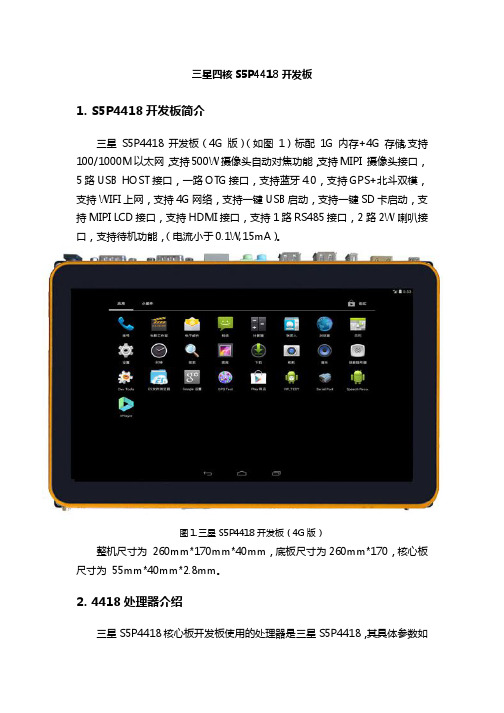
三星四核S5P4418开发板1.S5P4418开发板简介三星S5P4418开发板(4G版)(如图1)标配1G内存+4G存储,支持100/1000M以太网,支持500W摄像头自动对焦功能,支持MIPI 摄像头接口,5路USB HOST接口,一路OTG接口,支持蓝牙4.0,支持GPS+北斗双模,支持WIFI上网,支持4G网络,支持一键USB启动,支持一键SD卡启动,支持MIPI LCD接口,支持HDMI接口,支持1路RS485接口,2路2W喇叭接口,支持待机功能,(电流小于0.1W,15mA)。
图1.三星S5P4418开发板(4G版)整机尺寸为 260mm*170mm*40mm,底板尺寸为260mm*170,核心板尺寸为 55mm*40mm*2.8mm。
2.4418处理器介绍三星S5P4418核心板开发板使用的处理器是三星S5P4418,其具体参数如下。
型号:三星4418制程:28 nm 制程工艺指令集:ARMv7CPU架构:Cortex-A9CPU核心: 4CPU频率:1.4GHz支持MALI MP2 3D图形加速器、1M byte L2缓存视频解码能力:支持(H.264.MPEG4-ASP H.263 VC-1 MPEG-1/2 VP8 AVS RV8/9/10 RV8/9/10)1080P解码视频编码能力:支持(H.264 MPEG4 H.263)1080P编码3.S5P4418开发板硬件配置RP4418开发板(4G版)是一款高性能的四核Cortex-A9核心板,由深圳荣品电子设计、生产和发行销售。
它采用三星S5P4418处理器,运行主频可高达1.4GHz,S5P4418内部集成了Mali-400 MP高性能图形引擎,支持3D图形流畅运行,并可播放1080P全高清视频。
RP4418支持网卡、音频,1080P HDMI音视频同步输出等功能。
RP4418支持32位内存总线,支持1GB内存,支持动态电源管理,能够支持4GB、8GB、16GB、32GB INAND存储。
G3288开发板硬件手册说明书
G3288Development Board Hardware ManualShenzhen Graperain Technology Co.,Ltd.Copyright StatementCopyrights of this manual belong to Shenzhen Graperain Technology Co.,Ltd.and all rights are reserved.Any companies or individuals are not allowed to extract part or all of this manual,and violators will be prosecuted under law.Attention:The manuals of development platform on sell will be updated from time to time,please download the latest manual from website or contact our company sales representative,there would be no further notice.Release NoteTechnical supportAny questions about the manuals,you can call our landline or email us. Website:Landline:+8675523025312E-mail:**********************Sales and service networkShenzhen Graperain Technology Co.,Ltd.Website:Landline:+8675523025312E-mail:*******************Address:Building D,Huafeng Tech.&Innov.Park Baoan Wisdom Valley,Xixiang,Baoan Dist.Shenzhen,Guangdong.Post code518101.CatalogueChapter1.G3288Development Board Brief (6)1.1G3288development board brief (6)1.2Characteristics Parameter (6)1.3G3288Development Board Appearance (8)1.4G3288SOM Appearance (8)Chapter2.G3288Development Board Hardware Resource (9)2.1G3288Development Board Hardware Resource Brief (9)2.2G3288SOM PIN Definition (10)Chapter3.Hardware Design (13)Chapter4.Product Portfolio (14)4.1System on Module Series (14)4.2Development Board Series (14)4.3Single Board Computer(SBC)Series (14)Chapter1.G3288Development Board Brief1.1G3288development board briefG3288development board takes Rockchip RK3288chip,designed by Shenzhen Graperain Technology Co.,Ltd..G3288development board includes G3288system on module and carrier board.G3288system on module takes Rockchip RK3288CPU,its dominant frequency about1.8GHz, integrated Mali-T760MP4graphic processor,it supports OpenGL ES1.1/2.0/3.0,OpenVG1.1, OpenCL,Directx11,and could come out4k x2K H.264and10bits H265video hardware decoding.G3288carrier board PIN out all functions of this chip mostly.Its data transmission and scalability have been extremely good play.Such as4G onboard,OTG,USB2.0,gigabit ethernet,dual band WIFI,bluetooth,audio input/output,multiple sensors,RGB,LVDS,MIPI,HDMI ect display interfaces and communication interfaces,camera and TF card slot.G3288development board supports Android,Linux,and Ubuntu OS,and all of them source code is open,which will be convenient to clients to develop.G3288module could be used in commercial display advertisement machine,vending machine, teaching terminal,automatic identification,robot,security monitoring,financial POS,vehicle control terminal,VR and so on directly,which will save time on developing well.G3288Development Board Characteristics:●Size:186.5mm x115.6mm●Strong functions,rich interfaces,and applicable widely●Supports Android5.1,Linux,Ubuntu OS,open source code and accelerate R&D cycle●Product stability and reliability1.2Characteristics Parameter1.3G3288Development Board AppearanceG3288Development Board Front View1.4G3288SOM AppearanceMore information of G3288SOM,please reference G3288System on module introduction.Chapter2.G3288Development Board Hardware Resource 2.1G3288Development Board Hardware Resource BriefNote:More information of G3288system on module,please reference G3288system on module introduction.Chapter3.Hardware Design3.1Design ReferenceTaking GR3288SOM as hardware platform,you could refer to power design,USB design,HDMI design,LVDS design,MIPI design,Audio design,Internet(Network card,WIFI,Bluetooth)design, camera design,and so on.These are open to customers,can refer to our carrier board design.Chapter4.Product Portfolio4.1System on Module SeriesG4418SOM(Samsung S5P4418)G6818SOM(Samsung S5P6818)G3288SOM(Rockchip RK3288)M9SOM(Qualcomm8916)4.2Development Board SeriesG4418development board(Samsung S5P4418)G6818development board(Samsung S5P6818)G3288development board(Rockchip RK3288)M9development board(Qualcomm8916)4.3Single Board Computer(SBC)SeriesG4418single board computer(Samsung S5P4418)G6818single board computer(Samsung S5P6818)G3288single board computer(Rockchip RK3288)Instructions:More information of specifications and other products,please pay attention to website and contact us directly.。
NXP i.MX 8M EVK 开发板硬件用户指南说明书

© 2018 NXP B.V.i.MX 8M EVK Board Hardware User's Guide1.IntroductionThis document is the hardware User’s Guide for the i.MX 8M Evaluation Kit (EVK) based on the NXPSemiconductor’s i.MX 8M Applications Processor. This board is fully supported by NXP Semiconductor. This manual includes system setup and debugging, andprovides detailed information on the overall design and usage of the EVK board from a hardware system perspective.1.1. Board overviewThe EVK board is a platform designed to showcase the most commonly used features of the i.MX 8MApplications Processor in a small, low cost package. The i.MX 8M EVK board is a development board, which gives the developer the option of becoming familiar with the processor.Table 1 lists the features of the i.MX 8M EVK board.NXP Semiconductors User's GuideDocument Number: IMX8MDQLQEVKHUGRev. 1, 05/2018Contents1.Introduction ........................................................................ 11.1. Board overview ....................................................... 1 1.2. Board contents ........................................................ 2 1.3. Board revision history ............................................. 2 2.Specifications ..................................................................... 32.1. Processor ................................................................. 4 2.2. Boot mode operations and selections ...................... 5 2.3. Power tree ............................................................... 6 2.4. LPDDR4 DRAM memory ...................................... 8 2.5. SD card slot (J1601) ............................................... 8 2.6. eMMC memory (U601) .......................................... 9 2.7. Ethernet connector (J1201) ..................................... 9 2.8. USB connector (J901, J903) ................................... 9 2.9. Audio input/output (J1101) ..................................... 9 2.10. UART connector (J1701) ...................................... 10 2.11. JTAG connector (J401) ......................................... 10 2.12. Extension port (J1801) .......................................... 10 2.13. MIPI-CSI/MIPI-DSI connector (J1501, J1502, J1503) 102.14. User interface buttons ........................................... 12 2.15. WiFi/BT (U1301/J1401) ....................................... 12 2.16. User interface LED indicators ............................... 13 2.17. HDMI connector (J1001) ...................................... 133.PCB information .............................................................. 14 3.1. EVK design files ................................................... 144.EVK accessories .............................................................. 155.Revision history (16)IntroductionTable 1. Board featuresProcessor NXP Applications Processor MIMX8MQ6DVAJZAADRAM memory Micron 3 GB LPDDR4 MT53B768M32D4NQ-062 WT:B Mass storage Micron 16 GB eMMC5.0 MTFC16GAKAECN-2M WTMicron 32 MB QSPI NOR MT25QL256ABA1EW9MicroSD card connector SD3.0 supportedPower NXP PMIC PF4210 + Discrete DCDC/LDODisplay interface HDMI 2.0a ConnectorDSI interface (Mini-SAS connector)Ethernet 1 GB Ethernet with RJ45 connectorUSB x1 USB (2.0/3.0) Type-C connector x1 USB (2.0/3.0) host connectorAudio connectors 3.5 mm Stereo Headphone outputDebug connectors JTAG (10-PIN header) MicroUSB for UART debugCamera CSI interface (Mini-SAS connector)WiFi/Bluetooth x1 on board WiFi/BT module x1 M.2 slot (KEY-E type)Buttons ONOFF, RESETLED Indicators Power status, UARTExpansion Port FPC connector (SAI ports)PCB 3.937-inch x 3.937-inch (10 cm x 10 cm), 10-layer board1.2. Board contentsThe i.MX 8M EVK contains the following items:•i.MX 8M EVK board•USB Cable (x1 Standard USB TYPE-A to MicroUSB TYPE-B connector; x1 Standard USB TYPE-A to USB TYPE-C connector)•12V/5.0A Power Supply•Quick Start Guide1.3. Board revision history•Rev A0/A1•Rev B1/B2•Rev B3•Rev B4The board assembly version will be printed on a label, usually attached to the bottom side. The assembly version will be the letter designation following the schematic revision: 700-29615 REV _.2. SpecificationsThis section provides the detailed information about the electrical design and practical considerations that go into the EVK board. Figure 1 describes each block in the high-level block diagram of the EVK board.Figure 1. MCIMX8M-EVK block diagramFigure 2 shows the overview of the i.MX 8M EVK board.SpecificationsFigure 2. i.MX 8M EVK board overview2.1. ProcessorThe i.MX 8M processors represent NXP Semiconductor’s latest achievement in integrated multimedia-focused products offering high performance processing with a high degree of functional integration, targeted towards the growing market of connected devices. The i.MX 8M processor features NXP’s advanced implementation of the Quad Arm Cortex®-A53+ Arm Cortex-M4 core, which operates at speeds up to 1.5 GHz. i.MX 8M includes integrated power management module that reduces the complexity of external power supply and simplifies the power sequencing. Each processor provides a 32-bit LVDDR3L/DDR4/LPDDR4 memory interface and other interfaces for connecting peripherals, such as HDMI, LCD, WLAN, Bluetooth™, GPS and camera sensors.For more detailed information about the processor, please refer to the datasheet and reference manual on /i.MX8M.2.2. Boot mode operations and selectionsThe i.MX 8M Applications Processor can be the boot configuration selected on SW802 or by the boot configuration stored on internal eFUSE. Alternatively, the i.MX 8M can download a program image from a USB connection when configured in serial downloader mode. The method used to determine where the processor finds its boot information is from two dedicated BOOT MODE pins. Table 2 shows the values used in the two methods.Figure 3. Boot mode selection using SW802Table 2. Boot mode pin settingsBOOT_MODE1 BOOT_MODE 0 Boot source0 0 Boot from fuses0 1 Serial downloader1 0 Internal boot1 1 ReservedIt is important for the developer to remember that these two pins are tied to the BOOT modules, therefore, on i.MX 8M EVK board, use a dual-switch (SW802) to select the input voltage of these two pins, 0 or 3.3 V. If the developer wants to boot the program Image from the Fuses Mode, the position of the switch 1 and 2 must be set to OFF, it is the same principle to choose the Serial Downloader Module or Internal Boot Module to load bootable code into the processor.If the method of determining the bootable source code is selected to be from the hardware, then the developer must set the switch S802:MODE0 to OFF, MODE1 to ON, and the four i.MX 8M pins must be set on the EVK board as Table 3 and Figure 4.Table 3. Boot mode settingBOOT configuration SW801Boot from EMMC 0010Boot from SD2 1100SpecificationsFigure 4. Boot mode setting using SW801On the i.MX 8M EVK board, the default boot mode is from eMMC device. There is one SD connector on the board. The board will check the eMMC connector first and then the SD connector. If you put the boot card into SD connector, and set the boot configuration as “BOOT from SD2”, the board will boot from the SD by default.NOTEFor more information about the boot module, such as the meaning ofevery bit of the Boot Switch, please refer to i.MX 8M Reference Manualon /i.MX8M.2.3. Power treeThere is a +12 V external wall power supply that needs to be connected to the i.MX 8M EVK board at connector J902. The other powers from internal adapters, on the EVK board, use discrete device to power the system. Figure 5 shows the power tree.Figure 5. Power tree diagramIn Figure 5, the developer can get all the voltage supply rails used on the EVK board. When some modules are not working, the developer needs to test whether the voltage of this module is correct. Table 4 lists the power rails on the board.SpecificationsTable 4. Power railsi.MX8MQSRC TYPE Value SEQ PWR rail1 NVCC_SNVS DC/DC BUCK 3.32 VDD_SNVS LDO 0.93 VDD_SOC/VDDA_0P9 DC/DC BUCK 0.94 VDD_ARM DC/DC BUCK 0.9/1.04 VDD_GPU PMIC PF4210 0.9/1.04 VDD_VPU PMIC PF4210 0.9/1.04 VDD_DRAM PMIC PF4210 1.05 VDDA_1P8_xxx PMIC PF4210 1.85 VDDA_DRAM PMIC PF4210 1.86 NVCC_3V3 DC/DC BUCK 3.36 NVCC_1V8 PMIC PF4210 1.86 NVCC_DRAM PMIC PF4210 1.1/1.2/1.357 NVCC_SD2 LDO 1.8/3.38 1.8 V PHY PMIC PF4210 1.88 0.9 V PHY PMIC PF4210 0.98 3.3 V PHY PMIC PF4210 3.3NOTEIf an alternate power supply is used (not the original power supply), itshould be no more than 20 V; otherwise the board will not work.2.4. LPDDR4 DRAM memoryThe i.MX 8M EVK board has one 768 Meg × 32 (4 channels × 16 I/O) LPDDR4 SDRAM chip(MT53B768M32D4NQ-062 WT:B) for a total of 3 GB RAM memory.In the physical layout, the LPDDR4 chip is placed on the TOP side, the data traces are not necessarily connected to the LPDDR4 chips in sequential order, but for ease of routing, are connected as best determined by the layout and other critical traces.The DRAM_VREF can be created by a simple voltage divider using 1.5 K Ohm 1% resistors and 0.1 µF capacitors for stability. The relatively smaller-value resistors provide enough current to maintain a steady mid‐point voltage. The calibration resistors used by the LPDDR4 chips and processor are 240 Ohm 1% resistors.2.5. SD card slot (J1601)There is one MicroSD card connectors (J1601) on the i.MX 8M EVK board. J1601 on the i.MX 8M EVK board is the TF slot for SD2 interface. By default, this MicroSD connector supports one 4-bitSD3.0 card or MMC card.2.6. eMMC memory (U601)The eMMC interface is connected to uSDHC1 of i.MX 8M. It can support eMMC 5.0, eMMC and hinge type. MicroSD socket are co-layout, and the eMMC device is populated by default on the EVK board. To boot from eMMC, you need to change the Boot-mode switch (SW801) settings as shown in Table 3.2.7. Ethernet connector (J1201)There is one gigabit Ethernet module on the i.MX 8M processor. The developer can use the ENET connector to send/receive the ENET signals. The Ethernet subsystem of the i.MX 8M EVK board is provided by the Qualcomm AR8031 Ethernet Transceiver (U1201). The Ethernet Transceiver (or PHY) receives standard RGMII Ethernet signals from the MAC-NET core of the i.MX 8M Applications Processor. The processor takes care of all Ethernet protocols at the MAC layer and above. The PHY is only responsible for the Link Layer formatting. The PHY receives the clock signal from the ENET_TXC pin of i.MX 8M processor.2.8. USB connector (J901, J903)The i.MX 8M Applications Processors contain two USB 2.0/3.0 OTG controllers, with two integrated USB PHY. On the EVK board, one is used for USB host port and the other for the USB TYPE-C port.2.9. Audio input/output (J1101)The main Audio DAC used on the EVK board is CIRRUS LOGIC Low Power, high quality Stereo DAC, WM8524. The digital interface between i.MX 8M and WM8524 includes three signals:SYNC_CLK, BCLK, and DACDAT. The i.MX 8M also provides the MCLK to WM8960.i.MX 8M EVK includes one headphone interface (J1101). J1101 is a 3.5 mm 4-pole (or TRRS) phone jack.CAUTIONThe Stereo audio jack is designed to be connected with active speaker. Ifyou want to connect it with a headphone, please make sure that theheadphone has volume control functionality and set the headphone’svolume properly before wearing it. Please do not plug in the non-volume-control headphone directly. The audio output volume may be too loud fornon-volume-control headphone and may harm your hearing.Specifications2.10. UART connector (J1701)The i.MX 8M Applications Processor has four independent UART Ports (UART1 – UART4). Usually the developer can use a DB9 connector and a level shifter such as MAX3232 to complete the UART debug circuit. Nowadays, many computers may not have a RS-232 DB9 connector, so on the EVK board, SILICON LABS’s CP2105, there is a USB to Serial UART IC to convert the UART signal to the USB signal. Note that you need to make sure the CP2105 VCP Driver has been installed on your computer for proper operation. If not, you may download it from SILICON LABS’ website and install: https:///products/development-tools/software/usb-to-uart-bridge-vcp-driversOn the EVK board, UART1_TXD & UART1_RXD are used to output serial debugging information for A53-core. UART2_TXD & UART2_RXD are used to output serial debugging information for M4-core. No RTS or CTS signals are sent from the Processor to the Debug connector as these signals are ignored by most applications. The required terminal settings to receive debug information during the boot cycle are as shown in Table 5.Table 5. Terminal setting parametersData Rate 115,200 BaudData bits 8Parity NoneStop bits 12.11. JTAG connector (J401)The i.MX 8M Applications Processor accepts five JATG signals from an attached debugging device on dedicated pins. A sixth pin on the processor accepts a board HW configuration input, specific to the EVK board only. The five JTAG signals used by the processor are:•JTAG_TCK TAP Clock•JTAG_TMS TAP Machine State•JTAG_TDI TAP Data In•JTAG_TDO TAP Data Out•JTAG_nTRST TAP Reset Request (Active Low)2.12. Extension port (J1801)One Expansion port (J1801) is provided on the EVK board to generate audio card connector, and the developer can use the processor to perform audio features development.2.13. MIPI-CSI/MIPI-DSI connector (J1501, J1502, J1503)The i.MX 8M processor supports dual MIPI-CSI and single MIPI-DSI. The connectors are designed to support camera and LCD. The connectors are as shown in Figure 6.Figure 6. MIPI-DSI/CSI connectorNOTEThe dual MIPI-CSI connector on Rev B3 EVK board shares the same I2C bus, if you want to develop dual-camera applications using two identical camera modules (with the same I2C address), an SW patch may be required (e.g., power on camera0 while keep camera1 powered off, then change camera0 I2C address and power on camera1). Alternatively, you can use two camera modules with different I2C address. Rev B4 EVK improving by assigning a different I2C bus to each MIPI-CSI connector, therefore not requiring a SW patch.Specifications2.14. User interface buttonsThere are two user interface buttons on the EVK board.2.14.1. Power button (SW1701)The chip supports the use of a button input signal to request main SoC power state changes (i.e. ON or OFF) from the PMU.ON/OFF can be configured as debounce, OFF-to-ON time, and max timeout. The debounce and OFF-to-ON time can be configured as 0, 50, 100 and 500 ms. Debounce is used to generate the power-off interrupt. In the ON state, if ON/OFF button is held longer than the debounce time, the power-off interrupt is generated. OFF-to-ON time supports the time it takes to request power-on after a button has been held longer than the configured time. In the OFF state, if ON/OFF button is held longer than the OFF-to-ON time, the state will transit from OFF to ON. Max timeout can be configured as 5 s, 10 s, 15 s and disable. Max timeout can also be the time for requesting power down after ON/OFF button has been held for the defined time.2.14.2. Reset button (SW1702)In the ON state, holding the RESET button (SW1702) will force to reset the power rails except the VDD_SNVS on the i.MX 8M EVK board. The i.MX 8M applications processor will be immediately turned off and reinitiate a boot cycle from the OFF state.2.15. WiFi/BT (U1301/J1401)The MCIMX8M EVK board has two ways to support WiFi/BT function:1.Chip on board WiFi: LBEE5U91CQ-TEMP;2.M.2 WiFi/BT card.Both ways share the same UART interface for BT function, so the BT function cannot be used at the same time. For WiFi, there are two standalone PCIe interfaces for this purpose, and WiFi function can be used at the same time.2.16. User interface LED indicatorsThere are two LED indicators on the board. These LEDs have the following functions: •Main Power Supply (D1601)—Green – CPU is running on OD mode.—Red – WALL_12V_DC_JACK is provided and SW701 is powered on.—OFF – The board is powered off.•UART (D1702/D1703)—Green light flashing – The UART data transmitted to PC.—Orange light flashing – The UART data received from PC.2.17. HDMI connector (J1001)The i.MX 8M EVK board has a Type-A HDMI connector that can playback 4K video.EVK accessories3. PCB informationThe overall dimensions of the i.MX 8M EVK board PCB are shown in Figure 2. The EVK board is made with standard 10-layer technology. The material used is FR-4, and the PCB stack-up information is shown in Table 6.Table 6. Board stack up informationLayer Description Coppoer (Oz.) Dielectric thickness (mil)1 Signal 0.333Dielectric TU768P: 2.741 mil2 GND 1Dielectric TU768P: 3.94 mil3 Power 1Dielectric TU768P: 4.409 mil4 Signal 1Dielectric TU768P: 3.94 mil5 GND 1 3.0Dielectric TU768P: 4.491 mil6 Signal 1Dielectric TU768P: 3.94 mil7 GND 1Dielectric TU768P: 4.465 mil8 Signal 1Dielectric TU768P: 3.94 mil9 GND 1Dielectric TU768P: 2.743 mil10 Signal 0.3333.1. EVK design filesYou can download the schematics, layout file, gerber files, and BOM from /i.MX8M.NOTEThe EVK thermal design was performed for a typical use case. Ensureyour thermal design is based on your specific use case.4. EVK accessoriesFor developers’ wishing to implement display or camera functionality through MIPI-DSI/CSI interface, NXP provides three optional accessories that can be directly attached to the mini-SAS connector on EVK board. The developer can purchase these accessories from NXP website.Table 7 shows the link to each accessory, in which you can find the user guide and design files of the accessory.Table 7. Links to accessories for the i.MX8M EVKAccessory Description LinkIMX-MIPI-HDMI Converts MIPI-DSI signal to HDMI signal /part/IMX-MIPI-HDMIMX8-DSI-OLED1 MIPI-DSI interface OLED display kit with touch screen /part/MX8-DSI-OLED1 MINISASTOCSI MIPI-CSI interface camera kit based on OmniVision/part/MINISASTOCSI chipset OV5640Revision history5.Revision historyTable 8. Revision historyRevision number Date Substantive changes0 01/2018 Initial release.1 05/2018 •Removed DQLQ suffix in the whole text.•Updated Note in 3.1 EVK design files.•Updated Table 4.•Updated Figure 2.•Added Caution to 2.9 Audio input/output (J1101).•Added 4 EVK accessories.Document Number: IMX8MDQLQEVKHUGRev. 1 05/2018How to Reach Us: Home Page: / Web Support:/supportInformation in this document is provided solely to enable system and softwareimplementers to use NXP products. There are no express or implied copyright licenses granted hereunder to design or fabricate any integrated circuits based on the information in this document. NXP reserves the right to make changes without further notice to any products herein.NXP makes no warranty, representation, or guarantee regarding the suitability of its products for any particular purpose, nor does NXP assume any liability arising out of the application or use of any product or circuit, and specifically disclaims any and all liability, including without limitation consequential or incidental damages. “Typical” parameters that may be provided in NXP data sheets and/or specifications can and do vary in different applications, and actual performance may vary over time. All operating parameters, including “typicals,” must be validated for each customer application by customer’s technical experts. NXP does not convey any license under its patent rights nor the rights of others. NXP sells products pursuant to standard terms and conditions of sale, which can be found at the following address: /SalesTermsandConditions .NXP, the NXP logo, NXP SECURE CONNECTIONS FOR A SMARTER WORLD, Freescale, the Freescale logo are the trademarks of NXP B.V. All other product or service names are the property of their respective owners.Arm, the Arm logo, and Cortex are registered trademarks of Arm Limited (or its subsidiaries) in the EU and/or elsewhere. All rights reserved. © 2018 NXP B.V.Mouser ElectronicsAuthorized DistributorClick to View Pricing, Inventory, Delivery & Lifecycle Information:N XP:MCIMX8M-EVK。
G4418 硬件手册
G4418硬件手册深圳葡萄雨技术有限公司版权声明本手册版权归属深圳市葡萄雨技术有限公司所有,并保留一切权力。
非经葡萄雨技术有限公司同意(书面形式),任何单位及个人不得擅自摘录本手册部分或全部,违者我们将追究其法律责任。
如果您对文档有所疑问,您可以拨打技术支持电话或E-mail联系。
网址:/联系电话:0755-********目录版权声明..........................................................................................错误!未定义书签。
第1章G4418开发板简介 (8)1.1产品简介 (10)1.2功能特性 (11)1.3搭载系统简介 (12)1.3.1Android4.4系统 (12)1.3.2Linux QT系统 (13)1.3.3Ubuntu系统 (13)第2章硬件资源 (14)2.1硬件接口描述 (14)2.2开发板启动指引 (16)2.3接口定义 (17)2.3.1核心板引脚定义1 (17)2.3.2核心板引脚定义2 (18)2.3.3核心板引脚定义3 (18)2.3.4核心板引脚定义4 (19)2.3.5核心板引脚定义5 (20)2.3.6J18(SPI扩展口) (20)2.3.7LCD1(LCD&VGA扩展口) (20)2.3.8J14(LVDS显示扩展口) (22)2.3.9J12(MIPI显示扩展口) (22)2.3.10U451(DVP camera接口) (23)2.3.11J15(MIPI camera接口) (24)2.3.12J11(UART1,COM1) (25)2.3.13J17(UART2,COM3) (25)2.4硬件接口 (25)2.4.1电源开关及插座 (25)2.4.2调试串口 (25)2.4.3HDMI接口 (26)2.4.4DVP camera接口 (26)2.4.5MIPI camera接口 (27)2.4.6以太网接口 (27)2.4.7耳机接口 (27)2.4.8喇叭接口 (28)2.4.9录音接口 (28)2.4.10TF卡槽 (28)2.4.11独立按键 (28)2.4.12调试LED灯 (29)2.4.13电源指示灯 (29)2.4.14USB OTG接口 (30)2.4.15USB HOST接口 (30)2.4.16开机按钮 (30)2.4.17复位按钮 (30)2.4.18LCD接口 (31)2.4.19后备电池 (31)2.4.20精准可调电位器 (31)2.4.21蜂鸣器 (31)2.4.22红外一体接收头 (32)2.4.23LVDS接口 (32)2.4.24MIPI接口 (32)2.4.25电池接口 (33)2.4.26PCIE3G/4G接口 (33)2.4.27SPI接口 (33)2.5底板尺寸图 (34)第3章配置清单 (35)3.1标配硬件清单 (35)3.2选配硬件清单 (35)3.3网盘资料清单 (35)第4章产品线介绍 (36)4.1核心板系列 (36)4.2开发板系列 (36)4.3卡片电脑系列 (36)第1章G4418开发板简介本文档讲述G4418开发平台的硬件资源,电路原理,支持的接口,等。
迅为4418开发板7-24小时无故障运行
迅为4418开发板7*24小时无故障运行
核心板参数
核心板类型板对板邮票孔特点拆装便利,扩展性好适合高震惊场合尺寸50mm*60mm层数6层PCB沉金设计8层PCB沉金设计衔接器高度核心板衔接器组合高度1.5mm04418 CPU -A9 四核 S5P4418处理器
1.4GHz6818 CPUARM Cortex-A53 八核 S5P6818处理器 1.4GHz内存1GB
DDR3(2GB可选)1GB DDR3存储16GB EMMC16GB EMMCAXP228(官方推举),支持动态调频,超低功耗工作直流5V供电系统支持4.4/5.1.1/7.1系统、3.4.39、QT2.2/4.7/5.7、12.04运行温度0℃-70℃0℃-70℃引角扩展四组衔接器共320个PIN脚208个PIN脚扩展参数:24位RGB 888,可按照屏幕要求取舍;
LVDS:4通道、可配置;
:v1.4;
MIPI:DSI和CSI各一个,支持LCD和CAMARA;DVP:可支持DVP格式并口摄像头;
SDIO:3个(1路被占用);
_HOST:1个,底板扩展3个;
USB_OTG:1个,底板作为DEV用;
USB_HSIC:1个;
UART:6路;
I2C:3路,可用于等;
SPDIF:1路;
GPIO:多数已引出;
SPI:3路;
以太网:1路自适应10/100/1000;
:3路,可用于背光控制;
锂电池充放电:引出,可挺直用法(带电量计);:7路模拟输入;
第1页共3页。
4418开发板介绍
UT4418开发板介绍友坚恒天科技专注于三星平台产品的研发,是三星在中国最具实力的方案公司。
公司主打的三星平板电脑方案销量,连续多年稳居第一。
公司定位于中高端产品的研发,具有多年的嵌入式产品研发经验;基于三星A15-Exynos5260/5410/5250、S5P4418、A9-Exynos4412、A8-S5PV210、ARM11-S3C6410、ARM9-S3C2416等处理器,开发了系列化的产品,为客户提供了全面的产品选择及专业化的量身定制MID解决方案。
友坚恒天科技服务于国内外平板电脑品牌商,并为行业客户提供一站式的解决方案;在为客户打造最具竞争力优势的产品的同时,也实现了自身的价值。
UT4418处理器是三星2014年推出的4核处理器,使用Cotex-A9四核心,整体性能比Cotex-A8核心高出50%,提供6.4GB/s内存带宽,支持1080P的全高清视频输出,以及3D 图形显示,支持LCD显示1080P高清电视输出等,完全是Exynos4412的升级版芯片,性能远远超过Exynos4412,并且基本兼容Exynos4412。
UT4418开发板为消费类电子、智能终端、MID、无线通讯、移动导航、医疗设备、工业控制等行业产品的应用开发而设计,供广大企业用户进行产品前期软硬件性能评估验证、设计参考用;也是高校、培训机构、嵌入式爱好者学习研究的最佳工具。
UT4418开发板标准板外观图:友坚UT4418开发板UT4418开发板升级板外观图:友坚UT4418开发板UT4418开发板采用一体化的设计,提高了电路整体的稳定性。
UT4418开发板标配了4G iNAND(SDIN5C1-4G),内存配置了1G DDR3(H5TQ4G63AFR-PBC)并配备有三星电源管理芯片——NXE2000;PCB布局布线充分考虑电气要求,具有极佳的性能和抗干扰特性,敬请留意:使系统稳定工作于各种环境之下。
强大的功能,丰富的外设接口,是用户熟悉UT4418开发板软硬件环境的最佳选择。
三星四核S5P4418开发板RP4418介绍新

三星四核S5P4418开发板RP4418介绍四核S5P4418处理器是三星2014年推出的四核处理器,使用Cotex-A9四核心,整体性能比Cotex-A8核心高出50%,提供6.4GB/s 内存带宽,支持1080P 的全高清视频输出,以及3D 图形显示,支持LCD 显示1080P 高清电视输出等,完全是Exynos4412的升级版芯片。
RP4418开发板为消费类电子、智能终端、MID、无线通讯、移动导航、医疗设备、工业控制等行业产品的应用开发而设计,供广大企业用户进行产品前期软硬件性能评估验证、设计参考用;也是高校、培训机构、嵌入式爱好者学习研究的最佳工具。
RP4418开发板由深圳荣品电子研发,采用一体化的设计,提高了电路整体的稳定性。
搭配Android5.1系统,标配1GB DDR3内存,16GB EMMC 存储并配备有三星电源管理芯片AXP228 ;PCB 布局布线充分考虑电气要求,具有极佳的性能和抗干扰特性,使系统稳定工作于各种环境之下。
强大的功能,丰富的外设接口,是用户熟悉RP4418开发板软硬件环境的最佳选择。
RP4418核心板硬件参数 引脚编号引脚名称 输入/输出说明1 VSYS_IN IN 电源输入 3.4V 至5.5V2 VSYS_IN IN3 GND IN-OUT 接地4 GND IN-OUT5 GPIOC24 IN-OUT GPIO 控制口6 GPIOC17 IN-OUT GPIO 控制口 7 OUT-3V3-1A OUT 可外供电 3.3V 负载1A8 VDD_RTC IN RTC 时钟保存电源输入1.8V 至3V9 LCD_CLK OUT LCD 时钟10 R0 OUT LCD 数据通道(可复用GPIO )11 R1 OUT 12 R2 OUT 13 R3 OUT 14R4OUT15 R5 OUT16 R6 OUT17 R7 OUT18 G0 OUT19 G1 OUT20 G2 OUT21 G3 OUT22 G4 OUT23 G5 OUT24 G6 OUT25 G7 OUT26 B0 OUT27 B1 OUT28 B2 OUT29 B3 OUT30 B4 OUT31 B5 OUT32 B6 OUT33 B7 OUT34 HSYNC OUT LCD数据行(可复用GPIO)35 VSYNC OUT LCD数据场(可复用GPIO)36 DE OUT LCD数据模式(可复用GPIO)37 GPIOC8 IN-OUT GPIO控制口38 PWM0 OUT PMW定时器39 SDA1 IN-OUT I2C通道1 数据信号40 SCL1 OUT I2C通道1 时钟信号41 GPIOB26 IN-OUT GPIO控制口42 GPIOC14 IN-OUT GPIO控制口43 LVDS_CLKP OUT LVDS 时钟正44 LVDS_CLKN OUT LVDS 时钟负45 LVDS_Y0P OUT LVDS 数据通道0正46 LVDS_Y0N OUT LVDS 数据通道0负47 LVDS_Y1P OUT LVDS 数据通道1正48 LVDS_Y1N OUT LVDS 数据通道1负49 LVDS_Y2P OUT LVDS 数据通道2正50 LVDS_Y2N OUT LVDS 数据通道2负51 LVDS_Y3P OUT LVDS 数据通道3正52 LVDS_Y3N OUT LVDS 数据通道3负53 LCD_MIPI_CLKP OUT MIPI 时钟正54 LCD_MIPI_CLKN OUT MIPI 时钟负55 LCD_MIPI_DP0 OUT MIPI 数据通道0正56 LCD_MIPI_DN0 OUT MIPI 数据通道0负57 LCD_MIPI_DP1 OUT MIPI 数据通道1正58 LCD_MIPI_DN1 OUT MIPI 数据通道1负59 LCD_MIPI_DP2 OUT MIPI 数据通道2正60 LCD_MIPI_DN2 OUT MIPI 数据通道2负61 LCD_MIPI_DP3 OUT MIPI 数据通道3正62 LCD_MIPI_DN3 OUT MIPI 数据通道3负63 SD0_CD IN TF卡检测脚64 SD0_D1 IN-OUT SD通道0数据165 SD0_D0 IN-OUT SD通道0数据066 SD0_CLK OUT SD通道0时钟67 SD0_CMD IN-OUT SD通道0使能68 SD0_D3 IN-OUT SD通道0数据369 SD0_D2 IN-OUT SD通道0数据270 SD1_D1 IN-OUT SD通道1数据171 SD1_D0 IN-OUT SD通道1数据072 SD1_CLK OUT SD通道1时钟73 SD1_CMD IN-OUT SD通道1使能74 SD1_D3 IN-OUT SD通道1数据375 SD1_D2 IN-OUT SD通道1数据276 TXD1 OUT TTL串口通道1发送77 RXD1 IN TTL串口通道1接收78 RTS1 OUT TTL串口通道1发送数据请求79 CTS1 OUT TTL串口通道1清除数据80 SDA2 IN-OUT I2C通道2 数据信号81 SCL2 OUT I2C通道2 时钟信号82 GPIOB25 IN-OUT GPIO控制口83 GPIO3 IN-OUT GPIO控制口84 VDD33_WIFI OUT WIFI电源3.3V输出85 ADC0 IN 模拟ADC0通道支持0~1.8V86 TXD2 OUT TTL串口通道2发送87 RXD2 IN TTL串口通道2接收88 TXD3 OUT TTL串口通道3发送89 RXD3 IN TTL串口通道3接收90 USB_BOOT IN USB启动方式91 SD_BOOT IN SD卡启动方式92 KEY_RST IN 复位键93 KEY_PWR IN 开机键94 GPIOB30 IN-OUT GPIO控制口95 GPIOB31 IN-OUT GPIO控制口96 GPIO5 IN-OUT GPIO控制口97 SPICLK0 OUT SPI0通道时钟(可复用GPIO)98 SPICS0 OUT SPI0片选(可复用GPIO)99 SPITX0 OUT SPI0发送(可复用GPIO)100 SPIRX0 IN SPI0发送(可复用GPIO)101 SPICLK2 OUT SPI2通道时钟(可复用GPIO)102 SPICS2 OUT SPI2片选(可复用GPIO)103 SPITX2 OUT SPI2发送(可复用GPIO)104 SPIRX2 IN SPI2接收(可复用GPIO)105 MIPI_DN0 IN 摄像头MIPI0数据负106 MIPI_DP0 IN 摄像头MIPI0数据正107 MIPI_DN1 IN 摄像头MIPI1数据负108 MIPI_DP1 IN 摄像头MIPI1数据正109 MIPI_CKN IN 摄像头MIPI0时钟负110 MIPI_CKP IN 摄像头MIPI0时钟正111 MIPI_DN2 IN 摄像头MIPI2数据负112 MIPI_DP2 IN 摄像头MIPI2数据正113 MIPI_DN3 IN 摄像头MIPI3数据负114 MIPI_DP3 IN 摄像头MIPI3数据正115 CAM0_D2 IN YUV摄像头数据2(可复用GPIO)116 CAM0_D1 IN YUV摄像头数据1(可复用GPIO)117 CAM0_D3 IN YUV摄像头数据3(可复用GPIO)118 CAM0_D0 IN YUV摄像头数据0(可复用GPIO)119 CAM0_D4 IN YUV摄像头数据4(可复用GPIO)120 CAM0_PCLK IN YUV摄像头时钟输入(可复用GPIO)121 CAM0_D5 IN YUV摄像头数据5(可复用GPIO)122 CAM0_D6 IN YUV摄像头数据6(可复用GPIO)123 CAM_MCLK OUT YUV摄像头时钟输出(可复用GPIO)124 CAM0_D7 IN YUV摄像头数据7(可复用GPIO)125 CAM_2V8 OUT 摄像头电源2.8V126 CAM_1V8 OUT 摄像头电源1.8V127 GND IN-OUT 接地128 CAM0_HS IN YUV摄像头行信号129 GPIOA28 IN-OUT GPIO控制口130 GPIOB24 IN-OUT GPIO控制口131 CAM0_VS IN YUV摄像头场信号132 GPIOB9 IN-OUT GPIO控制口133 OTG_PWR OUT VBUS 5V 使能脚134 VBUS OUT VBUS 电源135 OTG_DN IN-OUT USB数据负136 OTG_DP IN-OUT USB数据正137 ID IN 主从模式检测138 HDMI_HPD IN HDMI检测139 HDMI_CEC IN HDMI检测140 HDMI_TXCN OUT HDMI时钟负141 HDMI_TXCP OUT HDMI 时钟正 142 HDMI_TX0N OUT HDMI 数据0负 143 HDMI_TX0P OUT HDMI 数据0正 144 HDMI_TX1N OUT HDMI 数据1负 145 HDMI_TX1P OUT HDMI 数据1正 146 HDMI_TX2N OUT HDMI 数据2负 147 HDMI_TX2POUT HDMI 数据2正148 GND IN-OUT 接地 149 HOST_DP IN-OUT USB 数据正 150 HOST_DN IN-OUT USB 数据负 151 GPIO8 IN-OUT GPIO 控制口 152 SDA0 IN-OUT I2C 通道0 数据信号 153 SCL0 OUT I2C 通道0 时钟信号154 I2S_IN IN I2S 数据输入 155 GPIOC4 IN-OUT GPIO 控制口 156 I2S_OUT OUT I2S 数据输出 157 I2S_LRCK IN I2S 时钟输入 158 I2S_BCK IN I2S 时钟输入 159 I2S_MCLK OUT I2S 主时钟输出 160 GPIOB27 IN-OUT GPIO 控制口161 GND IN-OUT 接地162 GMAC_MDIO IN-OUT 以太网PHY 接口(可复用GPIO )163 GMAC_MDIO IN-OUT 164 PHY_NRST IN-OUT 165 GMAC_TXEN IN-OUT 166 GMAC_TXD3 IN-OUT 167 GMAC_TXD2 IN-OUT 168 GMAC_TXD1 IN-OUT 169 GMAC_TXD0 IN-OUT 170 GMAC_TXCLK IN-OUT 171 PHY_INT IN 172 GMAC_RXCLK IN-OUT 173 GMAC_RXD3 IN-OUT 174 GMAC_RXD2 IN-OUT 175 GMAC_RXD1 IN-OUT 176 GMAC_RXD0 IN-OUT 177 GMAC_RXDVIN-OUT 178 GND IN-OUT 接地179 TXD0 OUT TTL 串口通道0发送 180 RXD0 IN TTL 串口通道0接收 181 TXD4 OUT TTL 串口通道4发送 182RXD4INTTL 串口通道4接收RP4418开发板主板RP4418开发板规格参数 屏幕 屏幕尺寸 10.1寸屏A (可选其他屏) 分辨率1024*600核心板参数尺寸40*55mm高度 2.8mm工艺6层板,通孔工艺,高强度半空工艺CPU 三星S5P4418 28nm 间距0.65 尺寸17*17mm 513 FCFBGA封装Cortex-A9 四核32KB*4 I/D 缓存1MB 二级缓存CPU主频1400MHz DDR3最高主频933MHz内存1GB 32位数据总线DDR3主频最高933MHz(批量可定制2GB) 存储16GB EMMC4.5(批量可定制4/8GB)PMU AXP228电源变频管理,待机电流小于15mAGPU Mali-400 MP引角扩展引出脚多达182PIN,满足用户各类实用扩展需求温度范围-20℃到70℃工作电压5V(推荐使用标配5V/3A电源线)系统支持Android5.1、Android4.4、Ubuntu12.04、Linux+QT4.8底板参数尺寸260*170*40mmPW 选配排针式5V电源输入LVDS LCD 支持LVDS 最高分辩率1280x800 接口附带电阻电容触摸屏信号MIPI LCD 支持mipi DSI 最高分辩率1920x1200 接口附带电阻电容触摸屏信号(暂不支持)4G ANT 4G 天线接口4G Model Mini pcie 接口,支持移动,联通,电信SIM Card 手机SIM卡(大卡)TF Card TF卡接口,最大支持64GB存储WiFi蓝牙GPS模块三合一模块GPS+WIFI+BT4.0,7路GPIO口,3路TTL串口,1路HOST,1路I2CUSB boot USB启动烧录按键SD boot SD卡启动烧录按键RV1 ADC0通道,可调电位器Power 开机键,长按3S开机,长按3S 点击系统关机Reset 系统复位键Gpio 2路SPI通道,3路外部中断口,5V电源输出,3.3V电源输出MIPI camera 500W MIPI数据摄像头接口YUV camera 500W BT656格式摄像头接口RS485 RS485 总线接口SPK 8欧1W classD类2 路喇叭输出USB OTG USB OTG 2.0协议HDMI HDMI 1.4a 最大分辩1920x1080UBS host 5路USB HOST接口2.0协议Phone 3.5立体声耳机输入,支持插拔检测MIC 支持-42dB 高灵敏度麦克风输入Ethernet 10M/100M/1000M自适应主控集成以太网UART4 RS232串口4通道UART0 RS232调试串口0 通道DC-5V 5V/3A 电源输入RGB LCD 24位色RGB通道,最大分辩率2048x1280 或可扩展32路GPIO口VDD_RTC 3V 200mA 电池, 时间可保存至5年以上User key 6路自定义按键G-sensor 三轴重力传感器BM250。
三星S5P4418核心板开发板简介

三星S5P4418核心板开发板介绍1.4418核心板简介RP4418C核心板是采用三星ARM Cortex-A9四核架构,主芯片完整型号三星4418,由荣品电子科技设计开发的一款多功能核心板(如图1)。
运行主频最可高达1.4GHz,三星4418支持MALI MP2 3D图形加速器、1M byte L2缓存,视频解码能力:支持(H.264.MPEG4-ASP H.263 VC-1 MPEG-1/2 VP8 AVS RV8/9/10 RV8/9/10)1080P解码;视频编码能力:支持(H.264 MPEG4 H.263)1080P编码。
尺寸为 55mmx 40mm,脚位数 182Pin。
核心板标配1GB DDR2内存和4GB高性能eMMC4.5闪存(另可选配等容量),搭载Android4.4操作系统。
图1.三星S5P4418核心板2.处理器介绍三星S5P4418核心板开发板使用的处理器是三星S5P4418,其具体参数如下。
型号:三星4418制程:28 nm 制程工艺指令集:ARMv7CPU架构:Cortex-A9CPU核心: 4CPU频率:1.4GHz支持MALI MP2 3D图形加速器、1M byte L2缓存视频解码能力:支持(H.264.MPEG4-ASP H.263 VC-1 MPEG-1/2 VP8 AVS RV8/9/10 RV8/9/10)1080P解码视频编码能力:支持(H.264 MPEG4 H.263)1080P编码3.参数配置3.1 CPU外理器- Samsung 4418,Quad Cortex-A9- 运行主频1400MHz- GPU Mali-400 MP3.2 内存 DDR3- 1GB DDR3 (标配)- 32bit 数据总线3.3 存储 EMMC- 4GB (标配)- 4GB/16GB(选配)3.4 其它参数- 6层板,沉金工艺- 核心板尺寸55mm* 40mm* 2.5mm- 高强度半孔板工艺- 工作环境温度 -20~80摄氏度3.5 软件资源- Android 4.44.硬件部分大部分的核心板开发板产品都会有硬件结构图和引脚定义,RP4412核心板的结构图如图2,其引脚定义如图3,4,5,6。
4418开发板 三星A9开发平台
4418开发板三星A9开发平台iTOP-4418开发板预装Android4.4.4 系统,支持9.7 寸、7 寸、4.3 寸屏幕,操作流畅;4418完美兼容八核6818处理器,独家提供1GB和2GB内存版本,核心板支持电池管理,充放电电路与电量计,板载千兆以太网,3G,GPS,WIFI蓝牙,陀螺仪等模块。
Android4.4.4 系统操作应用实例。
部分功能需要相应配套硬件,烧写对应的镜像才能测试。
系统基本功能1. 开机开发板接通电源,并按下电源开关,系统即启动,在启动过程中,系统会显示下图中的开机画面,它们分别是Android系统启动时的Logo 画面:最后会显示如下解锁画面:解锁后进入下图所示界面,点击正下方圆圈按钮可以进入Android界面。
2.音量调节同样在系统‘设置’里进行操作,如下图所示:用户也可以通过开发板上的按键,Vol+和Vol-来调节音量。
如下图所示:3.亮度调节操作方法和您使用手机或者平板的方法基本一样,通过按键来控制,如上图。
对于‘暴风影音’等视频播放软件,可以通过在屏幕上滑动等方式调节亮度;除此之外,在Android中可以通过系统‘设置’来调节亮度,如下图所示:B和OTG功能连接U 盘当插入U盘以后(底板上3 个USB 接口都可以插入U 盘),如下图所示:使用ES 文件浏览器就可以找到对应的U 盘。
如下图所示。
鼠标及键盘USB2.0 鼠标和键盘都可以支持。
在USB HOST 接口连接鼠标或键盘,Android系统会自动识别,对于没有购买触摸屏,使用HDMI显示器的用户,这是个很好的选择。
将开发板当做平板与PC 相连将开发板的OTG接口和PC 机的USB 接口相连,在Android桌面的右下部分状态栏将出现相应提示,如下图所示:5.网络设置和连接WIFI 连接默认支持。
WIFI功能需要在系统‘设置’里打开,连接方法和智能手机一模一样,如下图所示,已经连接。
有线网(RJ45)默认支持。
MikroElektronika PIC18FK 4K 系列开发板说明书
Compact development system rich with on-board peripherals for all-round multimedia development on PIC18F67K40 device.for PIC18FKmikromediaNebojsa MaticGeneral ManagerThe PIC®, dsPIC®, PIC24®, PIC32® and Windows® logos and product names are trademarks of Microchip Technology® and Microsoft® in the U.S.A. and other countries.Introduction to mikromedia for PIC18FK4 Package Contains 5 Key Features 6 System Specification 7 1. Power supply 8Battery power supply 8 USB power supply 8 2. PIC18F67K40 microcontroller 9Key microcontroller features 9 3. Programming the microcontroller 10 Programming with mikroBootloader 11 step 1 – Connecting mikromedia 11 step 2 – Browsing for .HEX file 12 step 3 – Selecting .HEX file 12 step 4 – Uploading .HEX file 13 step 5 – Finish upload 14 Programing with mikroProg programmer15 mikroProg Suite for PIC® Software 16 Programing with ICD2® or ICD3® programmer 174. Reset Button 185. microSD Card Slot 196. Crystal oscillator 207. Audio Module 218. Touch Screen 229. Accelerometer 2310. USB connection 2411. Flash Memory 2512. Pinouts 2613. Dimensions 2714. Schematic 2815. Mikromedia accessories 32 What’s next? 33Table of Contentsit convenient platform for mobile devices.0916010203040506070809101112131415Connection Pads TFT 320x240 display Micro USB connector CHARGE indication LED LI-Polymer battery connector 3.5mm headphone connector Power supply regulator Serial Flash memory RESET buttonVS1053 Stereo mp3 coder/decoder PIC18F87J50 microcontroller Accelerometer Crystal oscillator Power indication LED microSD Card Slot ICD2/3 connector mikroProg connector170306070811101213141516040517System Specificationpower supplyVia USB cable (5V DC)board dimensions81.2 x 60.5 mm (3.19 x 2.38 inch)weight~45.5g (0.10lbs)power consumption52 mA with erased MCU (when back-light is ON)CAUTION: Electrostatic Sensitive DevicePermanent damage may occur on devices subjected to high energy electrostatic discharges which readily accumulate on the human body or test equipment and can discharge without detection.class B productProduct complies with the Class B limit of EN 55022 and can be used in the domestic, residential, commercial and industrial environments.USB power supply - You can apply power supply to the board using micro USB cable provided with the board. On-board voltage regulators provide the appropriate voltage levels to each component on the board. Power LED (green) will indicate the presence of power supply.You can also power the board using Li-Polymer battery, via on-board battery connector. On-board battery charger circuit MCP73832 enables you to charge the battery over USB connection. LED diode (RED) will indicate when battery is charging. Charging current is ~250mA and charging voltage is 4.2V DC.Battery power supplyUSB power supplyFigure 1-1: Connecting USB power supplyFigure 1-2: Connecting Li-Polymer batteryKey MCU features- 128K bytes Program Flash - 3568 Bytes Data SRAM - 1024 Bytes Data EEPROMSleep mode: Lowest Power ConsumptionPIC18F67K40 is a 64-Pin, low-power, high performance microcontroller with XLP technology. equipped with a 10-bit ADC with Computation (ADCC) automating Capacitive Voltage Divider (CVD) techniques for advanced touch sensing, averaging, filtering, oversampling and performing automatic threshold comparisons.The microcontroller can be programmed in three ways:01 02 03Via USB UART mikroBootloader Using mikroProg external programmer Using ICD2/3® external programmerPIC18F67K40 microcontrollerYou can program the microcontroller with a bootloader which is preprogrammed by default. To transfer .hex file from a PC to MCU you need bootloader software (mikroBootloader USB HID) which can be downloaded from:Figure 3-2: mikroBootloader windowstep 1 – Connecting clicker 2 for PIC18FK01To start, connect the USB cable, or if already connected pressthe Reset button on your clicker 2 for PIC18FK. Click the Connect button within 5s to enter the bootloader mode, otherwise existingmicrocontroller program will execute.After the mikroBootloader software is downloaded, unzip it to desired location and start it.https:///examples/starter-boards/clicker-2/pic18fk/clicker-2-pic18fk-mikrobootloader-v100.zipclicker 2 for PIC18FK Bootloader WinRAR ZIP archiveclicker 2 for PIC18FK Bootloader File folderSoftware File foldermikroBootloader USB.exeBootloader tool for mikroElektron...mikroElektronikaPIC18F67K40_Bootloader_Firmware_v100.hex HEX FileFirmware File folder01step 3 – Selecting .HEX filestep 2 – Browsing for .HEX file Figure 3-3: Browse for HEXFigure 3-4: Selecting HEX0101020101Click the Browse for HEX button and from apop-up window (Figure 3-4) choose the .HEX file which will be uploaded to MCU memory.Select .HEX file using open dialog window.Click the Open button.step 4 – Uploading .HEX fileFigure 3-5: Begin uploadingFigure 3-6: Progress bar010101To start .HEX file bootloading click theBegin uploading button.Progress bar enables you to monitor .HEX file uploading.step 5 – Finish uploadFigure 3-7: Restarting MCU Figure 3-8: mikroBootloader ready for next job010102Click OK button after the uploading process is finished.Press Reset button on clicker 2 for PIC18FK board and waitfor 5 seconds. Your program will run automatically.The microcontroller can be programmed with mikroProg programmer and mikroProg Suite for PIC ® software. The mikroProg programmer is connected to the development system via the CN6 connector, Figure 3-9.mikroProg is a fast USB 2.0 programmer with mikroICD ™ hardware In-Circuit Debugger. Smart engineering allows mikroProg ™ to support PIC10®, PIC12®, PIC16®, PIC18®, dsPIC30/33®, PIC24® and PIC32® devices in a single programmer. It supports over 570 microcontrollers from Microchip ®. Outstanding performance, easy operation and elegant design are it’s key features.Programing with mikroProg programmerFigure 3-9:Connecting mikroProg to mikromediaspecial programming softwarecalled mikroProg Suite for PIC. Thissoftware is used for programmingof ALL Microchip® microcontrollerfamilies, including PIC10®, PIC12®,PIC16®, PIC18®, dsPIC30/33®, PIC24®and PIC32®. Software has intuitiveinterface and SingleClick™ programmingtechnology. Just by downloading thelatest version of mikroProg Suite yourprogrammer is ready to program newdevices. mikroProg Suite is updatedregularly, at least four times a year, soyour programmer will be more and morepowerful with each new release.Figure 3-10: Main window of mikroProg Suite for PIC® programming softwarePrograming with ICD2® or ICD3® programmerThe microcontroller can be also programmedwith ICD2® or ICD3® programmer. Theseprogrammers connects with mikromediaboard via ICD2 CONNECTOR BOARD.In order to enable the ICD2® and ICD3®programmers to be connected to thedevelopment system, it is necessary to providethe appropriate connector such as the ICD2CONNECTOR BOARD. This connector should befirst soldered on the CN5 connector. Then youshould plug the ICD2® or ICD3® programmerinto it, Figure 3-11.Figure 3-11:Connecting ICD2®or ICD3® programmerBoard is equipped with reset button, which is located at the top of the front side (Figure 4-2). If you want to reset the circuit, press the reset button. It will generate low voltage level on microcontroller reset pin (input). In addition, a reset can be externally provided through pin 27 on side headers(Figure 4-3).Figure 4-2: Frontal reset buttonFigure 4-1: Location of additional reset buttonFigure 4-1.5. microSD Card SlotFigure 6-1: microSD card slotBoard contains microSD card slot for using microSD cards in yourprojects. It enables you to store large amounts of data externally, thus savingmicrocontroller memory. microSD cards use Serial Peripheral Interface (SPI) forcommunication with the microcontroller.Figure 5-1:Crystal oscillator moduleBoard is equipped with 16MHz crystal oscillator (Y1) circuitthat provides external clock waveform to the microcontrollerCLKO and CLKI pins. This base frequency is suitable for further clockmultipliers and ideal for generation of necessary USB clock, which ensuresproper operation of bootloader and your custom USB-based applications.The use of crystal in all other schematics is implied even if it is purposely left out, because of the schematics clarity.Figure 8-2: 3.5mm headphones jackThe development system features a TFT 320x240 displaycovered with a resistive touch panel. Together they form afunctional unit called a touch screen. It enables data to beentered and displayed at the same time. The TFT display iscapable of showing graphics in 262.144 diffe r ent colors. Figure 7-1: Touch ScreenOn board ADXL345 accelerometer is used to measure accelerationin three axis: x, y and z. The accelerometer function is defined by theuser in the program loaded into the microcontroller. Communicationbetween the accelerometer and the microcontroller is performed viathe I2C interface.You can set the accelerometer address to 0 or 1 by re-soldering the SMDjumper (zero-ohm resistor) to the appropriate position. Jumper is placed inaddress 1 position by default.10. USB connectionFigure 9-1: ConnectingUSB cable to Micro USBconnectorPIC18F67K40 microcontroller has an integrated USB module, which enables you toimplement USB communication functionality to your mikromedia board. Connection withtarget USB host is done over micro USB connector which is positioned next to the battery connector.Figure 11-1: Flash memory moduleSince multimedia applications are getting increasingly demanding, it is necessary to provide additional memory spaceto be used for storing more data. The flash memory module enables the microcontroller to use additional 8Mbit flash memory. It is connected to the microcontroller via the Serial Peripheral Interface (SPI).VSYS RST GND GND RA0L RA1R RA2RC2RB4RC6RA4RC7RA5RG6RF0RA3RB0RB5RB1RB6RB2RB7RB3RH0RE0RH1RE1RD1RE2RD2RE3RD3RE4RD4RE5RA6RE6RA7RE7RG2RC3RG7RC4RD6RC5RD53.3V 3.3V GNDGNDSPI LinesInterrupt Lines Analog Lines Digital linesI2C Lines UART lines PWM lines81.1560.45 1.6 47144080LegendVCC-3V3R2610kC17100n0203BatteryBoost shieldPROTO shield0607Li-Polymer batteryWire Jumpers05mikroBUS shieldYou still don’t have an appropriate compiler? Locate PIC ® compiler that suits you best on our site:Choose between mikroC, mikroBasic and mikroPascal and download fully functional demo version, so you can begin building your first applications.Once you have chosen your compiler, and since you already got the board, you are ready to start writing your first projects. Visual TFT software for rapid development of graphical user interfaces enables you to quickly create your GUI. It will automatically create necessary code which is compatible with mikroElektronika compilers. Visual TFT is rich with examples, which are an excellent starting point for your future projects. Just load the example, read well commented code, and see how it works on hardware. Visual TFT is also available on our site:You have now completed the journey through each and every feature of mikromedia for PIC18FK board. You got to know it’s modules and organization. Now you are ready to start using your new board. We are suggesting several steps which are probably the best way to begin. We invite you to join the users of mikromedia ™ brand. You will find very useful projects and tutorials and can get help from a large ecosystem of users. Welcome!CompilerProjectsIf you want to learn more about our products, please visit our web site at If you are experiencing some problems with any of our products or just need additional information, please place your ticket at /supportIf you have any questions, comments or business proposals,do not hesitate to contact us at *****************。
ibox6818硬件手册说明书

深圳市九鼎创展科技有限公司用户手册版权声明本手册版权归属深圳市九鼎创展科技有限公司所有, 并保留一切权力。
非经九鼎创展同意(书面形式),任何单位及个人不得擅自摘录本手册部分或全部,违者我们将追究其法律责任。
敬告:在售开发板的手册会经常更新,请在 网站下载最新手册,不再另行通知。
版本说明技术支持如果您对文档有所疑问,您可以在办公时间(星期一至星期五上午9:00~12:00;下午1:30~6:00)拨打技术支持电话或E-mail联系。
网址:论坛:联系电话:0755-******** 0755-********E-mail:********************销售与服务网络公司:深圳市九鼎创展科技有限公司地址:深圳市宝安中心区兴业路宝安互联网产业基地B区3003B室邮编:518101电话:0755-******** 0755-********网址:论坛:淘宝:QQ群:x4412/ibox4412论坛:【16073601】x4418/ibox4418论坛:【199358213】x6818/ibox6818论坛:【189920370】x210技术论坛1:【23831259】x210技术论坛2:【211127570】x210技术论坛3:【211128231】i210技术论坛:【159144256】目录版权声明 (2)第1章ibox6818卡片电脑简介 (3)1.1软件资源 (3)1.2产品简介 (4)1.3产品功能特性 (4)第2章硬件资源 (6)2.1硬件接口描述 (6)2.2卡片电脑启动指引 (8)2.3扩展接口定义 (9)2.3.1J10(UART0接口) (9)2.3.2J11(UART2接口) (9)2.3.3U451(camera接口) (9)2.3.4J15(GPIO接口) (9)2.3.5J14(LVDS扩展口) (10)2.3.6J13(MIPI扩展口) (10)2.3.7LCD1(LCD&VGA接口) (10)2.4硬件接口 (11)2.4.1电源开关和插座 (11)2.4.2调试串口 (11)2.4.3HDMI接口 (11)2.4.4camera接口 (12)2.4.5以太网接口 (12)2.4.6耳机接口 (12)2.4.7喇叭接口 (12)2.4.8录音接口 (12)2.4.9拨码开关 (13)2.4.10TF卡槽 (13)2.4.11独立按键 (13)2.4.12调试LED灯 (13)2.4.13电源指示灯 (13)2.4.14USB OTG接口 (14)2.4.15USB HOST接口 (14)2.4.16开关机按钮 (14)2.4.17复位按钮 (14)2.4.18LCD接口 (14)2.4.19后备电池 (15)2.4.20红外一体化接收头 (15)2.4.21LVDS接口 (15)2.4.22MIPI接口 (15)2.4.23电池接口 (16)2.4.24VGA接口 (16)2.4.25WIFI_BT4.0模块 (16)第3章配置清单 (17)3.1标配硬件清单 (17)3.2选配硬件清单 (17)3.3光盘清单 (17)第4章支持服务 (18)4.1技术支持 (18)4.2产品保修 (18)4.3联系购买 (19)第5章其他产品介绍 (20)5.1核心板系列 (20)5.2开发板系列 (20)5.3卡片电脑系列 (20)第1章ibox6818卡片电脑简介ibox6818卡片电脑是ibox4418的升级版,在硬件上,它和ibox4418完全兼容,只需对换CPU即可。
OLIMEX PIC-P28开发板操作指南(版本A,2007年6月)说明书
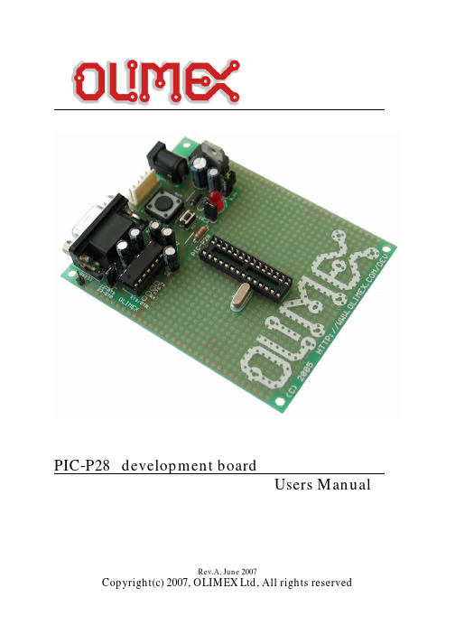
PIC-P28 development boardManualUsersRev.A, June 2007Copyright(c) 2007, OLIMEX Ltd, All rights reservedINTRODUCTION:PIC-P28 board is development board which allow you to prototype anddevelop code for all Microchip’s PIC microcontrollers with 28 pins.What you can do with PIC-P28? A lot of stuff let’s see what we have:PIC-P28 have RS232 connector and driver, so you can interface yourPIC microcontroller to other embedded or PC with RS232. The RS232driver have 4 lines Tx, Rx, CTS and jumper selectable RTS or DTR.The pin labeled RX is output and should be connected to PIC UART Tx.The pin labeled TX is input and should be connected to PIC UART Rx.Note that MAX232 driver on the socket is 5V device, so if you decideto run your PIC on 3.3V you should replace it with MAX3232 whichworks on 3.3VThe on-board ICSP connector allow you to program the PIC on theboard without pulling it of the socket, by ICSP programmer like PIC-MCP, PIC-MCP-USB, PIC-PG1, PIC-PG2, PIC-PG3, PIC-PG4 or toprogram and debug it with PIC-ICD2, PIC-ICD2-POCKET or PIC-ICD2-TINY. IMPORTANT: all programmers provide power supply throughICSP connector during the programming PIC-P18 should not bepowered via the external power jack!The power supply circuit have diode bridge after the power supply jackwhich allow you to power this board with both AC and DC power supplyadapters. The input voltage could be anything within the range +7.5 –15V DC or 6-12V AC.Voltage regulator is made with LM317 adjustable voltage regulator andhave jumper which selects what voltage you supply to the PICmicrocontroller +3.3V or +5V, so you can work with PICs on both lowand normal voltage.The oscillator circuit is made with 20 Mhz crystal oscillator, so youcan run your PIC at maximum performance.The RESET circuit is made with simple RC circuit and RESET pushbutton, the reason to not use RESET IC is that the board shouldsupport both 3.3V and 5V operation while RESET ICs are on fixedvoltage.PIC-P28 have user button for user input connected to PICmicrocontroller’s RA5 port. When RA5 port is initialized as INPUT youwill read “0” when the button is pressed and “1” when it is depressed.Status LED is connected via jumper to PIC microcontroller’s RA0 port.When your RA0 port is initialized as OUTPUT and set to “0” LED willgo ON, when RA0 port is set to “1” LED will go OFF.PIC-P28 have handy GND pin for connection to oscilloscope.FEATURES:•ICSP/ICD connector for programming and debugging•RS232 interface with MAX232 IC on socket•DIL28 microcontroller socket•Quartz crystal 20Mhz•LED to RA0 through jumper•user Button to RA5•Reset button and circuit•Power plug-in jack, accept AC and DC input•selectable +3.3V / +5V power supply voltage regulator (3.3V when jumper isclosed)•Extension slot on every uC pin•Gird 100 mils•GND bus•Vcc bus•Four mounting holes 3,3 mm (0,13")•FR-4, 1.5 mm (0,062"), green soldermask, white silkscreen component print•Dimensions 100x80 mm (3,9x3,15")All boards produced by Olimex are ROHS compliantDEMO1: PIC16F876-I/P BLINK LEDThis is demo code which blinks the LED on PIC-P28 board.Note:LED jumper should be closed!DEMO2: PIC16F876-I/P BUTTON readThis is demo code which show how to read BUTTON status and to switchthe LED ON when button is pressed and LED off when the button isdepressed.DEMO3: PIC16F876-I/P RS232 send / receive routinesThis is demo code, which show how to use the USART to send and receivecharacters from host PC via RS232 cable.The MAX232 by default is not connected to PIC on the board so you have tosolder two wires – one from RC6 (pin #17) of PIC16F876 Tx signal toMAX232 Tx labeled pin, and second from RC7 (pin #18) of PIC16F876 Rxsignal to MAX232 Rx labeled pin.You must program the HEX code to PIC16F876 and run the code.If you programmed the PIC correctly and wired the UART, when you openHyperterminal on your host PC computer with 9600 bps, 8 data bit, 1 stopbit, No flow control and apply power supply to the PIC-P28 every characteryou type on the hyperterminal will be printed back with “*” i.e. if you type“abc” you will receive “a*b*c*”.ORDER CODE:PIC-P28 – assembled and tested (no kit, no soldering required)PIC-P28/PCB – blank PCBs onlyHow to order?You can order to us directly or by any of our distributors.Check our web /dev for more info.Revision history:REV.A - create June 2007Disclaimer:© 2007 Olimex Ltd. All rights reserved. Olimex®, logo and combinations thereof, are registered trademarks of Olimex Ltd. Other terms and product names may be trademarks of others.The information in this document is provided in connection with Olimex products. No license, express or implied or otherwise, to any intellectual property right is granted by this document or in connection with the sale of Olimex products.Neither the whole nor any part of the information contained in or the product described in this document may be adapted or reproduced in any material from except with the prior written permission of the copyright holder.The product described in this document is subject to continuous development and improvements. All particulars of the product and its use contained in this document are given by OLIMEX in good faith. However all warranties implied or expressed including but not limited to implied warranties of merchantability or fitness for purpose are excluded.This document is intended only to assist the reader in the use of the product. OLIMEX Ltd. shall not be liable for any loss or damage arising from the use of any information in this document or any error or omission in such information or any incorrect use of the product.。
King4418开发板三星四核cortex-a9开发板最新方案选择
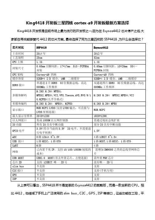
King4418开发板三星四核cortex-a9开发板最新方案选择King4418开发板是目前市场上最为流行的开发板之一,因为在Exynos4412芯片停产之后,大家都在寻找能够替代4412的芯片方案。
最终选择了同为三星四核的S5P4418,为什么会选择它?芯片对比S5P4418Exynos4412上市时间 2014年 2012年工艺制程 28nm 32nm CPU 主频 1.4G1.4G封装尺寸0.65mm 引脚间距,17*17mm 513-FCFBGA封装0.65mm 引脚间距,18*20mm 804-FCFBGA 封装CPU 架构 Cortex-A9 四核 Cortex-A9 四核缓存容量 32KB*4 I/D 缓存,1MB 二级缓存32KB*4 I/D 缓存,1MB 二级缓存 DDR3接口单通道2片DDR3 32位数据总线,高达800MHz 工作频率双通道四片DDR3 32位数据总线,高达800MHz 工作频率多媒体解码 H.263 H.264 MPEG1,MPEG2,MPEG4,VCI,VP8,Theora,AVS,RV8/9/10,MJPEG(几乎全格式)H.263 H.264 MPEG2,MPEG4,VCI 多媒体编码 H.263 H.264 MPEG4,MJPEGH.263 H.264 MPEG 显示接口RGB/MIPI/LVDS(支持LVDS 输出,可直接与LVDS 屏相连接)RGB,MIPI最大显示分辨率 2048*1280 1920*1200以太网接口 集成1000M 以太网控制器 需通过地址总线扩展 IO 功能 所有IO 具有中断功能部分IO 具有中断功能 GPIO 电平3.3V(符合当前的3.3V IO 电平,不需要进行电平转换)1.8VADC 8路12bit 0~1.8V 4路12BIT 0~1.8vUSB 接口 1路HSIC,1路OTG 1路HOST,1路HSIC,1路OTG UART 6路4路网络已内置千兆IP,支持10/100/1000M(较低的成本)需增加DM9000之类的总线型网络芯片USB HOST U SB2.0 HOST(省去外置芯片,方便连接) 需外置PHY 芯片 芯片ID 支持 128BIT 唯一 ID 号 没有唯一 ID 号 slim bus 不支持 支持C2C 接口 不支持 支持(手机专用) GPS 不支持 支持 ISP 不支持支持从上表可以看出,S5P4418并不是简单的Exynos4412的裁剪版,而是一款全新的CPU。
G4418 开发平台软硬件支持说明说明书
G4418开发平台软硬件支持说明深圳葡萄雨技术有限公司版权声明本手册版权归属深圳市葡萄雨技术有限公司所有,并保留一切权力。
非经葡萄雨技术有限公司同意(书面形式),任何单位及个人不得擅自摘录本手册部分或全部,违者我们将追究其法律责任。
技术支持如果您对文档有所疑问,您可以拨打技术支持电话或E-mail联系。
网址:/目录版权声明..........................................................................................错误!未定义书签。
第1章软件支持说明. (6)1.1产品简介 (6)第2章硬件外设支持说明 (8)2.1LCD屏 (8)2.2LVDS屏 (8)2.3MIPI屏 (8)2.4触摸IC (9)2.5并口摄像头 (9)2.6MIPI摄像头 (9)2.7TVIN (9)2.8USB摄像头 (9)2.9PCIE3G (9)2.10PCIE4G(全网通) (10)2.11USB3G dongle (10)2.12USB WIFI (10)2.13USB蓝牙 (10)2.14音频芯片 (10)2.15NFC(非接) (11)2.16GPS/北斗 (11)2.17工作温度 (11)2.18其它 (11)第3章产品线介绍 (12)3.1核心板系列 (12)3.2开发板系列 (12)3.3卡片电脑系列 (12)第1章软件支持说明1.1产品简介Gbox4418卡片电脑支持android4.4.2操作系统,linux3.4.39+QT5.4系统以及ubuntu12.04三大操作系统。
各操作系统支持的驱动列表如下:第2章硬件外设支持说明以下描述为在G4418开发平台上验证过的的部分外设模块;根据客户需求,可以为客户提供选型帮助。
2.1LCD屏7寸高清屏:VS070CXN,1024x600,RGB;7寸标清屏:AT070TN92,1024x600,RGB;5寸屏:HSD050IDW1,800x480,RGB;4.3寸屏:AT043TN24,480x272,RGB;2.8寸屏:TM028HBHG53,240x320,SPI+RGB;2.2LVDS屏11.6寸:b116xtn04,1366x768;10.1寸:BP101WX7,1280x800;claa101nc05,1024x600;YH101IF40-A,1024x600;8寸:ej080na,1024x768;5.6寸:HV056WX2,1280x800;2.3MIPI屏7寸:WY070ML,1024x600;5.5寸:NST500HD,720x1080;TS8055PC,长虹T806,720x1280;2.4触摸IC电容触摸:GSL1680,GSL3680,GT9XX,FT6X36,FT5X06;电阻触摸:TSC2003,TSC2007;2.5并口摄像头30万像素:SP0838;200万像素:SP2518,GC2035;500万像素:HM5065(带自动对焦);2.6MIPI摄像头500万像素:OV5645(带自动对焦);2.7TVINTVP5150;2.8USB摄像头200万像素:罗技C270;2.9PCIE3GCWM900;MU609;2.10PCIE4G(全网通)EC20;UC20;2.11USB3G dongleE303C(CDMA2000);E1750(WCDMA);2.12USB WIFIRTL8723BU;RTL8188EU;2.13USB蓝牙RTL8723BU;2.14音频芯片ALC5621;WM8960;2.15NFC(非接)PN544;2.16GPS/北斗G591;(单GPS)中科微北斗/GPS双模;2.17工作温度-35度到+80度;2.18其它待补充;第3章产品线介绍3.1核心板系列G4418(主控为三星4418)G6818(主控为三星6818)G210(主控为三星210)M9核心板(主控为高通8916)3.2开发板系列G4418开发板(主控为三星4418)G6818开发板(主控为三星6818)G210开发板(主控为三星210)M9开发板(主控为高通8916)3.3卡片电脑系列G4418卡片电脑(主控为三星4418)G6818卡片电脑(主控为三星6818)G3188卡片电脑(主控为瑞芯微3188)说明:产品详细规格,以及更多其他产品请关注葡萄雨技术官方网站或与我们联系。
三星四核S5P4418开发板RP4418使用说明及功能测试

三星四核S5P4418开发板RP418使用说明及功能测试RP4418开发板是深圳荣品电子科技采用S5P4418 主芯片研发设计的一款稳定性强、可靠性高的成熟三星四核方案产品,整合了目前电子、航海、车载、消费、娱乐、工业等行业常用接口,满足常规功能。
MID,POS,PDA,PND,智能家居,手机,车机,学习机,游戏机以及其他各种工控领域。
开发板默认搭载Android5.1系统,支持500W摄像头MIPI接口的OV5645;支持蓝牙4.0功能、WiFi+LAN+4G无缝联网、GPS全球定位;另还有Linux+QT4.8及Ubuntu12.04系统,性能与体验的极致发挥。
本篇主要是拿到4418开发板后的功能使用测试。
1、RP4418开发板开机现在4418平台已升级为上电自启动,即插上电源线板子就会启动了,不需要再按开机键。
如果想要上电按键再开机,可以在购买时就联系荣品厂家修改。
以下是说的上电须按开机键的。
电源线请不要插12V,很多朋友都是插错电源线,导致开发板不能开机。
1)将荣品提供的电源适配器(5V/3A)插入电路板,将DC头插入开发板的插孔(Power Input);2)按住Power KEY键3秒钟后松手,开发板即可启动。
启动以后,LED红灯会变亮。
2、LCD显示开机后LCD正常显示主要验证左上角,右上角,底部虚拟按键栏这几个位置的对齐。
3、触摸屏如果开机后触摸正常解锁,按到特定位置有响应,说明触摸正常。
4、WiFi要验证WIFI模块,首先打【设置】;接着把WIFI按钮打开。
选择AP进行连接(和手机连WiFi一样),连接成功后,会显示已连接,且状态栏WIFI的连接图标。
5、蓝牙4.0蓝牙和WIFI一样,在【设置】里打开。
会自动搜索附近的蓝牙设备。
我们可以看到右上角有蓝牙打开的图标,我们设备也显示出来了(MEIZU PRO 5)。
接着我们搜索蓝牙设备进行配对和手机使用蓝牙配对一样,输入正确配对码后就可以进行传输文件了。
WP-8x4x系列控制器1.4.1.0版本发布说明书

WP – 8X4X Version 1.4.1.0 Release Note OverviewThe latest version of OS image and Eboot can be updated to WP-814x/WP-844x/WP-884x series controller.SDHC driver replaces the original SD driver. Compared to the previous driver, The microSD capacity can be supported to 32 GB and the read/write performance of SD will be enhanced in new driver.Support SDHC (Maximum size: 32GB)WP-8x4x series supports 3 OS imageMulti-languageEnglishGermanRussianSimplified ChineseTraditional ChineseWINPAC270_yyyymmdd_Ver.x.x.x.x_xx.bin changed toWPpppp__yyyymmdd_Ver.n.n.n.n_xx.binWINPAC270_yyyymmdd_Ver.x.x.x.x_xx.exe changed toWPpppp__yyyymmdd_Ver.n.n.n.n_xx.exesqlceca35.dllsqlcecompact35.dllsqlceer35en.dllsqlceme35.dllsqlceoledb35.dllsqlceqp35.dllsqlcese35.dllGAC_System.Data.SqlServerCe_v3_5_0_0_cneutral_1.dllSystem.Data.SqlClient.dllSystem.Data.SqlServerCe.dllHow to How to use Multi language use Multi language use Multi language OS OSChoose multi-language user interfaceClick “Control Panel” from Start menu and Click Regional Settings iconClick “language” tab and choose “Russian” for User interface language.Click “OK”Run WinPAC utility and click “Save and Reboot” to save the UI language.After reboot, the interface language is in Russian. (The menus, dialogs and alerts will be shown in Russian.How to update How to update Eboot and OS Eboot and OSRefer to E.1. How to upgrade for WinPAC-8000 onWinPAC_8000_user_manual_v1.x.pdf for more detail to updating the Eboot and OS.Important NotesWinPAC SDK WinPAC SDK Header files and library files for desktop Header files and library files for desktop Header files and library files for desktopWinPACSDK (PAC270_SDK.msi) provided an application developer with the information necessary to develop an EVC or .Net Framework application specifically for WinPAC.Update PAC270_SDK.msiInstall SDK for developing EVC application Click CustomClick NextInstall SDK for developing EVC and .Net Framework application Click Complete buttonImportant NotesClick Directories tab on the Tools -> Options and add “C:\Program Files\Windows CE Tools\wce500\PAC270\ ICPDAS\Include\ARMV4I” to“Directories:” belowAdd C:\Program Files\Windows CE Tools\wce500\PAC270\ ICPDAS\Lib\ARMV4I to “Directories:” belowFinish the actions above, and then click “OK” button.Build the project again, and the project can be built successfully.Deploy warningIf the Error message box appear while the user’s EVC program is deployed to WinPAC device using cemgrc.exe. Please install thePAC270_SDK_20090624.msi to fix this problem.Debug WinPAC programs in Visual Studio 2005/2008 Debug WinPAC programs in Visual Studio 2005/2008The OS image version of the WinPAC series must be V1.3.0.4 or later, and PAC270_SDK_20090225.msi must be installed on the PC.The following steps are how debugs .Net CF program in VS2005/VS2008 Step 1: Copy the following files to \System_Disk\ICPDAS\System folder on WinPAC-8000C lientshutdown.exeC onmanClient2.exeC Maccept.exee DbgTL.dllT cpConnectionA.dllBefore copying these files to WinPAC-8000, make sure these files below are the same version.For exampleFor exampleThe version number of all the files below is 8.0.50727.421. C:\Program Files\Common Files\MicrosoftShared\CoreCon\1.0\Target\wce400\armv4i2. C:\Program Files\Common Files\Microsoft Shared\CoreCon\1.0\Bin3. C:\Program Files\Common Files\Microsoft Shared\CoreCon\1.0\Bin\10334. Right click the file and click properties to check the clientshutdown.exe/CMAccept.exe/ConmanClient2.exeSelect the “Version” tab and Check the File VersionStep 2: On the “Project” menu, click “[Project Name] Properties…”commandStep 3: On the “SystemInfo*”tab, unselect “Deploy the latest version of the .NET compact Framework (includeing Service Packs)”check boxStep 4: On the “Tools”menu, click “Options…”commandStep 5: On the “Options”dialog, select “PAC 270”from the “Showdevices platform”list, and then click the “Properties…”buttonStep 6: On the “PAC50- ARMV4:ARMV4I_Release Properties”dialog, click the “Configure…”buttonStep 7: On the “Configure TCP/IP Transport”dialog, select the “Usespecific IP address”option and type the IP address of WinPAC-8000, and then click the “OK”buttonStep 8: On the “PAC50- ARMV4:ARMV4I_Release Properties”dialog, click the “OK”buttonStep 9: On the “Options”dialog, click the “OK”buttonStep 10: On the WinPAC-8000 controller side, run the “CommanClient2”and the “CMAccept.exe”applications which is located at:\System_Disk\ICPDAS\SystemStep 11: On the “Tools”menu, click “Connect to Device…”commandStep 12: On the “Connect to Device” dialog, select “PAC 270” from “Platform” list and then click the “Connect” buttonStep 13: On the “Tools”menu, click “Connect to Device…”commandStep 14: Connection established. Then you can debug on line.FAQ:If the connection fails shown as follow, Return to Step 10 to do the action belowRun the “ConmanClient2.exe /transport:tcpconnectiona.dll /property:port=5000 /id:Con ”at: \System_Disk\ICPDAS\System, and then run the “CMAccept.exe”The port number defined on Property:port=5000 must be same with the setting on Step7 (Check “Use fixed port number” and set to 5000)Note:The CommanClient2.exe must run before running CMAccept.exe.Support Support l l arge arge software Key board software Key board software Key board The original software keyboard is as followThe large Keyboard is shown as follow。
- 1、下载文档前请自行甄别文档内容的完整性,平台不提供额外的编辑、内容补充、找答案等附加服务。
- 2、"仅部分预览"的文档,不可在线预览部分如存在完整性等问题,可反馈申请退款(可完整预览的文档不适用该条件!)。
- 3、如文档侵犯您的权益,请联系客服反馈,我们会尽快为您处理(人工客服工作时间:9:00-18:30)。
2.4.17 复位按钮.........................................................................................................15
淘宝:
QQ 群: x4412 技术论坛: 【16073601】 x4418 技术论坛: 【199358213】 x210 技术论坛 1: 【23831259】 x210 技术论坛 2: 【211127570】 x210 技术论坛 3: 【211128231】 i210 技术论坛 1: 【159144256】 i210 技术论坛 2: 【189920370】
2.3.8 U451(camera 接口)......................................................................................... 11
2.3.9 LCD1(LCD&VGA 接口) ...............................................................................12
2.1
硬件接口描述 ........................................................................................................... 6
2.2
开发板启动指引 ....................................................................................................... 8
版本说明
版本号 Rev.01
日期 2015-4-28
作者 lqm
原始版本
描述
技术支持
如果您对文档有所疑问,您可以在办公时间(星期一至星期五上午 9:00~12:00;下午 1:30~6:00)拨打技术支持电话或 E-mail 联系。
网 址: 论 坛: 联系电话: 0755-33121205 0755-33133436 E-mail: supports@
2.4.1 电源开关和插座.............................................................................................13
2.4.2 调试串口.........................................................................................................13
X4412 Linux平台
用户手册
深圳市九鼎创展科技有限公司
版权声明
本手册版权归属深圳市九鼎创展科技有限公司所有, 并保留一切 权力。非经九鼎创展同意(书面形式),任何单位及个人不得擅自摘录 本手册部分或全部,违者我们将追究其法律责任。
敬告: 在售开发板的手册会经常更新,请在 网 站下载最新手册,不再另行通知。
2.4.11 独立按键.........................................................................................................14
2.4.12 调试 LED 灯 ...................................................................................................15
2.3
扩展接口定义 ........................................................................................................... 8
2.3.1 核心板引脚定义 1............................................................................................8
2.4.13 电源指示灯.....................................................................................................15
2.4.14 USB OTG 接口...............................................................................................15
目录
版权声明........................................................................................................................ 2
第 1 章 x4418 开发板简介 ..........................................................................................3
2.4.7 喇叭接口.........................................................................................................14
2.4.8 录音接口.........................................................................................................14
2.3.10 J38(电源输出接口).........................................................................................12
2.4
硬件接口 ................................................................................................................. 13
2.4.15 USB HOST 接口.............................................................................................15
2.4.16 开机按钮.........................................................................................................15
2.4.9 拨码开关.........................................................................................................14
2.4.10 TF 卡槽 ...........................................................................................................14
2.3.2 核心板引脚定义 2............................................................................................9
2.3.3 核心板引脚定义 3............................................................................................9
1.1
android4.4 系统 ........................................................................................................4
1.2
产品简介 ................................................................................................................... 4
2.4.5 以太网接口.....................................................................................................13
2.4.6 耳机接口.........................................................................................................14
销售与服务网络
公司:深圳市九鼎创展科技有限公司 地址:深圳市宝安中心区兴业路宝安互联网产业基地 B 区 3003B 室 邮编:518101 电话:0755-33121205 0755-33133436 网址: 论坛:
2.4.3 HDMI 接口 .....................................................................................................13
2.4.4 camera 接口 ....................................................................................................13