System block diagram(Main)
机械手的系统工作原理及检测传感装置构成的总结与分析
机械手的系统工作原理及检测传感装置构成的总结与分析1.引言1. Introduction近20年来,气动技术的应用领域迅速拓宽,尤其是在各种自动化生产线上得到广泛应用。
电气可编程控制技术与气动技术相结合,使整个系统自动化程度更高,控制方式更灵活,性能更加可靠;气动机械手、柔性自动生产线的迅速发展,对气动技术提出了更多更高的要求;微电子技术的引入,促进了电气比例伺服技术的发展。
现代控制理论的发展,使气动技术从开关控制进入闭环比例伺服控制,控制精度不断提高;由于气动脉宽调制技术具有结构简单、抗污染能力强和成本低廉等特点,国内外都在大力开发研究。
Over the past 20 years, the application of pneumatic technology fields expand rapidly, especially widely used in all kinds of automatic production line. Electrical programmable control technology combined with pneumatic technology, automation degree higher, the whole system control method is more flexible, more reliable performance; Pneumatic manipulator, the rapid development of flexible automatic production line of pneumatic technology is put forward more higher requirement; The introduction of microelectronics technology, promote the development ofelectric proportional servo technology. Pneumatic technology from the development of modern control theory, the switch control in closed loop proportional servo control, improving control precision; Because the gas artery width modulation technique has simple structure, strong ability to resist pollution and low cost etc., are vigorously develop research at home and abroad.2.气动技术发展状况及优缺点2. The pneumatic technology development status and the advantages and disadvantages气动技术是一门正在蓬勃发展的新技术,气动元件是气动技术中最重要的组成部分,用气动元件组成的传动和控制系统己广泛应用于国民经济各部门的成套设备和自动化生产线上。
主板架构及硬体知识

如果是Intel chipset, 因為產品種類多, 為避免衝突, 則不一定會在第一個字, 如 845 系列早期Intel 內部稱呼為Brookdale, 我們就取P4'B'. 另一個865系列 (Springdale), 因為不可能取名P4„S‟, 這樣會和SIS的機種 衝突, 於是取第二個字'P', 就是P4P800系列. 875則因為原名Canterwood, 所以取'C'叫作P4C800系列. 915系列(Grantsdale)就是P5GD1, 925X(Alderwood)就是P5AD2. 至於其他3rd party的chipset則因為機種數較少, 都直接取公司名, 如P4S800 (SIS), P4V8X-X (VIA), K8N (Nvidia), P4U800-X (ULI).
Socket 754是2003年9月AMD64位桌面平台最初发布时的CPU接 口,目前采用此接口的有低端的Athlon 64和高端的Sempron,具有754 根CPU针脚。
第二部分: CPU辨别 Socket 939 Socket 939是AMD公司2004年6月才推出的64 位桌面平台接口标准,目前采用此接口的有高端的 Athlon 64以及Athlon 64 FX,具有939根CPU针脚。
第一部分
第四個字以後常常接了數字, 有時是代表FSB, 有時是DDR的速度, 有時 是AGP的速度, 不一定會是哪一個,原則是先考慮FSB, 如果沒啥特別再 考慮AGP, 最後才是DDR速度.如P4P800, P4C800, P4S800, P4V800-X 都代表support FSB800. 再來是8X, P4V8X-X, A7V8X-X, 因為他們的FSB都沒啥特別的或規格 不夠新潮(如次一級的FSB533), 就會退而求其次 還有些機種是以DRAM的速度命名, 如P4S133, P4S333,A7V266, A7S266-VM, ...這是因為他們的FSB, AGP速度都不是最新規格, 所以用 DRAM速度來區分. 之外還有很多特例, 如P4V880, 是因為chipset 名稱叫作PT880, 並非support FSB880.A7V600, 是因為chipset叫KT600,
直流润滑油泵控制箱中英文说明书(操作说明书)
JY-ZK IntelligentJY-ZK智能型DC MotorControl Cabinet直流电机控制箱Operation Manual使用说明书Shaanxi Jinyuan Automation Technology Co., Ltd.XX金源自动化科技XX一、Overview概述JY-ZK Intelligent DC motor control cabinet lubricating products are aimed at generating power plant system design a new type of lubricant replacement products, mainly used for steam turbine and generator of the main bearings, thrust bearing and the disk devices to provide lubricating oil vehicle control, as well as the generator seal oil system provides oil to ensure the safe operation of the pressure of the oil control. Generator control system equipment lubricants usually are:lubricating oil tank, main oil pumps, AC lubricating oil pump (#1 machine 2 Units), Oiler,and Oil cooler, emergencyDC pumps, jacking oil pumpsystem, oil-fume separatedevices andpurifyingSystem and so on. In normal operation, all the lubricant oil supply from the main oil pump. When the main pump failure resulted in reduced a certain value, AC, DC lubrication pump automatically linkage.JY-ZK智能型直流润滑电机控制箱系列产品是针对发电厂发电机润滑油系统设计的新型换代产品,主要用于汽轮机和发电机各主轴承、推力轴承和盘车装置提供润滑油的控制,以及对发电XX封油系统提供油源,确保系统平安运行的压力油控制。
sobel算子图像边缘检测研究外文翻译

Real-time FPGA Based Implementation of ColorImage Edge DetectionAbstract—Color Image edge detection is very basic and important step for many applications such as image segmentation, image analysis, facial analysis, objects identifications/tracking and many others. The main challenge for real-time implementation of color image edge detection is because of high volume of data to be processed (3 times as compared to gray images). This paper describes the real-time implementation of Sobel operator based color image edge detection using FPGA. Sobel operator is chosen for edge detection due to its property to counteract the noise sensitivity of the simple gradient operator. In order to achieve real-time performance, a parallel architecture is designed, which uses three processing elements to compute edge maps of R, G, and B color components. The architecture is codedusing VHDL, simulated in ModelSim, synthesized using Xilinx ISE 10.1 and implemented on Xilinx ML510 (Virtex-5 FX130T) FPGA platform. The complete system is working at 27 MHz clock frequency. The measured performance of our system for standard PAL (720x576) size images is 50 fps (frames per second) and CIF (352x288) size images is 200 fps.Index Terms—Real-time Color Image Edge Detection, Sobel Operator, FPGA Implementation, VLSI Architecture, Color Edge Detection ProcessorI. INTRODUCTIONHigh speed industrial applications require very accurate and real-time edge detection. Edge detection in gray images does not give very accurate results due to loss of color information during color to gray scale image conversion. Therefore, to achieve desired accuracy, detection of edges in color images is necessary. The main challenge for real-time implementation of color image edge detection is in processing of high volume of data (3 times as compared to gray images) within real-time constraints. Therefore, it is hard to achieve real-time performance of edge detection for PAL sizes color images with serial processors. Due to inherent parallelism property, FPGAs can deliver real-time time performance for such applications. Furthermore, FPGAs provide the possibility to perform algorithm modifications in later stages of the system development [1].The main focus of most of the existing FPGA based implementations for edge detection using Sobel operator has been on achieving real-time performance for gray scale images by using various architectures and different design methodologies. As edge detection is low-level image processing operation, Single Instruction Multiple Data (SIMD) type architectures [2] are very suitable for edge detection to achieve real-time performance. These architectures use multiple data processing elements and therefore, require more FPGA resources. The architecture clockfrequency can be improved by using pipelining. A pipelined architecture for real-time gray image edge detection is presented in [3]. Some computation optimized architectures are presented in [4, 5]. Few more architectures for real-time gray image edge detection are available in [6 - 11]. In [12, 13], the architectures are designed using MA TLAB-Simulink based design methodology.In this paper, we show that real-time Sobel operator based color image edge detection can be achieved by using a FPGA based parallel architecture. For each color component in RGB space, one specific edge computation processor is developed. As Sobel operator is sliding window operator, smart buffer based Memory architecture is used to move the incoming pixels in computing window. The specific datapaths are designed and controller is developed to perform the complete task. The design and simulation is done using VHDL. The design is targeted to Xilinx ML 510 (Virtex –5 FX130T) FPGA platform. The implementation is tested for real world scenario. It can robustly detect the edges in color images.The rest of the paper is organized in the following way . In section 2 we describe the original Sobel operator based edge detection algorithm. We show, in section 3, the customized architecture for algorithm implementation and how each stage works. In section 4, practical tests are evaluated and synthesis results are shown taking into account system performance. Finally conclusions anddiscussions are presented in section 5.II. EDGE DETECTION SCHEMEIn this section the used algorithm is briefly described, for a more detailed description we refer to [14, 15]. The Sobel operator is widely used for edge detection in images. It is based on computing an approximation of thegradient of the image intensity function. The Sobel filter uses two 3x3 spatial masks which are convolved with the original image to calculate the approximations of thegradient. The Sobel operator uses two filters Hx and Hy.⎥⎥⎥⎦⎤⎢⎢⎢⎣⎡---=101202101X H (1)⎥⎥⎥⎦⎤⎢⎢⎢⎣⎡=1211001-2-1-y H (2)These filters compute the gradient components across the neighboring lines or columns, respectively. The smoothing is performed over three lines or columns before computing the respective gradients. In this Sobel operator, the higher weights are assigned in smoothing part to current center line and column as compared to simple gradient operators. The local edge strength is defined as the gradient magnitude given by equation 3.()22,Hy Hx y x GM += (3)This equation 3 is computationally costly because of square and square root operations for every pixel. It is more suitable computationally to approximate the square and square root operations by absolute values.()Hy Hx y x GM +=, (4)This expression is much easy to compute and still preserves the relative changes in intensity (edges in images).This above mentioned scheme is for gray scale images. For color images (RGB color space) this scheme is applied separately for each color component. Final color edge map of color image is computed by using the edge maps of each color component [16].)(B Edge or G Edge or EdgeR ColorEdge (5)III. PROPOSED ARCHITECTURETo detect edges in real-time in PAL (720x576) size color images, dedicated hardware architecture is implemented for Sobel operator based edge detection scheme. Fig. 1 shows the conceptual block diagram of complete system. The hardware setup includes a video camera, a video daughter card, and FPGA board. The video output of camera connects to Digilent VDEC1 Video Decoder Board which is interfaced with Xilinx ML510 (V irtex –5 FX130T) board using Interface PCB. Display Monitor is connected to the board using DVI connector. The video signals are decoded in Camera Interface Module. The output RGB data of camera interface module is applied to edge detection block. The edge detected output from the Edge Detection Block is displayed on the display monitor using DVI controller. The camera interface module also generates video timing signals which are necessary for proper functioning of edge detection block and DVI controller. A more detailed description of this Camera Interface Design can be found in[17].Figure 1. Complete System Block DiagramFig. 2 shows the basic block level data flow diagram for computation of edges in color images using Sobel operator. The goal is to perform edge detection three times, once each for red, green, and blue, and then the output is fused to form one edge map [16]. There are mainly four stages. First stage is Buffer Memory stage. In this stage, the three color components are separated andstored in three different memories. The second stage is gradient computation stage. In this stage the gradient is computed for each color component by adding absolute values of horizontal and vertical gradients. In third stage, the edge map is computed for each color component by comparing the gradient values with threshold. Final edge map is computed by combining the edge maps of each color components in stage four.Figure 2. Edge Detection in Color Images using Sobel OperatorThe streaming data processing cannot be used because the edge detection using Sobel operator algorithm is window based operation. Therefore, input data from camera is stored in on-chip memory (BRAM and Registers) before processing it on FPGA. The Sobel edge detection logic can begin processing as soon as two rows arrived in Buffer Memory. The Smart Buffer based Buffer Memory architecture [18] is used in the proposed Sobel operator based color edge detection implementation for data buffering. This approach (Fig. 3) works if one image pixel is coming from camera interface module in one clock cycle. The pixels are coming row by row. When buffers are filled, this architecture provides the access to the entire pixel neighborhood every clock cycle. The architecture places the highest demand on internal memory bandwidth. Because modern FPGA devices contain large amount of embedded memory, this approach does not cause problems [19]. The length of the shift registers depends on the width of input image. ForPAL (720x576) size images the length of FIFOs is 717 (i.e. 720 - 3). For CIF (352x288) size images, it is 349 (i.e. 352 – 3).Figure 3. Sliding Window Memory Buffer ArchitectureThe absolute values of gradient Hx and Hy for pixel data P2,2 is given by following expressions.())())*21333123,21,13,1,,,((P P P P P P Hx -+-+-= (6)())())*23,1332,12,31,11,3P P P P P P Hy -+-+-=,(( (7)The processing modules architectures for computing these horizontal and vertical gradients for each color components are shown in Fig. 4. Both the architectures are same except the inputs applied to them at a particular time. Each processing module performs additions, subtractions, and multiplication. The multiplication is costly in digital hardware but multiplication by 2 is easily achieved by shift operation.The complete architecture (Fig. 5) uses three processing elements in parallel (each for R, G , and B color components). The data coming from camera interface module is 24-bit RGB data. Incoming data is separated in three color components R, G , and B. Each color component data is of 8-bit (i.e. any value from 0 to 255). Three smart buffer based Sliding Window Memories are used to store two rows of the three color components. Each memory uses two First-in First-out (FIFO) shift-registers and 9 registers. The width of FIFOs and registers is 8-bit. Therefore, in total 6 FIFOs and 27 registers are required for designing Sliding Window Buffer Memory for RGB color image edge detection architecture. The designing of FIFOs using available registers in FPGA occupies large area in FPGA. Therefore, available Block RAMs on FPGA are used for designing the FIFOs. This resulted in efficient utilization of FPGA resources.Figure 4. Gradient Hx and Hy Computation Module ArchitecturesFor detecting edge in PAL (720x576) size color images, it takes 1440 (720x2) clock cycles to fill the two rows of image data in buffer memory. After this, in every clock cycle, each color component (R, G , and B) of new pixel is moved in their respective computing window (consists of 9 registers). The available 9 pixels in computing window (P1,1, P1,2, P1,3, P2,1, P2,2, P2,3, P3,1, P3,2, P3,3) are used for computing the Hx and Hy gradient values. These are computed according to equations 6 and 7 by using the processing module architectures shown in Fig 4. The approximate magnitude of the gradient is computed along each color component by adding the absolute values of Hx and Hy. After this, the approximate gradient of each color component is compared with a user defined threshold value. If the approximate value of gradient is more than the user defined threshold, the comparator output for that color component is 1 else it is 0. Theoutputs of all three comparators (R, G, and B) are finally fused to find the final edge map. The final edge map is computed by ORing the Edge Map outputs of each color component. It requires one three input OR gate. If the final edge map output is one, the each color component value is set to 11111111 else it is set to 00000000. These values are used by DVI controller to display the result on display Monitor.Figure 5. Complete Architecture for Color Image Edge Detection using Sobel OperatorIV. RESULTSThe proposed architecture is designed using VHDL and simulated in ModelSim. Synthesis is carried out using Xilinx ISE 10.3. Final design is implemented on Xilinx ML510 (Virtex–5 FX130T) FPGA board. It utilizes 294 Slice Registers, 592 Slice LUTs, 206 FPGA Slices, 642 LUT Flip Flop Pairs, 116 Route-thrus and 3 Block RAMS. The synthesis results (Table I) reveal that the FPGA resources utilized by proposed architecture are approximately 1% of total available resources. The FPGA resource utilization table is only for proposed color image edge detection architecture (i.e. buffer memory, gradient computation, edge map computation) and excludes the resources utilized by camera interface and display logic. The measured performance of our system at 27 MHz operating frequency for PAL (720x576) size images is 50 fps (frames per second), CIF (352x288) size images is 200 fps and QCIF (176x144) size images is 800 fps. PAL and CIF images are most commonly used video formats. Therefore, implemented system can easily detect edges in color images in real-time.TABLE I. SYNTHESIS RESULTSFigure 6. Input Color Image and Output Edge Detected ImageFigure 7. Input Color Image and Output Edge Detected ImageFigure 8. Input Color Image and Output Edge Detected ImageFigure 9. Complete SystemIn Fig. 6-8, the input PAL (720x576) size color test images taken from camera and respective output edge detected images produced by proposed architectures are shown. Fig. 9 shows the complete system. The images are captured by using Sony EVI D70P analog camera, processed by designed VLSI architecture running on FPGA, and displayed on monitor.V. CONCLUSIONIn this paper, the hardware architecture for Sobel operator based color image edge detection scheme has been presented. The architecture used approximately 1% of total FPGA resources and maintained real-time constraints of video processing. The system is tested for various real world situations and it robustly detects the edge in real-time with a frame rate of 50 fps for standard PAL video (60 fps for NTSC video) in color scale. The speed could be further improved by adding pipelining stages in gradient computation modules at the expense of increasing FPGA resources usage. The Xilinx ML510 (Virtex-5 FX130T) FPGA board is chosen for this implementation due to availability of large number of FPGA resources, Block RAMs, and PowerPC processor (for hardware-software co-design) so that same board can be used to implement other complex computer vision algorithms which make use of edge detection architecture. The proposed architecture is very suitable for high frame rate industrial applications. The future work will look at the use of this architecture for finding the focused areas in a scene for surveillance applications.A CKNOWLEDGMENTThe authors express their deep sense of gratitude to Director, Dr. Chandra Shekhar, forencouraging research and development. Also the authors would like to express their sincerethanks to Dr. AS Mandal and Group Leader, Raj Singh,for their precious suggestions in refining the research work. Authors specially thank Mr. Sanjeev Kumar, Technical Officer, for tool related support. We thank to reviewers, whose constructive suggestions have improved the quality of this research paper.REFERENCES[1] H. Jiang, H. Ardo, and V. Owall (2009), A Hardware Architecture for Real-Time Video Segmentation Utilizing Memory Reduction Techniques, IEEE Transactions on Circuits and Systems for V ideo Technology, vol. 19, no. 2, pp. 226–236.[2] R.L. Rosas, A.D. Luca, and F.B. Santillan (2005), SIMD Architecture for Image Segmentation using Sobel Operators Implemented in FPGA Technology, In Proceedings of 2nd International Conference on Electrical and Electronics Engineering, pp. 77-80.[3] T.A. Abbasi and M.U. Abbasi (2007), A Novel FPGA-based Architecture for Sobel Edge Detection Operator, International Journal of Electronics, vol. 94, no. 9, pp. 889-896, 2007.[4] Z.E.M. Osman, F.A. Hussin, And N.B.Z. Ali (2010a), Hardware Implementation of an Optimized Processor Architecture for Sobel Image Edge Detection Operator, In Proceeding of International Conference on Intelligent and Advanced Systems (ICIAS), pp. 1-4.[5] Z.E.M. Osman, F.A. Hussin, And N.B.Z. Ali (2010b), Optimization of Processor Architecture for Image Edge Detection Filter, In Proceeding of International Conference on Computer Modeling and Simulation, pp. 648-652[6] I. Y asri, N.H. Hamid, And V.V. Y ap (2008), Performance Analysis of FPGA based Sobel Edge Detection Operator, In Proceedings of International Conference on Electronic Design, pp. 1-4. [7] V. Sanduja and R. Patial (2012), Sobel Edge Detection using Parallel Architecture based on FPGA, International Journal of Applied Information Systems, vol. 3, no. 4, pp. 20-24.[8] G. Anusha, T.J. Prasad, and D.S. Narayana (2012), Implementation of SOBEL Edge Detection on FPGA, International Journal of Computer Trends and Technology, vol. 3, no. 3, pp. 472-475. [9] L.P. Latha (2012), Design of Edge Detection Technique Using FPGA(Field Programmable Gate Array) and DSP (Digital Signal Processor), VSRD International Journal of Electrical, Electronics & Communication Engineering, vol. 2, no. 6, pp. 346-352.[10] A.R. Ibrahim, N.A. Wahed, N. Shinwari, and M.A. Nasser (2011), Hardware Implementation of Real Time Video Edge Detection With Adjustable Threshold Level (Edge Sharpness) Using Xilinx Spartan-3A FPGA, Report.[11] P.S. Chikkali and K. Prabhushetty (2011), FPGA based Image Edge Detection and Segmentation, International Journal of Advanced Engineering Sciences and Technologies, V ol. 9, Issue 2, pp. 187-192.[12] R. Harinarayan, R. Pannerselvam, M.M. Ali, And D.K. Tripathi (2011), Feature extraction of Digital Aerial Images by FPGA based implementation of edge detection algorithms, In Proceedings of International Conference on Emerging Trends in Electrical and Computer Technology, pp. 631-635.[13] K.C. Sudeep and J. Majumdar (2011), A Novel Architecture for Real Time Implementation of Edge Detectors on FPGA, International Journal of Computer Science Issues, vol. 8, no. 1, pp. 193-202.[14] W. Burger and M.J. Burge (2008), Digital Image Processing: An Algorithmic Introduction Using Java, New Y ork: Springer, 120-123.中文翻译:基于FPGA的实时彩色实现图像边缘检测Sanjay Singh Saini *,阿尼尔库马尔,拉维赛尼IC设计组CSIR中央电子工程研究所,拉贾斯坦,印度333031个学位-。
温度监测中英文翻译
土壤温度测量的设计1. 简介温度是土壤的一个十分重要的环境因素,它直接影响微生物的活跃性及有机物的分解,影响植物的根吸收水分与矿物质,同时它在植物生长率及根的范围上发挥着重要作用。
据统计,植物的根一般在地下50厘米范围内,因此测量这一范围内不同深度的土壤温度变得十分有意义。
目前,土壤温度测量仪器可分为三类。
第一种,是利用热敏电阻与土壤温度之间的关系测量实际温度。
在使用这类仪器前,系统参数需要校正,同时当解决系统遇到的问题时,十分不便。
第二种是非接触式的土壤测温仪器,它通过红外线测量温度,这种设备价格昂贵。
第三种,通过数字温度计测量温度。
目前,这类仪器不仅可测量一点的土壤温度,还可将数据进行存储与传输。
总之,上述设备因为价格过于昂贵或功能过于简单,而得不到广泛应用。
因此,一种价格更廉价,更能更强大的仪器需要去开发设计。
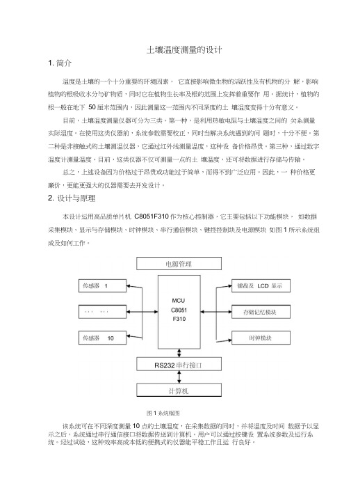
2. 设计与原理本设计运用高品质单片机C8051F310作为核心控制器,它主要包括以下功能模块,如数据采集模块、显示与存储模块、时钟模块、串行通信模块、键控控制块及电源模块如图1所示系统组成及如何工作。
图1系统框图该系统可在不同深度测量10点的土壤温度,在采集数据的同时,并将温度及时间数据予以显示之后,系统通过串行通信接口将数据传送到计算机。
用户可以通过按键设置系统参数及运行系统。
经过试验,这种效率高成本低的便携式的仪器能平稳工作且运行良好。
2.1硬件设计在硬件设计中,系统可利用的部分包括C8O51F310单片机、DS18B2C数字温度传感器、ISL6292可编程锂电池充电管理芯片、NCP500电压管理芯片以及DS1302时钟芯片,它们通过相应的外围电路连接在一起,同时这几部分是系统的核心结构。
下面就介绍这些核心部分及其外围电路。
2.1.1高质量C8051F310单片机C8051F310是一款兼容8051指令集的完全集成的混合信号ISP型MCU芯片。
C8051F31C主要由CIP-51内核、外围模拟电路、数字I/O 口及电源模块组成。
自动控制理论第五章习题

第五章习题E5.2 The engine,body,and tires of a racing vehicle affect the acceleration and speed attainable.The speed control of the car is represented by the model shown in FigureE5.2.(a)Calculate the steady-state error of the car to a step command in speed.(b)Calculate overshoot of the speed to a step command.E5.3 For years,Amtrak has struggled to attract passengers on its routes in the Midwest,using technology developed decades ago.During the same time,foreign railroads were developing new passenger rail systems that could profitably compete with air travel.Two of these systems,the French TGV and the Japanese Shinkansen,reach speed of 160 mph.The Transrapid-06,a U.S. Experimental magnetic levitation train,is shown in Figure E5.3(a).The use of magnetic levitation and electromagnetic propusion to provide contactless vehicle movement makes the Transrapid-06 technolog radically different from the existing Metroliner.The underside of the TR-06 carriage(where the wheel trucks would be on a conventional car)wraps around a guideway.Magnets on the bottom of the guideway attract electromagnets on the "wraparound,"pulling it up toward the guideway.This suspends the vehicles about one centimeter above the guideway.The levitation control is represented by Figure E5.3(b).(a)usingTable 5.6 for a step input,select K so that the system provide anoptimum ITAE response.(b)Using Figure5.3 determine the expected overshoot to a step input of I(s).E5.5 A low-inertia plotter is shown in Figure E5.5(a).This system may be represented by block diagram shown in Figure E5.5(b).(a)Calculate the steady error for a ramp input.(b)Select a value of K that will result in zero overshoot to a step input.Provide the most rapid response that is attainable.Plot the poles and zeros of the system and discuss the dominance of the complex poles.What overshoot for a step input do you expect?E5.6 Effective control of insulin injection can result in better lives for diabetic persons.Automatically controlled insulin jection by means of a pump and a sensor that measures blood sugar can be very effective.A pump and injection system has a feedback control as shown in Figure E5.6.Calculate the suitable gain K,so that the overshoot of the step response due to the drug injection is approximately 7%.R(s) is the desired blood-sugar level and Y(s),is the actual blood-sugar level.Figure E5.6E5.8 A unity negative feedback control system has the plant transfer function(a)Determine the percent overshoot and setting time (using a 2% setting criterion) due to a unit step input.(b)For what range of K is the setting time less than 1 second?E5.10 A system with unity feedback is shown in Figure E5.10.Determine the steady-state error for a step and ramp input whenE5.11 We are all familiar with the Ferris wheel featured at state fairs and carnivals,George Ferris was born in Galesbueg,Illinois,in 1859;he later moved to Nevada and then graduated from Rensselaer Polytechnic Institute in 1881. By 1891,Ferris had considerable experience with iron,steel,and bridge construction.He conceived and constructed his famous wheel for the 1893 Columbian Exposition in Chicago. To avoid upsetting passegers,set a requirement that the steady-state speed must be controlled to within 5% of the desired speed for thesystem shown in Figure E5.11.(a)Determine the required gain K to achieve the steady-state requirement.(b)For the gain of the part(a),determine and plot the error e(t) for a distrbance D(s)=1/s.Does the speed change more than 5%?(set R(s)=0 for ease of computation.)E5.13 A feedback system is shown in Figure E5.13.(a)Determine the steady-state error for a unit step when K=0.4 and G p(s)=1.(b)Select an appropriate value for G p(s) so that the steady-state error is equal to zero for the unit step input.E5.16 A closed-loop control system transfer function T(s) has two dominant complex conjugate poles.Sketch the region in the left-hand s-plane where the complex poles should be located to meet the given specifications.E5.17 A system is shown in Figure E5.17(a).The response to a unit step,when K=1,is shown in Figure E5.17(b).Determine the value of K so that the steady-state error is equal to zero.P5.1 A important problem for television systems is the jumping or wobbling of the picture due to the movement of thecamera.This effect occurs when the camera is mounted in a moving truck or airplane. The Dynalens system has been designed to reduce the effect of rapid scanning motion;see Figure P5.1. A maximum scanning motion of 25% is expected.Let K g=K f=1 and assume that τg is negligible.(a)Determine the error of the system E(s).(b)Determine the necessary loop gain,K a K m Kt,when a 10/s steady-state error is allowable.(c)The motor time constant is 0.40s.Determine the necessary loop gain so that the setting time(to within 2% of the final value of v b) is less than or equal to 0.03s.P5.2 A specific closed-loop control system is to be designedfor an underramped response to a step input.The specification for the system are as follows:10%<percent overshoot<20%, Setting time<0.6s.(a)Identify the desired area for the dominant roots of the sytem(b)Determine the smallest value of a third root,r3 ,if the complex conjugate roots are to represent the dominant response.(c)The closed-loop system transfer function T(s) is third-order,and the feedback has a unity gain, Determine the forword transfer function,G(s)=Y(s)/E(s).when the setting time to within 2% of the final value is 0.6s and the percent overshoot is 20%.P5.5 A space telescope is to be launched to carry out astronamical experiments.The pointing control system is desried to achieve 0.01 minute of arc and track solar objects with apparent motion up to 0.21 minute per second. Tne system is illustrated in Figure P5.5(a).The control system is shown in Figure P5.5(b). Assume that τ1 =1second and τ2 =0(an approximation).(a)Determine the gain K=K1K2 required so that the response to a step command is as rapid as reasonable with an overshoot of less than 5%(b)Determine the steady-state error of the system for a step and ramp input(c)Determine the value of K1K2 for ITAE optimal system for (1) a step input and (2)a ramp input.P5.6 A robot is programmed to have a tool or welding torch follow a prescribed path. Consider a robot tool that is to follow a sawtooth path.as shown in Figure P5.6(a).The transferfunction of the plant isThe transfer function of the plant is for the closed-loop system shown in Figure P5.6(b).Calculate the steady-state error.P5.7 Astronaut Bruce McCandless II took the first unthethered walk in space on February 7,1984,using the gas-jet propulsion device illustrated in Figure P5.7(a).The controller can be represented by a gain K2 , shown in Figure P5.7(b).The inertia of the equipment and man with his arms at his sides is 25 Kg-m2.FIGURE P5.7 (a)Astronaut Bruce McCandless II is shown a few meters away from the earth-orbiting space shuttle, Challenger. He used a nitrogenpropelled handcontrolled device called the manned maneuvering unit.(Courtesy of National Aeronautic and space Administration) (b)Block diagram of controller(a)Determine the necessary gain K3to maintain a steady-state error equal to 1 cm when the input is a ramp r(t)=t(meters). (b)With this gain K3,determine the necessary gain K1K2 in order to restrict the percent overshoot to 10%.(c)Determine annalytically the gain K1K2 in order to minimize the ISE performance index for a step input.P5.16 Electronic pacemakers for human hearts regulate the speed of the heart pump.A proposed closed-loop system that includes a pacemaker and measurement of the heart rate is shown in Figure P5.16.The transfer function of the heart pump and the pacemake is found to be:Design the amplifier gain to yield a system with a setting time to a step disturbance of less than 1 second.The overshoot to a step in desired heart rate should be less than 10%.FIGURE P5.16 Heart pacemaker(a)Find a suitable range of K(b)If the nominal value of K is K=10,find the sensitivity of the system to a small change in K.(c)Evaluate the sensitivity of part(b) at DC(set s=0).(d)Evaluate the magnitude of the sensitivity at normal heart rate of 60 beats/minute.P5.19 A system is shown in Figure P5.19.(a)Determine the steady-state error for a unit step input in terms of K and K1,where E(s)=R(s)-Y(S).(b)Select K1 so that the steady-state error is zero.AP5.1 A closed-loop transfer function is(a)Determine the steady-state error for a unit step input R(s)=1/s(b)Assume that the complex poles dominate,and determine the overshoot and setting time to within 2% of the final value(c)Plot the actual system response,and compare it with the estimate of part(b).AP5.3 A closed-loop system is shown in Figure AP5.3.Plot the response to a unit step input for system with τp=0, 0.5, 2,and 5. Record the percent overshoot,rise time,and settling time(with a 2% criterion) as τp varies.Describe the effect of varying τp .Compare the location of the closed-loop roots.AP5.4 The speed control of a high-speed train is represented by the system shown in Figure AP5.4.Determine the equation for steady-state error for K for a unit step input r(t).Consider the three values for equal to 1, 10, 100.(a)Determine the steady-state error.(b)Determine and plot the response y(t) for (i) a unit step input r(t) and (ii) a unit step disturbance input d(t).(c)Creat a table showing overshoot,setting time (with a 2% criertion),e ss for r(t),and |y/d|max for the three values of K.Select the best comprise value.AP5.6 The block diagram model of an armature-current-controlled DC motor is shown in FigureAP5.6.(a)Determine the steady-state error for a step input r(t)=t,t>=0, in terms of K,K b,and K m .(b)Let K m=10 and K b=0.05,and select K so that steady-state error is equal to 1.(c)Plot the response to a unit step and a unit ramp input for 20 seconds,Are the responses acceptable?。
工艺管道英文代号及缩写

石油天然气工艺管道安装常用英语缩写1、SWAGEDNIPPLECONCSMLS.:大小头同心无缝2、BLE/PSE:BeveledLargeEnd/PlainSmallEnd大端开破口/小端平端3、PE/PE、PBE、BLE/PSE、BSE/PLE:平端/平端、两端平端、大端开破口/小端平端、小端开破口/大端平端4、ELBOW90DEGLRBWSMLS.:弯头90度长半径(R=1.5DN)对焊无缝5、PIPESMLSPE/BE:无缝管平口/坡口6、GASKETFLATRING:垫圈平面环形7、compressedasbestosfiberjointingsheet:石棉胶板8、SPECTACLEBLIND:8字盲板9、STUDBOLTALLOYSTEEL:双头螺栓合金钢10、SR:短半径(R=1.0DN)11、MildSteel软钢;低碳钢软钢丝12、MildSteelArcWeldingElectrode低碳钢焊条13、MildSteelChannel槽钢14、MildSteelCheckeredPlate花纹钢板15、MildSteelEqualAngle等边角钢16、MildSteelExpandedSheets钢板网17、MildSteelFireBox软钢板火箱18、MildSteelHexagonalBolts六角螺丝梗19、MildSteelHexagonalBoltsAndNuts六角螺丝闩20、MildSteelI-Beam低碳工字钢21、MildSteelIngot低碳钢锭22、MildSteelPlate软钢板23、MildSteelReinforcement(含钢量0.12--0.25%)软钢钢筋24、MildSteelShank软钢手柄25、MildSteelSheet软钢皮26、TS:螺母(nut的复数)27、BOLT:螺栓28、FULLBORE:与管子等径的、直通式(ValveBall,FullBore全通径球阀)29、REDUCED/REGULARBORE:缩径(ValveBall,Reduced/RegularBore缩径球阀)30、SWENDS/CARBONSTEELBODY/DIMSTOBSEN:承插焊/碳钢阀体/尺寸按照英国及欧洲标准31、RFFLANGEDENDS:凸面法兰连接(表示阀门连接形式)32、TEEEQUAL:等径三通33、SOCKOLET:承插支管台34、THREBOLET:螺纹支管台35、常见阀门连接面英文表示:⑴LUGGED??------>凸耳对夹式的,法门的一种结构形式.一般用于大直径的止回阀或蝶阀,属于对夹连接的一个变种,要配对法兰.连接螺栓要加长⑵RINGTYPEJOINT------>环连接面,这是法兰密封面的类型,一般这样写要法兰的.⑶SOCKETWELD------>承插焊连接,不需法兰⑷THREADED---->螺纹连接,不要法兰⑸WAFER------>对夹式连接,类似于凸耳的,也是一种阀门的结构形式,属于FLANGELESS阀门,阀门本体没有法兰,但是要有配对法兰连接.螺栓要加长⑹BUTTERWELD/THREADED------>对焊/罗纹.都不要法兰,一般是用于描述小阀门,两端的连接形式不同的情况⑺SOCKETWELD/THREADED--->承插焊/螺纹,都不要法兰,一般是用于描述小阀门,两端的连接形式不同的情况36、VALVEGATE/SOLIDWEDGE:闸阀/整体楔形闸板37、MANUFACTURERSSTANDARD:行业标准38、union:通常指的是活接头,也就是老师傅常说的“油印”;nipple:一般是指用于软管站连接软管的接头,连接方式为多样(焊接/丝接/法兰连接);pipe:一般就指短管,其中的couple特指两头带法兰的短管连接,即俗称的“车轱辘管”。
WDM使用方法
91-06-10 SYSTEM BLOCK DIAGRAM FAIL-PASSIVE AUTOLAND ELECTRONIC POWER
91-06-11 SYSTEM BLOCK DIAGRAM FAIL - PASSIVE AUTOLAND INERTIAL REF SYSTEM
GAMECO
标准线路施工手册培训
培训部电子组
WDM 91章目录说明
91-01-08 INSTALLATION OF DUAL GROUNDS
91-02 - CIRCUIT BREAKER LIST 91-02-00 CIRCUIT BREAKER LIST 91-03 91-03-01 E1-1 ELECTRONIC SHELF 91-03-02 E1-2 ELECTRONIC SHELF 91-03-03 E1-3 ELECTRONIC SHELF 91-03-04 E2-1 ELECTRONIC SHELF 91-03-05 E2-2 ELECTRONIC SHELF 91-03-06 E2-3 ELECTRONIC SHELF 91-03-07 E2-4 ELECTRONIC SHELF 91-03-08 E3-1 ELECTRICAL SHELF
简言之,可通过设备号找件号。 在设备清单中不包括
连接管 接地 终端 线束
在A320飞机上与BOEING设备号(Equipment Number)相对应 的概念是功能设备号(Function Item Number)
可通过功能设备号找件号 比BOEING设备号有更多更广的用途
GAMECO
TMS320C6748 原理图

1 3 5 7 9 11 13 15 17 19 21 23 25 27 29 31 33 35 37 39 41 43 45 47 49 51 53 55 57 59 61 63 65 67 69 71 73 75 77 79 81 83 85 87 89 91 93 95 97 99
(3) uP_EMIFA_WAIT1 (3) uP_EMIFA_WAIT0 (3) uP_EMIFA_WEn (3) uP_EMIFA_OEn (3) uP_EMIFA_RnW (3) uP_EMIFA_CLK (3) (3) (3) (3) uP_EMIFA_CSn5 uP_EMIFA_CSn4 uP_EMIFA_CSn3 uP_EMIFA_CSn2 uP_EMIFA_D0 uP_EMIFA_D1 uP_EMIFA_D2 uP_EMIFA_D3 uP_EMIFA_D4 uP_EMIFA_D5 uP_EMIFA_D6
Rev 3
Sheet
Project OMAP-L138
1
1
of
9
5
4
3
2
5
4
3
2
1
02 - BASEBOARD CONNECTORS
PERIPHERAL IO
5V_IN
D
PERIPHERAL IO
VRTC_IN uP_VPIF_DOUT[15..0] (5) 2 4 6 8 10 12 14 16 18 20 22 24 26 28 30 32 34 36 38 40 42 44 46 48 50 52 54 56 58 60 62 64 66 68 70 72 74 76 78 80 82 84 86 88 90 92 94 96 98 100 DGND MAIN_BATT_IN J2 1 3 5 7 9 11 13 15 17 19 21 23 25 27 29 31 33 35 37 39 41 43 45 47 49 51 53 55 57 59 61 63 65 67 69 71 73 75 77 79 81 83 85 87 89 91 93 95 97 99 uP_EMIFA_D7 uP_EMIFA_D8 uP_EMIFA_D9 uP_EMIFA_D10 uP_EMIFA_D11 uP_EMIFA_D12 uP_EMIFA_D13 uP_EMIFA_D14 uP_EMIFA_D15 uP_EMIFA_A0 uP_EMIFA_A1 uP_EMIFA_A2 uP_EMIFA_A3 uP_EMIFA_A4 uP_EMIFA_A5 uP_EMIFA_A6 uP_EMIFA_A7 uP_EMIFA_A8 uP_EMIFA_A9 uP_EMIFA_A10 uP_EMIFA_A11 uP_EMIFA_A12 uP_EMIFA_D[15..0] (3) MAIN_BATT_IN
PLC(电力载波)

Automatic Meter Reading (AMR) System Overview:The remote Automatic Meter Reading (AMR) System is a host driven, multi-level network system consisting of a Host Central Station (HCS), Data Concentrator Units (DCU) and Meter Interfacing Units (MIU), with built-in flexibility and expandability. Each HCS, while working independently, can also be integrated with an existing corporate information management system through software interface. With additional hardware and software support, the HCS can function as a workstation in an existing Local Area Network (LAN) and becomes a member of the entire system, or several HCS can be connected together to form a network of their own.Automatic Meter Reading (AMR) system can be connected to any Electricity, Gas, Water and flow Meters with pulse output for Meter Readings.Automatic Meter Reading (AMR) System Block Diagram:The DCU and all the MIUs and meters connected to it can be considered as a sub-system of the HCS. The sub-system is set up with a DCU monitoring the low voltage power zone downstream of a Distribution Transformer. The DCU can be viewed as the front end of the sub-system, collecting meter readings from all the MIUs connected to it through the low voltage power line carrier (PLC) and communicating with the HCS through the communication channel. There are two types of MIUs, a single-channel type connected to a single meter only, and a multi-channel type, which can be connected up to 16 meters. In projects where meters are scattered around in an open area, single-channel MIUs are usually used for individual meters. But for projects where meters are grouped together in a meter room or cabinet, Multi-channel Meter Interface Units (MMIU) are more cost effective. There are basically two stages of communication in the system, namely, that between the MIUs and the DCU, and that between the DCUs and the HCS. The communication channel or medium used between MIU and DCU is the Power Line; and the channel used between DCU and HCS can be the Public Switched Telephone Network (PSTN), GSM network, radio network, or directly with handheld terminals and notebook computers with a standard RS-232 interface or through a modem.Operating Principle:The communication device for the PLC communication system is a built-in Power Line Modem (PLM), which transmits and receives data over the power line. Both the MIU and the DCU contain the PLM device. The binary data stream is keyed onto a carrier signal by means of the Frequency Shift Keying (FSK) technique. The central frequency is shifted +0.3KHz to represent 1 or 0 of the binary data stream. This signal is then coupled onto the power line by the PLM. At the receiving end, an identical PLM will detect the signal and convert it back to a binary data stream. The PLMs operate in a Half Duplex, two-way, Time Division Multiplex communication mode. Two-way communication between DCU and MIU is essential in establishing a proper communication channel, for system synchronization and status reporting.In AMRS, transmission speed is not a great concern but reliability is important. The data rate of the PLC channel is set at 600 bps, to ensure communication over a longer distance and reduced transmission error. Every MIU is also equipped with repeater function. If required, the DCU can designate any MIU in the sub-system as a repeater to enhance communication with a particular MIU. With the sensitive signal detection and sophisticated digital filtering technique, this PLC communication is highly immune to electrical noise and interference.PLC Schematics:Signal, Data and Information Flow:The MIU is an intelligent device, which can collect, process, and record power consumption data from the electric meter. It picks up the pulse output of the meter and converts the measurement of the meter into a digital format suitable for data processing. Thus it is possible to monitor the electrical load in real time. The MIU saves the data collected in non-volatile memory, and all data and settings are protected against power failure. It will automatically resume normal operation when power returns after a power failure. After receiving a Multi-rate Tariff command and loading the time-of-use table from the DCU, the MIU will process energy consumption data according to pre-set time intervals. It will update the peak values and their time of occurrence at each tariff rate providing real time information of electrical consumption for the information management system. Data stored in the MIU are transmitted to the DCU via the power line through the built-in Power Line Modems (PLM). Communication is initiated by the DCU, which polls the MIU by calling its address. Data received from different MIUs are stored in the corresponding Load Data Records in the Flash memory of the DCU. The DCU supports communication with any upward equipment in conformity with RS-232 standard, e.g. a handheld computer. In most cases, the DCU communicates with the remote Host Central Station through standard modem via the existing telephone line or the GSM network. The Host Central Station (HCS) is the control center of the system, where all the functions of the system are controlled and monitored. The HCS passes instructions and information requests onto the Data Concentrator Units (DCU) by calling their addresses (or the telephone numbers in case of a public switched network), and the DCU will respond accordingly. The address codes (telephone number) of the DCUs are stored in the HCS. With sufficient mass storage, theoretically all DCUs can be covered by the HCS, in actual fact the maximum number of DCUs can be connected to a HCS is about 1000 as it will be limited by the required response time and efficiency of data management. In case of failures in self-diagnostics or any abnormal behavior of the MIUs, the DCU can also make requests to report by dialing to the HCS. The HCS will convert the data received into a text file compatible with the corporation's existing Meter Reading Management System, and store it in the Hard Disk Drive. File transfer between the HCS and the Corporation's MIS system can be done through standard input/output ports, such as RS-232.Product LineSl Item Code Description Rate (Rs.)1 ATL90115-1 Embedded PLC Modem - 1 Phase 16702 ATL90115-3 Embedded PLC Modem - 3 Phase 27503 PLC101s-12 Embedded PLC Modem - 1 Phase (1200bps) 23104 PLC103s-12 Embedded PLC Modem - 3 Phase (1200bps) 32505 ATL60142E Broadband Power Line Carrier Modem 40006 MIU 101 Single Phase Meter Interface Unit 23007 MMIU-16 Multi-channel Meter Interface Unit (16 channel) 180008 LXSG-15Y Water Meter with pulse output 32509 DCU220 Data Concentrator Unit 8770010 HHU Handheld Programming Unit 3695011 PSS100-12 Switching Power Supply (+/-12VDC) 150012 PMIU Meter Interface Unit with power cut-off function 416013 EM-1-A Single-phase AMR Electronic Watt-hr Meter 416014 EM-3-A 3-phase 4-wire AMR Electronic Watt-hr Meter 970015 ATL57001 Public Lighting Control Unit 7400Terms:Power Line Carrier Communicationa) Sales Tax : Extrab) Freight & Forwarding : Extrac) Delivery : 2-3 weeks subjected to ready stock.d) Payment terms : 50 % Advance, 50 % on D.O.D. Basise) Warranty : 1 year from date of deliveryf) Excise Duty : N.A.g) AMR Software : Demo version available FOC against purchase.。
NuMaker-emWin-RDK-N9H30 用户手册说明书
ARM® ARM926EL-S Based32-bit MicroprocessorNuMaker-emWin-RDK-N9H30User ManualNUMAKER-EMWIN-RDK-N9H30 USER MANUALThe information described in this document is the exclusive intellectual property ofNuvoton Technology Corporation and shall not be reproduced without permission from Nuvoton.Nuvoton is providing this document only for reference purposes of NuMicro microprocessor based systemdesign. Nuvoton assumes no responsibility for errors or omissions.All data and specifications are subject to change without notice.For additional information or questions, please contact: Nuvoton Technology Corporation.Table of Contents1Overview (3)2Board Feature List (4)3Function Description (5)System Block Diagram (5)System Power Scheme (6)I/O or Jumper Description (6)3.3.1Power-on Setting (6)3.3.2SD Connector (7)3.3.3UART Interfaces (7)3.3.4USB Port (8)3.3.5RS485 Interface (9)3.3.6CAN Interface (9)3.3.7Ethernet Port (9)3.3.8JTAG Port (10)4NuMaker-emWin-RDK-N9H30 Demo Board Schematic (11)Main Block (11)Flash Memory (12)NUMAKER-EMWIN-RDK-N9H30 USER MANUALLCD Interface (13)N9H30F61I (14)Power (15)UART (16)USB (17)ETH_PHY&CAN (18)5Revision History (19)1 OverviewThe NuMaker-emWin-RDK-N9H30 demo board is N9H30 series product. Users can use theboard to develop and verify the emWin application program easily.The N9H30 series embedded the ARM®926 core for HMI applications which need highcomputing power and rich communication interfaces. The CPU can run up to 300 MHz andequipped with USB2.0 high speed device, USB2.0 high speed host, Ethernet interfaces and otherrich peripherals, such as LCD, NAND, SD, ADC, UART, SPI, I²C, I²S, CAN, RTC…etc.NUMAKER-EMWIN-RDK-N9H30 USER MANUALFigure 1-1 NuMaker-emWin-RDK-N9H30 Demo Board2 Board Feature List1. Adopted Nuvoton ARM926EJS-based MPU N9H30F61I, it can run up to 300MHz.2. NAND Flash used Winbond W29N01GV 128MB with 8-bit data bus width.3. SPI Flash used W25Q128FVSG 16MB.4. Boot selection by NAND or SPI or USB.5. One DB9 RS232 port with N9H30 UART0 for debugging.6. One DB9 RS232 port with N9H30 UART2 for user application.7. Installed SN65HVD230 transceiver for CAN bus communication.8. Installed MAX3485 transceiver for RS485 device connection.9. USB supports both HS USB2.0 device with micro USB connector and HS USB 2.0 host withtype-A connector.10. Provided one Micro-SD/TF card slot for data storage with SD memory card.11. Used 7” TFT LCD and embedded that resistive type touch panel.12. Reserved an external coin-cell socket for RTC power backup with CR2032 battery.13. Provided one10/100Mb Ethernet RJ45 port.14. Provided one buzzer device for user application.15. JTAG interface is reserved for software development advanced.16. System powered could be supplied by DC-5V adaptor or USB VBUS. NUMAKER-EMWIN-RDK-N9H30 USER MANUAL3 Function DescriptionSystem Block DiagramNUMAKER-EMWIN-RDK-N9H30 USER MANUALSystem Power Scheme NUMAKER-EMWIN-RDK-N9H30 USER MANUALI/O or Jumper Description3.3.1 Power-on SettingSW1 Function Description:NuMaker-emWin-RDK-N9H30 provided system program code booting source from NAND Flash,SPI-NOR Flash or USB. In the board we have programmed a sample emWin code to NANDflash for demonstration.About USB booting purpose is for Flash memory programming through the NuWriter of PC utilitytool, regarding the NuWriter operation please refer the user manual to get for detail.NUMAKER-EMWIN-RDK-N9H30 USER MANUALSW1-1 SW1-2Boot FromON ON booting from USB for PC communicationON OFF booting from NAND Flash OFF OFFbooting from SPI Flash3.3.2 SD ConnectorJP7: NuMaker-emWin-RDK-N9H30 provided a micro SD connector for user use what program accesses or data storage.Note. N9H30 cannot support system booting.3.3.3 UART Interfaces●CON5: One DB-9 connector for RS232 communication, the UART signals are from N9H30UART0 TXD and RXD interfaces and through the RS232 transceiver, SP3232EEN. This port isdedicated for message debugging.●CON4: One DB-9 connector for RS232 communication, the UART signals are from N9H30UART2 TXD and RXD interfaces and through the RS232 transceiver, SP3232EEN. This port isreserved for user application.3.3.4 USB Port NUMAKER-EMWIN-RDK-N9H30 USER MANUAL●CON1: This is a Micro USB connector, it is for PC communication and the signals are fromN9H30 USB port-0●CON2: This is a Type-A USB HOST connector, it is for USB devices connection and the signalsare from N9H30 USB port-1Note. CON1 VBUS can power supplied for system if connected with PC or notebook.3.3.5 RS485 Interface●J5: NuMaker-emWin-RDK-N9H30 provided a two-pin terminal connector with 3.5mm pitch forRS485 device connection.Note. MAX3485 is RS485 (half-duplex communication) transceivers and built in to NuMaker-emWin-RDK-N9H30 demo board already.3.3.6 CAN InterfaceNUMAKER-EMWIN-RDK-N9H30 USER MANUAL●CON7: NuMaker-emWin-RDK-N9H30 provided a two-pin terminal connector with3.5mm pitch forCAN bus device communication with N9H30 CAN0 port.Note. CAN transceivers,SN65HVD230 have built in to NuMaker-emWin-RDK-N9H30 demoboard already.3.3.7 Ethernet Port●CON6: NuMaker-emWin-RDK-N9H30 provided a standard RJ-45 port for 10M/100M Ethernetcommunication.Note. NuMaker-emWin-RDK-N9H30 has built in the RMII-PHY, IC+ IP101GR on board already.3.3.8 JTAG PortJ2: NuMaker-emWin-RDK-N9H30 demo board provided one male header x6 connector with pitch NUMAKER-EMWIN-RDK-N9H30 USER MANUAL2.54mm for N9H30 JTAG signals; user can make that wiring connection with Keil- ICE forsoftware development advanced.NUMAKER-EMWIN-RDK-N9H30 USER MANUAL4 NuMaker-emWin-RDK-N9H30 Demo Board SchematicMain BlockLCDLCD DGND VDD33LVSYNC LHSYNC LCD_B[7:0]LCD_G[7:0]LCD_R[7:0]LCD_CLK Y+X-Y-X+PWM VDD5V N9H30F61IN9H30F61I485_TXEN 485_TXD 485_RXD UART0_TX UART0_RX 232TXD 232RXDPH0USB0_DM USB0_DP DP1DN1RTC_XO RTC_XI nRESET 12M_XO 12M_XI VDD18VDD12VDD33DGNDLVSYNC LHSYNC LCD_B[7:0]LCD_G[7:0]LCD_R[7:0]LCD_CLKSM_D[7:0]SM_RBn SM_REn SM_CS0n SM_CLE SM_ALE SM_WEn SM_WPn SPICS SPICLK SPIWp/D2SPIDo/D0SPIDi/D1SPIHOLD/D3RTCVD Y+Y-X+X-PWM SDCd SDCmd SDD[3:0]SDCLK PHY_MDIO PHY_MDC PHY_TXEN PHY_TXD0PHY_TXD1PHY_RXD0PHY_RXD1PHY_CRSDV PHY_RXERR MAC_REFCLKCAN_TX0CAN_RX0PHY_RSTPHY_RSTFLASHFlashSM_D[7:0]SM_RBn SM_REn SM_CS0n SM_CLE SM_ALE SM_WEn SM_WPnVDD33DGNDSPICS SPICLK SPIWp/D2SPIDo/D0SPIDi/D1SPIHOLD/D3SDD[3:0]SDCmd SDCd SDCLK UARTUART485_RXD 485_TXD 485_TXEN VDD33232RXD232TXD DGND UART0_RXUART0_TX FGND VDD5VVDD5VIN USBUSB USB0_DM USB0_DPPH0VDD5VIN FGNDDN1DP1POWERPowerVDD5VVDD33VDD12VDD18RTC_XO RTC_XI 12M_XI 12M_XO nRESETDGNDRTCVD PWM 485_TXEN 485_TXD 485_RXD UART0_TX UART0_RX 232TXD TitleSize Document Number Rev Date:SheetofMAIN_BLOCK1.0N9H30F51I_HMI_DEMOB18Tuesday , Nov ember 27, 2018232RXDPH0USB0_DM USB0_DP DP1DN1RTC_XO RTC_XI nRESET 12M_XO 12M_XI VDD18VDD12VDD33VDD33DGNDDGNDVDD5VIN FGND VDD5VFGNDVDD5VIN VDD5VLVSYNC LHSYNC LCD_B[7:0]VDD5VLCD_G[7:0]LCD_R[7:0]LCD_CLK DGND VDD33SDCd SM_D[7:0]SDCmd SM_RBn SM_REn SDD[3:0]SM_CS0n SM_CLE SM_ALE SM_WEn SM_WPn SDCLK ETH_PHY&CANETH_PHY&CANPHY_RXD0PHY_RXD1PHY_CRSDV PHY_MDIO PHY_MDC PHY_RXERRMAC_REFCLK PHY_TXEN PHY_TXD0PHY_TXD1VDD33DGNDCAN_TX0CAN_RX0FGND PHY_RSTPHY_MDIO SPICS PHY_MDC SPICLK PHY_TXEN SPIWp/D2SPIDo/D0SPIDi/D1PHY_TXD1PHY_TXD0PHY_RXD1PHY_RXD0PHY_CRSDV PHY_RXERR MAC_REFCLK CAN_TX0CAN_RX0SPIHOLD/D3DGNDVDD33RTCVD Y+VDD33DGND FGNDY-X+X-NUMAKER-EMWIN-RDK-N9H30 USER MANUALFlash MemoryNAND FLASHVDD33VDD33SM_D[7:0]VDD33SM_D[7:0]U1W29N01GVNC 1NC 2NC 3NC 4NC 5NC 6R/B 7RE 8CE 9NC 10NC 11Vcc 12Vss 13NC 14NC 15CLE 16ALE 17WE 18WP 19NC 20NC 21NC 22NC 48NC 47NC 46NC 45I/O744I/O643I/O542I/O441NC 40NC 39NC 38Vcc 37Vss 36NC 35NC 34NC 33I/O332I/O231I/O130I/O029NC 28NC 27NC 23NC 24NC 26NC25DGND R110KSM_D7SM_RBn SM_D6SM_REn SM _RBn SM_CS0nSM_REn SM_D5SM_CS0nSM_D4SM_CLE SM_ALE VDD33SM_WEn SM_ALE SM_CLE VDD33SM_WPnSM_WEn SM_D3R1410K SM_WPnSM_D2SM_D1R310K/N O PSM_D0VDD33VDD33C B10.1uFDGNDTitleSize Document Number Rev Date:SheetofFlash1.0N9H30F51I_HMI_DEMOA 38Tuesday , Nov ember 27, 2018SPICS SPICLK SPIWp/D2SPIDo/D0SPIDi/D1SPIHOLD/D3C210UF/25V C0805U2SRV05-4SOT23-6CH46CH23CH34Vn 2Vp 5CH11U3SRV05-4SOT23-6CH46CH23CH34Vn 2Vp 5CH11R2SDVD33VDD33DAT3C11UFC0603VDD33DGNDCB20.1uFSDD[3:0]SPI FalshR1810K JP7B8502A-13SB-HPA (T-Flash Card)DAT21DAT32CMD 3VDD 4CLK 5VSS 6DAT07DAT18CD9GND10GND 11GND 12GND 13R1910KSDD[3:0]R2010KR647SDD2R747DGND SDCmdSDD3DAT2R847U5W25Q128/CS 1Do/D12Wp/D23GND 4Di/D05CLK 6Hld/D37VCC 8SDVD33SDCmdSPICS CMD SPIHOLD/D3SPIDi/D1R1047SPIWp/D2SDCLKSPIDo/D0SPICLK CLK SDVSS R1347C3NC SDD0R1547DAT0L1600次@100M H ZL0603SDCdSDD1R1647DAT1SDVSSCDSDCdVDD33VDD33R1710KR510K DGNDVDD33R910KVDD33R410K R110DGND TF CARDVDD33R1210K SDCLKSDVD33DAT2CLKSDVSSDAT3CMDCDSDVD33DAT1SDVSS DAT0LCD InterfaceNUMAKER-EMWIN-RDK-N9H30 USER MANUALN9H30F61IU8N9H30F61I00000000000000000000000000000000000000000000000000000000000000000000000000000000000000000000000000000000000000NUMAKER-EMWIN-RDK-N9H30 USER MANUALPowerTitleSize Document Number Rev Date:SheetofPower1.0N9H30F51I_HMI_DEMO A 68Tuesday , Nov ember 27, 2018VDD5VL10 4.7uHVDD33U9ZT7103TTSOT-25EN1GND 2SW 3Vin 4FB5C32470pFCB220.1uFDGND R50680KDGNDDGND R52150K32768H z C r y s t a l12M H z C r y s t a lDGNDDGNDVDD5VX1TXC-9H T9 SMD 32.768KHz 30ppmR5310KRTC_XI RTC_XOC3815pFC3915pFVDD5VL12 4.7uHU11ZT7103TTSOT-25EN1GND 2SW 3Vin 4FB5DGNDDGNDC361nFDGND R54120KC40NC DGNDR55120KDGND R561MDGND12M_XI12M_XO DGNDX212MHz CRYSXIN1GND 2GND 4XOUT 3VDD5VC4215pFR5710KC4515pFDGND VDD5VDGNDL13 4.7uHDGNDU12ZT7103TTSOT-25EN1GND 2SW 3Vin 4FB5DGNDC441nFC46NCDGND R58200KDGNDR59100KDGNDDGNDDGNDC3510UF/25V C0805C4110UF/25V C0805C4710UF/25V C0805C3710UF/25V C0805C4310UF/25V C0805VDD12JP8SIP/2P SW_PB2_B1_SMD12VDD18C3410UF/25V C0805VDD5VVDD33DGNDVDD12VDD18L18600次@100MHZL0603RTC_XIRTC_XO12M_XI12M_XOU10TLV809GND1/RESET 2VDD3R E S E TC 330.1uFVDD33R51R490DGNDL11600次@100MHZL0603nRESETnRESETDGNDRTCVDD12RB521S-3012VDD33D13RB521S-3012BT1CR2032BAT\CR2032-4-2\smdCB230.1uF DGNDDGNDRTCVDD9SMAJ5.0CAD10SMAJ5.0CAD11SMAJ5.0CALED1GREEN LED 12R601KVDD33DGNDNUMAKER-EMWIN-RDK-N9H30 USER MANUALUARTRS485RS232000000000000RS23200000NUMAKER-EMWIN-RDK-N9H30 USER MANUALUSBU S B 0 D e v i c eR6920K USB0_DMR704.7USB0_DPR714.7PH0UDO1UDO0PH0FGNDR7239KFGNDFGNDVDD5VINTitleSize Document Number Rev Date:SheetofUSB1.0N9H30F51I_HMI_DEMOA 88Tuesday , Nov ember 27, 2018D1-D1+FGNDFGNDVDD5VINVDD5VIN CON1USB MICRO-AB RECEP.MICRO_USB_AB_LSVBUS 1D-2D+3GND5ID 4Shield 6Shield 7Shield 8Shield9C 751uFL15600次@100MHZL0603D161N4148VBUSVDD5VINUSB HostL16600次@100M H Z 12CON2USB TYPE-A B4P_ATYPEVBUS 1D-2D+3GND4Shield 5Shield6VBUS1DN1R73 4.7DN1C 570.1uFDP1R74 4.7DP1L17600次@100M H Z12FGND FGNDC5610UF/25V C0805L14600次@100M H Z 12U16SRV05-4SOT23-6C H 46C H 23C H 34V n 2V p 5C H 11U17SRV05-4SOT23-6C H 46C H 23C H 34V n 2V p 5C H 11F1FUSE(6V/1A)NUMAKER-EMWIN-RDK-N9H30 USER MANUALETH_PHY&CANR940R0603VDD33DGND U20SN65HVD230SO-8D 1GND 2VCC 3R4Rs 8CANH 7CANL 6Vref5CAN_TX0DGND CAN_RX0CB270.1uF C0603DGNDCON7SIP\2P\5MM SIP/2P_3.5MM12CAN_TX0CAN_RX0R96120R0603CAN0H CAN0L50MClkiPHY_RST Phy AD3CRS TitleSize Document Number Rev Date:SheetofETH_PHY&CAN1.0N9H30F51I_HMI_DEMOB 28Tuesday , Nov ember 27, 2018CON6RJ-45 8P8C_LED R/ARJ45\8P\JA\LEDTX+1TX-2RX+3NC 4NC 5RX-6NC 7NC8Shield 13Shield 14LED-9LED+10LED-11LED+12R841M R0603CT210uFR8975R78Col Col C760.01uF/2KVCK05CRSCT310uFC657pF C0603C640.1uFR9075R795.1K R0603R835.1K R0603C637pF C0603R8210K R0603C62N.C.C0603R850R0603R9275C670.1uFC660.01uF U19TS8121CTX+16TX-14NC 13TD-3TD+1RD+6RD-8NC5RX-9RX+11CT 2NC 4CT 7CT 10NC12CT 15R766.19K +/-1%R0603U18IP101GR TxEr/FxSD 1Xi 2Xo 3Col/RMII 4TxEn 5TxD36TxD27TxD18TxD09TxClk/50MClki 10LED0/Phy AD011LED3/Phy AD312IOVDD 13RxClk/50M_Clko 14RxD315RxD216TestOn 24MDIO 23MDC 22RxEr/Int3221CRS/LEDMod 20RxDV/CRS_DV 19RxD018RxD117nRst 32AVD3331MDiTp 30MDiTn 29RegOut 28MDiRp 27MDiRn 26Iset 25R88330R0603RMii0TxD1RMii0TxD0RMii0MDC R9175RMii0RxD1RMii0RxD0CT110uFRMii0MDio RMiiRxErr RMii0CRSDV MDI_TN MDI_TP RMii0TxEn C680.01uFMDI_RP MDI_RNX325MHz CRYSXIN1GND 2GND 4XOUT 3EthX1R95 5.1KCB250.1uF R770R0603CT410uF C690.01uF/2KVR86330R0603EthX0R8110K R0603EthX1R805.1K R0603EthX0R935.1KCB260.1uF R870R0603PHY_RXD0Phy AD0PHY_MDIO PHY_CRSDV PHY_RXD1MAC_REFCLKPHY_RXERR PHY_MDCPHY_TXD0PHY_TXEN DGNDVDD33PHY_TXD1Phy AVD33PHY_RSTRegOut DGNDPhy IOVD33RegOutDGNDDGNDDGNDDGND DGNDDGNDVDD33DGNDPhy AVD33Phy IOVD33DGNDDGND Phy IOVD33DGNDVDD33VDD33DGNDDGNDFGNDDGNDFGNDDGNDDGND RMii0MDio RMiiRxErr DGND FGND VDD33VDD33DGNDFGND50MClki RMii0Ref Clk FGNDR10210K R0603PHY_RST RMii0CRSDV C771uF C0603DGNDRX+TX-RX-TX+MDI_TNMDI_TP Phy AD3Phy AD3MDI_RP MDI_RNE t h e r n e t T P o r tPhy AD0Phy AD05 Revision HistoryDate Revision Description2018.10.03 1.00 1. Initially.2018.11.27 2.00 1. PCB version 2.1, supports Ethernet and CAN2021.03.26 2.01 1. Rename NuMaker-emWin-RDK-N9H30Important NoticeNuvoton Products are neither intended nor warranted for usage in systems or equipment, any malfunction or failure of which may cause loss of human life, bodily injury or severe property damage. Such applications are deemed, “Insecure Usage”.Insecure usage includes, but is not limited to: equipment for surgical implementation, atomic energy control instruments, airplane or spaceship instruments, the control or operation of dynamic, brake or safety systems designed for vehicular use, traffic signal instruments, all types of safety devices, and other applications intended to support or sustain life.All Insecure Usage shall be made at customer’s risk, and in the event that third parties layclaimsto Nuvoton as a result of customer’s Insecure Usage, custome r shall indemnify thedamages and liabilities thus incurred by Nuvoton.NUMAKER-EMWIN-RDK-N9H30 USER MANUAL。
SPI文档(Moto)
8SECTION 8 SYNCHRONOUS SERIAL PERIPHERAL INTERFACE The serial peripheral interface (SPI) is one of two independent serial communications subsystems included on the MC68HC11A8. As the name implies, the SPI is primarily used to allow the microcontroller unit (MCU) to communicate with peripheral devices.The SPI is also capable of interprocessor communications in a multiple-master sys-tem. Peripheral devices are as simple as an ordinary transistor-transistor logic (TTL)shift register or as complex as a complete subsystem, such as a liquid crystal diode (LCD) display driver or an analog-to-digital (A/D) converter subsystem. The SPI sys-tem is flexible enough to interface directly with numerous standard product peripherals from several manufacturers. The system can be configured as a master or a slave de-vice. Data rates as high as 1 Mbit per second are accommodated when the system is configured as a master; rates as high as 2 Mbits per second are accommodated when the system is operated as a slave.Clock control logic allows a selection of clock polarity and a choice of two fundamen-tally different clocking protocols to accommodate most available synchronous serial peripheral devices. When the SPI is configured as a master, software selects one of four different bit rates for the serial clock.Error-detection logic is included to support interprocessor communications. A write-collision detector indicates when an attempt is made to write data to the serial shift reg-ister while a transfer is in progress. A multiple-master mode-fault detector automatical-ly disables SPI output drivers if more than one MCU simultaneously attempts to become bus master.The I/O pin control logic on the MC68HC11A8 is more flexible than that of other Mo-torola MCUs. This added I/O pin control allows the MC68HC11A8 to implement sys-tems with a single, bidirectional data line or other unusual synchronous serial configurations.8.1 SPI Transfer FormatsDuring an SPI transfer, data is simultaneously transmitted (shifted out serially) and re-ceived (shifted in serially). A serial clock line synchronizes shifting and sampling of the information on the two serial data lines. A slave select line allows individual selection of a slave SPI device; slave devices that are not selected do not interfere with SPI bus activities. On a master SPI device, the slave select line can optionally be used to indi-cate a multiple-master bus contention.8.1.1 SPI Clock Phase and Polarity ControlsSoftware can select any of four combinations of serial clock (SCK) phase and polarity using two bits in the SPI control register (SPCR). The clock polarity is specified by the CPOL control bit, which selects an active high or active low clock and has no signifi-cant effect on the transfer format. The clock phase (CPHA) control bit selects one of8two fundamentally different transfer formats. The clock phase and polarity should be identical for the master SPI device and the communicating slave device. In some cas-es, the phase and polarity are changed between transfers to allow a master device to communicate with peripheral slaves having different requirements. The flexibility of the SPI system on the MC68HC11A8 allows direct interface to almost any existing syn-chronous serial peripheral.8.1.2 CPHA Equals Zero Transfer FormatFigure 8-1 is a timing diagram of an SPI transfer where CPHA is zero. Two waveforms are shown for SCK: one for CPOL equals zero and another for CPOL equals one. The diagram may be interpreted as a master or slave timing diagram since the SCK, mas-ter in/slave out (MISO), and master out/slave in (MOSI) pins are directly connected be-tween the master and the slave. The MISO signal is the output from the slave, and the MOSI signal is the output from the master. The SS line is the slave select input to the slave; the SS pin of the master is not shown but is assumed to be inactive. The SS pin of the master must be high or must be reconfigured as a general-purpose output not affecting the SPI. This timing diagram functionally depicts how a transfer takes place;it should not be used as a replacement for data-sheet parametric information.Figure 8-1 CPHA Equals Zero SPI Transfer Format8.1.3 CPHA Equals One Transfer FormatFigure 8-2 is a timing diagram of an SPI transfer where CPHA is one. Two waveforms are shown for SCK: one for CPOL equals zero and another for CPOL equals one. The diagram may be interpreted as a master or slave timing diagram since the SCK, MISO, and MOSI pins are directly connected between the master and the slave. The MISO signal is the output from the slave, and the MOSI signal is the output from the master.The SS line is the slave select input to the slave; the SS pin of the master is not shown but is assumed to be inactive. The SS pin of the master must be high or must be re-configured as a general-purpose output not affecting the SPI. This timing diagram functionally illustrates how a transfer takes place; it should not be used as a replace-ment for data-sheet parametric information.MSB654321LSB*654321Not defined but normally MSB of character just received.23456781MSBMISO(FROM SLAVE)MOSI(FROM MASTER)SCK (CPOL=1)SCK (CPOL=0)SCK CYCLE #(FOR REFERENCE)SS (TO SLAVE)LSB*8Figure 8-2 CPHA Equals One SPI Transfer FormatWhen CPHA equals zero, the SS line must be negated and reasserted between each successive serial byte. Also, if the slave writes data to the SPI data register (SPDR)while SS is active low, a write-collision error results. When CPHA equals one, the SS line may remain active low between successive transfers (can be tied low at all times). This format is sometimes preferred in systems having a single fixed master and a single slave driving the MISO data line.8.2 SPI Block DiagramFigure 8-3is a block diagram of the SPI subsystem. When an SPI transfer occurs, an 8-bit character is shifted out one data pin while a different 8-bit character is simulta-neously shifted in a second data pin. Another way to view this transfer is that an 8-bit shift register in the master and another 8-bit shift register in the slave are connected as a circular 16-bit shift register. When a transfer occurs, this distributed shift register is shifted eight bit positions; thus, the characters in the master and slave are effectively exchanged.The central element in the SPI system is the block containing the shift register and the read data buffer. The system is single buffered in the transmit direction and double buffered in the receive direction. This fact means new data for transmission cannot be written to the shifter until the previous transaction is complete; however, received data is transferred into a parallel read data buffer so the shifter is free to accept a second serial character. As long as the first character is read out of the read data buffer before the next serial character is ready to be transferred, no overrun condition will occur. A single MCU register address is used for reading data from the read data buffer and for writing data to the shifter.Not defined but normally LSB of previously transmitted character.654321LSB654321LSB23456781MSB MISO (FROM SLAVE)MOSI (FROM MASTER)SCK (CPOL=1)SCK (CPOL=0)SCK CYCLE #(FOR REFERENCE)SS (TO SLAVE)MSB ∗∗8Figure 8-3 SPI System Block Diagram8.3 SPI Pin SignalsThere are four I/O pin signals associated with SPI transfers: the SCK, the MISO data line, the MOSI data line, and the active low SS pin. When the SPI system is disabled,the four pins are configured for general-purpose I/O, and the primary direction of data is controlled by a data direction control bit corresponding to each I/O pin. When the SPI system is enabled, the data direction control bits still influence the direction of data at the pins. Detailed logic for these pins is included in SECTION 7 PARALLEL INPUT/OUTPUT. The following rules will answer the most common questions. When the SPI system is on and expects a pin to be an input, the pin will be configured as an input regardless of the state of its data direction control bit. When the SPI system is on and expects a pin to be an output, the pin will be configured as an output only if its data direction control bit is set to one. When the SPI is configured as a master, the PD5/SS pin is a special case.INTERNAL DATA BUSSPI INTERRUPTREQUEST8 NOTESPI transfers will not occur unless the outputs are enabled by settingthe corresponding DDRD bits. SPI outputs are disabled (high imped-ance) unless their corresponding DDRD bits are set to one. SPIinputs are configured as high-impedance inputs even if their corre-sponding DDRD bits are set to one.The SCK pin is an output when the SPI is configured as a master and an input when the SPI is configured as a slave. When the SPI is configured as a master, the SCK signal is derived from the internal MCU bus clock. When the master initiates a transfer,eight clock cycles are automatically generated on the SCK pin. When the SPI is con-figured as a slave, the SCK pin is an input, and the clock signal from the master syn-chronizes the data transfer between the master and slave devices. Slave devices ignore the SCK signal unless the slave select pin is active low. In both the master and slave SPI devices, data is shifted on one edge of the SCK signal and is sampled on the opposite edge where data is stable. Edge polarity is determined by the SPI transfer protocol.The MISO and MOSI data pins are used for transmitting and receiving serial data.When the SPI is configured as a master, MISO is the master data input line, and MOSI is the master data output line. When the SPI is configured as a slave, these pins re-verse roles. In a multiple-master system, all SCK pins are tied together, all MOSI pins are tied together, and all MISO pins are tied together. A single SPI device is configured as a master; all other SPI devices on the SPI bus are configured as slaves. The single master drives data out its SCK and MOSI pins to the SCK and MOSI pins of the slaves.One selected slave device optionally drives data out its MISO pin to the MISO master pin. The automatic control of the direction of these pins makes reconfiguration through external logic unnecessary when a new device becomes the master. The SS pin behaves differently on master and slave devices. On a slave device, this pin is used to enable the SPI slave for a transfer. If the SS pin of a slave is inactive (high), the device ignores SCK clocks and keeps the MISO output pin in the high-im-pedance state. On a master device, the SS pin can optionally serve as an error-detec-tion input for the SPI or as a general-purpose output not affecting the SPI. The choice is based on the corresponding data direction control bit (DDRD5). When DDRD5 is logic one and the SPI is configured as a master, the PD5/SS pin acts as a general-purpose output that is independent of SPI activities. When the DDRD5 bit is logic zero and the SPI system is configured as a master, the SS pin acts as an error-detection input, which should remain high. If the SS pin goes low while the SPI is a master and is using the SS pin as an error-detection input, it indicates that some other device on the SPI bus is attempting to be a master. This attempt causes the master device sens-ing the error to immediately exit the SPI bus to avoid potentially damaging driver con-tentions. This detection is called a mode fault and is discussed in 8.5.1 SPI Mode-Fault Error.The port D I/O pins, including the four SPI pins, can be configured to behave as open-drain drivers. The port D wired-OR mode (DWOM) control bit is used to enable this option. An external pull-up resistor is required on each port D output pin while this op-tion is selected. In multiple-master systems, this option provides extra protection8against CMOS latchup because, even if more than one SPI device tries to simulta-neously drive the same bus line, there will be no destructive contention. Other unusual SPI system configurations also benefit from this option (e.g., when MISO and MOSI are tied together to form a single, bidirectional data line).8.4 SPI RegistersThe SPI control register (SPCR), SPI status register (SPSR), and SPDR are software-accessible registers used to configure and operate the SPI system. Because the portD data direction control register (DDRD) influences SPI activities, it will be discussedbriefly. Detailed logic diagrams of the port D pins can be found in SECTION 7 PAR-ALLEL INPUT/OUTPUT.8.4.1 Port D Data Direction Control Register (DDRD)This register, which may be read or written at any time, is used to control the primary direction of port D pins. Bits 5, 4, 3, and 2 of port D are used by the SPI system when the SPI enable (SPE) control bit is one. The serial communications interface (SCI) sys-tem uses the other two bits of port D when the SCI receiver and transmitter are en-abled. This description of DDRD is only intended to cover material related to the SPI system.DDRD5 — Data Direction Control for Port D Bit 5 (SS)When the SPI system is enabled as a slave (SPE = 1; MSTR = 0), the PD5/SS pin is the slave select input, regardless of the value of DDRD5. When the SPI system is en-abled as a master (SPE = 1; MSTR = 1), the function of the PD5/SS pin depends on the value in DDRD5.0 = The SS pin is used as an input to detect mode-fault errors. A low on this pinindicates that some other device in a multiple-master system has become amaster and is trying to select this MCU as a slave. To prevent harmful conten-tions between output drivers, a mode fault is generated, which causes the de-vice sensing the fault to immediately change all of its SPI pins to highimpedance. Additional information on mode faults is given in 8.5.1 SPI Mode-Fault Error.1 = The PD5/SS pin acts as a general-purpose output not affected by the SPI sys-tem. Because the mode-fault detection logic in the SPI is disabled, changingthis PD5 output pin to zero does not affect the SPI system.DDRD4 — Data Direction Control for Port D Bit 4 (SCK)When the SPI system is enabled as a slave, the PD4/SCK pin acts as the SPI serial clock input, regardless of the state of DDRD4. When the SPI system is enabled as a master, the DDRD4 bit must be set to one to enable the SCK output.DDRD — Port D Data Direction Register$1009 BIT 7654321BIT 0——DDRD5DDRD4DDRD3DDRD2DDRD1DDRD0RESET:00000000REFER-ENCE:——TS SCK MOSI MISO TxD RxD8DDRD3 — Data Direction Control for Port D Bit 3 (MOSI)When the SPI system is enabled as a slave, the PD3/MOSI pin acts as the slave serial data input, regardless of the state of DDRD3.When the SPI system is enabled as a master, the DDRD3 bit must be set to one to enable the master serial data output. If a master device wants to initiate an SPI transfer to receive a byte of data from a slave without transmitting a byte, it might purposely leave the MOSI output disabled. SPI systems that tie MOSI and MISO together to form a single bidirectional data line also need to selectively disable the MOSI output. DDRD2 — Data Direction Control for Port D Bit 2 (MISO)When the SPI system is enabled as a slave, the DDRD2 bit must be set to one to en-able the slave serial data output. A master SPI device can simultaneously broadcast a message to several slaves as long as no more than one of the slaves tries to drive the MISO line. SPI systems that tie MOSI and MISO together to form a single bidirec-tional data line also need to selectively disable the MISO output.When the SPI system is enabled as a master, the PD2/MISO pin acts as the master serial data input, regardless of the state of DDRD2.8.4.2 SPI Control Register (SPCR)This register, which may be read or written at any time, is used to configure the SPI system. The DDRD register must also be properly configured before SPI transfers can occur.SPIE — SPI Interrupt Enable0 = SPI interrupts are disabled. Polling is used to sense the SPIF and MODF flags. 1 = SPI interrupt is requested if SPIF or MODF set (provided I bit in condition coderegister (CCR) is zero).SPE — SPI System Enable0 = SPI system is off.1 = SPI system is on.DWOM — Port D Wired-OR Mode Select0 = Port D outputs are push-pull.1 = P-channel pull-ups on all six port D output drivers are disabled so port D outputsact as open-drain drivers.MSTR — Master/Slave Mode Select0 = SPI is configured as a slave.1 = SPI is configured as a master.SPCR — SPI Control Register $1028BIT 7654321BIT 0SPIE SPE DWOM MSTR CPOL CPHA SPR1SPR0RESET:000001U U8CPOL — Clock Polarity Select0 = Active high clocks selected; SCK idles low.1 = Active low clocks selected; SCK idles high.CPHA — Clock Phase SelectThis control bit selects one of two fundamentally different transfer formats (see 8.1 SPI Transfer Formats).SPR1, SPR0 — SPI Bit Rate SelectThe following table shows the relationship between the SPR1 and SPR0 control bits and the bit rate for transfers when the SPI is operating as a master. When the SPI is operating as a slave, the serial clock is input from the master; therefore, the SPR1 and SPR0 control bits have no meaning.8.4.3 SPI Status Register (SPSR)This read-only register contains status flags indicating the completion of an SPI trans-fer and the occurrence of certain SPI system errors. The flags are automatically set by the occurrence of the corresponding SPI events; the flags are cleared by automatic software sequences.SPIF — SPI Transfer Complete FlagThis flag is automatically set to one at the end of an SPI transfer. SPIF is automatically cleared by reading the SPSR with SPIF set, followed by an access of the SPDR. The definition of end of a transfer varies with master versus slave and the transfer format specified by CPHA. This subject is discussed in 8.6 Beginning and Ending SPI Transfers.WCOL — Write Collision Error FlagThis flag is automatically set if the SPDR is written while a transfer is in progress.WCOL is automatically cleared by reading the SPSR with WCOL set, followed by an access of the SPDR. The details of when a transfer technically begins and ends de-pend on the configuration of the SPI system, which is discussed in 8.6 Beginning and Ending SPI Transfers.Bit 5 — Not implemented; always reads zero.SPR1SPR0 E ClockDivided By00201410161132SPSR — SPI Status Register$1029 BIT 7654321BIT 0SPIF WCOL—MODF————RESET:8MODF — Mode-Fault Error Flag This flag is set if the SS signal goes to active low while the SPI is configured as a mas-ter (MSTR = 1). MODF is automatically cleared by reading the SPSR with MODF set,followed by a write to the SPCR. Because the mode-fault mechanism is intended to prevent damage due to conflicts between output drivers, it takes effect immediately,regardless of the SPI system configuration at the time of the fault. The MSTR control bit in the SPCR and all four DDRD control bits associated with the SPI are cleared,and an interrupt is generated subject to masking by the SPIE control bit and the I bit in the CCR. Mode-fault errors are discussed in greater detail in the following para-graphs.Bits [3:0] — Not implemented; always read zero.8.5 SPI System ErrorsTwo system errors can be detected by the SPI system in the MC68HC11A8. The first type error arises in a multiple-master system when more than one SPI device simulta-neously tries to be a master. This error is called a mode fault. The second type error,a write collision, indicates that an attempt has been made to write data to the SPDR while a transfer was in progress.8.5.1 SPI Mode-Fault ErrorWhen the SPI system is configured as a master and the SS input line goes to active low, a mode-fault error has occurred. Only an SPI master can experience a mode-fault error, caused when a second SPI device becomes a master and selects this device as if it were a slave. In cases where more than one device is concurrently configured as a master, there is a chance of contention between two pin drivers. For push-pull CMOS drivers, this contention can cause catastrophic latchup. When this type error is detect-ed, the following actions are taken immediately:1.The DDRD bits corresponding to the four SPI-related I/O pins are forced to zeroto disable all SPI output drivers.2.The MSTR control bit is forced to zero to reconfigure the SPI as a slave.3.The SPE control bit is forced to zero to disable the SPI system.4.The MODF status flag is set, and an SPI interrupt is generated subject to mask-ing by the SPIE bit and the I bit in the CCR.After software has corrected the problems that led to the mode fault, MODF is cleared and the system is returned to normal operation. The MODF flag is automatically cleared by reading SPSR while MODF is set, followed by a write to the SPDR. The DDRD must also be restored before SPI transfers can resume.In some cases, the mode-fault mechanism does not fully protect multiple-master sys-tems from driver contention. For example, suppose a second device becomes a mas-ter but does not immediately drive the SS pin of this master low. Perhaps a system fault selects two slave devices, and these slave devices try to simultaneously drive the MISO line. Both these cases result in output driver contentions, but neither causes a mode-fault error. Too many system configurations are possible to discuss all the pos-sibilities, but some suggestions will help the system designer find practical ways to prevent problems.8Under normal conditions, a moderate resistance, (i.e., 1 to 10K ohms) in series with an SPI pin does not adversely affect SPI transfer operations. If a driver contention oc-curs, this series resistance will protect the drivers against latchup. Another way to pro-tect against latchup would be to employ the DWOM option, which transforms the SPI output drivers into open-drain-type drivers. When the DWOM option is selected, it af-fects all six port D pins; therefore, pull-up resistors are needed on the PD0 and PD1 pins if they are being used as outputs. Both of these suggestions affect the maximum usable data rate, depending on the loading capacitance on the SPI lines.8.5.2 SPI Write-Collision ErrorsA write collision occurs if the SPDR is written while a transfer is in progress. Since theSPDR is not double buffered in the transmit direction, writes to SPDR cause data to be written directly into the SPI shift register. Because this write corrupts any transfer in progress, a write-collision error is generated. The transfer continues undisturbed, and the write data that caused the error is not written to the shifter.A write collision is normally a slave error because a slave has no control over when amaster will initiate a transfer. A master knows when a transfer is in progress; thus, there is no excuse for a master to generate a write-collision error, although the SPI log-ic can detect write collisions in a master as well as in a slave.The details of what constitutes a transfer in progress depend on the SPI configuration.For a master, a transfer starts when data is written to SPDR and ends when SPIF is set. For a slave with CPHA equals zero, a transfer starts when SS goes low and ends when SS returns high. In this instance, SPIF is set at the middle of the eighth SCK cy-cle when data is transferred from the shifter to the parallel data register, but the trans-fer is still in progress until SS goes high. For a slave with CPHA equals one, a transfer starts when the SCK line goes to its active level, which is the edge at the beginning of the first SCK cycle. The transfer ends in a slave in which CPHA equals one when SPIF is set.8.6 Beginning and Ending SPI TransfersThe two basic SPI transfer formats are described in 8.1 SPI Transfer Formats. A transfer includes the eight SCK cycles plus an initiation period at the beginning and ending period of the transfer. The details of the beginning and ending periods depend on the CPHA format selected and whether the SPI is configured as a master or a slave. The initiation delay period is also affected by the SPI clock rate selection when the SPI is configured as a master.It may be useful to refer to the transfer format illustrated in Figure 8-1 and Figure 8-2 to understand how the beginning and ending details fit into a complete transfer oper-ation.8.6.1 Transfer Beginning Period (Initiation Delay)All SPI transfers are started and controlled by a master SPI device. As a slave, the MC68HC11A8 considers a transfer to begin with the first SCK edge or the falling edge of SS, depending on the CPHA format selected. When CPHA equals zero, the fallingedge of SS indicates the beginning of a transfer. When CPHA equals one, the firstedge on the SCK indicates the start of the transfer. In either CPHA format, a transfercan be aborted by taking the SS line high, which causes the SPI slave logic and bit counters to be reset. The SCK rate selected has no effect on slave operations sincethe clock from the master is controlling transfers.When the SPI is configured as a master, transfers are started by a software write tothe SPDR. CPHA has no effect on the delay to the start of the transfer, but it does af-fect the initial state of the SCK signal. When CPHA equals zero, the SCK signal re-mains inactive for the first half of the first SCK cycle. When CPHA equals one, the firstSCK cycle begins with an edge on the SCK line from its inactive to its active level. TheSPI clock rate (selected by SPR[1:0]) affects the delay from the write to SPDR and thestart of the SPI transfer (see Figure 8-4). The internal SPI clock in the master is a free-running derivative of the internal MCU clock (PH2). SCK edges occur a small propa-gation delay after the rising edge of PH2. The rising edge of PH2 occurs at the middleof the E-clock low period. Since the SPI clock is free-running, there is an uncertaintyabout where the write to SPDR will occur relative to the slower SCK. This uncertainty8causes the variation in the initiation delay shown in Figure 8-4.8 Figure 8-4 Delay from Write SPDR to Transfer Start (Master)8.6.2 Transfer Ending PeriodAn SPI transfer is technically complete when the SPIF flag is set, but, depending on the configuration of the SPI system, there may be additional tasks. Because the SPI bit rate does not affect timing of the ending period, only the fastest rate will be consid-ered in discussions of the ending period.When the SPI is configured as a master, SPIF is set at the end of the eighth SCK cycle.When CPHA equals one, SCK is inactive for the last half of the eighth SCK cycle. Fig-ure 8-5shows the transfer ending period for a master. The SCK waveforms in this fig-ure show only the CPOL equals zero case, since clock polarity does not affect timingof the ending period. MAXMAX MAXMAXS C K =E ÷32S C K =E ÷16S C K =E ÷4S C K =E ÷28Figure 8-5 Transfer Ending for an SPI MasterWhen the SPI is operating as a slave, the ending period is different because the SCK line can be asynchronous to the MCU clocks of the slave and because the slave does not have access to as much information about SCK cycles as the master. For exam-ple, when CPHA equals one, where the last SCK edge occurs in the middle of the eighth SCK cycle, the slave has no way of knowing when the end of the last SCK cycle is. For these reasons, the slave considers the transfer complete after the last bit of se-rial data has been sampled, which corresponds to the middle of the eighth SCK cycle.A synchronization delay is required so the setting of the SPIF flag is properly posi-tioned relative to the internal PH2 clock of the slave. Figure 8-6 shows the ending pe-riod for a slave. The SCK waveforms in this figure show only the CPOL equals zerocase, since clock polarity does not affect timing of the ending period.SCK CYCLE #SCK (CPHA=0)SCK (CPHA=1)EARLIEST POSSIBLE STACKING DUE TO SPIF INTERRUPT (NO OTHER INTERRUPT PENDING)ER/W。
S3050中文资料

Lock Detect
The S3050 contains a lock detect circuit which monitors the integrity of the serial data inputs. If the received serial data fails the frequency test, the PLL will be forced to lock to the local reference clock. This will maintain the correct frequency of the recovered clock output under loss of signal or loss of lock conditions. If the recovered clock frequency deviates from the local reference clock frequency by more than the value stated in Table 4, the PLL will be declared out of lock. The lock detect circuit will poll the input data stream in an attempt to reacquire lock to data. If the recovered clock frequency is determined to be within the specification as in Table 4, the PLL will be declared in lock and the lock detect output will go active.
电力系统专业单词中英文对照

常用专业词汇中英文对照屏蔽双绞pair twisted screened常闭接点normally closed contact常开接点normally open contact备自投Automatic Takeover to Stand-by Supply遥信Remote indicationUnit-generator step-up transformers发变组Be subject to 服从于Step-up transformer升压变High-side(high voltage side) of the transformer变压器高压侧Low-side of the transtormer变压器低压侧Magnetizing inrush current励磁涌流Undervoltage Load Shedding 低电压甩负荷Margin 余地边界页面空白利润Yield 产生Dilute 冲淡稀释This includes compliance with IEEE and IEC standards for electrostatic discharge, fast transients,radiated emissions, surge-withstand capability, dielectric strength, pulsed magnetic fields, and disturbances.Specify optional具体指定的选择Open CT-------CT断线open or shorted CT conditions-------CT断线或短路状态including single- and dual-busbar, transfer-bus, tie-breaker分段Buscoupler 母联(母线并联)breaker-and-a-half, ring-bus, and double-bus/double-breakerconfigurations.重瓦斯heavy gasAccessories附件Bypass旁路,分流,绕开Inflexion拐点is converted to转换为over-current blocked by complex voltage复合电压闭锁过流Advances the State of the Art先进的技术发展水平actinconcert(音乐会)with与…相呼应in minimum operation mode 最小运行方式in conjunction with与…协力disconnect auxiliary contacts. 隔离刀辅助接点(SEL说明书)Buscoupler母联(SEL说明书)tie-breaker分断断路器(SEL说明书)Coupler Security Logic母联逻辑(SEL说明书)Tag n标签,vt加标签Put tag贴标签Have you put tags on your luggage?Transfer Bus 旁母Main bus 主母Dedicated 专用的优点和缺点advantages and disadvantages极性标记(同名端)Polarity markconservative settings 保守的定值(笨的定值)开口三角Broken-Delta ;Open-Delta减出力decrease power output突然加电inadvertent energization励磁field失磁out-of-field合闸位置 closed position(肯定对)分闸位置 open position(肯定对)/trip position防跳 antibumping原理图 Elementary Diagram接线图 Wiring Diagram单线图 One Line Diagram方块图、结构图 Block Diagram展开图 Developing Diagram简图 Schematic Diagram略图 Schema控制转换开关Control and Transfer Switch多层开关 Multiple Switch多功能开关 Multi-Function Switch把手、手柄 Handle端子箱 Terminal Cabinet端子排 Terminal Block监视 Monitoring测量 Metering瓦斯保护继电器 Buchholz Protector动作机理Mechanism of Action操作机构Operation Mechanism转换 Commutate保护动作 Protection Action启动 Starting up升高/降低(动) Raise/Go down升高/降低(动) Raise/Reduce增加/减少 Increase/Decrease高/低(名) Upper/lower接地 Grounding接地 Earthing压板 Clamp辅助结点 Auxiliary Contact电流回路测试盒 Test Block隔离刀闸 Isolator隔离刀闸 Disconnectorshielded twisted pair屏蔽双绞线intelligent electrical device 智能测控装置generator 发电机transformer 变压器/互感器motor 电动机meter 仪表power automation system 电力自动化系统phase mark相别substation automation system 变电站自动化系统oscillation /swing振荡chip 芯片resolution 分辨率relay 继电器parameter 参数frequency 频率power factor 功率因数2×16 character liquid crystal display 2行X16字符液晶显示dual RS485 communication interface 带双路RS-485通信接口three-phase voltage/current input 三相电压/电流输入active power 有功功率reactive power 无功功率configuration 配置maintenance 维护debugging 调试live wire 火线SOE(sequence of event) 事件顺序记录transient process暂态过程Input/output 输入/输出transducer 变送器rated voltage/current/frequency 额定电压/电流/频率impedance 阻抗earthing resistance 接地电阻circuit breakers 断路器vacuum circuit breakers 真空断路器rated main busbar current 主母线额定电流enclosure/internal 外壳/内部supply voltage/current 电源电压/电流petrolic engine 汽油发动机diesel engine 柴油发动机micro ammeter 微安表high voltage testing transformer 高压试验变压器metallic door handle金属门把手DC double bridge 直流双臂电桥transformer ratio bridge 变压比电桥relay protection tester 继电保护测试仪micro ohmmeter 微电阻测量仪earthing resistance meter 接地电阻表digital multimeter数字万用表megohmmeter 兆欧表electronic megohmmeter 电子兆欧表power distribution compartment 配电室alternation switch 转换开关high/low voltage switchgear高/低压开关柜earthing knife switch 接地刀开关interlocking device 连锁装置hexagonal rotation axis 六角转轴back cover board 后盖板fuse 熔断器AI (analog input) 模拟量/遥测量cable incoming, outgoing 电缆进、出线breaking capacity 开断容量arrester 避雷器electrical equipment 电气设备busbar 母线load switch 负荷开关secondary components 二次元件truck 手车earthing line 接地线coil 线圈contactor 接触器sensor 传感器winding 绕组high voltage output 高压输出AC withstand voltage test 交流耐压试验earthing bar 接地棒attracting voltage 吸合电压releasing voltage 释放电压protection device sampling debugging 装置采样调试protection device instantaneous over-current debugging 装置速断保护调试protection device definite-time over-current debugging 装置过流保护调试zero-sequence protection debugging 装置零序保护调试pressure relief flap压力释放板branched busbar 分支母线bottom board 底板removable partition装卸式隔板secondary plug二次插头small busbar terminal box 小母线端子terminal block端子排disconnect contact device 隔离触头装置control wire duct控制线槽feeder 一回输电线路semiconductor 半导体mechanical endurance机械寿命electrical endurance 电寿命operation startup current 操作启动电流rectifier 整流器tripping current of the opening coil 分闸线圈脱扣电流monitor 监视器connection diagrams 接线图polarity极性power supply units and master modules 主控机与电源单元coupling modules 耦合模块accessories 附件analog modules 模拟量模块application modules 应用模块digital input/output modules 数字量输入/输出模块brake contact制动接点overvoltage protection module 过电压保护模块station board 配电屏electromechanical 机电一体thermistor 热敏电阻baud rate 波特率superconductor 超导体power plant 发电厂tap 分接头LED(light-emitting diode)发光二极管controller 控制器hydraulic power plant 水电站instrument board 仪表盘UPS (Uninterruptable Power Supply) 不间断电源indicator 指示器DC (direct current) 直流AC (alternating current) 交流active defect 运行故障active output 有功输出active-power loss 有功功率损耗active standard 现行标准AC voltage stabilizer 交流稳压器pulse 脉冲air switch 空气开关water vapor 水蒸汽terminal board 接线板short-circuit 短路shielding layer 屏蔽层export 导出electricity measurement 电量测量signal acquisition 信号采集LCD (liquid crystal display) 液晶显示remote communication 远程通信dual RS485 communication interface 双路RS485通信接口three-phase voltage/current input 三相电压/电流输入protocol 规约,协议four digital inputs 4路数字量输入rolling record 循环记录V,I,P,Q,F,Cosф,E电压、电流、有功功率、无功功率、频率、功率因数、有功电度voltage/current transformation ratio 电压/电流变比photoelectric isolation 光电隔离PT (potential transformer) 电压互感器default value 默认值CT (current transformer) 电流互感器calibration parameter 校准参数RMS (root mean square) 均方根,有效值filmy button 薄膜按键Wye system 星形系统energy counter input 电度chain controller 回路控制器message format 报文格式DI (digital input) 遥信量real-time data 实时数据power energy 电能front panel 面板bit change 变位electromagnetic fields 电磁场intelligent switching cabinet 智能开关柜form-C dry contact C型干触点Integrated substation automation 变电站综合自动化Harmonic 谐波Wave recorder 录波Workstation 工作站Public electric utility 市电电源Central alarm unit for electric fire leakage 电气火灾漏电集中告警器Computer protection system计算机保护系统Industry and building substation and distribution automation system 工业及楼宇变配电自动化系统Communication control unit 通讯主控单元Three-phase operation box 三相操作箱Voltage switch box 电压切换箱Transformer extension relay box 变压器重动箱Neutral point earthing resistance cubicle 中性点接地电阻柜Hydraulic car crane 液压汽车吊Automotive truck 载重汽车Coach 载人客车Mobile machinery shop with four seats 双排座工程车Hydraulic fork lift truck液压叉车Engine driven capstan 机动缴磨Weldingmachine 电焊机Press pliers压接钳Chain wheel 链条葫芦Bench drill 台钻Electric portable drill 手电钻Churn drill 冲击钻Jack 千斤顶Weldingtool 气焊工具Electromotive refacer 电动磨光机Petrol gas heating 石油气加热项目Bolt clipper 断线钳Tensile strength meter 拉力表Moment spanner 力矩扳手Adjustable auto transformer 自藕调压器Phase sequence meter 相序表Withstand voltage tester 耐压试验装置Water level 水准仪Stop watch 秒表Micro-ohmmeter 微欧计Micro-processor protection panel 微机保护屏Fundamental current 基波电流Power transmission and substation engineering 输变电工程Electric Supply Authority 供电局Schweitzer Engineering Laboratories SEL公司全称储能 charging合闸 closing分闸 opening绝缘 insulation性能 performance过载 overload故障 fault多路传输 multiplex transmission备用 back-up比特、位 bit检修 overhaul冗余的 redundancy消耗 consumption冷却 cooling有功的active放大 amplify人造的 artificial手工的,人工的 manualFARAD 200 SEA4.0软件类(software)parallel interface 并行接口serial interface 串行接口application management 应用程序管理clipboard 剪贴板event system 事件系统browser 浏览器event log 事件日志removable storage 可移动存储routing and remote access 路由和远程访问server 服务器daily qualification rate 日合格率inhibit operation 禁止操作tele-indication blockage 遥信封锁invalid object 对象无效exactitude rate/success rate 正确率/成功率event handling 事件处理designer 设计人员operator 操作人员remote access server 远程访问服务器paste function 粘贴函数database 数据库file 文件edit 编辑view 视图insert (v.) insertion (n.) 插入tools 工具format 格式paste special 选择性粘贴alignment 对齐font 字体favorite 收藏夹peak value 峰值valley value 谷值normal(level) value 平值hyperlink 超级链接development environment 开发环境operation environment 运行环境graphic edit 图形编辑alarm event and handling 报警事件及处理PDR and recurrence 事故追忆与重演history data and real-time data retrieval 历史数据和实时数据检索fault diagnosis 故障诊断dual computers hot standby 双机热备remote maintenance 远程维护front controller 前端控制器thread 线程multimedia graphical user interface 多媒体图形界面transparent network technology 透明网络技术data acquisition technology 数据采集技术micro-kernel control and dispatching technology 微内核控制调度技术virtual reality scenes 虚拟现实场景variable 变量node 节点dynamic/line/fill/text property 动态/线/填充/文本属性time strings 时间串hotkey 热键alarm dead band 报警死区customization 定制reference frequency 基准频率window position fixation 窗口位置固定initialization full-screen display 初始化全屏显示initialization picture adaptation 初始化画面自适应task manager 任务管理器alarm appearance color 报警消失颜色synchronization 同步network congestion 网络堵塞supervisory control picture 监控画面homepage 主页print preview 打印预览standard serial port communication 标准串口通讯slash 斜线backslash 反斜线more/greater than 大于号less than 小于号asterisk 星号period 句号question mark 问号quotation mark 引号vertical bar 竖线transverse line 横线colon 冒号semicolon 分号parity check 奇偶校验data mapping table 数据映射表scroll bar 滚动条refresh 刷新list box 列表框bypass replacement 旁路替代bitmap file 位图文件consolidate 合并gateway 网关grid structure 网状结构subassembly programming 组件编程single-server 单机multi-server 多机browsing station 浏览站ODBC: Open Database Connectivity 开放式数据库互连distributed system architecture 分布式系统结构template database 模版库dual-device/computers/network redundancy 双设备/机/网络冗余history/curve database 历史/曲线数据库alarm voice file 报警语音文件pop-up picture file 弹出画面文件default path 缺省路径high-density curve 高密度曲线analog data overview模拟量一览digital data overview 开关量一览counter input data overview 电度量一览real-time alarm 实时报警communication fault 通讯故障report system 报表系统electrical report function 电力报表函数load 加载invoke 调用communication driver 通讯驱动snapshot 快照expression 表达式operational status 运行状况user manual 用户手册free disk space 硬盘余留空间program group 程序组registration number 注册号system/network configuration 系统/网络配置user right 用户权限auto start 自动启动password 口令shortcut 快捷方式directory for storing executable program 可执行程序存放目录auto logon 自动登录operation ticket 操作票symbol directory 图元库目录menu bar 菜单栏activate 激活project database 工程数据库table control 表格控件enable dual-computers hot standby 双机热备投用standby server query period 备机查询周期timeout time 超时时间history database synchronization days 历史数据库同步天数computer table 计算机表dial-up workstation 拨号工作站standard serial port communication 标准串口通讯upper/lower computer 上/下位机remark 备注object table 对象表logic relationship 逻辑关系interval 间隔deletion (n.) delete (v.) 删除power equipment 电力设备read only 只读prompt 提示subdirectory 子目录current directory 当前目录command/channel timeout 命令/通道超时master station address 主站地址title bar 标题栏toolbar 工具栏previous 上页next 下页picture file 图形文件real-time bar chart 实时棒图subsection electricity bar chart 分段电量棒图logout 退出,退路multi-electricity pie chart 多电量饼图printout 打印输出print setup 打印设置zoom in 缩小zoom out 放大scroll display 滚动显示daily/monthly report 日/月报表unqualified daily minutes 日不合格分钟数average value 平均值monthly trips due to faults月故障跳闸次数monthly repair time 月检修时间reactor电抗器The fuse blew out and the house was in darkness.保险丝烧断使得整个房子漆黑一片。
微控制器中断控制技术设计说明书

SCM instance computer disruptions concept Lecture ApplicationKunliang XU1, a, Yanlin TAO1, b1 School of Computer Science and Engineering, Qujing Normal University, Yunnan 655011, China;a****************,b****************Keywords: SCM Examples, Interrupt concept, Application.Abstract. In this paper, the microcontroller interrupt control technology, designed a simple microcontroller to control the LED lights off simulation system, the system was applied to the lectures can be intuitive so that students understand the process of computer disruptions, achieve a multiplier effect of teaching.IntroductionCPU During normal operating procedures, due to internal or external events cause the CPU to suspend execution of the current program execution and implementation instead deal with new situations. After the treatment, and then return to the original program execution. A call to an interrupt is an external event occurs when the corresponding processing program (or service) process. Interrupt service routine and interrupt the CPU is running is independent, it does not pass data to eachother. The specific process shown in Figure 1 by the following[1].Fig.1 interrupt conceptual diagramWith the interrupt function, PC systems can make CPU and peripherals at the same time work in a timely manner so that the system can respond to external events. And with interrupt capability, CPU allows multiple peripherals simultaneously. This will greatly improve the utilization of CPU, but also improve the data input and output speed. On the other hand, with the interrupt function, it can make the CPU timely processing of all kinds of hardware and software failures. Computer during operation, often appear in advance or unforeseen circumstances some failures, such as power failure, memory error, arithmetic overflow and so on. Computer systems can use their own interrupt processing without stopping or reporting anization of the Text[2].Therefore, the computer interrupts has an extremely important role in computer technology, but author with many years experience in teaching courses Principles of Computer Organization found that although cited to explain the concept of real-life examples to compare to understand, but students are still not fully understood, this article designed a simple microcontroller to control the LED lights off simulation system, the system was applied to the lectures can be intuitive so that students understand the process of computer disruptions, achieve a multiplier effect of teaching[2].4th International Conference on Mechatronics, Materials, Chemistry and Computer Engineering (ICMMCCE 2015)© 2015. The authors - Published by Atlantis Press2888System DesignAccording to teaching requirements, the system should have the main analog functions and interrupt simulation. Design block diagram as shown in Figure 2.Page Numbers. Do not number your paper: All manuscripts must be in English, also the table and figure texts, otherwise we cannot publish your paper. Please keep a second copy of your manuscript in your office. When receiving the paper, we assume that the corresponding authors grant us the copyright to use the paper for the book or journal in question. Should authors use tables or figures from other Publications, they must ask the corresponding publishers to grant them the right to publish this material in their paper. Use italic foremphasizing a word or phrase[3].Fig.2 System Block Diagram FigureIntroduce single chipAs used herein, the chip is 80C51 series microcontroller, while AT89C51 microcontroller chip more popular in recent years. Atmel company developed and produced by the United States, the biggest feature is the inclusion of internal programming can be repeatedly flash memory Flash ROM, and can write a program easy to use. AT89C51 microcontroller pinout diagram shown in Figure 3below[4].Fig.3 AT89C51 microcontroller pinout diagramThis article relates to the pin function as follows[4]:VCC: power supply voltage.GND: Ground.P0 port: P0 port is an 8-bit open drain bidirectional I / O port, each pin can absorb 8TTL gate current. When the pin is P0 port of the first one to write one, it is defined as a high-impedance input. P0 can be used for external program data memory, which can be defined as the low eight bits of data 2889/ address. When FIASH programming, P0 port as the original code input, when FIASH verify, P0 output of the original code, then P0 must be connected to an external pull-up resistor.P3.2 / INT0 (External Interrupt 0)RST: reset input. When the oscillator reset the device to maintain high time RST pin for two machine cycles./ EA / VPP: When / EA is held low, then during this period the external program memory (0000H-FFFFH), regardless of whether there is an internal program memory. Note that encryption 1:00, / EA will be internally locked RESET; whenXTAL1: Input the inverting oscillator amplifier input and the internal clock operating circuit. XTAL2: From inverted oscillator output.Hardware emulation circuit designThis design uses Proteus 7.1 software receipt simulation schematic shown in Figure 4.Fig. 4 Hardware simulation circuitHardware simulation circuit shown in Figure 4, wherein two LED lights (red and green LED1 LED2) connected to the microcontroller P0.0 and P0.1, after the program runs, connected to the green LED2 P0.1 lit in external interrupt P3.2 connect a button contact switch S1. When you press S1 simulate external interrupt to occur, then P3.3 = 0, external interrupt is generated, so that the mouth is connected to the P0.0 LED1 is lit red, green LED2 goes off. After the delay 100MS, red LED1 light is off, the green LED2 lights. Representative processed interrupt service routine returns to the main program[5-6].Software designAccording to the functional requirements of the system, with hardware circuit connection diagram, in the Keil C51 programming and generate .HEX control program, then the program can be simulated load the microcontroller. Design procedures are as follows:2890ORG 0003HAJMP LEDKZORG 0100HMAIN:SETB EASETB EX1SETB IT1LL:CLR P0.0SJMP LLLEDKZ:SETB P0.0CLR P0.1LED1:MOV R4,#200LED2:MOV R5,#240DJNZ R5,$DJNZ R4,LED2SETB P0.1RETIENDConclusionIn Proteus 7.1, click the Run button can be simulation results show that, first, green lights, when the switch S1 is pressed, an interrupt is generated, the green light off, red and other bright, analog interrupt service routine 100MS, the red light is off, green light, can be a good simulation of the interrupt process is completed. Teaching the example application to interrupt concept computer composition principle, students can press the switch S1 in the simulation environment to appreciate and respond to the process generate an interrupt, so to explain the concept of a more intuitive, and achieved good teaching results.AcknowledgmentThis paper is supported by three project funds: Yunnan Provincial Department of Education Science Research Fund general project (project number: 2015Y432), 2015 Yunnan province college students innovation and entrepreneurship projects, Yunnan minority students in the mountains to the countryside, the electricity business venture research (project number: 115); the Ministry of education information technology Education Ministry of education, national education resources information direction (number: EIN2014001).References[1] Shuo Fei Tang,Computer Principle (2nd Edition), Higher Education Press,2008.p.194-201.[2] Information on /subview/121718/5143456.htm[3] NING Ai-min, "Single-chip Microcomputer Application Technology" Courses in Design of Multimedia Teaching Software and its Application, Higher Education Forum,(2012)No.9). p.115-117.[4] Information on /book/story.php?id=372[5] Jing Hua Li,Jun Cao,Based on analysis of 51 single-chip control system software delay program,Journal of Guilin University of Aerospace Technology,(2013)No.2,p.123-125[6] Chun Lin Yang,Single chip microcomputer application technology project guide,Renmin University of China press,20142891。
Phonic Corporation Powerpod408 PowerRack408用户手册说明书

SAFETY PRECAUTIONS!Do not allow water or liquids to be spilled into this unit. If the unit has been exposed to rain or liquids, please unplug the power cord immediately from the outlet (with DRY HANDS) and get a qualified service technician to check it. Keep this unit away from heat sources such as radiators, heat registers, stoves, etc.This unit contains no user-serviceable parts. Refer all service needs to a qualifiedKeep this unit clean by using a soft dry brush and occasionally wiping it with a damp cloth. Do not use any other solvents, which may damage the paint or plastic parts. Regular care and inspection will be rewarded by a long product life and maximum reliability.This unit was carefully packed at the manufacturing site and the packing box was designed to protect the unit from rough handling. We recommend that you carefully examine the packaging and its contents for any signs of physical damage which may have occurred during transportation.If the unit is damaged: Notify your dealer and the shipping company immediately. Claims for damage orreplacement may not be granted if not reported properly or in a timely manner.This triangle on your component alerts youto the presence of uninsulated “ dangerousvoltage ” inside the enclosure that may besufficient to constitute a risk of shock.This triangle on your component alerts you to important operating and maintenance in-structions in this accompanying literature.service engineer through a Phonic dealer.INTRODUCTION (4)FEATURES (4)GETTING STARTED (4)TYPICAL CONNECTING LEADS (5)CHANNEL STRIP DESCRIPTION (6)LOW EQ (6)HIGH EQ (6)LEVEL CONTROL (6)MIC/LINE INPUT (6)EFFECT (6)MASTER SECTION DESCRIPTION (7)DIGITAL DELAY (7)TAPE IN CONTROL (7)MASTER CONTROL (7)TAPE IN AND REC OUT............................7REAR PANEL DESCRIPTION....................8POWER SWITCH................................8SPEAKER OUTPUT JACKS......................8MAIN OUT/AMP IN...............................8APPLICATION.....................................9GENERAL APPLICATION.........................9LIVE BAND WITH ADDITIONAL AMPLIFIER........................................10DIMENSIONS............................................11SPECIFICATIONS...................................12PANEL LAYOUT............................................13SYSTEM BLOCK DIAGRAM.. (14)APPENDIX (15)GETTING STARTED 1. Before turning on the power, set the Master out-put control to the off position.2. Always turn the power off before connecting or disconnecting cables.3. Cleck the AC Voltage before connecting the AC plug.4. Do not obstruct the back panel at all for properventilation.INTRODUCTIONCongratulations on your purchase of the PhonicPowerpod408 and Powerrack408 Powered Mixer.The Powerpod408 is built into a rugged woodencabinet for heavy-duty use. The Powerrack408 isa rack-mount powered mixer. Both of these twopowered mixers have the same specifications exceptas noted in this manual. In order to get the bestperformance from your Powerpod408 andPowerrack408, please read all of this safety andoperation manual before operating the mixers andkeep the manual for future reference.FEATURESl 4 mono input channels for a wide range ofMicrophone and Line level signals from separateinput socketsl Built-in 80 watt power amplifier (max. output)l Built-in Digital Delayl Super musical 2-band EQ at mono channelsl Record outl Tape inTYPICAL CONNECTING LEADSCHANNEL STRIP DESCRIPTIONThe control has shelving response giving 15dB of boost or cut at 80Hz. Add warmth to vocals or extra punch to guitars, drums and synths by turning to the right. Turn to the left to reduce stage rumble, hum or to improve a mushy sound.Turn to the right to boost high frequencies, adding crispness to percussion from drum machines, cymbals and synths. Turn to the left to cut these frequencies, reducing sibilance or hiss. The control has a shelving response giving 15dB of boost or cut at 12kHz.The Level Control determines the proportion of the channel signal in the mix, and provides a clear visual indication of channel level.The MIC/LINE is via a combo connector, which allows the connections of XLR or 1/4” type phone jack. Please use a low impedance microphone and a properly wired cable for best results. When the 1/4” phone jack is plugged into the combo connector, the connection can be either a microphone or line level signal.This knob decides the signal level which will be sent to the built-in digital delay effect control.The signal from the input channels, processed by the built-in digital delay will feed to the master output. There are three knobs here to control the effect of digital delay.LEVELThis knob adjusts the mix level of the effect sound.TIMEThis knob adjusts the internal time of the delays;turn to the right to increase the interval time between two delays.REPEATTo increase the rate of the delays, turn this knob to the right. You will hear the signal repeat at a faster rate.This knob adjusts the level of signal from the T ape In to the Main bus.This adjusts the final level of the Main bus. It controls the Main bus signal which is output to the speakers.The TAPE IN sockets allow cassette recorders or CD players to be added to the Main output.The RECORD OUTPUT, with RCA phono sockets,provides signal output to a cassette deck and home audio equipment. The nominal output leveland impedance are -10dBV/600ohms.MASTER SECTION DESCRIPTIONREAR PANEL DESCRIPTIONThis switches the powered mixer on and off.While turn it on, the power on blue LEDindicator will light up on the master section offront panel.Speakers can be connected to these sockets,two speakers can be connected to the powered mixer. When using 2 speakers at the sametime, use 8~16 ohms speakers. When usingone speaker only, use a 4~8 ohms speaker.The total minimum required load is 4 ohms. Ifthe total load is less than 4 ohms, it may damagethis powered mixer.This unbalanced insert point is a break between the main out and built-in amplifier to allow the main output to be sent to an external signal processor or power amplifier. Theinsert is a 1/4” phone jack socket which is normallybypassed. When a jack is inserted, the signal path is broken.The main output signal appears on the TIP of the plug and the external signal is returned on the RING. A ‘Y ’ lead may be required to connect to equipment with separate sendand return jacks as shown below:APPLICATIONSGENERAL APPLICATIONLIVE BAND WITH ADDITIONAL AMPLIFIERDIMENSIONSPOWERPOD408POWERRACK408Measurements are shown in mm/inch.SPECIFICATIONSDue to continuous product improvement, the specifications are subject to change without notice.PANEL LAYOUTSYSTEM BLOCK DIAGRAMAPPENDIXREFERENCE BOOKSPhonic recommends the following books for those interested in advanced audio engineering and sound system operation:l Sound System Engineering by Don and Carolyn Davis, Focal Press, ISBN: 0-240-80305-1l Sound Reinforcement Handbook by Gary D.Davis, Hal Leonard Publishing Corporation, ISBN: 0-88188-900-8l Audio System Design and Installation by Philip Giddings, Focal Press, ISBN: 0-240-80286-1 l Practical Recording T echniques by Bruce and Jenny Bartlett, Focal Press, ISBN: 0-240-80306-Xl Modern Recording Techniques by Huber & Runstein, Focal Press, ISBN: 0-240-80308-6 l Sound Advice – The Musician’s Guide to the Recording Studio by Wayne Wadham, Schirmer Books, ISBN: 0-02-872694-4l Professional Microphone Techniques by David Mills Huber, Philip Williams. Hal Leonard Pub-lishing Corporation, ISBN: 0-87288-685-9l Anatomy of a Home Studio: How Everything Really Works, from Microphones to Midi by Scott Wilkinson, Steve Oppenheimer, Mark Isham. Mix Books, ISBN: 091837121Xl Live Sound Reinforcement: A Comprehensive Guide to P.A. and Music Reinforcement Sys-tems and Technology by Scott Hunter Stark.Mix Books, ISBN: 0918371074l Audiopro Home Recording Course Vol 1: A Comprehensive Multimedia Audio Recording Text by Bill Gibson. Mix Books, ISBN: 0918371104l Audiopro Home Recording Course Vol. 2: A Comprehensive Multimedia Audio Recording Text by Bill Gibson. Mix Books, ISBN: 0918371201。
万都公司EPS

1) 特征 / 效果 - II
车辆布置设计容易以及提高组装能力 减速器+马达+扭矩传感器+ECU 节约组装时间 : 大约7分钟 (带带轮,油壶, 加油, 漏油检查等 ⇒删去 ) 产品开发过程中, 只通过转向系统逻辑调整(无硬件变更)就能实现最佳性能 节约维修费用 不需要加转向油 以迅速诊断故障, 预防顾客的索赔要求 环境保护 : 无漏油, 节约转向油费 (5万加仑/10万台(90万RMB)) 高科新技术对应 可对应于电器汽车(EV), 电池汽车(FCEV) 可对应于智能交通系统 可统一控制底盘系统 例) ABS+EPS统合控制时, 可缩小制动距离
2) 动作原理 - I C-EPS System Block Diagram (转向柱电子助力装置(C-EPS)组合图)
Vehicle Speed(车辆速度) Engine Speed(发动机速度 ) Torque ( Sensor扭矩传感器)
E.C.U
Motor (马达)
减速器
Input Torque (输入扭矩)
The design and technical information shown on this document is the property of MANDO. It is not to be copied, reproduced, disclosed or used by others, either in whole or in part, without prior written approval of MANDO. © MANDO2002
The design and technical information shown on this document is the property of MANDO. It is not to be copied, reproduced, disclosed or used by others, either in whole or in part, without prior written approval of MANDO. © MANDO2002
STM8-SWIM通信协议和调试模块用户手册(部分翻译)

翻译:本人应朋友之邀,翻译了本文的第三章,由于水平有限,且没有用过STM8系列的控制器,如有错误,请见谅。
by踏雪无痕2010-11-11rose_yiyong@December 2009Doc ID 14024 Rev 21/37UM0470User manualSTM8 SWIM communication protocol and debug module IntroductionThis manual has been written for developers who need to build programming, testing or debugging tools for the STM8 microcontroller family. It explains the debug architecture of the STM8 core.The STM8 debug system consists of two modules:●DM: Debug module ●SWIM: Single wire interface moduleRelated documentation:●STM8S Flash programming reference manual (PM0051)●STM8L Flash programming manual (PM0054)STM8 SWIM 通信协议和调试模块用户手册1.介绍:STM8微控制器家族的测试或调试工具.它解释了 stm8 内核调试体系结构STM8 调试系统由两个模块组成:调试模块单线接口模块叙述文档:Contents UM0470Contents1Debug system overview . . . . . . . . . . . . . . . . . . . . . . . . . . . . . . . . . . . . . . 6 2Communication layer . . . . . . . . . . . . . . . . . . . . . . . . . . . . . . . . . . . . . . . . 73Single wire interface module (SWIM) . . . . . . . . . . . . . . . . . . . . . . . . . . . 83.1Operating modes . . . . . . . . . . . . . . . . . . . . . . . . . . . . . . . . . . . . . . . . . . . . 83.2SWIM entry sequence . . . . . . . . . . . . . . . . . . . . . . . . . . . . . . . . . . . . . . . . 93.3Bit format . . . . . . . . . . . . . . . . . . . . . . . . . . . . . . . . . . . . . . . . . . . . . . . . . 113.3.1High speed bit format . . . . . . . . . . . . . . . . . . . . . . . . . . . . . . . . . . . . . . . 113.3.2Low speed bit format . . . . . . . . . . . . . . . . . . . . . . . . . . . . . . . . . . . . . . . 123.4SWIM communication protocol . . . . . . . . . . . . . . . . . . . . . . . . . . . . . . . . . 133.5SWIM commands . . . . . . . . . . . . . . . . . . . . . . . . . . . . . . . . . . . . . . . . . . . 143.5.1SRST: system reset . . . . . . . . . . . . . . . . . . . . . . . . . . . . . . . . . . . . . . . . 143.5.2ROTF: read on the fly . . . . . . . . . . . . . . . . . . . . . . . . . . . . . . . . . . . . . . 143.5.3WOTF: write on the fly . . . . . . . . . . . . . . . . . . . . . . . . . . . . . . . . . . . . . . 153.6SWIM communication reset . . . . . . . . . . . . . . . . . . . . . . . . . . . . . . . . . . . 153.7CPU register access . . . . . . . . . . . . . . . . . . . . . . . . . . . . . . . . . . . . . . . . . 163.8SWIM communication in Halt mode . . . . . . . . . . . . . . . . . . . . . . . . . . . . . 163.9Physical layer . . . . . . . . . . . . . . . . . . . . . . . . . . . . . . . . . . . . . . . . . . . . . . 173.10STM8 SWIM registers . . . . . . . . . . . . . . . . . . . . . . . . . . . . . . . . . . . . . . . 183.10.1SWIM control status register (SWIM_CSR) . . . . . . . . . . . . . . . . . . . . . . 183.10.2SWIM clock control register (CLK_SWIMCCR) . . . . . . . . . . . . . . . . . . . 194Debug module (DM) . . . . . . . . . . . . . . . . . . . . . . . . . . . . . . . . . . . . . . . . 204.1Introduction . . . . . . . . . . . . . . . . . . . . . . . . . . . . . . . . . . . . . . . . . . . . . . . 204.2Main features . . . . . . . . . . . . . . . . . . . . . . . . . . . . . . . . . . . . . . . . . . . . . . 204.3Debug . . . . . . . . . . . . . . . . . . . . . . . . . . . . . . . . . . . . . . . . . . . . . . . . . . . . 224.3.1Reset . . . . . . . . . . . . . . . . . . . . . . . . . . . . . . . . . . . . . . . . . . . . . . . . . . . 224.3.2Breakpoints . . . . . . . . . . . . . . . . . . . . . . . . . . . . . . . . . . . . . . . . . . . . . . 224.3.3Abort . . . . . . . . . . . . . . . . . . . . . . . . . . . . . . . . . . . . . . . . . . . . . . . . . . . 224.3.4Watchdog control . . . . . . . . . . . . . . . . . . . . . . . . . . . . . . . . . . . . . . . . . . 224.3.5Interaction with SWIM . . . . . . . . . . . . . . . . . . . . . . . . . . . . . . . . . . . . . . 224.4Breakpoint decoding table . . . . . . . . . . . . . . . . . . . . . . . . . . . . . . . . . . . . 23 2/37Doc ID 14024 Rev 2UM0470Contents4.5Software breakpoint mode . . . . . . . . . . . . . . . . . . . . . . . . . . . . . . . . . . . . 244.6Timing description . . . . . . . . . . . . . . . . . . . . . . . . . . . . . . . . . . . . . . . . . . 244.7Abort . . . . . . . . . . . . . . . . . . . . . . . . . . . . . . . . . . . . . . . . . . . . . . . . . . . . . 244.8Data breakpoint . . . . . . . . . . . . . . . . . . . . . . . . . . . . . . . . . . . . . . . . . . . . 254.9Instruction breakpoint . . . . . . . . . . . . . . . . . . . . . . . . . . . . . . . . . . . . . . . . 254.10Step mode . . . . . . . . . . . . . . . . . . . . . . . . . . . . . . . . . . . . . . . . . . . . . . . . 254.11Application notes . . . . . . . . . . . . . . . . . . . . . . . . . . . . . . . . . . . . . . . . . . . 264.11.1Illegal Memory access . . . . . . . . . . . . . . . . . . . . . . . . . . . . . . . . . . . . . . 264.11.2Forbidden stack access . . . . . . . . . . . . . . . . . . . . . . . . . . . . . . . . . . . . . 264.11.3DM break . . . . . . . . . . . . . . . . . . . . . . . . . . . . . . . . . . . . . . . . . . . . . . . . 264.12DM registers . . . . . . . . . . . . . . . . . . . . . . . . . . . . . . . . . . . . . . . . . . . . . . . 274.12.1DM breakpoint register 1 extended byte (DM_BKR1E) . . . . . . . . . . . . . 274.12.2DM breakpoint register 1 high byte (DM_BKR1H) . . . . . . . . . . . . . . . . . 274.12.3DM breakpoint register 1 low byte (DM_BKR1L) . . . . . . . . . . . . . . . . . . 274.12.4DM breakpoint register 2 extended byte (DM_BKR2E) . . . . . . . . . . . . . 284.12.5DM breakpoint register 2 high byte (DM_BKR2H) . . . . . . . . . . . . . . . . . 284.12.6DM breakpoint register 2 low byte (DM_BKR2L) . . . . . . . . . . . . . . . . . . 284.12.7DM control register 1 (DM_CR1) . . . . . . . . . . . . . . . . . . . . . . . . . . . . . . 294.12.8DM control register 2 (DM_CR2) . . . . . . . . . . . . . . . . . . . . . . . . . . . . . . 304.12.9DM control/status register 1 (DM_CSR1) . . . . . . . . . . . . . . . . . . . . . . . 314.12.10DM control/status register 2 (DM_CSR2) . . . . . . . . . . . . . . . . . . . . . . . 324.12.11DM enable function register (DM_ENFCTR) . . . . . . . . . . . . . . . . . . . . . 334.12.12Summary of SWIM, DM and core register maps . . . . . . . . . . . . . . . . . . 34 Appendix A Description of the DM_ENFCTR registerfor each STM8 product . . . . . . . . . . . . . . . . . . . . . . . . . . . . . . . . . . . 35 Revision history . . . . . . . . . . . . . . . . . . . . . . . . . . . . . . . . . . . . . . . . . . . . . . . . . . . . 36Doc ID 14024 Rev 23/37List of tables UM0470 List of tablesTable 1.SWIM command summary. . . . . . . . . . . . . . . . . . . . . . . . . . . . . . . . . . . . . . . . . . . . . . . . . 14 Table 2.CPU register memory mapping in STM8 . . . . . . . . . . . . . . . . . . . . . . . . . . . . . . . . . . . . . . 16 Table 3.SWIM pin characteristics . . . . . . . . . . . . . . . . . . . . . . . . . . . . . . . . . . . . . . . . . . . . . . . . . . 17 Table 4.Decoding table for breakpoint interrupt generation. . . . . . . . . . . . . . . . . . . . . . . . . . . . . . . 23 Table 5.STM8 registers. . . . . . . . . . . . . . . . . . . . . . . . . . . . . . . . . . . . . . . . . . . . . . . . . . . . . . . . . . 34 Table 6.Peripherals which are frozen by the bits of the DM_ENFCTR registerfor each STM8 product. . . . . . . . . . . . . . . . . . . . . . . . . . . . . . . . . . . . . . . . . . . . . . . . . . . . 35 Table 7.Document revision history . . . . . . . . . . . . . . . . . . . . . . . . . . . . . . . . . . . . . . . . . . . . . . . . . 36 4/37Doc ID 14024 Rev 2UM0470List of figures List of figuresFigure 1.Debug system block diagram. . . . . . . . . . . . . . . . . . . . . . . . . . . . . . . . . . . . . . . . . . . . . . . . 6 Figure 2.SWIM pin external connections . . . . . . . . . . . . . . . . . . . . . . . . . . . . . . . . . . . . . . . . . . . . . . 7 Figure 3.SWIM activation sequence. . . . . . . . . . . . . . . . . . . . . . . . . . . . . . . . . . . . . . . . . . . . . . . . . . 8 Figure 4.SWIM activation timing diagram. . . . . . . . . . . . . . . . . . . . . . . . . . . . . . . . . . . . . . . . . . . . . . 9 Figure 5.SWIM entry sequence . . . . . . . . . . . . . . . . . . . . . . . . . . . . . . . . . . . . . . . . . . . . . . . . . . . . 10 Figure 6.High speed bit format . . . . . . . . . . . . . . . . . . . . . . . . . . . . . . . . . . . . . . . . . . . . . . . . . . . . . 11 Figure 7.Low speed bit format . . . . . . . . . . . . . . . . . . . . . . . . . . . . . . . . . . . . . . . . . . . . . . . . . . . . . 12 Figure mand format (Host -> Target) . . . . . . . . . . . . . . . . . . . . . . . . . . . . . . . . . . . . . . . . . . . 13 Figure 9.Data format (Target -> Host). . . . . . . . . . . . . . . . . . . . . . . . . . . . . . . . . . . . . . . . . . . . . . . . 13 Figure 10.Timings on SWIM pin . . . . . . . . . . . . . . . . . . . . . . . . . . . . . . . . . . . . . . . . . . . . . . . . . . . . . 17 Figure 11.Debug module block diagram. . . . . . . . . . . . . . . . . . . . . . . . . . . . . . . . . . . . . . . . . . . . . . . 21 Figure 12.STM8 Instruction Model . . . . . . . . . . . . . . . . . . . . . . . . . . . . . . . . . . . . . . . . . . . . . . . . . . . 24 Figure 13.STM8 Debug Module Stall Timing . . . . . . . . . . . . . . . . . . . . . . . . . . . . . . . . . . . . . . . . . . . 24 Figure 14.STM8 DM Data Break Timing. . . . . . . . . . . . . . . . . . . . . . . . . . . . . . . . . . . . . . . . . . . . . . . 25 Figure 15.STM8 DM instruction break timing . . . . . . . . . . . . . . . . . . . . . . . . . . . . . . . . . . . . . . . . . . . 25 Figure 16.STM8 DM step timing. . . . . . . . . . . . . . . . . . . . . . . . . . . . . . . . . . . . . . . . . . . . . . . . . . . . . 25Doc ID 14024 Rev 25/37Debug system overview UM04706/37Doc ID 14024 Rev 21Debug system overview The STM8 debug system interface allows a debugging or programming tool to be connected to the MCU through a single wire bidirectional communication based on open-drain line.It provides non-intrusive read/write access to RAM and peripherals during program executionThe block diagram is shown in Figure 1.Figure 1.Debug system block diagramThe debug module uses the two internal clock sources present in the device, the LSI Low Speed Internal clock (usually in the range 30 kHz-200 kHz, depending on the product) one and the HSI High Speed Internal clock (usually in the range 10 MHz to 25 MHz, depending on the device). The clocks are automatically started when necessary.SWIM EntryLSI oscillator HSI oscillatorComm Layer Command DecodeDebug module (DM)STM8CorePeripherals SWIM pinP e r i p h e r a l B u sCPU BusSWIM RAMFlash/R A M B u sSTM8Data EEPROM调试系统总览UM0470Communication layerDoc ID 14024 Rev 27/372 Communication layerThe SWIM is a single wire interface based on asynchronous, high sink (8 mA), open-drain,bidirectional communication.While the CPU is running, the SWIM allows non-intrusive read/write accesses to be performed on-the-fly to the RAM and peripheral registers, for debug purposes.In addition, while the CPU is stalled, the SWIM allows read/write accesses to be performed to any other part of the MCU’s memory space (Data EEPROM and program memory).CPU registers (A, X, Y , CC, SP) can also be accessed. These registers are mapped in memory and can be accessed in the same way as other memory addresses. ●Register, peripherals and memory can be accessed only when the SWIM_DM bit is set. ●When the system is in HALT , WFI or readout protection mode, the NO_ACCESS flag in the SWIM_CSR register is set. In this case, it is forbidden to perform any accesses because parts of the device may not be clocked and a read access could return garbage or a write access might not succeed.The SWIM can perform a MCU device software reset.The SWIM pin can also be used by the MCU target application as a standard I/O port with some restrictions if you also want to use it for debug. The safest way is to provide a strap option on the application PCB. Figure 2.SWIM pin external connectionsSTM8Application I/OSWIM interface for toolsJumper selection fordebug purposesSWIM pin通信层即使CPU在运行,SWIM 允许不插入读取访问执行空中飞入(on-the-fly)到RAM和外设寄存器达到调试目的另外,当CPU停止时,SWIM允许读写MCU的其它部件的内存空间(DATA EEPROM 和 程序存储器)CPU 寄存器(A,X,Y,CC,SP)同样能读写,这些寄存器映射到内存并且能像访问其它内存地址一样访问它们寄存器,外设和内存只有在SWIM_DM位设置时能读写当系统在HALT,WFI或者读出保护模式时,NO_ACCESS 标志位(SWIM_CSR中)置位。
- 1、下载文档前请自行甄别文档内容的完整性,平台不提供额外的编辑、内容补充、找答案等附加服务。
- 2、"仅部分预览"的文档,不可在线预览部分如存在完整性等问题,可反馈申请退款(可完整预览的文档不适用该条件!)。
- 3、如文档侵犯您的权益,请联系客服反馈,我们会尽快为您处理(人工客服工作时间:9:00-18:30)。
HDCP2.2対応 ARCはHDMI2に変更
+5V IC1507 PowerSW U5V
IC2601 HDMI-SW SII9687A
容量変更 メーカ変更
N_JIGU_DET
I2C_1 (400KHz)
試作用のKEYとR/Cコネクタ廃止
DDC_3 HDMI_3
HDMI-SWはUD1と同じ EXT_CEC_LINE
TUNER_OUTL/R(PWM) HP/MONI_L/R(PWM) CVBS1_IN_L/R SC1_IN_L/R PC/HDMI_LR OPT_OUT HDMI_ARC NAND_FLASH_WP
OPTICAL OUT
+5V
Audio out
シュリンク品に置き換え
+1.5V IC3501 +1.5V
BU+3.3V
INPUT Component 5
COMP1_Y/Pb/Pr
PE_D PE_F PE_T
SC1_CVBS/Y RED1/C1,GREEN1,BLUE1 SCART SC1_IN_L/R SC1_V_OUT TUNER_L/R_OUT SLOWSW1,SC1FSW P1702 【SP】 P1701 EXT_SP IC1705 Woofer AMP(0.1CH) YDA176DL Sel IC650 Video AMP NJW1351B Sel
PNL_EN_T PNL_WP TCN_VX1_BIT TCN_2D_3D TCN_LD_EN
Sel Sel Sel
DSP内蔵AMP
I2C_0
+13V +3.3V +1.8V IC1702 SP-AMP+DSP YDA174QZ
Sel
TCN_FRED_EN
SPEAKER Woofer
Thermister
+13V
IC1302
a
IC2151
IC2006 IC3802 Spliter
+3.3V
POWER Unit
IC1105 +13V LNBH23PPR
+13V
DISEQC_DEMOD_OUT P2702 EX2(5p) CPU_ANT_POW
IC1101
HDMI1_EEP_WP_CTL_N HDMI1_EDID_CTL CPU_SPI_WP_N ROGUE_RST HDMISW_RST EXT_PWB_DET EXT_PWB_RST I2S(SDATA/LRCK/SCLK)
MT5396(FHD) H.264 / VC-1
Digital AV decode & Main CPU
Sel
+5V Audio Out (Mini Plug)
メーカー変更
16 18,20 【PD】POWER P3801(24p)
HP/MONI_L/R IC1902
IC1981 HP-AMP AUDIO_MUTE
IC3302 +2.5V S172B12U IC3303 SMPOWHOLD QS_TEMP OPC
+5V
20MHzFL2001 Ceramic PM_REQ I/O CPU_TXD1_UCOM,CPU_RXD1_UCOM UART N_SRESET I/O EXT_BOOT_BU I/O CEC_I I/O CEC_O I/O
PC/HDMI_LR
L/R_REF_BT
DET_V12
OVP_DET
Audio in
DDR3(1600Mbps) 2Gbit IC3502 DDR3(1600Mbps) 2Gbit
SMPOWHOLD EXT_SMPOWHOLD
Sel
起動シーケンス変更
EXT_SMPHLD_DELAY
PS_ON MAIN USB_5V D5V D3.3V D2.5V D1.5V D1.2V BackUp BU3.3V POWER CIRCUIT EN_RG OVP_DET POW
CVBS_Out
MUTE_A_ALL I/O 32.768kHzX2001 Xtal
BU+3.3V +3.3V +1.5V +1.1V +1.2V +3.3V
I/O DET_POW_T I/O TCN_LR_REF
+5V
IC2002 R8C/36C IXD241WJ
SUB MCU
CI Card
AIF-/+ IF_AGC DEMOD_TSCLK/SYNC/VAL/DATA0-7 CPU_ANT_POW N_TUN_RST N_DEMOD_RST TUNER_SCL/SDA (400KHz 3.3V) I2C_0 I2C_1 (400KHz 3.3V) (100KHz 3.3V) PC_VSYNC/HSYNC PC_R/G/B TUNER_I2C I2C_0 I2C_1 RGB HV RGB in DDC_I2C_1 HDMI_1 DDC_I2C_2 HDMI_2
Sideのコンポジット・コンポーネント廃止 背面のコンポジットを廃止しmini Jackへ変更 コンポーネントの音声廃止
MAIN
VBO_LOCKN VBO_HTPDN I2C_READY LR_FRAME PNL_EN_D PNL_EN_F
+5V
T-CON
39 40 7 4 19 18 3 6 22 21 20 15 【LW】SC3801 (41p) WAKE_UP DET_POW_D DET_POW_F 17 16 9 8 14 10,11 OVP_DET I2C I/O I/O I/O I/O I/O A/D A/D I/O I/O PWM EEPROM_SCL/SDA IC2004 WP EEPROM 2kbit LAMP_ERR U_STB AC_DET POW_COREu U_DPOW PS_ONu
+3.3V
DTV/SPDIF
+1.5V
IC3503 DDR3(1600Mbps)
LED_G/W,LED_YOYAKU,LED_REC,ILL
+1.5V
N_UCOM_MHL_CBUS, N_MHL_VBUS_DET, N_CBUS_PD_EN, UCOM_VBUS_EN,
INPUT 2/8
RGB/HDMI Audio
UR+13V BU+5V
CPU_ORESET# RESET
LED_Drive
XRESET IC2003 DDC_0 HDMI_0 DDC_1 HDMI_1 DDC_2 HDMI_2
+5V +3.3V +1.0V +3.3V
SPI-Flash
IC2501 HDCP2.2 SII9679
N_SRESET SMPOWHOLD N_EXT_RST IC3102 NAND FLASH 8Gbit SC3181 Program Update Connector EXT_SMPOWHOLD EXT_BOOT_BU
VBUS4_OC, CPU_VBUS_EN, N_MHL_DET N_UCOM_MHL_CBUS, N_MHL_VBUS_DET, N_CUS_PD_EN, UCOM_VBUS_EN, UCOM_MHL_DET
LED、ILLUMIのTrをメインに移動
接続し直し
Side J9501 USB
L/R_REF_BT USB0D+/USB1D+/USB2D+/USB3D+/Sel USB_WIFI_CON+/+5V +3.3V
P2001 Connector for Program Update and Emulate UCOM_MODE
I/O MODE I/O
AMP_AMPMUTE CI_CE1/OE/WE/A0-A14/D0-D7 TS_CIIN_CLK/SYNC/VAL/D0-D7 TS_CIOUT_CLK/SYNC/VAL/D0-D7 AIF-/+ IF_AGC
+2.5V
IC1701
メーカー変更
24.576MHz X1701 Xtal
+5V
+3.3V
IC3101 EEPROM
EEPROM_WRITE_PROTECT UCOM_RST
IC2001 BU+3.3V Reset
QS_TEMP RESET A/D
BU+3.3V
IC1901 OpAMP N_PER_RST(=N_AMP_STBY) AMP_PROTECT SP_MUTE MUTE_A_ALL AUDIO_MUTE VbyOne OUT CVBS Component
0 GND RC N_IRPASS 1
RC OPC
RC_CPU 27.000MHz IC3303 X3301 I/O PWM_0 PWM_1 PWM_2 CPU_STB OFL DIMMER DIMMER2 TCN_LR_REF PNL_POW PNL_I2C_EN NAND Flash(N_NFCE1/N_NFWE/N_NFRE/NFALE/ NFCLE/N_NFBSYO/N_NFWP/NF_D0-7) SPI-Flash(N_NFCE0/N_NFRE/NFD0,1)
2014 EU model SYSTEM BLOCK Diagram(SPICA3(MT5396W)
INPUT CVBS/LR 7 (Mini Plug) INPUT 6 CVBS LR CVBS2_IN CVBS2_IN_L/R CVBS1_IN CVBS1_IN_L/R
UP DATE 18/Sep/2013 DEVELOPMENT DEPT.IV AUDIO-VISUAL SYSTEMS DEVELOPMENT CENTER