MT41K512M8DA-107_P
MT41K512M16HA-107 IT_A
Functional DescriptionDDR3 SDRAM uses a double data rate architecture to achieve high-speed operation.The double data rate architecture is an 8n-prefetch architecture with an interface de-signed to transfer two data words per clock cycle at the I/O pins. A single read or writeoperation for the DDR3 SDRAM effectively consists of a single 8n-bit-wide, four-clock-cycle data transfer at the internal DRAM core and eight corresponding n-bit-wide, one-half-clock-cycle data transfers at the I/O pins.The differential data strobe (DQS, DQS#) is transmitted externally, along with data, foruse in data capture at the DDR3 SDRAM input receiver. DQS is center-aligned with datafor WRITEs. The read data is transmitted by the DDR3 SDRAM and edge-aligned to thedata strobes.The DDR3 SDRAM operates from a differential clock (CK and CK#). The crossing of CKgoing HIGH and CK# going LOW is referred to as the positive edge of CK. Control, com-mand, and address signals are registered at every positive edge of CK. Input data is reg-istered on the first rising edge of DQS after the WRITE preamble, and output data is ref-erenced on the first rising edge of DQS after the READ preamble.Read and write accesses to the DDR3 SDRAM are burst-oriented. Accesses start at a se-lected location and continue for a programmed number of locations in a programmedsequence. Accesses begin with the registration of an ACTIVATE command, which is thenfollowed by a READ or WRITE command. The address bits registered coincident withthe ACTIVATE command are used to select the bank and row to be accessed. The ad-dress bits registered coincident with the READ or WRITE commands are used to selectthe bank and the starting column location for the burst access.The device uses a READ and WRITE BL8 and BC4. An auto precharge function may beenabled to provide a self-timed row precharge that is initiated at the end of the burstaccess.As with standard DDR SDRAM, the pipelined, multibank architecture of DDR3 SDRAMallows for concurrent operation, thereby providing high bandwidth by hiding row pre-charge and activation time.A self refresh mode is provided, along with a power-saving, power-down mode. Industrial TemperatureThe industrial temperature (IT) device requires that the case temperature not exceed–40°C or 95°C. JEDEC specifications require the refresh rate to double when T C exceeds85°C; this also requires use of the high-temperature self refresh option. Additionally,ODT resistance and the input/output impedance must be derated when T C is < 0°C or>95°C.General Notes•The functionality and the timing specifications discussed in this data sheet are for theDLL enable mode of operation (normal operation).•Throughout this data sheet, various figures and text refer to DQs as “DQ.” DQ is to beinterpreted as any and all DQ collectively, unless specifically stated otherwise.•The terms “DQS” and “CK” found throughout this data sheet are to be interpreted asDQS, DQS# and CK, CK# respectively, unless specifically stated otherwise.Functional Block DiagramsDDR3 SDRAM is a high-speed, CMOS dynamic random access memory. It is internallyconfigured as an 8-bank DRAM.Figure 4: 1 Gig x 8 Functional Block DiagramFigure 5: 512 Meg x 16 Functional Block DiagramTable 3: 78-Ball FBGA – x4, x8 Ball Descriptions (Continued)8Gb: x4, x8, x16 DDR3L SDRAM Ball Assignments and Descriptions质量等级领域:宇航级IC 、特军级IC 、超军级IC 、普军级IC 、禁运IC 、工业级IC ,军级二三极管,功率管等;应用领域:航空航天、船舶、汽车电子、军用计算机、铁路、医疗电子、通信网络、电力工业以及大型工业设备祝您:工作顺利,生活愉快!以深圳市美光存储技术有限公司提供的参数为例,以下为MT41K512M16HA-107 IT_A的详细参数,仅供参考。
MEMORY存储芯片MT45W1MW16PDGA-85 WT中文规格书

Table 139: I DD1 Measurement – Loop Pattern 1Notes: 1.DQS_t, DQS_c are V DDQ when not toggling.8Gb: x4, x8, x16 DDR4 SDRAM Current Specifications – Patterns and Test Conditionsrefresh mode. If this condition is met, no additional REFRESH commands are re-quired upon self refresh exit. In the case that this condition is not met, either one ex-tra REF1x command or two extra REF2x commands must be issued upon self refresh exit. These extra REFRESH commands are not counted toward the computation of the average refresh interval (t REFI).•In the fixed 4x refresh rate mode or the enable-OTF 1x/4x refresh rate mode, it is rec-ommended there be a multiple-of-four number of REF4x commands before entry in-to self refresh after the last self refresh exit, REF1x command, or MRS command that set the refresh mode. If this condition is met, no additional refresh commands are re-quired upon self refresh exit. When this condition is not met, either one extra REF1x command or four extra REF4x commands must be issued upon self refresh exit. These extra REFRESH commands are not counted toward the computation of the average refresh interval (t REFI).There are no special restrictions on the fixed 1x refresh rate mode.This section does not change the requirement regarding postponed REFRESH com-mands. The requirement for the additional REFRESH command(s) described above is independent of the requirement for the postponed REFRESH commands.8Gb: x4, x8, x16 DDR4 SDRAM Fine Granularity Refresh ModeTable 4: State Diagram Command DefinitionsNote: 1.See the Command Truth Table for more details.8Gb: x4, x8, x16 DDR4 SDRAM State Diagram。
MEMORY存储芯片MT41J512M8RA-15EAIT中文规格书

Notes: 1.Maximum limit not applicable.2.Micron tDLLK values support the legacy JEDEC tDLLK specifications.3.DDR4-1600 AC timing parameters apply if DRAM operates at lower than 1600 MT/s datarate.4.Data rate is greater than or equal to 1066 Mb/s.5.WRITE-to-READ when CRC and DM are both not enabled.6.WRITE-to-READ delay when CRC and DM are both enabled.7.The start of internal write transactions is defined as follows:•For BL8 (fixed by MRS and on-the-fly): rising clock edge four clock cycles after WL•For BC4 (on-the-fly): rising clock edge four clock cycles after WL•For BC4 (fixed by MRS): rising clock edge two clock cycles after WL8.For these parameters, the device supports t n PARAM [n CK] = ROUND{t PARAM [ns]/t CK(AVG) [ns]} according to the rounding algorithms found in the Converting Time-BasedSpecifications to Clock-Based Requirements section, in clock cycles, assuming all inputclock jitter specifications are satisfied.9.When operating in 1t CK WRITE preamble mode.10.When operating in 2t CK WRITE preamble mode.11.When CA parity mode is selected and the DLLoff mode is used, each REF command re-quires an additional "PL" added to t RFC refresh time.12.DRAM devices should be evenly addressed when being accessed. Disproportionate ac-cesses to a particular row address may result in reduction of the product lifetime and/orreduction in data retention ability.13.Applicable from t CK (AVG) MIN to t CK (AVG) MAX as stated in the Speed Bin tables.14.JEDEC specifies a minimum of five clocks.15.The maximum read postamble is bound by t DQSCK (MIN) plus t QSH (MIN) on the leftside and t HZ(DQS) MAX on the right side.16.The reference level of DQ output signal is specified with a midpoint as a widest part ofoutput signal eye, which should be approximately 0.7 × V DDQ as a center level of thestatic single-ended output peak-to-peak swing with a driver impedance of 34 ohms andan effective test load of 50 ohms to V TT = V DDQ.17.JEDEC hasn't agreed upon the definition of the deterministic jitter; the user should fo-cus on meeting the total limit.18.Spread spectrum is not included in the jitter specification values. However, the inputclock can accommodate spread-spectrum at a sweep rate in the range of 20–60 kHz withan additional 1% of t CK (AVG) as a long-term jitter component; however, the spreadspectrum may not use a clock rate below t CK (AVG) MIN.19.The actual t CAL minimum is the larger of 3 clocks or 3.748ns/t CK; the table lists the ap-plicable clocks required at targeted speed bin.20.The maximum READ preamble is bounded by t LZ(DQS) MIN on the left side and t DQSCK(MAX) on the right side. See figure in the Clock to Data Strobe Relationship section.Boundary of DQS Low-Z occurs one cycle earlier in 2t CK toggle mode, as illustrated inthe READ Preamble section.21.DQ falling signal middle-point of transferring from HIGH to LOW to first rising edge ofDQS differential signal cross-point.22.The t PDA_S/t PDA_H parameters may use the t DS/t DH limits, respectively, if the signal isLOW the entire BL8.Converting Time-Based Specifications to Clock-Based RequirementsSoftware algorithms for calculation of timing parameters are subject to potential round-ing errors when converting DRAM timing requirements to system clocks; for example, amemory clock with a nominal frequency of 933.33...3 MHz which yields a clock period of 1.0714********...ns. It is unrealistic to represent all digits after the decimal point ex-actly and some sort of rounding needs to be done.DDR4 SDRAM SPD-based specifications use a minimum granularity for SPD-associated timing parameters of 1ps. Clock periods such as t CK (AVG) MIN are defined to the near-est picosecond. For example, 1.0714********...ns is stated as 1071ps. Parameters such as t AA MIN are specified in units of time (nanoseconds) and require mathematical com-putation to convert to system clocks (n CK). Rules for rounding allow optimization of device performance without violating device parameters. These SPD algorithms rely on results that are within n CK adjustment factors on device testing and specification to avoid losing performance due to rounding errors when using SPD-based parameters. Note that JEDEC also defines an n CK adjustment factor, but mandates the inverse n CK adjustment factor be used in case of conflicting results, so only the inverse n CK adjust-ment factor is discussed here.Guidance converting SPD associated timing parameters to system clock requirements:•Round the application clock period up to the nearest picosecond.•Express the timing specification and application clock period in picoseconds; scaling a nanosecond-based parameter value by 1000 allows programmers to use integer math instead of real math by expressing timing in ps.•Divide the picosecond-based parameter by the picoseconds based application clock period.•Add an inverse n CK adjustment factor of 97.4%.•Truncate down to the next lower integer value.•n CK = Truncate[(parameter in ps)/(application t CK in ps) + (974/1000)].Guidance converting nonSPD associated timing parameters to system clock require-ments:•Divide the time base specification (in ns) and divided by the clock period (in ns).•The resultant is set to the next higher integer number of clocks.•n CK = Ceiling[(parameter in ns/application t CK in ns)].。
MT40A1G16KNR-075_E
TwinDie™ 1.2V DDR4 SDRAM MT40A1G16 – 64 Meg x 16 x 16 Banks x 1 RanksDescriptionThe 16Gb (TwinDie™) DDR4 SDRAM usesMicron’s 8Gb DDR4 SDRAM die; two x8s combined to make one x16. Similar signals as mono x16, there is one extra ZQ connection for faster ZQ Calibration and a BG1 control required for x8 addressing. Refer to Mi-cron’s 8Gb DDR4 SDRAM data sheet (x8 option) for the specifications not included in this document. Specifications for base part number MT40A1G8 corre-late to TwinDie manufacturing part numberMT40A1G16.Features•Uses two x8 8Gb Micron die to make one x16•Single rank TwinDie•V DD = V DDQ = 1.2V (1.14–1.26V)•1.2V V DDQ-terminated I/O•JEDEC-standard ball-out•Low-profile package•T C of 0°C to 95°C–0°C to 85°C: 8192 refresh cycles in 64ms–85°C to 95°C: 8192 refresh cycles in 32ms Options Marking •Configuration–64 Meg x 16 x 16 banks x 1 rank1G16•96-ball FBGA package (Pb-free)–9.5mm x 14mm x 1.2mm Die Rev :A HBA–8.0mm x 14mm x 1.2mm Die Rev :B,DWBU–7.5mm x 13.5mm x 1.2mm Die Rev :E KNR •Timing – cycle time1–0.625ns @ CL = 22 (DDR4-3200)-062E–0.682ns @ CL = 21 (DDR4-2933)-068–0.750ns @ CL = 19 (DDR4-2666)-075–0.750ns @ CL = 18 (DDR4-2666)-075E–0.833ns @ CL = 17(DDR4-2400)-083–0.833ns @ CL = 16 (DDR4-2400)-083E–0.937ns @ CL = 15 (DDR4-2133)-093E– 1.071ns @ CL = 13 (DDR4-1866)-107E •Self refresh–Standard None •Operating temperature–Commercial (0°C ≤ T C≤ 95°C)None •Revision:A:B, D:E Note: 1.CL = CAS (READ) latency.Table 1: Key Timing ParametersNote: 1.Refer to Speed Bin Tables for additional details.Table 2: AddressingPage size = 2COLBITS × ORG/8, where COLBIT = the number of column address bits and ORG = the number ofDQ bits.Current Specifications – LimitsTable 8: x16 I DD, I PP, and I DDQ Current Limits – Rev. ANotes: 1.DDR4-1600 and DDR4-1866 use the same I DD limits as DDR4-2133.2.When additive latency is enabled for I DD0, current changes by approximately 0%.3.I PP0 test and limit is applicable for I DD0 and I DD1 conditions.4.The I DD values must be derated (increased) when operated outside of the range 0°C ≤ T C≤ 85°C:When T C < 0°C: I DD2P and I DD3P must be derated by 6%; I DD4R and I DD4W must be deratedby+ 4%; and I DD7 must be derated by +11%.When T C > 85°C: I DD0, I DD1, I DD2N, I DD2NT, I DD2Q, I DD3N, I DD3P, I DD4R, I DD4W, and I DD5R mustbe derated by +3%; I DD2P must be derated by +40%.5.When additive latency is enabled for I DD1, current changes by approximately +4%.6.When additive latency is enabled for I DD2N, current changes by approximately 0%.7.When DLL is disabled for I DD2N, current changes by approximately –23%.8.When CAL is enabled for I DD2N, current changes by approximately –25%.9.When gear-down is enabled for I DD2N, current changes by approximately 0%.10.When CA parity is enabled for I DD2N, current changes by approximately +7%.11.I PP3N test and limit is applicable for all I DD2x, I DD3x, I DD4x, I DD6x, and I DD8 conditions; thatis, testing I PP3N should satisfy the I PP s for the noted I DD tests.12.When additive latency is enabled for I DD3N, current changes by approximately +0.6%.13.When additive latency is enabled for I DD4R, current changes by approximately +5%.14.When read DBI is enabled for I DD4R, current changes by approximately 0%.15.When additive latency is enabled for I DD4W, current changes by approximately +4%.16.When write DBI is enabled for I DD4W, current changes by approximately 0%.17.When write CRC is enabled for I DD4W, current changes by approximately –3%.18.When CA parity is enabled for I DD4W, current changes by approximately +12%.19.When 2X REF is enabled for I DD5R, current changes by approximately –14%.20.When 4X REF is enabled for I DD5R, current changes by approximately –33%.21.Applicable for MR2 settings A7 = 0 and A6 = 0; manual mode with normal temperaturerange of operation (0–85°C).22.Applicable for MR2 settings A7 = 1 and A6 = 0; manual mode with extended tempera-ture range of operation (0–95°C).23.Applicable for MR2 settings A7 = 0 and A6 = 1; manual mode with reduced temperaturerange of operation (0–45°C).24.I DD6R and I DD6A values are typical.Table 9: x16 I DD, I PP, and I DDQ Current Limits – Rev. BTable 9: x16 I DD, I PP, and I DDQ Current Limits – Rev. B (Continued)Notes: 1.DDR4-1600 and DDR4-1866 use the same I DD limits as DDR4-2133.2.When additive latency is enabled for I DD0, current changes by approximately 0%.3.I PP0 test and limit is applicable for I DD0 and I DD1 conditions.4.The I DD values must be derated (increased) when operated outside of the range 0°C ≤ T C≤ 85°C:When T C < 0°C: I DD2P and I DD3P must be derated by 6%; I DD4R and I DD4W must be deratedby +4%; and I DD7 must be derated by +11%.When T C > 85°C: I DD0, I DD1, I DD2N, I DD2NT, I DD2Q, I DD3N, I DD3P, I DD4R, I DD4W, and I DD5R mustbe derated by +3%; I DD2P must be derated by +40%.5.When additive latency is enabled for I DD1, current changes by approximately +4%.6.When additive latency is enabled for I DD2N, current changes by approximately 0%.7.When DLL is disabled for I DD2N, current changes by approximately –23%.8.When CAL is enabled for I DD2N, current changes by approximately –25%.9.When gear-down is enabled for I DD2N, current changes by approximately 0%.10.When CA parity is enabled for I DD2N, current changes by approximately +7%.11.I PP3N test and limit is applicable for all I DD2x, I DD3x, I DD4x, I DD6x, and I DD8 conditions; thatis, testing I PP3N should satisfy the I PP s for the noted I DD tests.12.When additive latency is enabled for I DD3N, current changes by approximately +0.6%.13.When additive latency is enabled for I DD4R, current changes by approximately +5%.14.When read DBI is enabled for I DD4R, current changes by approximately 0%.15.When additive latency is enabled for I DD4W, current changes by approximately +4%.16.When write DBI is enabled for I DD4W, current changes by approximately 0%.17.When write CRC is enabled for I DD4W, current changes by approximately –3%.18.When CA parity is enabled for I DD4W, current changes by approximately +12%.19.When 2X REF is enabled for I DD5R, current changes by approximately –14%.20.When 4X REF is enabled for I DD5R, current changes by approximately –33%.21.Applicable for MR2 settings A7 = 0 and A6 = 0; manual mode with normal temperaturerange of operation (0–85°C).22.Applicable for MR2 settings A7 = 1 and A6 = 0; manual mode with extended tempera-ture range of operation (0–95°C).23.Applicable for MR2 settings A7 = 0 and A6 = 1; manual mode with reduced temperaturerange of operation (0–45°C).24.I DD6R and I DD6A values are typical.Table 10: x16 I DD, I PP, and I DDQ Current Limits – Rev. DTable 10: x16 I DD, I PP, and I DDQ Current Limits – Rev. D (Continued)Notes: 1.DDR4-1600 and DDR4-1866 use the same I DD limits as DDR4-2133.2.When additive latency is enabled for I DD0, current changes by approximately 0%.3.I PP0 test and limit is applicable for I DD0 and I DD1 conditions.4.The I DD values must be derated (increased) when operated outside of the range 0°C ≤ T C≤ 85°C:When T C < 0°C: I DD2P and I DD3P must be derated by 6%; I DD4R and I DD4W must be deratedby +4%; and I DD7 must be derated by +11%.When T C > 85°C: I DD0, I DD1, I DD2N, I DD2NT, I DD2Q, I DD3N, I DD3P, I DD4R, I DD4W, and I DD5R mustbe derated by +3%; I DD2P must be derated by +40%.5.When additive latency is enabled for I DD1, current changes by approximately +4%.6.When additive latency is enabled for I DD2N, current changes by approximately 0%.7.When DLL is disabled for I DD2N, current changes by approximately –23%.8.When CAL is enabled for I DD2N, current changes by approximately –25%.9.When gear-down is enabled for I DD2N, current changes by approximately 0%.10.When CA parity is enabled for I DD2N, current changes by approximately +7%.11.I PP3N test and limit is applicable for all I DD2x, I DD3x, I DD4x, I DD6x, and I DD8 conditions; thatis, testing I PP3N should satisfy the I PP s for the noted I DD tests.12.When additive latency is enabled for I DD3N, current changes by approximately +0.6%.13.When additive latency is enabled for I DD4R, current changes by approximately +5%.14.When read DBI is enabled for I DD4R, current changes by approximately 0%.15.When additive latency is enabled for I DD4W, current changes by approximately +4%.16.When write DBI is enabled for I DD4W, current changes by approximately 0%.17.When write CRC is enabled for I DD4W, current changes by approximately –3%.18.When CA parity is enabled for I DD4W, current changes by approximately +12%.19.When 2X REF is enabled for I DD5R, current changes by approximately –14%.20.When 4X REF is enabled for I DD5R, current changes by approximately –33%.21.Applicable for MR2 settings A7 = 0 and A6 = 0; manual mode with normal temperaturerange of operation (0–85°C).22.Applicable for MR2 settings A7 = 1 and A6 = 0; manual mode with extended tempera-ture range of operation (0–95°C).23.Applicable for MR2 settings A7 = 0 and A6 = 1; manual mode with reduced temperaturerange of operation (0–45°C).24.I DD6R and I DD6A values are typical.Table 11: x16 I DD, I PP, and I DDQ Current Limits – Rev. ETable 11: x16 I DD, I PP, and I DDQ Current Limits – Rev. E (Continued)Notes: 1.DDR4-1600 and DDR4-1866 use the same I DD limits as DDR4-2133.2.When additive latency is enabled for I DD0, current changes by approximately +1%.3.I PP0 test and limit is applicable for I DD0 and I DD1 conditions.4.The I DD values must be derated (increased) when operated outside of the range 0°C ≤ T C≤ 85°C:When T C < 0°C: I DD2P and I DD3P must be derated by +6%; I DD4R and I DD4W must be derat-ed by +4%; and I DD7 must be derated by +11%.When T C > 85°C: I DD0, I DD1, I DD2N, I DD2NT, I DD2Q, I DD3N, I DD3P, I DD4R, I DD4W, and I DD5R mustbe derated by +3%; I DD2P must be derated by +10%.5.When additive latency is enabled for I DD1, current changes by approximately +8%.6.When additive latency is enabled for I DD2N, current changes by approximately +1%.7.When DLL is disabled for I DD2N, current changes by approximately –6%.8.When CAL is enabled for I DD2N, current changes by approximately –30%.9.When gear-down is enabled for I DD2N, current changes by approximately 0%.10.When CA parity is enabled for I DD2N, current changes by approximately +10%.11.I PP3N test and limit is applicable for all I DD2x, I DD3x, I DD4x, I DD6x, and I DD8 conditions; thatis, testing I PP3N should satisfy the I PP s for the noted I DD tests.12.When additive latency is enabled for I DD3N, current changes by approximately +1%.13.When additive latency is enabled for I DD4R, current changes by approximately +4%.14.When read DBI is enabled for I DD4R, current changes by approximately -14%.15.When additive latency is enabled for I DD4W, current changes by approximately +3%.16.When write DBI is enabled for I DD4W, current changes by approximately 0%.17.When write CRC is enabled for I DD4W, current changes by approximately +5%.18.When CA parity is enabled for I DD4W, current changes by approximately +12%.19.When 2X REF is enabled for I DD5R, current changes by approximately –25%.。
MEMORY存储芯片MT47J128M8HQ-37E ESE中文规格书
RTT(Park)
tADC (MAX) tADC (MIN)
RTT(WR)
tADC (MAX) tADC (MIN)
RTT(Park)
Transitioning
Notes: 1. Example for CWL = 9, AL = 10, PL = 0; DODTLon/off = AL + PL+ CWL - 2 = 17; ODTcnw = AL + PL+ CWL - 2 = 17.
7
7
7D
7E
7E
7F
7F
7G
7G
&.BF
&.BW
&6BQ
&RPPDQG
'(6
'(6
5()
'(6
'(6
'(6
'(6
'(6
$GGUHVV
9DOLG
&W,6 W,+
W &3'(' W3'
W;3
W,+
W,6
7H
7H
7I
'(6
'(6
W&$/
9DOLG 9DOLG
On-die termination: ODT (registered HIGH) enables termination resistance internal to the DDR4 SDRAM. When enabled, ODT (RTT) is applied only to each DQ, DQS_t, DQS_c, DM_n/DBI_n/TDQS_t, and TDQS_c signal for the x4 and x8 configurations (when the TDQS function is enabled via mode register). For the x16 configuration, RTT is applied to each DQ, UDQS_t, UDQS_c, LDQS_t, LDQS_c, UDM_n, and LDM_n signal. The ODT pin will be ignored if the mode registers are programmed to disable RTT.
MT41K512M16HA-107_A
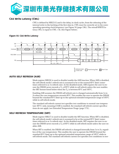
CAS Write Latency (CWL)CWL is defined by MR2[5:3] and is the delay, in clock cycles, from the releasing of the internal write to the latching of the first data in. CWL must be correctly set to the corre-sponding operating clock frequency (see Figure 54 (page 136)). The overall WRITE la-tency (WL) is equal to CWL + AL (See Figure below).Figure 55: CAS Write LatencyCKCK#CommandDQDQS, DQS#Don’t CareIndicates break in time scaleTransitioning Data AUTO SELF REFRESH (ASR)Mode register MR2[6] is used to disable/enable the ASR function. When ASR is disabled,the self refresh mode’s refresh rate is assumed to be at the normal 85°C limit (some-times referred to as 1x refresh rate). In the disabled mode, ASR requires the user to en-sure the DRAM never exceeds a T C of 85°C while in self refresh unless the user enables the SRT feature listed below when the T C is between 85°C and 105°C.Enabling ASR assumes the DRAM self refresh rate is changed automatically from 1x to 2x when the case temperature exceeds 85°C. This enables the user to operate the DRAM beyond the standard 85°C limit up to the optional extended temperature range of 105°C while in self refresh mode.The standard self refresh current test specifies test conditions to normal case tempera-ture (85°C) only, meaning if ASR is enabled, the standard self refresh current specifica-tions do not apply (see Extended Temperature Usage (page 173)).SELF REFRESH TEMPERATURE (SRT)Mode register MR2[7] is used to disable/enable the SRT function. When SRT is disabled,the self refresh mode’s refresh rate is assumed to be at the normal 85°C limit (some-times referred to as 1x refresh rate). In the disabled mode, SRT requires the user to en-sure the DRAM never exceeds a T C of 85°C while in self refresh mode unless the user en-ables ASR.When SRT is enabled, the DRAM self refresh is changed internally from 1x to 2x, regard-less of the case temperature. This enables the user to operate the DRAM beyond the standard 85°C limit up to the optional extended temperature range of 105°C while in self refresh mode. The standard self refresh current test specifies test conditions to nor-Figure 57: Multipurpose Register (MPR) Block DiagramNotes: 1. A predefined data pattern can be read out of the MPR with an external READ com-mand.2.MR3[2] defines whether the data flow comes from the memory core or the MPR. Whenthe data flow is defined, the MPR contents can be read out continuously with a regularREAD or RDAP command.Table 73: MPR Functional Description of MR3 BitsMPR Functional DescriptionThe MPR JEDEC definition enables either a prime DQ (DQ0 on a x4 and a x8; on a x16,DQ0 = lower byte and DQ8 = upper byte) to output the MPR data with the remainingDQs driven LOW, or for all DQs to output the MPR data . The MPR readout supportsfixed READ burst and READ burst chop (MRS and OTF via A12/BC#) with regular READlatencies and AC timings applicable, provided the DLL is locked as required.MPR addressing for a valid MPR read is as follows:•A[1:0] must be set to 00 as the burst order is fixed per nibble•A2 selects the burst order:–BL8, A2 is set to 0, and the burst order is fixed to 0, 1, 2, 3, 4, 5, 6, 7•For burst chop 4 cases, the burst order is switched on the nibble base along with thefollowing:–A2 = 0; burst order = 0, 1, 2, 3–A2 = 1; burst order = 4, 5, 6, 7•Burst order bit 0 (the first bit) is assigned to LSB, and burst order bit 7 (the last bit) isassigned to MSB•A[9:3] are a “Don’t Care”•A10 is a “Don’t Care”•A11 is a “Don’t Care”•A12: Selects burst chop mode on-the-fly, if enabled within MR0•A13 is a “Don’t Care”•BA[2:0] are a “Don’t Care”MPR Register Address Definitions and Bursting OrderThe MPR currently supports a single data format. This data format is a predefined readpattern for system calibration. The predefined pattern is always a repeating 0–1 bit pat-tern.Examples of the different types of predefined READ pattern bursts are shown in the fol-lowing figures.Table 74: MPR Readouts and Burst Order Bit Mapping功率管等;应用领域:航空航天、船舶、汽车电子、军用计算机、铁路、医疗电子、通信网络、电力工业以及大型工业设备祝您:工作顺利,生活愉快!以深圳市美光存储技术有限公司提供的参数为例,以下为MT41K512M16HA-107_A的详细参数,仅供参考。
MT41K512M8DA-107 IT_P
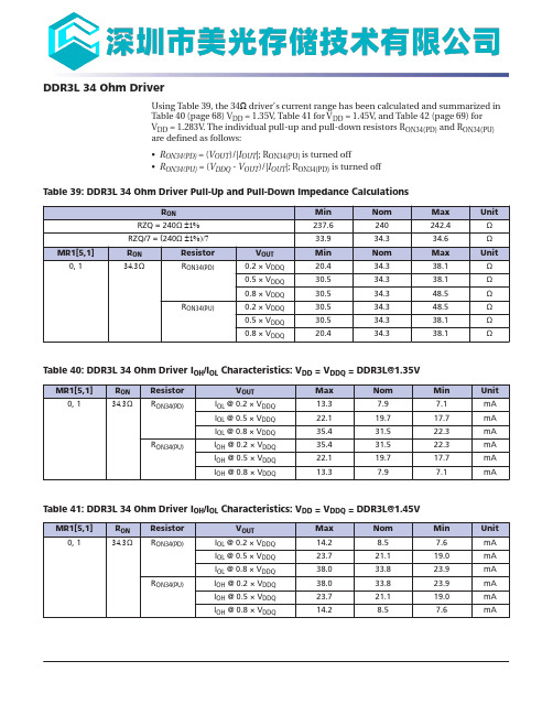
DDR3L 34 Ohm DriverUsing Table 39, the 34ȍ driver’s current range has been calculated and summarized inTable 40 (page 68) V DD = 1.35V, Table 41 for V DD = 1.45V, and Table 42 (page 69) forV DD = 1.283V. The individual pull-up and pull-down resistors R ON34(PD) and R ON34(PU)are defined as follows:•R ON34(PD) = (V OUT)/|I OUT|; R ON34(PU) is turned off•R ON34(PU) = (V DDQ - V OUT)/|I OUT|; R ON34(PD) is turned offTable 39: DDR3L 34 Ohm Driver Pull-Up and Pull-Down Impedance CalculationsTable 40: DDR3L 34 Ohm Driver I OH/I OL Characteristics: V DD = V DDQ = DDR3L@1.35VTable 41: DDR3L 34 Ohm Driver I OH/I OL Characteristics: V DD = V DDQ = DDR3L@1.45VTable 63: DDR3L-1866/2133 Derating Values for t IS/t IH – AC125/DC90-Based (Continued)4Gb: x4, x8, x16 DDR3L SDRAMCommand and Address Setup, Hold, and Derating质量等级领域:宇航级IC、特军级IC、超军级IC、普军级IC、禁运IC、工业级IC,军级二三极管,功率管等;应用领域:航空航天、船舶、汽车电子、军用计算机、铁路、医疗电子、通信网络、电力工业以及大型工业设备祝您:工作顺利,生活愉快!以深圳市美光存储技术有限公司提供的参数为例,以下为MT41K512M8DA-107 IT_P的详细参数,仅供参考Commands – Truth TablesTable 70: Truth Table – CommandNotes: mands are defined by the states of CS#, RAS#, CAS#, WE#, and CKE at the risingedge of the clock. The MSB of BA, RA, and CA are device-, density-, and configuration-dependent.Table 71: Truth Table – CKE。
MEMORY存储芯片MT46V8M16FJ-6中文规格书

fresh mode, the DLL remains disabled even upon exit of SELF REFRESH operation untilit is re-enabled and reset.The DRAM is not tested to check—nor does Micron warrant compliance with—normalmode timings or functionality when the DLL is disabled. An attempt has been made tohave the DRAM operate in the normal mode where reasonably possible when the DLLhas been disabled; however, by industry standard, a few known exceptions are defined:•ODT is not allowed to be used•The output data is no longer edge-aligned to the clock•CL and CWL can only be six clocksWhen the DLL is disabled, timing and functionality can vary from the normal operationspecifications when the DLL is enabled (see DLL Disable Mode (page 125)). Disablingthe DLL also implies the need to change the clock frequency (see Input Clock Frequen-cy Change (page 129)).Output Drive StrengthThe DDR3 SDRAM uses a programmable impedance output buffer. The drive strengthmode register setting is defined by MR1[5, 1]. RZQ/7 (34ȍ [NOM]) is the primary outputdriver impedance setting for DDR3 SDRAM devices. To calibrate the output driver im-pedance, an external precision resistor (RZQ) is connected between the ZQ ball andV SSQ. The value of the resistor must be 240ȍ ±1%.The output impedance is set during initialization. Additional impedance calibration up-dates do not affect device operation, and all data sheet timings and current specifica-tions are met during an update.To meet the 34ȍ specification, the output drive strength must be set to 34ȍ during initi-alization. To obtain a calibrated output driver impedance after power-up, the DDR3SDRAM needs a calibration command that is part of the initialization and reset proce-dure.OUTPUT ENABLE/DISABLEThe OUTPUT ENABLE function is defined by MR1[12], as shown in Figure 56 (page146). When enabled (MR1[12] = 0), all outputs (DQ, DQS, DQS#) function when in thenormal mode of operation. When disabled (MR1[12] = 1), all DDR3 SDRAM outputs(DQ and DQS, DQS#) are tri-stated. The output disable feature is intended to be usedduring I DD characterization of the READ current and during t DQSS margining (writeleveling) only.TDQS EnableTermination data strobe (TDQS) is a feature of the x8 DDR3 SDRAM configuration thatprovides termination resistance (R TT) and may be useful in some system configurations.TDQS is not supported in x4 or x16 configurations. When enabled via the mode register(MR1[11]), the R TT that is applied to DQS and DQS# is also applied to TDQS and TDQS#.In contrast to the RDQS function of DDR2 SDRAM, DDR3’s TDQS provides the termina-tion resistance R TT only. The OUTPUT DATA STROBE function of RDQS is not providedby TDQS; thus, R ON does not apply to TDQS and TDQS#. The TDQS and DM functionsshare the same ball. When the TDQS function is enabled via the mode register, the DMfunction is not supported. When the TDQS function is disabled, the DM function is pro-vided, and the TDQS# ball is not used. The TDQS function is available in the x8 DDR3DLL Disable ModeIf the DLL is disabled by the mode register (MR1[0] can be switched during initializationor later), the DRAM is targeted, but not guaranteed, to operate similarly to the normalmode, with a few notable exceptions:•The DRAM supports only one value of CAS latency (CL = 6) and one value of CASWRITE latency (CWL = 6).•DLL disable mode affects the read data clock-to-data strobe relationship (t DQSCK),but not the read data-to-data strobe relationship (t DQSQ, t QH). Special attention isrequired to line up the read data with the controller time domain when the DLL is dis-abled.•In normal operation (DLL on), t DQSCK starts from the rising clock edge AL + CLcycles after the READ command. In DLL disable mode, t DQSCK starts AL + CL - 1 cy-cles after the READ command. Additionally, with the DLL disabled, the value oft DQSCK could be larger than t CK.The ODT feature (including dynamic ODT) is not supported during DLL disable mode.The ODT resistors must be disabled by continuously registering the ODT ball LOW byprogramming R TT,nom MR1[9, 6, 2] and R TT(WR) MR2[10, 9] to 0 while in the DLL disablemode.Specific steps must be followed to switch between the DLL enable and DLL disablemodes due to a gap in the allowed clock rates between the two modes (t CK [AVG] MAXand t CK [DLL_DIS] MIN, respectively). The only time the clock is allowed to cross thisclock rate gap is during self refresh mode. Thus, the required procedure for switchingfrom the DLL enable mode to the DLL disable mode is to change frequency during selfrefresh:1.Starting from the idle state (all banks are precharged, all timings are fulfilled, ODTis turned off, and R TT,nom and R TT(WR) are High-Z), set MR1[0] to 1 to disable theDLL.2.Enter self refresh mode after t MOD has been satisfied.3.After t CKSRE is satisfied, change the frequency to the desired clock rate.4.Self refresh may be exited when the clock is stable with the new frequency fort CKSRX. After t XS is satisfied, update the mode registers with appropriate values.5.The DRAM will be ready for its next command in the DLL disable mode after thegreater of t MRD or t MOD has been satisfied. A ZQCL command should be issuedwith appropriate timings met.。
MT41K512M8DA-107IT_P
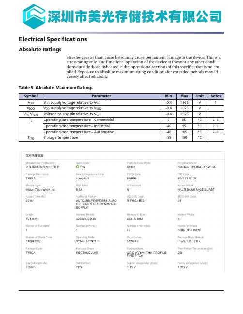
Min –0.4 –0.4 –0.4
0 –40 –40 –55
Max 1.975 1.975 1.975
95 95 105 150
Unit V V V °C °C °C °C
Notes 1
2, 3 2, 3 2, 3
4Gb: x4, x8, x16 DDR3L SDRAM Commands
质量等级领域:宇航级IC、特军级IC、超军级IC、普军级IC、禁运IC、工业级IC,军级二三极 管,功率管等; 应用领域:航空航天、船舶、汽车电子、军用计算机、铁路、医疗电子、通信网络、电力工业以 及大型工业设备 祝您:工作顺利,生活愉快! 以深圳市美光存储技术有限公司提供的参数为例,以下为MT41K512M8DA-107IT_P的详细参数, 仅供参考
RD
H
LH
L
H BA RFU
A12 A10 VL
A[11, 9:0]
CA
RDS4Βιβλιοθήκη HLHLH BA RFU L
L
CA
RDS8
H
LH
L
H BA RFU H L
CA
RDAP
H
LH
L
H BA RFU V H
CA
RDAPS4
H
RDAPS8
H
LH
L
H BA RFU L H
CA
LH
L
H BA RFU H H
CA
WRITE
Table 73: WRITE Command Summary
Function WRITE
WRITE with auto precharge
BL8MRS, BC4MRS BC4OTF BL8OTF BL8MRS, BC4MRS BC4OTF BL8OTF
MEMORY存储芯片MT47J128M8HQ中文规格书
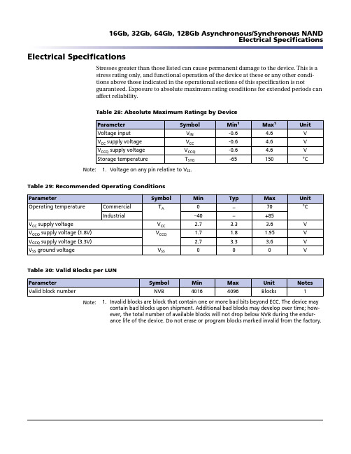
Electrical SpecificationsStresses greater than those listed can cause permanent damage to the device. This is astress rating only, and functional operation of the device at these or any other condi-tions above those indicated in the operational sections of this specification is notguaranteed. Exposure to absolute maximum rating conditions for extended periods canaffect reliability.Table 28: Absolute Maximum Ratings by DeviceNote: 1.Voltage on any pin relative to V SS.Table 29: Recommended Operating ConditionsTable 30: Valid Blocks per LUNNote: 1.Invalid blocks are block that contain one or more bad bits beyond ECC. The device maycontain bad blocks upon shipment. Additional bad blocks may develop over time; how-ever, the total number of available blocks will not drop below NVB during the endur-ance life of the device. Do not erase or program blocks marked invalid from the factory.Activating InterfacesAfter performing the steps under Device Initialization (page 46), the asynchronous inter-face is active for all targets on the device.Each target's interface is independent of other targets, so the host is responsible forchanging the interface for each target.If the host and NAND Flash device, through error, are no longer using the same inter-face, then steps under Activating the Asynchronous Interface are performed to re-synchronize the interfaces.Activating the Asynchronous InterfaceTo activate the asynchronous NAND interface, once the synchronous interface is active,the following steps are repeated for each target:1.The host pulls CE# HIGH, disables its input to CLK, and enables its asynchronousinterface.2.The host pulls CE# LOW and issues the RESET (FFh) command, using an asynchro-nous command cycle.3.R/B# goes LOW for t RST.4.After t ITC, and during t RST, the device enters the asynchronous NAND interface.READ STATUS (70h) and READ STATUS ENHANCED (78h) are the only com-mands that can be issued.5.After t RST, R/B# goes HIGH. Timing mode feature address (01h), subfeature param-eter P1 is set to 00h, indicating that the asynchronous NAND interface is activeand that the device is set to timing mode 0.For further details, see Reset Operations.Activating the Synchronous InterfaceTo activate the synchronous NAND Flash interface, the following steps are repeated foreach target:1.Issue the SET FEATURES (EFh) command.2.Write address 01h, which selects the timing mode.3.Write P1 with 1Xh, where "X" is the timing mode used in the synchronous inter-face (see Configuration Operations).4.Write P2–P4 as 00h-00h-00h.5.R/B# goes LOW for t ITC. The host should pull CE# HIGH. During t ITC, the hostshould not issue any type of command, including status commands, to the NANDFlash device.6.After t ITC, R/B# goes HIGH and the synchronous interface is enabled. Before pull-ing CE# LOW, the host should enable the clock.CHANGE WRITE COLUMN (85h)The CHANGE WRITE COLUMN (85h) command changes the column address of the se-lected cache register and enables data input on the last-selected die (LUN). This com-mand is accepted by the selected die (LUN) when it is ready (RDY = 1; ARDY = 1). It isalso accepted by the selected die (LUN) during cache program operations(RDY = 1; ARDY = 0).Writing 85h to the command register, followed by two column address cycles contain-ing the column address, puts the selected die (LUN) into data input mode. After thesecond address cycle is issued, the host must wait at least t CCS before inputting data.The selected die (LUN) stays in data input mode until another valid command is issued.Though data input mode is enabled, data input from the host is optional. Data inputbegins at the column address specified.The CHANGE WRITE COLUMN (85h) command is allowed after the required addresscycles are specified, but prior to the final command cycle (10h, 11h, 15h) of the follow-ing commands while data input is permitted: PROGRAM PAGE (80h-10h), PROGRAMPAGE MULTI-PLANE (80h-11h), PROGRAM PAGE CACHE (80h-15h), COPYBACK PRO-GRAM (85h-10h), and COPYBACK PROGRAM MULTI-PLANE (85h-11h).In devices that have more than one die (LUN) per target, the CHANGE WRITE COL-UMN (85h) command can be used with other commands that support interleaved die(multi-LUN) operations.Figure 49: CHANGE WRITE COLUMN (85h) OperationCycle type DQ[7:0]RDYAs defined for PAGE As defined for PAGE16Gb, 32Gb, 64Gb, 128Gb Asynchronous/Synchronous NANDColumn Address Operations。
MT41K256M16TW-107 IT_P

Mode RegistersMode registers (MR0–MR3) are used to define various modes of programmable opera-tions of the DDR3 SDRAM. A mode register is programmed via the mode register set (MRS) command during initialization, and it retains the stored information (except for MR0[8], which is self-clearing) until it is reprogrammed, RESET# goes LOW, the device loses power.Contents of a mode register can be altered by re-executing the MRS command. Even if the user wants to modify only a subset of the mode register’s variables, all variables must be programmed when the MRS command is issued. Reprogramming the mode register will not alter the contents of the memory array, provided it is performed cor-rectly.The MRS command can only be issued (or re-issued) when all banks are idle and in the precharged state (t RP is satisfied and no data bursts are in progress). After an MRS com-mand has been issued, two parameters must be satisfied: t MRD and t MOD. The control-ler must wait t MRD before initiating any subsequent MRS commands.Figure 52: MRS to MRS Command Timing (t MRD)CK#CKCommandAddress CKE 3Don’t CareIndicates break in time scale质量等级领域:宇航级IC 、特军级IC 、超军级IC 、普军级IC 、禁运IC 、工业级IC ,军级二三极管,功率管等;应用领域:航空航天、船舶、汽车电子、军用计算机、铁路、医疗电子、通信网络、电力工业以及大型工业设备祝您:工作顺利,生活愉快!以深圳市美光存储技术有限公司提供的参数为例,以下为MT41K256M16TW-107 IT_P的详细参数,仅供参考ing location within the block. The programmed burst length applies to both READ and WRITE bursts.Figure 54: Mode Register 0 (MR0) DefinitionsAddress busMode Register 1 (MR1)The mode register 1 (MR1) controls additional functions and features not available inthe other mode registers: Q OFF (OUTPUT DISABLE), TDQS (for the x8 configurationonly), DLL ENABLE/DLL DISABLE, R TT,nom value (ODT), WRITE LEVELING, POSTEDCAS ADDITIVE latency, and OUTPUT DRIVE STRENGTH. These functions are control-led via the bits shown in Figure 56 (page 146). The MR1 register is programmed via theMRS command and retains the stored information until it is reprogrammed, until RE-SET# goes LOW, or until the device loses power. Reprogramming the MR1 register willnot alter the contents of the memory array, provided it is performed correctly.The MR1 register must be loaded when all banks are idle and no bursts are in progress.The controller must satisfy the specified timing parameters t MRD and t MOD before ini-tiating a subsequent operation.Figure 56: Mode Register 1 (MR1) DefinitionAddress busNotes: 1.MR1[18, 15:13, 10, 8] are reserved for future use and must be programmed to 0.2.During write leveling, if MR1[7] and MR1[12] are 1, then all R TT,nom values are availablefor use.3.During write leveling, if MR1[7] is a 1, but MR1[12] is a 0, then only R TT,nom write valuesare available for use.DLL Enable/DLL DisableThe DLL may be enabled or disabled by programming MR1[0] during the LOAD MODEcommand, as shown in Figure 56 (page 146). The DLL must be enabled for normal oper-ation. DLL enable is required during power-up initialization and upon returning to nor-mal operation after having disabled the DLL for the purpose of debugging or evalua-tion. Enabling the DLL should always be followed by resetting the DLL using the appro-priate LOAD MODE command.If the DLL is enabled prior to entering self refresh mode, the DLL is automatically disa-bled when entering SELF REFRESH operation and is automatically re-enabled and resetupon exit of SELF REFRESH operation. If the DLL is disabled prior to entering self re-fresh mode, the DLL remains disabled even upon exit of SELF REFRESH operation until it is re-enabled and reset.The DRAM is not tested to check—nor does Micron warrant compliance with—normal mode timings or functionality when the DLL is disabled. An attempt has been made to have the DRAM operate in the normal mode where reasonably possible when the DLL has been disabled; however, by industry standard, a few known exceptions are defined:•ODT is not allowed to be used•The output data is no longer edge-aligned to the clock•CL and CWL can only be six clocksWhen the DLL is disabled, timing and functionality can vary from the normal operation specifications when the DLL is enabled (see DLL Disable Mode (page 125)). Disabling the DLL also implies the need to change the clock frequency (see Input Clock Frequen-cy Change (page 129)).SDRAM configuration only and must be disabled via the mode register for the x4 andx16 configurations.On-Die TerminationODT resistance R TT,nom is defined by MR1[9, 6, 2] (see Figure 56 (page 146)). The R TTtermination value applies to the DQ, DM, DQS, DQS#, and TDQS, TDQS# balls. DDR3supports multiple R TT termination values based on RZQ/n where n can be 2, 4, 6, 8, or12 and RZQ is 240ȍ.Unlike DDR2, DDR3 ODT must be turned off prior to reading data out and must remainoff during a READ burst. R TT,nom termination is allowed any time after the DRAM is ini-tialized, calibrated, and not performing read access, or when it is not in self refreshmode. Additionally, write accesses with dynamic ODT (R TT(WR)) enabled temporarily re-places R TT,nom with R TT(WR).The actual effective termination, R TT(EFF), may be different from the R TT targeted due tononlinearity of the termination. For R TT(EFF) values and calculations (see On-Die Termi-nation (ODT) (page 197)).The ODT feature is designed to improve signal integrity of the memory channel by ena-bling the DDR3 SDRAM controller to independently turn on/off ODT for any or all devi-ces. The ODT input control pin is used to determine when R TT is turned on (ODTL on)and off (ODTL off), assuming ODT has been enabled via MR1[9, 6, 2].Timings for ODT are detailed in On-Die Termination (ODT) (page 197).WRITE LEVELINGThe WRITE LEVELING function is enabled by MR1[7], as shown in Figure 56 (page 146).Write leveling is used (during initialization) to deskew the DQS strobe to clock offset asa result of fly-by topology designs. For better signal integrity, DDR3 SDRAM memorymodules adopted fly-by topology for the commands, addresses, control signals, andclocks.The fly-by topology benefits from a reduced number of stubs and their lengths. Howev-er, fly-by topology induces flight time skews between the clock and DQS strobe (andDQ) at each DRAM on the DIMM. Controllers will have a difficult time maintainingt DQSS, t DSS, and t DSH specifications without supporting write leveling in systemswhich use fly-by topology-based modules. Write leveling timing and detailed operationinformation is provided in Write Leveling (page 131).POSTED CAS ADDITIVE LatencyPOSTED CAS ADDITIVE latency (AL) is supported to make the command and data busefficient for sustainable bandwidths in DDR3 SDRAM. MR1[4, 3] define the value of AL,as shown in Figure 57 (page 149). MR1[4, 3] enable the user to program the DDR3SDRAM with AL = 0, CL - 1, or CL - 2.。
MEMORY存储芯片MT45W8MW16BGX-701I中文规格书

Temperature-Controlled Refresh ModeDuring normal operation, temperature-controlled refresh (TCR) mode disabled, the de-vice must have a REFRESH command issued once every t REFI, except for what is al-lowed by posting (see REFRESH Command section). This means a REFRESH command must be issued once every 7.8μs if T C is less than or equal to 85°C, once every 3.9μs if T C is greater than 85°C, once every 1.95μs if T C is greater than 95°C, regardless of whichTemperature Mode is selected (MR4[2]). TCR mode is disabled by setting MR4[3] = 0while TCR mode is enabled by setting MR4[3] = 1. When TCR mode is enabled (MR4[3]= 1), the Temperature Mode must be selected where MR4[2] = 0 enables the NormalTemperature Mode while MR4[2] = 1 enables the Extended Temperature Mode.When TCR mode is enabled, the device will register the externally supplied REFRESHcommand and adjust the internal refresh period to be longer than t REFI of the normal temperature range, when allowed, by skipping REFRESH commands with the propergear ratio. TCR mode has two Temperature Modes to select between the normal tem-perature range and the extended temperature range; the correct Temperature Modemust be selected so the internal control operates correctly. The DRAM must have thecorrect refresh rate applied externally; the internal refresh rate is determined by theDRAM based upon the temperature.Normal Temperature ModeREFRESH commands should be issued to the device with the refresh period equal to t REFI of normal temperature range (-40°C to 85°C). The system must guarantee that the T C does not exceed 85°C when t REFI of the normal temperature range is used. The de-vice may adjust the internal refresh period to be longer than t REFI of the normal tem-perature range by skipping external REFRESH commands with the proper gear ratiowhen T C is below 85°C. The internal refresh period is automatically adjusted inside the DRAM, and the DRAM controller does not need to provide any additional control.Extended Temperature ModeREFRESH commands should be issued to the device with the refresh period equal to t REFI of extended temperature range (85°C to 95°C, or 95°C to 105°C) . The system must guarantee that the T C does not exceed 95°C, or 105°C. Even though the external refresh supports the extended temperature range, the device may adjust its internal refresh pe-riod to be equal to or longer than t REFI of the normal temperature range (-40°C to 85°C)by skipping external REFRESH commands with the proper gear ratio when T C is equal to or below 85°C. The internal refresh period is automatically adjusted inside theDRAM, and the DRAM controller does not need to provide any additional control.Table 49: Normal t REFI Refresh (TCR Enabled)8Gb: x4, x8, x16 DDR4 SDRAM Temperature-Controlled Refresh ModeTable 92: DQ Input Receiver Specifications (Continued)Notes: 1.All Rx mask specifications must be satisfied for each UI. For example, if the minimum in-put pulse width is violated when satisfying TdiVW (MIN), V diVW,max , and minimum slewrate limits, then either TdiVW (MIN) or minimum slew rates would have to be increasedto the point where the minimum input pulse width would no longer be violated.2.Data Rx mask voltage and timing total input valid window where V diVW is centeredaround V CENTDQ,midpoint after V REFDQ training is completed. The data Rx mask is appliedper bit and should include voltage and temperature drift terms. The input buffer designspecification is to achieve at least a BER =1e- 16 when the Rx mask is not violated.3.Defined over the DQ internal V REF range 1.4.Overshoot and undershoot specifications apply.5.DQ input pulse signal swing into the receiver must meet or exceed V IHL(AC)min . V IHL(AC)min is to be achieved on an UI basis when a rising and falling edge occur in the same UI (avalid TdiPW).6.DQ minimum input pulse width defined at the V CENTDQ,midpoint .7.DQS-to-DQ Rx mask offset is skew between DQS and DQ within a nibble (x4) or word(x8, x16 [for x16, the upper and lower bytes are treated as separate x8s]) at the SDRAMballs over process, voltage, and temperature.8.DQ-to-DQ Rx mask offset is skew between DQs within a nibble (x4) or word (x8, x16) atthe SDRAM balls for a given component over process, voltage, and temperature.9.Input slew rate over V diVW mask centered at V CENTDQ,midpoint . Slowest DQ slew rate tofastest DQ slew rate per transition edge must be within 1.7V/ns of each other.10.Input slew rate between V diVW mask edge and V IHL(AC)min points.The following figure shows the Rx mask relationship to the input timing specifications relative to system t DS and t DH. The classical definition for t DS/t DH required a DQ rising8Gb: x4, x8, x16 DDR4 SDRAM Electrical Characteristics – AC and DC Single-Ended Input Measurement LevelsMode Register 4Mode register 4 (MR4) controls various device operating modes as shown in the follow-ing register definition table. Not all settings listed may be available on a die; only set-tings required for speed bin support are available. MR4 is written by issuing the MRScommand while controlling the states of the BG x , BA x , and A x address pins. The map-ping of address pins during the MRS command is shown in the following MR4 Register Definition table.Table 17: Address Pin Mapping Address bus BG1BG0BA1BA0A17RAS _n CAS _n WE _nA13A12A11A10A9A8A7A6A5A4A3A2A1A0Moderegister 2120191817–––13121110987654321Note: 1.RAS_n, CAS_n, and WE_n must be LOW during MODE REGISTER SET (MRS) command.Table 18: MR4 Register Definition8Gb: x4, x8, x16 DDR4 SDRAM Mode Register 4。
MEMORY存储芯片MT45W4MW16PFA-70 L WT中文规格书
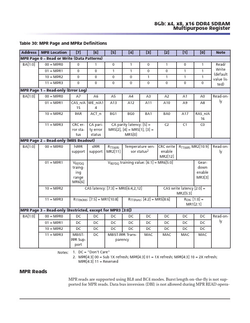
Table 30: MPR Page and MPR x DefinitionsNotes: 1.DC = "Don't Care"2.MPR[4:3] 00 = Sub 1X refresh; MPR[4:3] 01 = 1X refresh; MPR[4:3] 10 = 2X refresh;MPR[4:3] 11 = ReservedMPR ReadsMPR reads are supported using BL8 and BC4 modes. Burst length on-the-fly is not sup-ported for MPR reads. Data bus inversion (DBI) is not allowed during MPR READ opera-8Gb: x4, x8, x16 DDR4 SDRAM Multipurpose Register•Not all features described within this document may be available on the Rev. A (first)version.•Not all specifications listed are finalized industry standards; best conservative esti-mates have been provided when an industry standard has not been finalized.•Although it is implied throughout the specification, the DRAM must be used after V DD has reached the stable power-on level, which is achieved by toggling CKE at least onceevery 8192 × t REFI. However, in the event CKE is fixed HIGH, toggling CS_n at leastonce every 8192 × t REFI is an acceptable alternative. Placing the DRAM into self re-fresh mode also alleviates the need to toggle CKE.•Not all features designated in the data sheet may be supported by earlier die revisionsdue to late definition by JEDEC.•A x16 device's DQ bus is comprised of two bytes. If only one of the bytes needs to beused, use the lower byte for data transfers and terminate the upper byte as noted:–Connect UDQS_t to VDDQ or VSS/ VSSQ via a resistor in the 200വ range.–Connect UDQS_c to the opposite rail via a resistor in the same 200വ range.–Connect UDM to VDDQ via a large (10,000വ) pull-up resistor.–Connect UDBI to VDDQ via a large (10,000വ) pull-up resistor.–Connect DQ [15:8] individually to VDDQ via a large (10,000വ) resistors, or float DQ[15:8] .Definitions of the Device-Pin Signal Level•HIGH: A device pin is driving the logic 1 state.•LOW: A device pin is driving the logic 0 state.•High-Z: A device pin is tri-state.•ODT: A device pin terminates with the ODT setting, which could be terminating or tri-state depending on the mode register setting.Definitions of the Bus Signal Level•HIGH: One device on the bus is HIGH, and all other devices on the bus are either ODTor High-Z. The voltage level on the bus is nominally V DDQ .•LOW: One device on the bus is LOW, and all other devices on the bus are either ODTor High-Z. The voltage level on the bus is nominally V OL(DC) if ODT was enabled, orV SSQ if High-Z.•High-Z: All devices on the bus are High-Z. The voltage level on the bus is undefined asthe bus is floating.•ODT: At least one device on the bus is ODT, and all others are High-Z. The voltage lev-el on the bus is nominally V DDQ .•The specification requires 8,192 refresh commands within 64ms between 0 o C and 85o C. This allows for a t REFI of 7.8125μs (the use of "7.8μs" is truncated from 7.8125μs).The specification also requires 8,192 refresh commands within 32ms between 85 o Cand 95 o C. This allows for a t REFI of 3.90625μs (the use of "3.9μs" is truncated from3.90625μs).8Gb: x4, x8, x16 DDR4 SDRAM General Notes and Description。
MEMORY存储芯片MT45W4MW16PCGA-70WT中文规格书
Per-DRAM AddressabilityDDR4 allows programmability of a single, specific DRAM on a rank. As an example, thisfeature can be used to program different ODT or V REF values on each DRAM on a givenrank. Because per-DRAM addressability (PDA) mode may be used to program optimalV REF for the DRAM, the data set up for first DQ0 transfer or the hold time for the lastDQ0 transfer cannot be guaranteed. The DRAM may sample DQ0 on either the first fall-ing or second rising DQS transfer edge. This supports a common implementation be-tween BC4 and BL8 modes on the DRAM. The DRAM controller is required to drive DQ0to a stable LOW or HIGH state during the length of the data transfer for BC4 and BL8cases. Note, both fixed and on-the-fly (OTF) modes are supported for BC4 and BL8 dur-ing PDA mode.1.Before entering PDA mode, write leveling is required.•BL8 or BC4 may be used.2.Before entering PDA mode, the following MR settings are possible:•R TT(Park) MR5 A[8:6] = Enable•R TT(NOM) MR1 A[10:8] = Enable3.Enable PDA mode using MR3 [4] = 1. (The default programed value of MR3[4] = 0.)4.In PDA mode, all MRS commands are qualified with DQ0. The device capturesDQ0 by using DQS signals. If the value on DQ0 is LOW, the DRAM executes theMRS command. If the value on DQ0 is HIGH, the DRAM ignores the MRS com-mand. The controller can choose to drive all the DQ bits.5.Program the desired DRAM and mode registers using the MRS command andDQ0.6.In PDA mode, only MRS commands are allowed.7.The MODE REGISTER SET command cycle time in PDA mode, AL + CWL + BL/2 -0.5t CK + t MRD_PDA + PL, is required to complete the WRITE operation to themode register and is the minimum time required between two MRS commands.8.Remove the device from PDA mode by setting MR3[4] = 0. (This command re-quires DQ0 = 0.)Note: Removing the device from PDA mode will require programming the entire MR3when the MRS command is issued. This may impact some PDA values programmedwithin a rank as the EXIT command is sent to the rank. To avoid such a case, the PDAenable/disable control bit is located in a mode register that does not have any PDAmode controls.In PDA mode, the device captures DQ0 using DQS signals the same as in a normalWRITE operation; however, dynamic ODT is not supported. Extra care is required forthe ODT setting. If R TT(NOM) MR1 [10:8] = enable, device data termination needs to becontrolled by the ODT pin, and applies the same timing parameters (defined below).8Gb: x4, x8, x16 DDR4 SDRAM Per-DRAM AddressabilityLeakagesTable 81: LeakagesNotes: 1.Input under test 0V < V IN < 1.1V.2.Additional leakage due to weak pull-down.3.V REFCA = V DD /2, V DD at valid level after initialization.4.DQs are disabled.5.ODT is disabled with the ODT input HIGH.V REFCA SupplyV REFCA is to be supplied to the DRAM and equal to V DD /2. The V REFCA is a reference sup-ply input and therefore does not draw biasing current.The DC-tolerance limits and AC-noise limits for the reference voltages V REFCA are illus-trated in the figure below. The figure shows a valid reference voltage V REF(t) as a functionof time (V REF stands for V REFCA ). V REF(DC) is the linear average of V REF(t) over a very longperiod of time (1 second). This average has to meet the MIN/MAX requirements. Fur-thermore, V REF(t) may temporarily deviate from V REF(DC) by no more than ±1% V DD forthe AC-noise limit.Figure 210: V REFDQ Voltage Range8Gb: x4, x8, x16 DDR4 SDRAM Electrical Characteristics – AC and DC Operating ConditionsClock Overshoot and Undershoot SpecificationsTable 112: CK Overshoot and Undershoot/ SpecificationsFigure 230: CK Overshoot and Undershoot DefinitionDD absolute MAX DD absolute MAXSSV o l t s (V )V DD V SS 8Gb: x4, x8, x16 DDR4 SDRAM Electrical Characteristics – Overshoot and Undershoot Specifi-cations。
MEMORY存储芯片MT41J512M8THD-15E中文规格书
easy repair method of the device after placed in the system. One row per bank can berepaired. The repair process is revocable by either doing a reset or power-down or byrewriting a new address in the same bank.WRITE PreambleProgrammable WRITE preamble, t WPRE, can be set to 1t CK or 2t CK via the MR4 register.The 1t CK setting is similar to DDR3. However, when operating in 2t CK WRITE preamblemode, CWL must be programmed to a value at least 1 clock greater than the lowest CWLsetting supported in the applicable t CK range.When operating in 2t CK WRITE preamble mode, CWL must be programmed to a valueat least 1 clock greater than the lowest CWL setting supported in the applicable t CKrange. Some even settings will require addition of 2 clocks. If the alternate longer CWLwas used, the additional clocks will not be required.READ PreambleProgrammable READ preamble t RPRE can be set to 1t CK or 2t CK via the MR4 register.Both the 1t CK and 2t CK DDR4 preamble settings are different from that defined for theDDR3 SDRAM. Both DDR4 READ preamble settings may require the memory controllerto train (or read level) its data strobe receivers using the READ preamble training. READ Preamble TrainingProgrammable READ preamble training can be set to 1t CK or 2t CK. This mode can beused by the memory controller to train or READ level its data strobe receivers. Temperature-Controlled RefreshWhen temperature-controlled refresh mode is enabled, the device may adjust the inter-nal refresh period to be longer than t REFI of the normal temperature range by skippingexternal REFRESH commands with the proper gear ratio. For example, the DRAM tem-perature sensor detected less than 45°C. Normal temperature mode covers the range of–40°C to 85°C, while the extended temperature range covers –40°C to 125°C. Command Address LatencyCOMMAND ADDRESS LATENCY (CAL) is a power savings feature and can be enabledor disabled via the MRS setting. CAL is defined as the delay in clock cycles (t CAL) be-tween a CS_n registered LOW and its corresponding registered command and address.The value of CAL (in clocks) must be programmed into the mode register and is basedon the roundup (in clocks) of [t CK(ns)/t CAL(ns)].Internal V REF MonitorThe device generates its own internal V REFDQ. This mode may be enabled during V REFDQtraining, and when enabled, V REF,time-short and V REF,time-long need to be increased by 10nsif DQ0, DQ1, DQ2, or DQ3 have 0pF loading. An additional 15ns per pF of loading is alsoneeded.Figure 194: Nonconsecutive WRITE (BL8/BC4-OTF) with 1t CK Preamble and Write CRC in Same or Dif-ferent Bank GroupNotes: 1.BL8/BC4-OTF, AL = 0, CWL = 9, Preamble = 1t CK, t CCD_S/L = 6t CK.2.DI n (or b) = data-in from column n (or column b).3.DES commands are shown for ease of illustration; other commands may be valid atthese times.4.BL8 setting activated by either MR0[1:0] = 00 or MR0[1:0] = 01 and A12 = 1 duringWRITE commands at T0 and T6.5.BC4 setting activated by MR0[1:0] = 01 and A12 = 0 during WRITE commands at T0 andT6.6.CA parity = Disable, CS to CA latency = Disable, Read DBI = Disable, Write CRC = Enable,DM = Disable.7.The write recovery time (t WR) and write timing parameter (t WTR) are referenced fromthe first rising clock edge after the last write data shown at T19.。
MEMORY存储芯片MT41K256M32SLD-125中文规格书
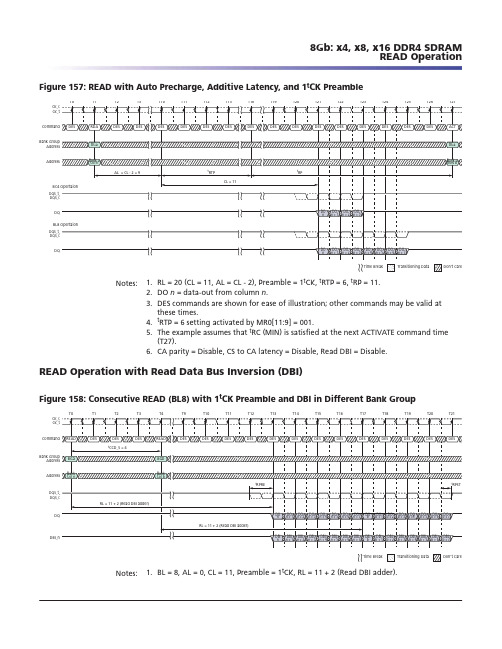
Figure 157: READ with Auto Precharge, Additive Latency, and 1t CK PreambleCommand DQCK_t CK_cDQS_t,DQS_cBank GroupAddress DQ DQS_t,DQS_c Address Notes: 1.RL = 20 (CL = 11, AL = CL - 2), Preamble = 1t CK, t RTP = 6, t RP = 11.2.DO n = data-out from column n .3.DES commands are shown for ease of illustration; other commands may be valid atthese times.4.t RTP = 6 setting activated by MR0[11:9] = 001.5.The example assumes that t RC (MIN) is satisfied at the next ACTIVATE command time(T27).6.CA parity = Disable, CS to CA latency = Disable, Read DBI = Disable.READ Operation with Read Data Bus Inversion (DBI)Figure 158: Consecutive READ (BL8) with 1t CK Preamble and DBI in Different Bank GroupT0T16T1T2T3T4T9T10T11T12T13T14T15Command DQCK_t CK_cDQS_t,DQS_cT21T17T18T19T20Bank GroupAddress Address DBI_n Notes: 1.BL = 8, AL = 0, CL = 11, Preamble = 1t CK, RL = 11 + 2 (Read DBI adder).8Gb: x4, x8, x16 DDR4 SDRAM READ OperationTable 154: I DD , I PP , and I DDQ Current Limits; Die Rev. H (0° ื T C ื 85°C) (Continued)Notes: 1.Applicable for MR2 settings A7 = 0 and A6 = 0; manual mode with normal temperaturerange of operation (0–85°C).2.Applicable for MR2 settings A7 = 1 and A6 = 0; manual mode with extended tempera-ture range of operation (0–95°C).3.Applicable for MR2 settings A7 = 0 and A6 = 1; manual mode with reduced temperature range of operation (0–45°C).4.I DD6E , I DD6R , I DD6A values are verified by design and characterization, and may not be subject to production test.5.When additive latency is enabled for I DD0, current changes by approximately 0%.6.When additive latency is enabled for I DD1, current changes by approximately +5%(x4/x8),+4%(x16).7.When additive latency is enabled for I DD2N , current changes by approximately 0%.8Gb: x4, x8, x16 DDR4 SDRAM Current Specifications – Limits。
MT4错误代码最完整汇总
请问MT4 EA不能开单,日志显示“OrderSend error 130”是什么意思最好能直接给我一个能用的ORDERSEND的代码,希望能根据相应条件,每个货币对都能开单而且只开一单。
举报违规检举侵权投诉|2013-08-23 13:19 提问者采纳百度啊,大哥。
也有MT4错误代码表的。
ERR_INVALID_STOPS,检查你的止损价位,是不是太近、甚至设反了。
======================================================================MT4错误代码最完整汇总(2011-05-16 09:44:02)转载▼标签:杂谈分类:外汇MT4 的错误代码是存放在MetaEditor的libraries文件夹下 stdlib.mq4或stderror.mq4文件中但是内容都是英文,我将这部分的翻译转过来,以供参考case 1: error_string="no error"; 没有错误返回。
;case 2: error_string="common error"; 没有错误返回但结果不明;case 3: error_string="invalid trade parameters"; 一般错误;case 4: error_string="trade server is busy";无效交易参量;case 5: error_string="old version of the client terminal";交易服务器繁忙; case 6: error_string="no connection with trade server";客户终端旧版本; case 7: error_string="not enough rights";没有连接服务器;case 8: error_string="too frequent requests";没有权限;case 9: error_string="malfunctional trade operation (never returned error)";请求过于频繁;case 64: error_string="account disabled"; 交易运行故障;case 65: error_string="invalid account";账户禁止;case 128: error_string="trade timeout";无效超时;case 129: error_string="invalid price"; 无效价格;case 130: error_string="invalid stops";无效停止;case 131: error_string="invalid trade volume";无效交易量;case 132: error_string="market is closed";市场关闭;case 133: error_string="trade is disabled";交易被禁止;case 134: error_string="not enough money";资金不足;case 135: error_string="price changed";价格改变;case 136: error_string="off quotes"; 开价;case 137: error_string="broker is busy (never returned error)";经纪繁忙; case 138: error_string="requote";重新开价;case 139: error_string="order is locked";定单被锁定;case 140: error_string="long positions only allowed";只允许看涨仓位;case 141: error_string="too many requests";过多请求;case 145: error_string="modification denied because order too close to market";因为过于接近市场,修改否定;case 146: error_string="trade context is busy";交易文本已满;case 147: error_string="expirations are denied by broker";时间周期被经纪否定;case 148: error_string="amount of open and pending orders has reached the limit";开单和挂单总数已被经纪限定;case 149: error_string="hedging is prohibited";当对冲备拒绝时,打开相对于现有的一个单置;case 150: error_string="prohibited by FIFO rules";把为反FIFO规定的单子平掉;以下是mql4的错误代码case 4000: error_string="no error (never generated code)"; 没有错误;case 4001: error_string="wrong function pointer"; 错误函数指示;case 4002: error_string="array index is out of range";数组索引超出范围; case 4003: error_string="no memory for function call stack"; 对于调用堆栈储存器函数没有足够内存;case 4004: error_string="recursive stack overflow"; 循环堆栈储存器溢出; case 4005: error_string="not enough stack for parameter";对于堆栈储存器参量没有内存;case 4006: error_string="no memory for parameter string";对于字行参量没有足够内存;case 4007: error_string="no memory for temp string";对于字行没有足够内存; case 4008: error_string="not initialized string";没有初始字行;case 4009: error_string="not initialized string in array";在数组中没有初始字串符;case 4010: error_string="no memory for array\' string";对于数组没有内存; case 4011: error_string="too long string"; 字行过长;case 4012: error_string="remainder from zero divide"; 余数划分为零;case 4013: error_string="zero divide"; 零划分;case 4014: error_string="unknown command";不明命令;case 4015: error_string="wrong jump (never generated error)";错误转换(没有常规错误);case 4016: error_string="not initialized array";没有初始数组;case 4017: error_string="dll calls are not allowed";禁止调用DLL; //出现这个异常在导入时候运行动态调用dll即可case 4018: error_string="cannot load library"; 数据库不能下载;case 4019: error_string="cannot call function"; 不能调用函数;case 4020: error_string="expert function calls are not allowed";禁止调用智能交易函数;case 4021: error_string="not enough memory for temp string returned from function"; 对于来自函数的字行没有足够内存;case 4022: error_string="system is busy (never generated error)";系统繁忙(没有常规错误);case 4050: error_string="invalid function parameters count"; 无效计数参量函数;case 4051: error_string="invalid function parameter value"; 无效参量值函数; case 4052: error_string="string function internal error";字行函数内部错误; case 4053: error_string="some array error"; 一些数组错误;case 4054: error_string="incorrect series array using";应用不正确数组;case 4055: error_string="custom indicator error"; 自定义指标错误;case 4056: error_string="arrays are incompatible"; 不协调数组;case 4057: error_string="global variables processing error";整体变量过程错误;case 4058: error_string="global variable not found"; 整体变量未找到;case 4059: error_string="function is not allowed in testing mode";测试模式函数禁止;case 4060: error_string="function is not confirmed";没有确认函数;case 4061: error_string="send mail error"; 发送邮件错误;case 4062: error_string="string parameter expected"; 字行预计参量;case 4063: error_string="integer parameter expected"; 整数预计参量;case 4064: error_string="double parameter expected"; 双预计参量;case 4065: error_string="array as parameter expected"; 数组作为预计参量; case 4066: error_string="requested history data in update state"; 刷新状态请求历史数据;case 4067: error_string="ERR_TRADE_ERROR";交易函数错误;case 4099: error_string="end of file ERR_END_OF_FILE"; 文件结束;case 4100: error_string="some file error"; 一些文件错误;case 4101: error_string="wrong file name";错误文件名称case 4102: error_string="too many opened files";打开文件过多;case 4103: error_string="cannot open file"不能打开文件;case 4104: error_string="incompatible access to a file"不协调文件;case 4105: error_string="no order selected"没有选择定单;case 4106: error_string="unknown symbol";不明货币对;case 4107: error_string="invalid price parameter for trade function"; 无效价格;case 4108: error_string="invalid ticket"; 无效定单编码;case 4109: error_string="trade is not allowed in the expert properties"; 不允许交易;case 4110: error_string="longs are not allowed in the expert properties"; 不允许长期;case 4111: error_string="shorts are not allowed in the expert properties"; 不允许短期;case 4200: error_string="object is already exist"; 定单已经存在;case 4201: error_string="unknown object property"; 不明定单属性;case 4202: error_string="object is not exist"; 定单不存在;case 4203: error_string="unknown object type"; 不明定单类型;case 4204: error_string="no object name";没有定单名称;case 4205: error_string="object coordinates error"; 定单坐标错误;case 4206: error_string="no specified subwindow"; 没有指定子窗口;MT4 的错误代码是存放在MetaEditor的libraries文件夹下 stdlib.mq4或stderror.mq4文件中但是内容都是英文,我将这部分的翻译转过来,以供参考case 1: error_string="no error"; 没有错误返回。
- 1、下载文档前请自行甄别文档内容的完整性,平台不提供额外的编辑、内容补充、找答案等附加服务。
- 2、"仅部分预览"的文档,不可在线预览部分如存在完整性等问题,可反馈申请退款(可完整预览的文档不适用该条件!)。
- 3、如文档侵犯您的权益,请联系客服反馈,我们会尽快为您处理(人工客服工作时间:9:00-18:30)。
DDR3L SDRAM
MT41K1G4 – 128 Meg x 4 x 8 banks
MT41K512M8 – 64 Meg x 8 x 8 banks MT41K256M16 – 32 Meg x 16 x 8 banks
Description
DDR3L SDRAM (1.35V) is a low voltage version of the DDR3 (1.5V) SDRAM. Refer to DDR3 (1.5V) SDRAM (Die Rev :E) data sheet specifications when running in 1.5V compatible mode.
Features
•V DD = V DDQ = 1.35V (1.283–1.45V)
•Backward compatible to V DD = V DDQ = 1.5V ±0.075V –Supports DDR3L devices to be backward com-patible in 1.5V applications
•Differential bidirectional data strobe
•8n-bit prefetch architecture
•Differential clock inputs (CK, CK#)
•8 internal banks
•Nominal and dynamic on-die termination (ODT) for data, strobe, and mask signals •Programmable CAS (READ) latency (CL)•Programmable posted CAS additive latency (AL)•Programmable CAS (WRITE) latency (CWL)•Fixed burst length (BL) of 8 and burst chop (BC) of 4 (via the mode register set [MRS])
•Selectable BC4 or BL8 on-the-fly (OTF)
•Self refresh mode
•T C of 105°C
–64ms, 8192-cycle refresh up to 85°C
–32ms, 8192-cycle refresh at >85°C to 95°C
–16ms, 8192-cycle refresh at >95°C to 105°C •Self refresh temperature (SRT)
•Automatic self refresh (ASR)
•Write leveling
•Multipurpose register
•Output driver calibration
Options Marking •Configuration
– 1 Gig x 41G4
–512 Meg x 8512M8–256 Meg x 16256M16•FBGA package (Pb-free) – x4, x8
–78-ball (9mm x 10.5mm) Rev. E RH
–78-ball (7.5mm x 10.6mm) Rev. N RG
–78-ball (8mm x 10.5mm) Rev. P DA •FBGA package (Pb-free) – x16
–96-ball (9mm x 14mm) Rev. E HA
–96-ball (7.5mm x 13.5mm) Rev. N LY
–96-ball (8mm x 14mm) Rev. P TW •Timing – cycle time
–938ps @ CL = 14 (DDR3-2133)-093
– 1.07ns @ CL = 13 (DDR3-1866)-107
– 1.25ns @ CL = 11 (DDR3-1600)-125•Operating temperature
–Commercial (0°C T C +95°C)None
–Industrial (–40°C T C +95°C)IT
–Automotive (–40°C T C +105°C)AT •Revision:E/:N/:P
Table 1: Key Timing Parameters
Notes: 1.Backward compatible to 1600, CL = 11 (-125).
2.Backward compatible to 1866, CL = 13 (-107).
Table 2: Addressing
Figure 1: DDR3L Part Numbers
([DPSOH 3DUW 1XPEHU 07 . 0 '$ 3
Note:
1.Not all options listed can be combined to define an offered product. Use the part catalog search on
for available offerings.
4Gb: x4, x8, x16 DDR3L SDRAM
Description
质量等级领域:宇航级IC、特军级IC、超军级IC、普军级IC、禁运IC、工业级IC,军级二三极管,功率管等;
应用领域:航空航天、船舶、汽车电子、军用计算机、铁路、医疗电子、通信网络、电力工业以及大型工业设备
祝您:工作顺利,生活愉快!
以深圳市美光存储技术有限公司提供的参数为例,以下为MT41K512M8DA-107_P的详细参数,仅供参考
DDR3L 1.35V Slew Rate Definitions for Differential Input Signals
Input slew rate for differential signals (CK, CK# and DQS, DQS#) are defined and meas-
ured, as shown in Table 31 and Figure 22. The nominal slew rate for a rising signal is
defined as the slew rate between V IL,diff,max and V IH,diff,min. The nominal slew rate for a
falling signal is defined as the slew rate between V IH,diff,min and V IL,diff,max.
Table 31: DDR3L 1.35V Differential Input Slew Rate Definition
Output Driver Impedance
The output driver impedance is selected by MR1[5,1] during initialization. The selected value is able to maintain the tight tolerances specified if proper ZQ calibration is per-formed. Output specifications refer to the default output driver unless specifically sta-ted otherwise. A functional representation of the output buffer is shown below. The out-put driver impedance R ON is defined by the value of the external reference resistor RZQ as follows:
•R ON,x = RZQ /y (with RZQ = 240ȍ ±1%; x = 34ȍ or 40ȍ with y = 7 or 6, respectively)The individual pull-up and pull-down resistors R ON(PU) and R ON(PD) are defined as fol-lows:
•R ON(PU) = (V DDQ - V OUT )/|I OUT |, when R ON(PD) is turned off •R ON(PD) = (V OUT )/|I OUT |, when R ON(PU) is turned off
Figure 28: Output Driver
Output driver
Chip in drive mode V DDQ
V SSQ
V OUT DQ
4Gb: x4, x8, x16 DDR3L SDRAM
Output Driver Impedance。