A158S13中文资料
EN150853ISO9013 演示文稿

■ 3.9 顶部边缘溶解r 测量上部边缘切割形成特性 注释:上部边缘可以是陡沿熔化边缘或者突出切削
边缘 ■ 3.10 刨削槽 对不规则的宽度深度以及形状进行冲刷或掏槽最好
是沿着切削厚度方 向这样可以其他形式的切削面
A 切削方向 B 进给方向
■ 5.2.3有关焊接性能等级的螺柱焊接缺陷质量等 级
■ 螺柱焊接的接头只允许采用焊接性能等级CP C3 和 CP D,并应满足EN ISO 14555 的要求。
■ 如果不能达到焊接性能等级,设计人员应当降 低应力等级或改变设计。
■ 5.2.4 电阻点焊、多点凸焊和电阻缝焊的质 量要求
■ 电阻点焊、多点凸焊和电阻缝焊的质量要求在 表 2 中定义。有关表面质量,适用表T.3。
■ 如果合同中有要求,设计人员对每个焊缝安全等级的验 收应经过客户和/或国家安全部门的批准。
■ 为了确定安全等级,还应考虑到附录G。
■ 表 3焊接性能等级与检查等级之间的对应关系
焊接性能等级
检查等级最低要求
CPA
CT 1
CPB
CT 2
CPC1
CT 2
CPC2
CT 3
CPC3
CT4
■ 4.8 应力等级、安全等级、焊接性能等级、缺陷 质量等级、检查等级和试验之间的关系
a 加工件厚度 b 切割厚度(可能性最大) c 榫头深度/切割厚度可能性最大 d 切割厚度第二可能性 e 切割长度
3.2.3 切削类型
1 垂直切割 2 倾斜式切割 3 倾斜式切割2 次切割
■ 3.3切削速度 ■ 是指在工具例如火焰喷管与工件之间的相对速度 ■ 3.4 切缝宽度 ■ 由切割射流产生的切割顶边缘或存在的顶边缘融
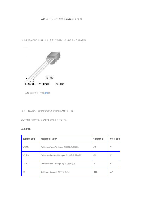
A1015中文资料参数
mA
IB
Base Current基极电流
-50
mA
PC
Collector Power Dissipation耗散功率
400
mW
TJ
Junction Temperature结温
125
℃
TSTG
Storage Temperature贮藏温度
-65 ~ 150
℃
电参数:
Symbol符号
Parameter参数
Value数值
Units单位
Vቤተ መጻሕፍቲ ባይዱBO
Collector-Base Voltage集电极-基极电压
-60
V
VCEO
Collector-Emitter Voltage集电极-射极电压
-50
V
VEBO
Emitter-Base Voltage射极-基极电压
-5
V
IC
Collector Current集电极电流
Test Condition测试条件
Min最小
Typ平均
Max最大
Units单位
BVCBO
Collector-Base Breakdown Voltage集电极-基极击穿电压
IC= -100μA, IE=0
-50
-
-
V
BVCEO
Collector-Emitter Breakdown Voltage集电极-发射极击穿电压
VCB=10V, IE=0, f=1MHz
-
4.0
7.0
pF
NF
Noise Figure噪声系数
VCE=6V, IC=0.1mA RS=10kΩ, f=1Hz
IT-158 datasheet-201409

Multifunctional Filled Epoxy Resin and Phenolic-Cured Lead Free Laminate & Prepreg
IT-158 is a medium Tg (>150℃ by DSC) multifunctional filled epoxy with high thermal reliability and CAF resistance. It’s suitable for industrial PCB, automobile and can pass 260℃ Lead free assembly.
Key Features ===============================
Advanced Resin Technology
Industrial standard material with medium Tg (150℃ by DSC) multifunctional filled epoxy resin and excellent thermal reliability.
1. After Thermal Stress 2. At 125°C [257 F] 3. After Process Solutions
0.88 (5.0)
1.58 (9.0) 1.31 (7.5) 1.14 (6.5)
0.70 (4.00)
0.80 (4.57) 0.70 (4.00) 0.55 (3.14)
Thickness<0.50 mm
Thickness≧0.50 mm
Property
Typical Value
[0.0197 in] Spec
SA158中文资料

1)Max. temperature of the terminals T = 100/C – Max. Temperatur der Anschlüsse T = 100/CFast SwitchingSchnelle Si-GleichrichterSurface Mount Si-Rectifiersfür die OberflächenmontageNominal current – Nennstrom 1 ARepetitive peak reverse voltage 50…1000 V Periodische Spitzensperrspannung Plastic case MELFDO-213ABKunststoffgehäuse MELF Weight approx. – Gewicht ca.0.12 gPlastic material has UL classification 94V-0Gehäusematerial UL94V-0 klassifiziertDimensions / Maße in mmStandard packaging taped and reeled see page 18Standard Lieferform gegurtet auf Rolle siehe Seite 18Maximum ratings GrenzwerteType Typ Repetitive peak reverse voltage Periodische SpitzensperrspannungV RRM [V]Surge peak reverse voltage StoßspitzensperrspannungV RSM [V]SA 1545050SA 155100100SA 156200200SA 157400400SA 158600600SA 159800800SA 16010001000Max. average forward rectified current, R-load T T = 100/C I FAV 1 A Dauergrenzstrom in Einwegschaltung mit R-Last Repetitive peak forward current f > 15 Hz I FRM 10 A 1)Periodischer SpitzenstromPeak forward surge current, 50 Hz half sine-wave T A = 25/C I FSM 35 A Stoßstrom für eine 50 Hz Sinus-Halbwelle Rating for fusing, t < 10 ms T A = 25/Ci 2t6 A 2sGrenzlastintegral, t < 10 ms1)Mounted on P.C. board with 25 mm 2 copper pads at each terminalMontage auf Leiterplatte mit 25 mm 2 Kupferbelag (Lötpad) an jedem AnschlußOperating junction temperature – Sperrschichttemperatur T j – 50...+175/C Storage temperature – LagerungstemperaturT S– 50...+175/CCharacteristicsKennwerteForward voltage – Durchlaßspannung T j = 25/C I F = 1 A V F < 1.3 V Leakage current – Sperrstrom T j = 25/C V R = V RRM I R < 5 :A T j = 100/CV R = V RRMI R < 100 :A Reverse recovery time I F = 0.5 A through/über t rr < 300 ns SperrverzugI R = 1 A to/auf I R = 0.25AThermal resistance junction to ambient airR thA < 45 K/W 1)Wärmewiderstand Sperrschicht – umgebende Luft Thermal resistance junction to terminalR thT< 15 K/WWärmewiderstand Sperrschicht – Kontaktfläche。
2SA2013中文资料(ONSEMI)中文数据手册「EasyDatasheet - 矽搜」

Unit µA µA MHz
200 (360)400
本文描述或包含没有规范,能够处理应用需要极高的可靠性,如生命支持系统,飞机的控制系统或其他应用程序的 故障可合理预期会导致严重的身体任何及所有SANYO产品和/或财产损失.使用任何SANYO产品中,在此类应用中描述或包 含前与您的SANYO代表就近请教.
芯片中文手册,看全文,戳
订购数量: ENN6307B
2SA2013 / 2SC5566
2SA2013 / 2SC5566 DC / DC转换器应用
应用
•
PNP / NPN外延平面硅晶体管
继电器驱动器,灯驱动器,电机驱动器,闪存.
特征
• • • • • •
采用FBET和MBIT过程. 高电流容量. 低集电极 - 发射极饱和电压. 高速切换. 超小型封装facilitales 小型化的终端产品. 高允许功耗.
4
IC - VCE
mA 70 mA 80 90mA 100mA A 60m 50mA 40mA 30mA 20mA 10mA
--3
3
--2 集电极电流,IC - 一个 --1
2
--10mA
集电极电流,IC - 一个 1
0
IB=0mA
0 --0.4 --0.8 --1.2 集电极 - 发射极电压VCE - V --1.6 --2.0 IT00152
--25° C
5°C Ta=7 25°C
饱和电压 )° -C 毫伏 10 ,VCE(SAT --25 7 5 3 2 1.0 0.01 2 3 5 7 0.1
°C a=75 T 25°C
2 3
5 7 1.0
2
3
集电极电流,IC - 一个 10000 7 5 3 2 1000 7 5 集电极 - 发射极 3 2 100 ,VCE(SAT) - 毫伏 饱和电压 7 ° Ta=75 C 5
铝硅焊丝型号

铝硅焊丝型号
AlSi4,5是一种低熔点的耐高温的铝硅焊丝,具有优异的焊接性能,可以用于正火工艺共轨式焊接和表面焊接,用于焊接铝合金、镁合金、铁、碳钢和钛合金等金属材料。
2、AlSi12:
AlSi12也是一种耐高温的铝硅焊丝,有良好的焊接性能和耐腐蚀性。
它适用于焊接各种铝合金、钢、铁、镁合金等金属材料。
3、AlSi10:
AlSi10是一种高熔点的铝硅焊丝,具有良好的焊接性能和耐腐蚀性,可用于焊接各种铝合金、钢、铁、镁合金等金属材料。
4、AlSi15:
AlSi15是一种高熔点的铝硅焊丝,具有良好的焊接性能和较高的耐热性。
用于焊接各种铝合金、钢、铁、镁合金等金属材料,特别适用于高温焊接。
5、AlSi20:
AlSi20是一种高熔点铝硅焊丝,具有良好的焊接性能和较高的耐热性。
用于焊接碳钢、低合金钢、易焊性铝合金等金属材料。
6、AlSi25:
AlSi25是一种高熔点铝硅焊丝,具有良好的焊接性能和较高的耐热性。
用于焊接碳钢、低合金钢、易焊性铝合金等金属材料,特别适用于高温焊接。
- 1 -。
S13油浸式变压器技术投标文件

4 标准技术参数技术参数特性表是国家电网公司对采购设备的基础技术参数要求,在招投标过程中,投标人应该依据招标文件,对技术参数特性表中标准参数值进行响应。
10kV宜采用油浸式、全密封、低损耗三相油浸式变压器;三相变接线组别Dyn11。
表1 技术参数特性表附表1.1 S13型性能参数表附表2 噪声水平5 组件材料配置表组件材料配置见表2;包括元件名称、规格形式参数、单位、数量等信息,具体内容和格式根据招标项目情况进行编制。
表2项目货物组件材料配置表6 使用环境条件表10kV三相油浸式变压器使用环境条件见表3。
特殊环境要求根据项目情况进行编制。
表3 使用环境条件表4 标准技术参数技术参数特性表是国家电网公司对采购设备的基础技术参数要求,在招投标过程中,投标人应该依据招标文件,对技术参数特性表中标准参数值进行响应。
10kV宜采用油浸式、全密封、低损耗三相油浸式变压器;三相变接线组别Dyn11。
表1 技术参数特性表附表1.1 S13型性能参数表附表2 噪声水平5 组件材料配置表组件材料配置见表2;包括元件名称、规格形式参数、单位、数量等信息,具体内容和格式根据招标项目情况进行编制。
表2项目货物组件材料配置表表2项目货物组件材料配置表表2项目货物组件材料配置表6 使用环境条件表10kV三相油浸式变压器使用环境条件见表3。
特殊环境要求根据项目情况进行编制。
表3 使用环境条件表4 标准技术参数技术参数特性表是国家电网公司对采购设备的基础技术参数要求,在招投标过程中,投标人应该依据招标文件,对技术参数特性表中标准参数值进行响应。
10kV宜采用油浸式、全密封、低损耗三相油浸式变压器;三相变接线组别Dyn11。
表1 技术参数特性表附表1.1 S13型性能参数表附表2 噪声水平5 组件材料配置表组件材料配置见表2;包括元件名称、规格形式参数、单位、数量等信息,具体内容和格式根据招标项目情况进行编制。
表2项目货物组件材料配置表6 使用环境条件表10kV三相油浸式变压器使用环境条件见表3。
SCDS158A 型号电路芯片说明书

SN74CB3T338310ĆBIT FET BUSĆEXCHANGE SWITCH2.5ĆV/3.3ĆV LOWĆVOLTAGE BUS SWITCH WITH 5ĆVĆTOLERANT LEVEL SHIFTERSCDS158A − OCTOBER 2003 − REVISED DECEMBER 20041POST OFFICE BOX 655303 •DALLAS, TEXAS 75265D Output Voltage Translation Tracks V CCD Supports Mixed-Mode Signal Operation OnAll Data I/O Ports− 5-V Input Down To 3.3-V Output Level Shift With 3.3-V V CC− 5-V/3.3-V Input Down To 2.5-V Output Level Shift With 2.5-V V CCD 5-V-Tolerant I/Os With Device Powered Up or Powered DownD Bidirectional Data Flow, With Near-Zero Propagation DelayD Low ON-State Resistance (r on )Characteristics (r on = 5 Ω Typical)D Low Input/Output Capacitance Minimizes Loading (C io(OFF) = 8 pF Typical)D Data and Control Inputs Provide Undershoot Clamp Diodes DLow Power Consumption (I CC = 20 µA Max)D V CC Operating Range From 2.3 V to 3.6 V D Data I/Os Support 0- to 5-V Signaling Levels (0.8 V, 1.2 V, 1.5 V, 1.8 V, 2.5 V, 3.3 V,5 V)D Control Inputs Can Be Driven by TTL or 5-V/3.3-V CMOS OutputsD I off Supports Partial-Power-Down Mode OperationD Latch-Up Performance Exceeds 250 mA Per JESD 17DESD Performance Tested Per JESD 22− 2000-V Human-Body Model (A114-B, Class II)− 1000-V Charged-Device Model (C101)D Supports Digital Applications: Level Translation, Memory Interleaving, Bus IsolationDIdeal for Low-Power Portable EquipmentDBQ, DGV, DW, OR PW PACKAGE(TOP VIEW)BE 1B11A11A21B22B12A12A22B23B13A1GNDV CC 5B25A25A15B14B24A24A14B13B23A2BX123456789101112242322212019181716151413description/ordering informationORDERING INFORMATIONT APACKAGE †ORDERABLE PART NUMBER TOP-SIDE MARKING Tube SN74CB3T3383DW SOIC − DWTape and reel SN74CB3T3383DWR CB3T3383SSOP (QSOP) − DBQ Tape and reel SN74CB3T3383DBQR CB3T3383−40°C to 85°CTube SN74CB3T3383PW TSSOP − PW Tape and reel SN74CB3T3383PWR KS383TVSOP − DGVTape and reelSN74CB3T3383DGVRKS383†Package drawings, standard packing quantities, thermal data, symbolization, and PCB design guidelines are available at /sc/package.Copyright 2004, Texas Instruments IncorporatedPlease be aware that an important notice concerning availability, standard warranty, and use in critical applications of Texas Instruments semiconductor products and disclaimers thereto appears at the end of this data sheet.PRODUCTION DATA information is current as of publication date.Products conform to specifications per the terms of Texas Instruments standard warranty. Production processing does not necessarily include testing of all parameters.SN74CB3T338310ĆBIT FET BUSĆEXCHANGE SWITCH2.5ĆV/3.3ĆV LOWĆVOLTAGE BUS SWITCH WITH 5ĆVĆTOLERANT LEVEL SHIFTERSCDS158A − OCTOBER 2003 − REVISED DECEMBER 20042POST OFFICE BOX 655303 •DALLAS, TEXAS 75265description/ordering information (continued)The SN74CB3T3383 is a high-speed TTL-compatible FET bus-exchange switch with low ON-state resistance (r on ), allowing for minimal propagation delay. The device fully supports mixed-mode signal operation on all data I/O ports by providing voltage translation that tracks V CC . The SN74CB3T3383 supports systems using 5-V TTL, 3.3-V LVTTL, and 2.5-V CMOS switching standards, as well as user-defined switching levels (see Figure 1).V CC≈V CC 5.5 V 0 V NOTE A:If the input high voltage (V IH ) level is greater than or equal to V CC − 1 V, and less than or equal to 5.5 V, then the output highvoltage (V OH ) level will be equal to approximately the V CC voltage level.Input Voltages Output Voltages0 V≈V CC − 1 V≈V CC − 1 VV CCINOUTCB3TFigure 1. Typical DC Voltage Translation CharacteristicsThe SN74CB3T3383 is organized as a 10-bit bus switch or as a 5-bit bus-exchange with enable (BE) input.When used as a 5-bit bus-exchange, the device provides data exchanging between four signal ports. When BE is low, the bus-exchange switch is ON, and the select input (BX) controls the data path. When BE is high, the bus-exchange switch is OFF, and a high-impedance state exists between the A and B ports.This device is fully specified for partial-power-down applications using I off . The I off feature ensures that damaging current will not backflow through the device when it is powered down. The device has isolation during power off.To ensure the high-impedance state during power up or power down, BE should be tied to V CC through a pullup resistor; the minimum value of the resistor is determined by the current-sinking capability of the driver.SN74CB3T338310ĆBIT FET BUSĆEXCHANGE SWITCH2.5ĆV/3.3ĆV LOWĆVOLTAGE BUS SWITCH WITH 5ĆVĆTOLERANT LEVEL SHIFTERSCDS158A − OCTOBER 2003 − REVISED DECEMBER 20043POST OFFICE BOX 655303 •DALLAS, TEXAS 75265FUNCTION TABLE (each 5-bit switch)INPUTS INPUTS/OUTPUTS BE BX A1A2FUNCTION L L B1B2A1 port = B1 port A2 port = B2 port L H B2B1A1 port = B2 port A2 port = B1 port HXZZDisconnectlogic diagram (positive logic)5B15A1SWSWSW5B25A2SW1B11A1SWSWSW1B21A2SWBE BX342122125202313SN74CB3T338310ĆBIT FET BUSĆEXCHANGE SWITCH2.5ĆV/3.3ĆV LOWĆVOLTAGE BUS SWITCH WITH 5ĆVĆTOLERANT LEVEL SHIFTERSCDS158A − OCTOBER 2003 − REVISED DECEMBER 20044POST OFFICE BOX 655303 •DALLAS, TEXAS 75265simplified schematic, each FET switch (SW)V G †AEN ‡B†Gate Voltage (V G ) is approximately equal to V CC + V T when the switch is ON and V I > V CC + V T .Control Circuit‡EN is the internal enable signal applied to the switch.absolute maximum ratings over operating free-air temperature range (unless otherwise noted)§Supply voltage range, V CC (see Note 1) −0.5 V to 7 V . . . . . . . . . . . . . . . . . . . . . . . . . . . . . . . . . . . . . . . . . . . . . . Control input voltage range, V IN (see Notes 1 and 2) −0.5 V to 7 V . . . . . . . . . . . . . . . . . . . . . . . . . . . . . . . . . . . Switch I/O voltage range, V I/O (see Notes 1, 2, and 3) −0.5 V to 7 V . . . . . . . . . . . . . . . . . . . . . . . . . . . . . . . . . . Control input clamp current, I IK (V IN < 0) −50 mA . . . . . . . . . . . . . . . . . . . . . . . . . . . . . . . . . . . . . . . . . . . . . . . . . . . I/O port clamp current, I I/OK (V I/O < 0) −50 mA . . . . . . . . . . . . . . . . . . . . . . . . . . . . . . . . . . . . . . . . . . . . . . . . . . . . . ON-state switch current, I I/O (see Note 4) ±128 mA . . . . . . . . . . . . . . . . . . . . . . . . . . . . . . . . . . . . . . . . . . . . . . . . . Continuous current through V CC or GND terminals ±100 mA . . . . . . . . . . . . . . . . . . . . . . . . . . . . . . . . . . . . . . . . . Package thermal impedance, θJA (see Note 5):DBQ package 61°C/W. . . . . . . . . . . . . . . . . . . . . . . . . . . . . . . . DGV package 86°C/W . . . . . . . . . . . . . . . . . . . . . . . . . . . . . . . . DW package 46°C/W . . . . . . . . . . . . . . . . . . . . . . . . . . . . . . . . . PW package 88°C/W. . . . . . . . . . . . . . . . . . . . . . . . . . . . . . . . . Storage temperature range, T stg −65°C to 150°C. . . . . . . . . . . . . . . . . . . . . . . . . . . . . . . . . . . . . . . . . . . . . . . . . . . §Stresses beyond those listed under “absolute maximum ratings” may cause permanent damage to the device. These are stress ratings only, and functional operation of the device at these or any other conditions beyond those indicated under “recommended operating conditions” is not implied. Exposure to absolute-maximum-rated conditions for extended periods may affect device reliability.NOTES: 1.All voltages are with respect to ground unless otherwise specified.2.The input and output voltage ratings may be exceeded if the input and output clamp-current ratings are observed.3.V I and V O are used to denote specific conditions for V I/O .4.I I and I O are used to denote specific conditions for I I/O .5.The package thermal impedance is calculated in accordance with JESD 51-7.recommended operating conditions (see Note 6)MINMAX UNIT V CC Supply voltage2.33.6V V V CC = 2.3 V to 2.7 V 1.7 5.5IH High-level control input voltage V CC = 2.7 V to 3.6 V 2 5.5V V V CC = 2.3 V to 2.7 V 00.7IL Low-level control input voltage V CC = 2.7 V to 3.6 V00.8V V I/O Data input/output voltage 0 5.5V T AOperating free-air temperature−4085°CNOTE 6:All unused control inputs of the device must be held at V CC or GND to ensure proper device operation. Refer to the TI application report,Implications of Slow or Floating CMOS Inputs , literature number SCBA004.SN74CB3T338310ĆBIT FET BUSĆEXCHANGE SWITCH2.5ĆV/3.3ĆV LOWĆVOLTAGE BUS SWITCH WITH 5ĆVĆTOLERANT LEVEL SHIFTERSCDS158A − OCTOBER 2003 − REVISED DECEMBER 20045POST OFFICE BOX 655303 •DALLAS, TEXAS 75265electrical characteristics over recommended operating free-air temperature range (unless otherwise noted)PARAMETER TEST CONDITIONSMINTYP †MAX UNIT V IK V CC = 3 V,I I = −18 mA −1.2VV OH See Figures 3 and 4I IN ‡Control inputsV CC = 3.6 V,V IN ‡ = 3.6 V to 5.5 V or GND ±10µAV V I = V CC − 0.7 V to 5.5 V ±20I ICC = 3.6 V,V I = 0.7 V to V CC − 0.7 V −40Switch ON,V IN = V CC or GND V I = 0 to 0.7 V±5µA I OZ §V CC = 3.6 V,V O = 0 to 5.5 V,V I = 0,Switch OFF,V IN = V CC or GND ±10µAI offV CC = 0,V O = 0 to 5.5 V,V I = 0,10µAV CC = 3.6 V,V I = V CC or GND 20I CC I I/O = 0,Switch ON or OFF,V IN = V CC or GND V I = 5.5 V20µA∆I CC ¶Control inputsV CC = 3 V to 3.6 V,One input at V CC − 0.6 V,Other inputs at V CC or GND 300µAC inControl inputs V CC = 3.3 V,V IN = V CC or GND 4pFC io(OFF)V CC = 3.3 V,V I/O = 5.5 V, 3.3 V, or GND,Switch OFF,V IN = V CC or GND 8pFV CC = 3.3 V,Switch ON,V I/O = 5.5 V or 3.3 V 7C io(ON)V IN = V CC or GND V I/O = GND 21pFV CC = 2.3 V,TYP at V I O = 24 mA 59#CC = 2.5 V,V I = 0I O = 16 mA 59r on V I O = 64 mA 58ΩCC = 3 V,V I = 0I O = 32 mA 58†All typical values are at V CC = 3.3 V (unless otherwise noted), T A = 25°C.‡V IN and I IN refer to control inputs. V I , V O , I I , and I O refer to data pins.§For I/O ports, the parameter I OZ includes the input leakage current.¶This is the increase in supply current for each input that is at the specified TTL voltage level, rather than V CC or GND.#Measured by the voltage drop between A and B terminals at the indicated current through the switch. ON-state resistance is determined by the lower of the voltages of the two (A or B) terminals.SN74CB3T338310ĆBIT FET BUSĆEXCHANGE SWITCH2.5ĆV/3.3ĆV LOWĆVOLTAGE BUS SWITCH WITH 5ĆVĆTOLERANT LEVEL SHIFTERSCDS158A − OCTOBER 2003 − REVISED DECEMBER 20046POST OFFICE BOX 655303 •DALLAS, TEXAS 75265switching characteristics over recommended operating free-air temperature range (unless otherwise noted) (see Figure 2)FROM TO V CC = 2.5 V ± 0.2 V V CC = 3.3 V ± 0.3 V PARAMETER(INPUT)(OUTPUT)MINMAX MINMAX UNITt pd † A or B B or A 0.150.25t pd(s)BX A or B 115110ns t en BE A or B 113.519ns t disBEA or B1718.5ns †The propagation delay is the calculated RC time constant of the typical ON-state resistance of the switch and the specified load capacitance,when driven by an ideal voltage source (zero output impedance).SN74CB3T338310ĆBIT FET BUSĆEXCHANGE SWITCH2.5ĆV/3.3ĆV LOWĆVOLTAGE BUS SWITCH WITH 5ĆVĆTOLERANT LEVEL SHIFTERSCDS158A − OCTOBER 2003 − REVISED DECEMBER 20047POST OFFICE BOX 655303 •DALLAS, TEXAS 75265PARAMETER MEASUREMENT INFORMATIONV OH V OLC L(see Note A)TEST CIRCUITS12 × V CC Open GNDR LR Lt PLH t PHLOutput Waveform 1S1 at 2 × V CC (see Note B)Output Waveform 2S1 at Open (see Note B)t PZLt PZHt PLZt PHZ V CC0 V V OHV OL0 VV OL + V ∆V OH − V ∆0 VOutput Control (V IN )V CCV CCVOLTAGE WAVEFORMSPROPAGATION DELAY TIMES (t pd(s))VOLTAGE WAVEFORMS ENABLE AND DISABLE TIMESOutputNOTES: A.C L includes probe and jig capacitance.B.Waveform 1 is for an output with internal conditions such that the output is low, except when disabled by the output control.Waveform 2 is for an output with internal conditions such that the output is high, except when disabled by the output control.C.All input pulses are supplied by generators having the following characteristics: PRR ≤10 MHz, Z O = 50 Ω, t r ≤2.5 ns, t f ≤2.5 ns.D.The outputs are measured one at a time, with one transition per measurement.E.t PLZ and t PHZ are the same as t dis .F.t PZL and t PZH are the same as t en .G.t PLH and t PHL are the same as t pd(s). The t pd propagation delay is the calculated RC time constant of the typical ON-state resistanceof the switch and the specified load capacitance, when driven by an ideal voltage source (zero output impedance).H.All parameters and waveforms are not applicable to all devices.50 ΩV G1V CCDUT50 ΩV IN50 ΩV G250 ΩV ITEST R L S1V ∆C L 2.5 V ±0.2 V 3.3 V ±0.3 V V CC V I t PHZ /t PZHt PLZ /t PZL t pd(s) 2.5 V ±0.2 V 3.3 V ±0.3 V 2.5 V ±0.2 V 3.3 V ±0.3 VOpen Open 2 × V CC 2 × V CC Open Open500 Ω500 Ω500 Ω500 Ω500 Ω500 Ω3.6 V or GND 5.5 V or GNDGND GND 3.6 V 5.5 V 30 pF 50 pF 30 pF 50 pF 30 pF 50 pF0.15 V 0.3 V 0.15 V 0.3 VOutput Control (V IN )Input GeneratorInput GeneratorV CC /2V CC /2V CC /2V CC /2V CC /2V CC /2V CC /2V CC /2V OFigure 2. Test Circuit and Voltage WaveformsSN74CB3T338310ĆBIT FET BUSĆEXCHANGE SWITCH2.5ĆV/3.3ĆV LOWĆVOLTAGE BUS SWITCH WITH 5ĆVĆTOLERANT LEVEL SHIFTERSCDS158A − OCTOBER 2003 − REVISED DECEMBER 20048POST OFFICE BOX 655303 •DALLAS, TEXAS 75265TYPICAL CHARACTERISTICSV − O u t p u t V o l t a g e − V OUTPUT VOLTAGEvsINPUT VOLTAGEOV I − Input Voltage − VOUTPUT VOLTAGEvsINPUT VOLTAGEV I − Input Voltage − V0.01.02.03.04.00.01.02.03.04.05.06.00.01.02.03.04.00.01.02.03.04.05.06.0V CC = 3 V I O = 1 µA T A = 25°CV CC = 2.3 V I O = 1 µA T A = 25°CV − O u t p u t V o l t a g e − V OFigure 3. Data Output Voltage vs Data Input VoltageSN74CB3T338310ĆBIT FET BUSĆEXCHANGE SWITCH2.5ĆV/3.3ĆV LOWĆVOLTAGE BUS SWITCH WITH 5ĆVĆTOLERANT LEVEL SHIFTERSCDS158A − OCTOBER 2003 − REVISED DECEMBER 20049POST OFFICE BOX 655303 •DALLAS, TEXAS 75265TYPICAL CHARACTERISTICS (continued)1.52.02.53.03.54.02.32.52.72.93.13.33.53.71.52.02.53.03.54.02.32.5 2.7 2.93.1 3.3 3.5 3.71.52.02.53.03.54.02.32.5 2.7 2.93.1 3.3 3.5 3.7OUTPUT VOLTAGE HIGHvsSUPPLY VOLTAGEV CC − Supply Voltage − VV CC = 2.3 V to 3.6 V V I = 5.5 V T A = 85°COUTPUT VOLTAGE HIGHvsSUPPLY VOLTAGEV CC − Supply Voltage − VV CC = 2.3 V to 3.6 V V I = 5.5 V T A = 25°C100 µA 8 mA 16 mA 24 mA100 µA 8 mA 16 mA 24 mA100 µA 8 mA 16 mA 24 mAOUTPUT VOLTAGE HIGHvsSUPPLY VOLTAGEV CC − Supply Voltage − VV CC = 2.3 V to 3.6 V V I = 5.5 V T A = –40°CV − O u t p u t V o l t a g e H i g h − V O HV − O u t p u t V o l t a g e H i g h − V O HV − O u t p u t V o l t a g e H i g h − V O HFigure 4. V OH ValuesPACKAGE OPTION ADDENDUM 14-Oct-2022 PACKAGING INFORMATION(1) The marketing status values are defined as follows:ACTIVE: Product device recommended for new designs.LIFEBUY: TI has announced that the device will be discontinued, and a lifetime-buy period is in effect.NRND: Not recommended for new designs. Device is in production to support existing customers, but TI does not recommend using this part in a new design.PREVIEW: Device has been announced but is not in production. Samples may or may not be available.OBSOLETE: TI has discontinued the production of the device.(2) RoHS: TI defines "RoHS" to mean semiconductor products that are compliant with the current EU RoHS requirements for all 10 RoHS substances, including the requirement that RoHS substancedo not exceed 0.1% by weight in homogeneous materials. Where designed to be soldered at high temperatures, "RoHS" products are suitable for use in specified lead-free processes. TI may reference these types of products as "Pb-Free".RoHS Exempt: TI defines "RoHS Exempt" to mean products that contain lead but are compliant with EU RoHS pursuant to a specific EU RoHS exemption.Green: TI defines "Green" to mean the content of Chlorine (Cl) and Bromine (Br) based flame retardants meet JS709B low halogen requirements of <=1000ppm threshold. Antimony trioxide basedflame retardants must also meet the <=1000ppm threshold requirement.(3) MSL, Peak Temp. - The Moisture Sensitivity Level rating according to the JEDEC industry standard classifications, and peak solder temperature.(4) There may be additional marking, which relates to the logo, the lot trace code information, or the environmental category on the device.(5) Multiple Device Markings will be inside parentheses. Only one Device Marking contained in parentheses and separated by a "~" will appear on a device. If a line is indented then it is a continuationof the previous line and the two combined represent the entire Device Marking for that device.(6) Lead finish/Ball material - Orderable Devices may have multiple material finish options. Finish options are separated by a vertical ruled line. Lead finish/Ball material values may wrap to twolines if the finish value exceeds the maximum column width.Important Information and Disclaimer:The information provided on this page represents TI's knowledge and belief as of the date that it is provided. TI bases its knowledge and belief on information provided by third parties, and makes no representation or warranty as to the accuracy of such information. Efforts are underway to better integrate information from third parties. TI has taken andAddendum-Page 1PACKAGE OPTION ADDENDUM 14-Oct-2022 continues to take reasonable steps to provide representative and accurate information but may not have conducted destructive testing or chemical analysis on incoming materials and chemicals.TI and TI suppliers consider certain information to be proprietary, and thus CAS numbers and other limited information may not be available for release.In no event shall TI's liability arising out of such information exceed the total purchase price of the TI part(s) at issue in this document sold by TI to Customer on an annual basis.Addendum-Page 2 3-Jun-2022TAPE AND REEL INFORMATIONA0B0K0WDimension designed to accommodate the component length Dimension designed to accommodate the component thickness Overall width of the carrier tape Pitch between successive cavity centersDimension designed to accommodate the component width TAPE DIMENSIONS Sprocket Holes P1*All dimensions are nominal Device Package Type Package DrawingPinsSPQ Reel Diameter (mm)Reel Width W1 (mm)A0(mm)B0(mm)K0(mm)P1(mm)W (mm)Pin1Quadrant SN74CB3T3383DGVR TVSOPDGV 242000330.012.4 6.9 5.6 1.68.012.0Q1SN74CB3T3383DWR SOICDW 242000330.024.410.7515.7 2.712.024.0Q1SN74CB3T3383PWR TSSOP PW 242000330.016.4 6.958.3 1.68.016.0Q13-Jun-2022*All dimensions are nominalDevice Package Type Package Drawing Pins SPQ Length (mm)Width (mm)Height (mm) SN74CB3T3383DGVR TVSOP DGV242000367.0367.035.0SN74CB3T3383DWR SOIC DW242000350.0350.043.0SN74CB3T3383PWR TSSOP PW242000356.0356.035.03-Jun-2022 TUBET - Tube*All dimensions are nominalDevice Package Name Package Type Pins SPQ L (mm)W (mm)T (µm) B (mm) SN74CB3T3383PW PW TSSOP246053010.23600 3.5PACKAGE OUTLINETSSOP - 1.2 mm max heightPW0024A SMALL OUTLINE PACKAGENOTES:1. All linear dimensions are in millimeters. Any dimensions in parenthesis are for reference only. Dimensioning and tolerancing per ASME Y14.5M.2. This drawing is subject to change without notice.3. This dimension does not include mold flash, protrusions, or gate burrs. Mold flash, protrusions, or gate burrs shall notexceed 0.15 mm per side.4. This dimension does not include interlead flash. Interlead flash shall not exceed 0.25 mm per side.5. Reference JEDEC registration MO-153.EXAMPLE BOARD LAYOUTTSSOP - 1.2 mm max heightPW0024A SMALL OUTLINE PACKAGENOTES: (continued)6. Publication IPC-7351 may have alternate designs.7. Solder mask tolerances between and around signal pads can vary based on board fabrication site.EXAMPLE STENCIL DESIGNTSSOP - 1.2 mm max heightPW0024A SMALL OUTLINE PACKAGENOTES: (continued)8. Laser cutting apertures with trapezoidal walls and rounded corners may offer better paste release. IPC-7525 may have alternate design recommendations.9. Board assembly site may have different recommendations for stencil design.MECHANICAL DATAMPDS006C – FEBRUARY 1996 – REVISED AUGUST 2000DGV (R-PDSO-G**)PLASTIC SMALL-OUTLINE 24 PINS SHOWN143,703,504,905,1020DIMPINS **4073251/E 08/001,20 MAX Seating Plane0,050,150,250,500,750,230,1311224134,304,500,16 NOMGage PlaneA 7,907,703824164,905,103,703,50A MAXA MIN 6,606,2011,2011,40569,609,80480,08M0,070,400°–ā8°NOTES: A.All linear dimensions are in millimeters.B.This drawing is subject to change without notice.C.Body dimensions do not include mold flash or protrusion, not to exceed 0,15 per side.D.Falls within JEDEC:24/48 Pins – MO-15314/16/20/56 Pins – MO-194IMPORTANT NOTICE AND DISCLAIMERTI PROVIDES TECHNICAL AND RELIABILITY DATA (INCLUDING DATA SHEETS), DESIGN RESOURCES (INCLUDING REFERENCE DESIGNS), APPLICATION OR OTHER DESIGN ADVICE, WEB TOOLS, SAFETY INFORMATION, AND OTHER RESOURCES “AS IS” AND WITH ALL FAULTS, AND DISCLAIMS ALL WARRANTIES, EXPRESS AND IMPLIED, INCLUDING WITHOUT LIMITATION ANY IMPLIED WARRANTIES OF MERCHANTABILITY, FITNESS FOR A PARTICULAR PURPOSE OR NON-INFRINGEMENT OF THIRD PARTY INTELLECTUAL PROPERTY RIGHTS.These resources are intended for skilled developers designing with TI products. You are solely responsible for (1) selecting the appropriate TI products for your application, (2) designing, validating and testing your application, and (3) ensuring your application meets applicable standards, and any other safety, security, regulatory or other requirements.These resources are subject to change without notice. TI grants you permission to use these resources only for development of an application that uses the TI products described in the resource. Other reproduction and display of these resources is prohibited. No license is granted to any other TI intellectual property right or to any third party intellectual property right. TI disclaims responsibility for, and you will fully indemnify TI and its representatives against, any claims, damages, costs, losses, and liabilities arising out of your use of these resources.TI’s products are provided subject to TI’s Terms of Sale or other applicable terms available either on or provided in conjunction with such TI products. TI’s provision of these resources does not expand or otherwise alter TI’s applicable warranties or warranty disclaimers for TI products.TI objects to and rejects any additional or different terms you may have proposed.Mailing Address: Texas Instruments, Post Office Box 655303, Dallas, Texas 75265Copyright © 2022, Texas Instruments Incorporated。
- 1、下载文档前请自行甄别文档内容的完整性,平台不提供额外的编辑、内容补充、找答案等附加服务。
- 2、"仅部分预览"的文档,不可在线预览部分如存在完整性等问题,可反馈申请退款(可完整预览的文档不适用该条件!)。
- 3、如文档侵犯您的权益,请联系客服反馈,我们会尽快为您处理(人工客服工作时间:9:00-18:30)。
b,M
600,800 V 1000,1100 v 1200,1300* v
VDSM = VDRM
b,RM
blM(C)
15 v
50 v
ITRMSM ITAVM
ITSM Si*dt (di/dt),,
(dvW,r
400 A 158 A 254 A
2,8 kA 2,45 kA 39,2 kA*s 30 kA2s 400 Alps
100
6
4 3
2
104 10' 2
A Ir& I7
II
3 4 5 6 6 102
/
2 34566103
*
2 3 4 5 6 s 104
iG [mA] -
BildlFig. 19 Steuercharakteristik mit ZündbereichenlGate Characteristic with triggering areas vo = f(io), Vo = 12 V
tc = 85°C tc = 49°C
t, = 25”C, t, = 10 ms t, = t, max, t, = 10 ms t, = 25”C, t, = 10 ms t, = t, maxz tp =lOms VD 5 67% “DRM, f, = 50 Hz ~~=lOV,is~=1,2A,dia/dt=1,2A/~.s t, = t, max, VD = 67% VORM 5. KennbuchstabelMh letter C 5. Kennbuchstabe/Mh letter F
surge current
/i2dt-value
critical rate of rise of on-state current
critical rate of rise of off-state voltage
t+, = -4o”c...t,,,,
t, = -40°C t, max
t, = -40°c...t,,,,, t, = 1 ps
Periodische RückwärtsSpitzensperrspannung Periodische RückwärtsSpitzensperrspannung nach der Kommutierung Durchlaßstrom-Grenzeffektivwert Dauergrenzstrom
20 40 60
Analytische Elemente des transienten Wärmewiderstandes Z,h~c für DC Analytical elements of transient thermal impedance ZthJc for DC
Analytische Funktion/analytical function: nmax
500 VI@ 1000 Vlps
Charakteristische Werte
Durchlaßspannung Schleusenspannung Ersatzwiderstand Zündstrom Zündspannung Nicht zündender Steuerstrom Nicht zündende Steuerspannung Haltestrom Einraststrom
元A器15件8 交S 易网
Elektrische Eigenschaften
Electrical properties
-
Höchstzulässige Werte Periodische VorwärtsSpitzensperrspannung
Vorwärts-Stoßspitzenspannung
for anode-sided cooling
for cathode-sided cooling
thermal resistance, case to heatsink
max. junction temperature Operating temperature storage temperature
t, = t, max, ql = VORM. VR = VRRM
Zündverzug Freiwerdezeit
gate controlled delay time circuit commutated turn-off time
ta = 25”C, iGM = 1,2 A, dic/dt = 1,2 Alps siehe Techn. Erl./see Techn. Inf.
non repetitive peak forward off-state voltage repetitive peak reverse voltage repetitive peak reverse voltage after commutation RMS on-state current average on-state current
für kathodenseitige Kühlung
Übergangswärmewiderstand
Höchstzul. Sperrschichttemperatur Betriebstemperatur Lagertemperatur
thermal resistance, junction to case for two-sided cooling
Mechanical properties
Si-pellets with pressure contact Clamping force weight Creepage distance humidity classification Vibration re 40040 f=50Hz DIN 41814-151A4
8 = 160”el, sin DC e = 180” el, sin DC 0 = 180” el, sin DC beidseitigltwo-sided einseitiglone-sided
Mechanische Eigenschaften
Si-Elemente mit Druckkontakt Anpreßkraft Gewicht Kriechstrecke Feuchteklasse Schwingfestigkeit Maßbild
BildlFig. 16 Zündverzug/Gate controlled delay time tgd = f(iGM), t, = 25°C dia/dt = ioMH us a - Maximaler VerlauflLimiting Characteristic b - Typischer VerlaufTTypical Characteristic
2) v,,, 5 1000 v
130
R thJC
R,hJC(A)
RlhJC(K) RthCK
t, max
tCOP tSW
max. max. max. max. max. max. max. max.
0,117”ClW 0,103”CIW 0,18 “CIW 0,166”CrW 0,28 “CIW 0,266”ClW 0,015”CIW 0,03 “CIW
125°C -4O... + 125°C -4o... + 140°C
F
2,5...4,5 kN
G
tYP.
709 17 mm
C
50 m/s2
Seite/page 154
元器件交易网
元器件交易网
元器件交易网
A 158 S
Bild/Fig. 17 Transienter innerer Wärmewiderstand ZOhvc = f(t), DC Transient thermal impedance ZnhjJc = f(t), DC 1 Beidseitige Kühlungltwo-sided cooling 2 Anodenseitige Kühlung/anode side cooling 3 Kathodenseitige Kühlunglcathode side cooling
Characteristic values
on-state voltage threshold voltage slope resistance gate trigger current gate trigger voltage gate non-trigger current gate non-trigger voltage holding current latching current
* Für größere Stückzahlen bitte Liefertermin erfragen/Delivery for larger quantities on request
1) mit antiparalleler Diode/with inverse paralleled diode
30 mA
150 mA
1,4 !Js
8 Fs’)*l
10 Ws’)
12 ps’)
-
15 Ws’)
‘hermische Eigenschaften
Thermal properties
Innerer Wärmewiderstand für beidseitige Kühlung
für anodenseitige Kühlung
Stoßstrom-Grenzwert
Grenzlastintegral
Kritische Stromsteilheit
Kritische Spannungssteilheit
Maximum rated values
repetitive peak forward off-state voltage