SR16100PT中文资料
FCR16.0M2GT中文资料

Ceramic Resonators(Lead) FCR SeriesFEATURES•The FCR series are samll leaded ceramic resonators that used thickness shear mode or 3rd over tone thickness mode element of piezo ceramics with both 3.45 to 10.0MHz and 16.0 to50.0MHz.•The products with built-in capacitances have a dielectric element formed two capacities. This eliminates the external loading capacitors, thus simplifying circuit requirements.•Optimization of the temperature characteristics of both the piezoelectric materials and dielectric materials has resulted in stable oscillating frequency.•Ammo packing is available for various automatic insert machine (1500pieces/box). Short lead type and L-bend lead type are also available, please contact TDK.•Setting or matching of oscillating circuit condition which corre-spond to new models IC, application IC or custom IC are avail-able, please contact TDK.•The products don’t contain Lead at solder of internal joint and solder plating oflead wire. Y ou can use both Pb free solder (Sn-3Ag-0.5Cu) and Sn-Pb eutectic solder on your production.TEMPERATURE RANGESOSCILLATING FREQUENCY DRIFT OVER TEMPERATURE±0.3%/–40 to +85°C(Standard)OSCILLATING FREQUENCY AGING±0.3%/10years(Standard)SHAPES AND DIMENSIONSFCR∗∗.∗MC5FCR∗∗.∗M5BUILT-IN LOADING TYPE EXTERNAL LOADING TYPEPRODUCT IDENTIFICATIONS(1) Series name(2) Oscillating frequency(3) Production type and dimensions(4) Initial oscillating frequency tolerance(5) Oscillating frequency correlation(6) Loading capacitance(7) Products thickness(8) Packaging style and lead lengthConformity to RoHS DirectiveOperating/Storage–40 to +85°C FCR 4.0MC5(1)(2)(3)(4)(5)(6)(7) (8)FCR Ceramic resonator (lead)Symbol Oscillating frequency range Loading capacitors M5 3.45 to 10.0 MHz ExternalMC5 3.45 to 10.0 MHz InternalM616.0 to 50.0 MHz ExternalNon±0.5%±0.5%±0.5%A±0.3%±0.3%—Others Custom madeNon Non correlation for TDK StandardF Custom madeF1Custom madeF2Custom madeOthers Custom madeNon StandardN Custom madeOthers Custom madeSymbol Packaging style Lead length Non Bulk (500pieces)Standard(5mm) M Bulk (500pieces) 3.1mmM3Bulk (500pieces) 3.0mmTT aping(Ammo pack 16mm height,1500pieces)—T3T aping(Ammo pack 18mm height,1500pieces)—Others Custom made•Conformity to RoHS Directive: This means that, in conformity with EU Directive 2002/95/EC, lead, cadmium, mercury, hexavalent chromium, and specific bromine-based flame retardants, PBB and PBDE, have not been used, except for exempted applications.ELECTRICAL CHARACTERISTICS∗ ±0.5% is standard.• These values are typical. Application frequency are also available. Please contact TDK.RELIABILITY AND TEST CONDITIONSThe following test items are satisfied.(1) Oscillating frequency change: within ±0.25%(2) Resonant resistance change: within ±10Ω(3) Appearance, serious abnormalities not to exist.SOLDERABILITYThe lead wires are adopted Pb free plating wire to apply Pb free soldering. Y ou can also use current Sn-Pb eutectic solder.RECOMMENDED SOLDERING CONDITIONSThis is the fit product for flow soldering.FLOW SOLDERING CONDITIONPart No.Oscillating frequency Fosc(MHz)Resonant impedanceRo(Ω)Initial Fosc tolerance∗(%)Capacitance CL1/CL2(pF)FCR∗∗.∗MC5 type(Built-in loading type)FCR3.45MC5 3.4520±0.530/30 FCR3.52MC5 3.5220±0.530/30 FCR3.58MC5 3.5820±0.5/0.330/30FCR3.84MC5 3.8420±0.530/30 FCR4.0MC5 4.0020±0.5/0.330/30 FCR4.19MC5 4.1920±0.5/0.330/30 FCR5.0MC5 5.0020±0.5/0.330/30 FCR6.0MC5 6.0020±0.5/0.330/30 FCR8.0MC58.0030±0.5/0.320/20FCR10.0MC510.0030±0.5/0.320/20 FCR∗∗.∗M5 type(External loading type)FCR3.45M5 3.4520±0.5FCR3.52M5 3.5220±0.5FCR3.58M5 3.5820±0.5/0.3FCR3.64M5 3.6420±0.5FCR4.0M5 4.0020±0.5/0.3FCR4.19M5 4.1920±0.5/0.3FCR5.0M5 5.0020±0.5/0.3FCR6.0M5 6.0020±0.5/0.3FCR8.0M58.0030±0.5/0.3FCR10.0M510.0030±0.5/0.3FCR∗∗.∗M6 type(External loading type)FCR16.0M616.0040±0.5FCR18.0M618.0040±0.5FCR18.43M618.4340±0.5FCR24.0M624.0040±0.5FCR33.86M633.8640±0.5FCR40.0M640.0040±0.5T est items T est conditionsLow temperature storage characteristics T emperature: –40±3°C Time: 1000hHigh temperature storage characteristics T emperature: +85±2°C Time: 1000hHumidity resistance Humidity: 90 to 95(%)RH T emperature: 60±2°C Time: 100hThermal shock–40°C (30min), 85°C (30min) x 100 cycles Soldering heat resistance Solder temperature: peak 260°C, 10s flowDrop Drop 3 times onto the concrete from a height of 1mVibration Frequency: 10⇔ 55⇔ 10Hz/minAmplitude: 1.5mmX, Y and Z directions for 2h eachT est conditions T est resultWith Rosin-ethanol 25% by weight,dip in Sn-Pbeutectic solder bath at 230±5°C for 3±0.5sec. orPb free solder(Sn-3Ag-0.5Cu) bath at 245±2°Cfor 3±0.2sec.95% minimum ofsurface should becovered by new solder.Heat-resistant temperature260±5°CHeat-resistant time10±1sec.Number of times1time。
MEMORY存储芯片PTVS16VS1UR,115中文规格书

© Nexperia B.V. 2017. All rights reserved PTVSxS1UR_SER All information provided in this document is subject to legal disclaimers.Product data sheet Rev. 3 — 10 January 2011 10 of 12Nexperia PTVSxS1UR series 400 W Transient Voltage Suppressor13.Legal information13.1 Data sheet status[1]Please consult the most recently issued document before initiating or completing a design. [2]The term ‘short data sheet’ is explained in section “Definitions”. [3]The product status of device(s) described in this document may have changed since this document was published and may differ in case of multiple devices. The latest product status information is available on the Internet at URL .13.2 DefinitionsDraft — The document is a draft version only. The content is still underinternal review and subject to formal approval, which may result inmodifications or additions. Nexperia does not give anyrepresentations or warranties as to the accuracy or completeness ofinformation included herein and shall have no liability for the consequences ofuse of such information.Short data sheet — A short data sheet is an extract from a full data sheetwith the same product type number(s) and title. A short data sheet is intendedfor quick reference only and should not be relied upon to contain detailed andfull information. For detailed and full information see the relevant full datasheet, which is available on request via the local Nexperia salesoffice. In case of any inconsistency or conflict with the short data sheet, thefull data sheet shall prevail.Product specification — The information and data provided in a Productdata sheet shall define the specification of the product as agreed betweenNexperia and its customer, unless Nexperia andcustomer have explicitly agreed otherwise in writing. In no event however,shall an agreement be valid in which the Nexperia product isdeemed to offer functions and qualities beyond those described in theProduct data sheet.13.3 Disclaimers Limited warranty and liability — Information in this document is believed to be accurate and reliable. However, Nexperia does not give any representations or warranties, expressed or implied, as to the accuracy or completeness of such information and shall have no liability for the consequences of use of such information. In no event shall Nexperia be liable for any indirect, incidental, punitive, special or consequential damages (including - without limitation - lost profits, lost savings, business interruption, costs related to the removal or replacement of any products or rework charges) whether or not such damages are based on tort (including negligence), warranty, breach of contract or any other legal theory. Notwithstanding any damages that customer might incur for any reason whatsoever, Nexperia’s aggregate and cumulative liability towards customer for the products described herein shall be limited in accordance with the Terms and conditions of commercial sale of Nexperia.Right to make changes — Nexperia reserves the right to make changes to information published in this document, including without limitation specifications and product descriptions, at any time and without notice. This document supersedes and replaces all information supplied prior to the publication hereof.Suitability for use — Nexperia products are not designed, authorized or warranted to be suitable for use in life support, life-critical or safety-critical systems or equipment, nor in applications where failure or malfunction of a Nexperia product can reasonably be expected to result in personal injury, death or severe property or environmental damage. Nexperia accepts no liability for inclusion and/or use of Nexperia products in such equipment or applications and therefore such inclusion and/or use is at the customer’s own risk.Applications — Applications that are described herein for any of these products are for illustrative purposes only. Nexperia makes no representation or warranty that such applications will be suitable for the specified use without further testing or modification. Customers are responsible for the design and operation of their applications and products using Nexperia products, and Nexperia accepts no liability for any assistance with applications or customer product design. It is customer’s sole responsibility to determine whether the Nexperia product is suitable and fit for the customer’s applications and products planned, as well as for the planned application and use of customer’s third party customer(s). Customers should provide appropriate design and operating safeguards to minimize the risks associated with their applications and products. Nexperia does not accept any liability related to any default, damage, costs or problem which is based on any weakness or default in the customer’s applications or products, or the application or use by customer’s third party customer(s). Customer is responsible for doing all necessarytesting for the customer’s applications and products using Nexperiaproducts in order to avoid a default of the applications andthe products or of the application or use by customer’s third partycustomer(s). Nexperia does not accept any liability in this respect.Limiting values — Stress above one or more limiting values (as defined inthe Absolute Maximum Ratings System of IEC 60134) will cause permanentdamage to the device. Limiting values are stress ratings only and (proper)operation of the device at these or any other conditions above those given inthe Recommended operating conditions section (if present) or theCharacteristics sections of this document is not warranted. Constant orrepeated exposure to limiting values will permanently and irreversibly affectthe quality and reliability of the device.Terms and conditions of commercial sale — Nexperiaproducts are sold subject to the general terms and conditions of commercialsale, as published at /profile/terms , unless otherwiseagreed in a valid written individual agreement. In case an individualagreement is concluded only the terms and conditions of the respectiveagreement shall apply. Nexperia hereby expressly objects toapplying the customer’s general terms and conditions with regard to thepurchase of Nexperia products by customer.No offer to sell or license — Nothing in this document may be interpreted orconstrued as an offer to sell products that is open for acceptance or the grant,conveyance or implication of any license under any copyrights, patents orother industrial or intellectual property rights.Export control — This document as well as the item(s) described hereinmay be subject to export control regulations. Export might require a priorauthorization from national authorities.Document status [1][2]Product status [3]Definition Objective [short] data sheetDevelopment This document contains data from the objective specification for product development. Preliminary [short] data sheetQualification This document contains data from the preliminary specification. Product [short] data sheetProduction This document contains the product specification.© Nexperia B.V. 2017. All rights reserved PTVSxS1UR_SER All information provided in this document is subject to legal disclaimers.Product data sheet Rev. 3 — 10 January 2011 4 of 12Nexperia PTVSxS1UR series 400 W Transient Voltage Suppressor6.Thermal characteristics[1]Device mounted on an FR4Printed-Circuit Board (PCB), single-sided copper, tin-plated and standard footprint.[2]Device mounted on an FR4PCB, single-sided copper, tin-plated, mounting pad for cathode 1cm 2.[3]Device mounted on a ceramic PCB, Al 2O 3, standard footprint.[4]Soldering point of cathode tab.7.CharacteristicsTable 8.Thermal characteristics Symbol Parameter Conditions Min Typ Max Unit R th(j-a)thermal resistance fromjunction to ambient in free air [1]--220K/W [2]--130K/W [3]--70K/W R th(j-sp)thermal resistance from junction to solder point [4]--18K/W Table 9.Characteristics per type; PTVS3V3S1UR to PTVS7V0S1URT j =25°C unless otherwise specified.Type number Reverse standoffvoltageV RWM (V)Breakdown voltage V BR (V)Reverse leakage current I RM (μA)Clamping voltage V CL (V)I R =10mAat V RWM (V)MaxMin Typ Max Typ Max Max I PPM (A)PTVS3V3S1UR3.3 5.20 5.60 6.0056008.043.8PTVS5V0S1UR5.06.40 6.707.0054009.243.5PTVS6V0S1UR6.0 6.677.027.37540010.338.8PTVS6V5S1UR6.57.227.607.98525011.235.7PTVS7V0S1UR 7.07.788.208.60310012.033.3Table 10.Characteristics per type; PTVS7V5S1UR to PTVS64VS1URT j =25°C unless otherwise specified.Type number Reverse standoffvoltageV RWM (V)Breakdown voltage V BR (V)Reverse leakage current I RM (μA)Clamping voltage V CL (V)I R =1mAat V RWM (V)MaxMin Typ Max Typ Max Max I PPM (A)PTVS7V5S1UR7.58.338.779.210.25012.931.0PTVS8V0S1UR8.08.899.369.830.032513.629.4PTVS8V5S1UR8.59.449.9210.400.011014.427.8PTVS9V0S1UR9.010.0010.5511.100.005515.426.0PTVS10VS1UR1011.1011.7012.300.005 2.517.023.5PTVS11VS1UR1112.2012.8513.500.005 2.518.222.0PTVS12VS1UR1213.3014.0014.700.005 2.519.920.1PTVS13VS1UR1314.4015.1515.900.0010.121.518.6。
STM-16中文资料
STM-16+V2.316 fold Spectroscopy Amplifierwith Discriminators andMultiplicity Triggermesytec STM-16 is a shaping / timing filter amplifier with discriminator and multiplicity trigger. It is well suited for multistrip silicon detectors and for high quality spectroscopy applications. The differential input version is ideal with the preamplifier family MPR-16 / -32 / -64.Features STM-16:• 16 channel NIM module, low power design• Shaper amplifiers with baseline restorer• Timing filter amplifiers• Leading edge discriminators• Digital delay of 450 ns for timing stop• ECL timing output• Trigger output• Multiplicity trigger• Option:Remote control of discriminator thresholdsand gainsNew Features for STM-16+:• 2 shaping times: 0.4µs / 1µs or 2µs / 5µs(= 1us/ 2us or 5us / 12us FWHM)• Gain adjustable from 1 to 600• Unipolar Lemo input option.• Low noise: < 7µV (gain=100 and shaping time = 2µs)• Low integral nonlinearitySchematics:Differential UnipolarVersionTechnical Data:Input stage• Gain adjust: gain can be set from 1 to 20 in16 steps with factor 1.22 per step.differential version• Input connector: 34 pin male connector• Input resistance: terminated with 100 Ω, adapted to twisted pair cables.• Gain-Polarity jumper with multiplication factor of 2 and 30 are standard. (Gainrange from 2 to 600)• input noise at gain = 100: 10 µVrms for 1us shaping time, 7 µVrms for 2 µsshaping time.• Common mode suppression: 50 dB unipolar version• 16 Lemo 00 input connectors• Input termination option: 1k and 50Ohm, coded on the gain-polarityjumper.• Gain-Polarity jumper with multiplica-tion factor 2 and 30 are standard. Op-tion: multiplication factor 1.• input noise at gain = 100 and 2 µsshaping time = 7 µVrms.Shaper:• PZ adjustable with trimmers inside the case from 8 µs to infinity.• Two shaping times of 0.4 µs / 1 µs or2 µs / 5 µs jumper selectable, commonfor all channels.• Output amplitude: 0 to 10 V• Passive baseline restorer• DC-Offset: VDC ± 5 mV, common offset adjust.• Output connector: 34 pin male connector• Integral nonlinearity < 0.05%• gain drift < 0.0075% / °C• Offset drift < 50 µV/ °CTiming filter amplifier:• RC-CR, 7 ns / 100 ns• 4 monitor outputs for timing filter signals, each providing the sum signal of 4 channels(Amplitude: -1.5 V per channel for 10 Vshaper output) Discriminator:• Leading edge• Threshold: adjustable, 0 to 4 V (= 0% to 40% of maximum range)Gate generator, Timing delay, ECL output • Pulse width for trigger output: 400 ns• Timing stop- ECL-Signals:delay 400 ns from trigger,width 200 ns• Output connector: 34 pin male connector• Typical timing resolution for 5 MeV signals from silicon detector (10 * 10 mm2, 500µm, 60V bias): dT = 400 ps. If necessary, awalk correction can be easily implementedin software using the shaper amplitude. Multiplicity trigger:• Each channel above threshold contributes to multiplicity level, a multiplicity trigger isgenerated for: lower multiplicity threshold≤ multiplicity level ≤ upper multiplicitythreshold• coincidence interval adjustable from 40 ns up to 150 ns (default 100 ns).• The multiplicity trigger is 100 ns delayed to the trigger signal.• Lower multiplicity threshold: 1 … 8, upper multiplicity threshold: 1 … 8 and ∞• Multiplicity chaining: multiplicity outputs from several modules can be connected, re-sulting in a total multiplicity level of allconnected modules. Multiplicity triggerwindows of the connected modules act in-dependently on the total multiplicity. Power consumption: (max 7W)• +6V 280 mA• -6V –680 mA• +12V 80 mARemote controlThe modules are prepared for the remote con-trol of1) individual thresholds2) gains for pairs of channels.The remote control unit is a plug in module which can also be inserted as an upgrade.Remote ControlThe STM-16 can be equipped with a remote con-trol option which is separately available .The NIM-controller module MRC-1 is necessary as a bus master. One MRC-1 can control 32 vari-ous mesytec modules. Communication with a control PC is done via RS-232 serial interface. The discriminator thresholds can be individually adjusted from0..40% of the maximum range in 256 steps.The gain can be adjusted for pairs of channels in 16 steps:setting 0 = gain 1,..setting 15 = gain20,The parameters are organised in a 32 word mem-ory array. The gain parameters are situated at the even position 0,4,8...30 (channel 1/2 .. channel15/16) , the thresholds are situated at the odd posi-tions 1...31 (channel 1..16)The commands are transmitted via event bus, which can be connected to the rear side of the STM-16 module. The ID-number which is set with the coder identifies the module in the bus chain and must be unique for one bus line. Rear side of STM-16:Coder for 16 bus addresses (0..F)Bidirectional event busPower supply output for preamp MPR-16Timing filter sum outputs in groupsof 4 channels (1-4, 5-8, 9-12, 13-16)View on the PCB with servicable trimmersMemory List STM-16+:ADR GAIN/THR ADR GAIN/THR0 gain 1 and 2 16 gain 9 and 101 threshold 1 17 threshold 93 threshold 2 19 threshold 104 gain 3 and 4 20 gain 11 and 125 threshold 3 21 threshold 117 threshold 4 23 threshold 128 gain 5 and 6 24 gain 13 and 149 threshold 5 25 threshold 1311 threshold 6 27 threshold 1412 gain 7 and 8 28 gain 15 and 1613 threshold 7 29 threshold 1515 threshold 8 31 threshold 16The memory positions can be written with SE command and can be read with RE command.A mirror page is available. It can be written with SM and read with RM and copied with CP.The commands RST sets all thresholds to the value 32 and all gains to the value gain = 2.The ON/OFF command makes the remote control active or inactive. The power up default is inactive. While inactive the manual values from the front panel elements are set.Identification code for STM (detected when running the scan bus command "SC") is IDC = 19Example:reset all channels of STM-16 module ID 7 on bus 0 to defined values:RST 0 7to set the channel 3 and 4 of module with ID 7 on bus 0 to gain = 1.5 and the threshold of channel 3 20% type:SE 0 7 4 2 //set gain of channel 3 and 4 = address 4SE 0 7 5 128 // set threshold of channel 3 = address 5activate remote controlON 0 7Command Summary:data formats:bus= bus number [0...1]dev= device number [0…15]adr= parameter number [0…31]gain= [0…15]; gain from 1 to 20 in steps of factor 1.22;thr= [0…255]; 0..255 corresponds to threshold 0..40% maxrange Mnemonic DescriptionSC bus STM 16 allows scan bus, returns id code: IDC=19ON bus dev activate RCOFF bus dev deactivate RCSE bus dev adr gain/thr s et gain(even address) or threshold (odd address)orvaluethresholdgainRE bus dev adr readandthreshold to default valuesgainRST bus dev resetSM bus dev adr gain/thr s et mirror parameter (even address = gain, odd address= threshold)RM bus dev adr readcellmirrormemoryactiveCP copymirrorto。
R1200-T中文资料
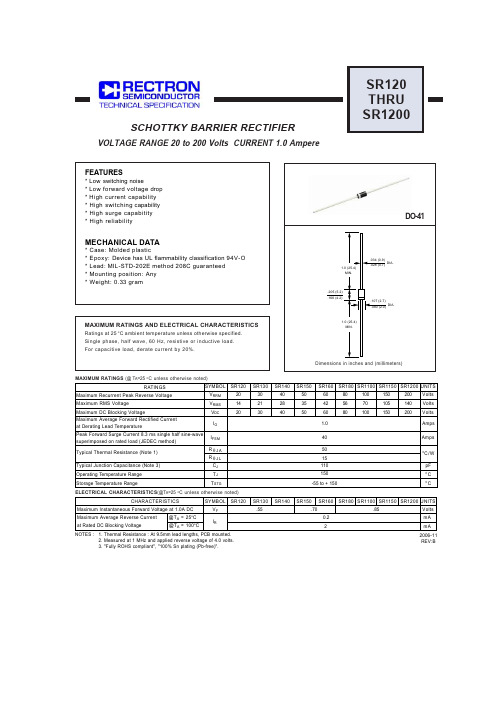
VOLTAGE RANGE 20 to 200 Volts CURRENT 1.0 AmpereDO-41MAXIMUM RATINGS (@ T A =25 O C unless otherwise noted)ELECTRICAL CHARACTERISTICS (@T A =25 OC unless otherwise noted)RATINGSMaximum Recurrent Peak Reverse Voltage Maximum RMS Voltage Maximum DC Blocking VoltageMaximum Average Forward Rectified Current at Derating Lead TemperaturePeak Forward Surge Current 8.3 ms single half sine-wave superimposed on rated load (JEDEC method)Typical Thermal Resistance (Note 1)Typical Junction Capacitance (Note 3)SYMBOL V RRM V DC I FSM C J T STG V RMS UNITS Volts Volts Volts Amps 1.0405015110AmpsC/W 0C Storage Temperature RangeR q J A R q J L I O pFOperating Temperature Range T J SR12020150-55 to + 150CSR130SR140SR150SR1603040506014212835422030405060SR180SR1100SR1150SR1200SR120SR130SR140SR150SR160SR180SR1100SR1150SR120080100150200801001502005670105140NOTES : 1. Thermal Resistance : At 9.5mm lead lengths, PCB mounted.2. Measured at 1 MHz and applied reverse voltage of 4.0 volts.3. "Fully ROHS compliant", "100% Sn plating (Pb-free)".2006-11REV:BCHARACTERISTICSMaximum Average Reverse Current at Rated DC Blocking VoltageV FSYMBOL I RmA Maximum Instantaneous Forward Voltage at 1.0A DC Volts 0.22@T A = 25o C @T A = 100oC.55mA UNITS.70.85PERCENT OF RATED PEAK REVERSE VOLTAGE, (%)INSTANTANEOUS FORWARD VOLTAGE, (V)I N S T A N T A N E O U S F O R W A R D C U R R E N T , (m A )LEAD TEMPERATURE, (OC)A V E R A G E F O R W A R D C U R R E N T , (A )C J , J U N C T I O N C A P A C I T A N C E , (p F )0.250.500.751.001.251501005000.11.01050RATING AND CHARACTERISTICS CURVES ( SR120 THRU SR1200 )FIG.3 TYPICAL INSTANTANEOUS FORWARD CHARACTERISTICSFIG.1 TYPICAL FORWARD CURRENT DERATING CURVEFIG.2 TYPICAL REVERSE CHARACTERISTICSREVERSE VOLTAGE, (V)I N S T A N T A N E O U S R E V E R S E C U R R E N T , (A )1080604020100200400FIG.4 TYPICAL JUNCTION CAPACITANCENUMBER OF CYCLES AT 60HzP E A K F O R W A R D S U R G E C U R R E N T , (A )1003020406050FIG.5 MAXIMUM NON-REPETITIVE FORWARD SURGE CURRENTRectron Inc reserves the right to make changes without notice to any productspecification herein, to make corrections, modifications, enhancements or other changes. Rectron Inc or anyone on its behalf assumes no responsibility or liabi- lity for any errors or inaccuracies. Data sheet specifications and its information contained are intended to provide a product description only. "Typical" paramet- ers which may be included on RECTRON data sheets and/ or specifications ca- n and do vary in different applications and actual performance may vary over ti- me. Rectron Inc does not assume any liability arising out of the application or use of any product or circuit.Rectron products are not designed, intended or authorized for use in medical, life-saving implant or other applications intended for life-sustaining or other rela- ted applications where a failure or malfunction of component or circuitry may di- rectly or indirectly cause injury or threaten a life without expressed written appr- oval of Rectron Inc. Customers using or selling Rectron components for use in such applications do so at their own risk and shall agree to fully indemnify Rect- ron Inc and its subsidiaries harmless against all claims, damages and expendit- ures.DISCLAIMER NOTICE。
AP90T03GR资料
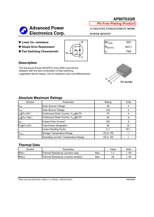
N-CHANNEL ENHANCEMENT MODE Electronics Corp.POWER MOSFET▼Lower On- resistance BV DSS 30V ▼ Simple Drive Requirement R DS(ON)4m Ω▼ Fast Switching CharacteristicI D75ADescriptionAbsolute Maximum RatingsSymbolUnits V DS V V GSV I D @Tc=25℃A I D @Tc=100℃A I DMA P D @Tc=25℃W W/℃T STG ℃T J℃SymbolValue Units Rthj-c Thermal Resistance Junction-case Max. 1.3℃/W Rthj-aThermal Resistance Junction-ambientMax.62℃/WData and specifications subject to change without notice200120041AP90T03GRPb Free Plating ProductParameterRating Drain-Source Voltage 30Gate-Source Voltage±20Continuous Drain Current, V GS @4.5V 75Continuous Drain Current, V GS @4.5V 63Pulsed Drain Current 1350Total Power Dissipation 96-55 to 150Operating Junction Temperature Range-55 to 150Linear Derating Factor 0.7Thermal DataParameterStorage Temperature RangeThe Advanced Power MOSFETs from APEC provide the designer with the best combination of fast switching,ruggedized device design, low on-resistance and cost-effectiveness.G DSTO-262(R)Electrical Characteristics@T j=25o C(unless otherwise specified) Symbol Parameter Test Conditions Min.Typ.Max.UnitsBV DSS Drain-Source Breakdown Voltage V GS=0V, I D=1mA30--V ΔB V DSS/ΔT j Breakdown Voltage Temperature Coefficient Reference to 25℃, I D=1mA-0.02-V/℃R DS(ON)Static Drain-Source On-Resistance2V GS=10V, I D=45A--4mΩV GS=4.5V, I D=30A--6mΩV GS(th)Gate Threshold Voltage V DS=V GS, I D=250uA0.8-3V g fs Forward Transconductance V DS=10V, I D=30A-55-S I DSS Drain-Source Leakage Current (Tj=25o C)V DS=30V, V GS=0V--1uA Drain-Source Leakage Current (T j=150o C)V DS=24V ,V GS=0V--25uAI GSS Gate-Source Leakage VGS= ±20V--±100nA Q g Total Gate Charge2I D=40A-6096nC Q gs Gate-Source Charge V DS=24V-8.5-nC Q gd Gate-Drain ("Miller") Charge V GS=4.5V-38-nC t d(on)Turn-on Delay Time2V DS=15V-14-ns t r Rise Time I D=30A-83-ns t d(off)Turn-off Delay Time R G=3.3Ω,V GS=10V-66-ns t f Fall Time R D=0.5Ω-120-ns C iss Input Capacitance V GS=0V-40906540pF C oss Output Capacitance V DS=25V-1010-pF C rss Reverse Transfer Capacitance f=1.0MHz-890-pF Source-Drain DiodeSymbol Parameter Test Conditions Min.Typ.Max.Units V SD Forward On Voltage2I S=45A, V GS=0V-- 1.3V trr Reverse Recovery Time I S=30A, V GS=0V,-51-ns Qrr Reverse Recovery Charge dI/dt=100A/µs-63-nCNotes:1.Pulse width limited by safe operating area.2.Pulse width <300us , duty cycle <2%.AP90T03GRAP90T03GRFig 2. Typical Output CharacteristicsFig 3. On-Resistance v.s. Gate VoltageFig 4. Normalized On-Resistance v.s. Junction TemperatureFig 5. Forward Characteristic ofFig 6. Gate Threshold Voltage v.s.Reverse DiodeJunction TemperatureFig 7. Gate Charge Characteristics Fig 8. Typical Capacitance CharacteristicsFig 9. Maximum Safe Operating Area Fig 10. Effective Transient Thermal ImpedanceFig 11. Switching Time Waveform Fig 12. Gate Charge WaveformAP90T03GR。
P1641100;中文规格书,Datasheet资料
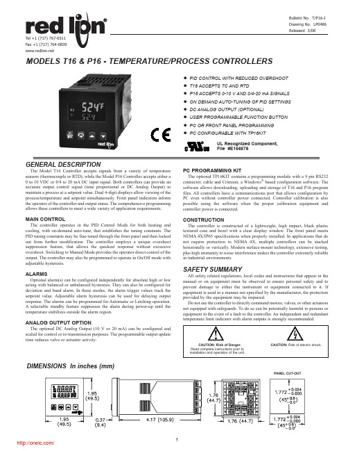
GENERAL DESCRIPTIONThe Model T16 Controller accepts signals from a variety of temperature sensors (thermocouple or RTD), while the Model P16 Controller accepts either a 0 to 10 VDC or 0/4 to 20 mA DC input signal. Both controllers can provide an accurate output control signal (time proportional or DC Analog Output) to maintain a process at a setpoint value. Dual 4-digit displays allow viewing of the process/temperature and setpoint simultaneously. Front panel indicators inform the operator of the controller and output status. The comprehensive programming allows these controllers to meet a wide variety of application requirements.MAIN CONTROLThe controller operates in the PID Control Mode for both heating and cooling, with on-demand auto-tune, that establishes the tuning constants. The PID tuning constants may be fine-tuned through the front panel and then locked out from further modification. The controller employs a unique overshoot suppression feature, that allows the quickest response without excessive overshoot. Switching to Manual Mode provides the operator direct control of the output. The controller may also be programmed to operate in On/Off mode with adjustable hysteresis.ALARMSOptional alarm(s) can be configured independently for absolute high or low acting with balanced or unbalanced hysteresis. They can also be configured for deviation and band alarm. In these modes, the alarm trigger values track the setpoint value. Adjustable alarm hysteresis can be used for delaying output response. The alarms can be programmed for Automatic or Latching operation.A selectable standby feature suppresses the alarm during power-up until the temperature stabilizes outside the alarm region.ANALOG OUTPUT OPTIONThe optional DC Analog Output (10 V or 20 mA) can be configured and scaled for control or re-transmission purposes. The programmable output update time reduces valve or actuator activity.PC PROGRAMMING KITThe optional TP16KIT contains a programming module with a 9 pin RS232connector, cable and Crimson, a Windows ®based configuration software. The software allows downloading, uploading and storage of T16 and P16 program files. All controllers have a communications port that allows configuration by PC even without controller power connected. Controller calibration is also possible using the software when the proper calibration equipment and controller power is connected.CONSTRUCTIONThe controller is constructed of a lightweight, high impact, black plastic textured case and bezel with a clear display window. The front panel meets NEMA 4X/IP65 specifications when properly installed. In applications that do not require protection to NEMA 4X, multiple controllers can be stacked horizontally or vertically. Modern surface-mount technology, extensive testing,plus high immunity to noise interference makes the controller extremely reliable in industrial environments.SAFETY SUMMARYAll safety related regulations, local codes and instructions that appear in the manual or on equipment must be observed to ensure personal safety and to prevent damage to either the instrument or equipment connected to it. If equipment is used in a manner not specified by the manufacturer, the protection provided by the equipment may be impaired.Do not use the controller to directly command motors, valves, or other actuators not equipped with safeguards. To do so can be potentially harmful to persons or equipment in the event of a fault to the controller. An independent and redundant temperature limit indicator with alarm outputs is strongly recommended.z PID CONTROL WITH REDUCED OVERSHOOT z T16 ACCEPTS TC AND RTDz P16 ACCEPTS 0-10 V AND 0/4-20 mA SIGNALS z ON DEMAND AUTO-TUNING OF PID SETTINGS z DC ANALOG OUTPUT (OPTIONAL)z USER PROGRAMMABLE FUNCTION BUTTON z PC OR FRONT PANEL PROGRAMMING z PC CONFIGURABLE WITH TP16KITDIMENSIONS In inches (mm)PANEL CUT-OUTUL Recognized Component,File #E156876INPUT SPECIFICATIONS1. SENSOR INPUT:Sample Period: 100 msec (10 Hz rate)Step Response Time: 300 msec typical, 400 msec max to within 99% of final value with step input.Failed Sensor Response:Main Control Output(s): Programmable preset outputDisplay: “OPEN”Alarms: Upscale driveAnalog Output: Upscale drive when assigned to retransmitted input. Normal Mode Rejection: >40 dB @ 50/60 HzCommon Mode Rejection: >120 dB, DC to 60 HzOvervoltage Protection: 120 V AC @ 15 sec max2. RTD INPUTS: (T16 only)Type: 2 or 3 wireExcitation: 150 µA typicalLead Resistance: 15 Ωmax per input leadResolution: 1° or 0.1° for all types 3. THERMOCOUPLE INPUTS: (T16 only)Types: T, E, J, K, R, S, B, N, C, and Linear mVInput Impedance: 20 MΩfor all typesLead Resistance Effect: 0.25 µV/ΩCold Junction Compensation: Less than ±1°C typical (1.5°C max) error over ambient temperature range.Resolution: 1° for types R, S, B and 1° or 0.1° for all other typesGENERAL SPECIFICATIONS1. DISPLAY: 2 Line by 4-digit, LCD negative image transmissive with backlighting.Top (Process) Display: 0.3" (7.6 mm) high digits with red backlighting. Bottom (Parameter) Display: 0.2" (5.1 mm) high digits with green backlighting.2. ANNUNCIATORS:Status Annunciators:O1 - Main control output is active.O2 - Cooling output is active (when Alarm 2 is used for cooling).A1 - Alarm 1 output is active.A2 - Alarm 2 output is active.°F, °C - Temperature units.%PW- Output power percentage is shown in Bottom display.MAN - Controller is in Manual Mode.R - Ramping Setpoint indicator.% - Percent indicator (P16 models only).Display Messages:OLOL- Measurement exceeds + sensor rangeULUL- Measurement exceeds - sensor rangeOPEN- Open sensor is detected (T16 only)SHrt- Shorted sensor is detected (RTD only)SENS- Measurement exceeds controller limits (P16 only)dddd- Display value exceeds + display range-ddd- Display value exceeds - display range3. POWER:Line Voltage Models:85 to 250 V AC, 50/60 Hz, 8 V ALow Voltage Models:DC Power: 18 to 36 VDC, 4 WAC Power: 24 V AC, ±10%, 50/60 Hz, 7 V A4. CONTROLS: Three rubber push buttons for modification and setup of controller parameters. One additional button (F1) for user programmable function. One external user input (models with alarms) for parameter lockout or other user programmable functions.5. MEMORY: Nonvolatile E2PROM retains all programmable parameters.6. ISOLATION LEVEL:AC power with respect to all other I/O: 250 V working (2300 V for 1 min.) Sensor input to analog output: 50 V working (500 V for 1 minute)Relay contacts to all other I/O: 300 V working (2300 V for 1 minute)DC power with respect to sensor input and analog output: 50 V working (500 V for 1 minute)7. CERTIFICATIONS AND COMPLIANCES:SAFETYUL Recognized Component, File #E156876, UL873, CSA22.2 No. 24Recognized to US and Canadian requirements under the ComponentRecognition Program of Underwriters Laboratories, Inc.Type 4X Enclosure rating (Face only), UL50IEC 61010-1, EN 61010-1: Safety requirements for electrical equipmentfor measurement, control, and laboratory use, Part IIP65 Enclosure rating (Face only), IEC529 ELECTROMAGNETIC COMPATIBILITYNotes:1. Self-recoverable loss of performance during EMI disturbance at 10 V/m:Measurement input signal may deviate during EMI disturbance.For operation without loss of performance:Install one ferrite core one turn, RLC #FCOR0000 or equivalent, to I/Ocables at unit.2. Self-recoverable loss of performance during EMI disturbance at 10 Vrms:Process and analog output signal may deviate during EMI disturbance. For operation without loss of performance:Install one ferrite core one turn, RLC #FCOR0000 or equivalent, to I/Ocables and power cable at unit.Refer to the EMC Installation Guidelines section of this bulletin for additional information.8. ENVIRONMENTAL CONDITIONS:Operating Temperature Range: 0 to 50°CStorage Temperature Range: -40 to 80°COperating and Storage Humidity: 85% max relative humidity (non-condensing) from 0°C to 50°CVibration According to IEC 68-2-6: Operational 5 to 150 Hz, in X, Y, Z direction for 1.5 hours, 2 g’s.Shock According to IEC 68-2-27: Operational 20 g’s (10 g relay), 11 msec in 3 directions.Altitude: Up to 2000 meters9. CONNECTION: Wire-clamping screw terminals10. CONSTRUCTION: Black plastic alloy case and collar style panel latch. Panel latch can be installed for vertical or horizontal instrument stacking. Black plastic textured bezel with transparent display window. Controller meets NEMA4X/IP65 requirements for indoor use when properly installed. Installation Category II, Pollution Degree 2.11. WEIGHT: 6.3 oz (179 g)Emissions to EN 50081-2Enclosure class AEN 55011RF interference150 KHz - 80 MHzLevel 3; 10 V/rms 2EN 61000-4-6RF conducted interferenceLevel 3; 2 kV powerLevel 4; 2 kV I/OEN 61000-4-4Fast transients (burst)80 MHz - 1 GHzLevel 3; 10 V/m 1EN 61000-4-3Electromagnetic RF fieldsLevel 2; 4 kV contactLevel 3; 8 kV airEN 61000-4-2Electrostatic dischargeImmunity to EN 50082-2Power mains class AOUTPUT SPECIFICATIONS1. CONTROL AND ALARM OUTPUTS:Relay Output:Type:Form AContact Rating:3 A@ 250 V AC or 30 VDC; 1/10 HP@ 120 V AC (inductive load)Life Expectancy:100,000 cycles at max. load rating(Decreasing load and/or increasing cycle time, increases life expectancy) Logic/SSR Output (main control output only):Rating: 45 mA max @ 4 V min., 7 V nominal2. MAIN CONTROL:Control: PID or On/OffOutput: Time proportioning or DC AnalogCycle Time: ProgrammableAuto-Tune: When selected, sets proportional band, integral time, derivative time, and output dampening time. Also sets input filter and (if applicable) cooling gain.Probe Break Action: Programmable3.ALARMS: (optional) 2 relay alarm outputs.Modes:NoneAbsolute High Acting (Balanced or Unbalanced Hysteresis)Absolute Low Acting (Balanced or Unbalanced Hysteresis)Deviation High ActingDeviation Low ActingInside Band ActingOutside Band ActingHeat (Alarm 1 on Analog Output models only)Cool (Alarm 2)Reset Action: Programmable; automatic or latchedStandby Mode: Programmable; enable or disableHysteresis: ProgrammableSensor Fail Response: UpscaleAnnunciator: “A1” and “A2” programmable for normal or reverse acting 4. COOLING: Software selectable (overrides Alarm 2).Control: PID or On/OffOutput: Time proportioningCycle Time: ProgrammableProportional Gain Adjust: ProgrammableHeat/Cool Deadband Overlap: Programmable5. ANALOG DC OUTPUT: (optional)Action: Control or retransmissionUpdate Rate: 0.1 to 250 secafter 20 minute warm-up.**Outputs are independently jumper selectable for either 10 V or 20 mA. The output range may be field calibrated to yield approximately 5% overrange and a small underrange (negative) signal.INPUT SPECIFICATIONS (Cont’d) 4.*after 20 minute warm-up.5. TEMPERATURE INDICATION ACCURACY: (T16 only)± (0.3% of span, +1°C) at 23 °C ambient after 20 minute warm up. Includes NIST conformity, cold junction effect, A/D conversion errors and linearization conformity.Span Drift (maximum): 130 PPM/°C6. USER INPUT: (Only controllers with alarms have a user input terminal.) Internally pulled up to +7 VDC (100 KΩ), V IN MAX= 35 V, V IL= 0.6 V max, V IH= 1.5 V min, I OFF= 40 µA maxResponse Time: 120 msec maxFunctions: ProgrammableEMC INSTALLATION GUIDELINESAlthough this controller is designed with a high degree of immunity to Electromagnetic Interference (EMI), proper installation and wiring methods must be followed to ensure electromagnetic compatibility (EMC) in each application. The type of the electrical noise, source or coupling method into the controller may be different for various installations. The controller becomes more immune to EMI with fewer I/O connections. Cable length, routing, and shield termination are very important and can mean the difference between a successful or troublesome installation. Listed are some EMC guidelines for successful installation in an industrial environment.1. The controller should be mounted in a metal enclosure that is properly connected to protective earth.2. Use shielded (screened) cables for all Signal and Control inputs. The shield (screen) pigtail connection should be made as short as possible. The connection point for the shield depends somewhat upon the application. Listed below are the recommended methods of connecting the shield, in order of their effectiveness.a. Connect the shield only at the panel where the controller is mounted toearth ground (protective earth).b. Connect the shield to earth ground at both ends of the cable, usually whenthe noise source frequency is more than 1 MHz.c. Connect the shield to common of the controller and leave the other end ofthe shield unconnected and insulated from earth ground.3. Never run Signal or Control cables in the same conduit or raceway with AC power lines, conductors feeding motors, solenoids, SCR controls, and heaters, etc. The cables should be run through metal conduit that is properly grounded. This is especially useful in applications where cable runs are long and portable two-way radios are used in close proximity or if the installation is near a commercial radio transmitter.4. Signal or Control cables within an enclosure should be routed as far away as possible from contactors, control relays, transformers, and other noisy components.5. In extremely high EMI environments, the use of external EMI suppression devices, such as ferrite suppression cores, is effective. Install them on Signal and Control cables as close to the controller as possible. Loop the cable through the core several times or use multiple cores on each cable for additional protection. Install line filters on the power input cable to the controller to suppress power line interference. Install them near the power entry point of the enclosure. The following EMI suppression devices (or equivalent) are recommended:Ferrite Suppression Cores for Signal and Control cables:Fair-Rite # 0443167251 (Red Lion Controls # FCOR0000)TDK # ZCAT3035-1330ASteward # 28B2029-0A0Line Filters for input power cables:Schaffner # FN610-1/07 (Red Lion Controls # LFIL0000)Schaffner # FN670-1.8/07Corcom # 1 VR3Note: Reference manufacturer’s instructions when installing a line filter. 6. Long cable runs are more susceptible to EMI pickup than short cable runs. Therefore, keep cable runs as short as possible.7. Switching of inductive loads produces high EMI. Use of snubbers across inductive loads suppresses EMI.Snubber: Red Lion Controls # SNUB0000.setting is formA.use to provide a watertight seal in steel panels with a minimum thickness of 0.09", or aluminum panels with a minimum thickness of 0.12". The controllers are designed to be mounted into an enclosed panel.The bezel assembly must be in place during installation of the controller.1. Prepare the panel cutout to the proper dimensions.2. Remove the panel latch from the controller. Discard the cardboard sleeve.3. Carefully remove the center section of the panel gasket and discard. Slide the panel gasket over the rear of the controller, seating it against the lip at the front of the case.4. Insert the controller into the panel cutout. While holding the controller in place, push the panel latch over the rear of the controller, engaging the tabs of the panel latch in the farthest forward slot possible.effectiveness of the seal.may affect proper operation.Multiple Controller StackingThe controller is designed to allow for close spacing of multiple controllers in applications that do not require protection to NEMA 4X. Controllers can be stacked either horizontally or vertically. For vertical stacking, install the panel latch with the screws to the sides of the controller. For horizontal stacking, the panel latch screws should be at the top and bottom of the controller. The minimum spacing from centerline to centerline of controllers is 1.96" (49.8mm). This spacing is the same for vertical or horizontal stacking.Note: When stacking controllers, provide adequate panelventilation to ensure that the maximum operating temperature range is not exceeded.WIRING CONNECTIONSAll wiring connections are made to the rear screw terminals. When wiring the controller, use the numbers on the label and those embossed on the back of the case, to identify the position number with the proper function.All conductors should meet voltage and current ratings for each terminal. Also, cabling should conform to appropriate standards of good installation, local codes and regulations. It is recommended that power (AC or DC) supplied to the controller be protected by a fuse or circuit breaker. Strip the wire, leaving approximately 1/4" (6 mm) bare wire exposed (stranded wires should be tinned with solder). Insert the wire under the clamping washer and tighten the screw until the wire is clamped tightly.CONTROLLER POWER CONNECTIONS For best results, the power should be relatively “clean” and within the specified limits. Drawing power from heavily loaded circuits orfrom circuits that also power loads that cycle on and off should be avoided. It is recommended that power supplied to the controller beprotected by a fuse or circuit breaker.INPUT CONNECTIONSFor two wire RTDs, install a copper sense lead of the same gauge and length as the RTD leads. Attach one end of the wire at the probe and the other end to input common terminal. Complete lead wire compensation is obtained. This is the preferred method. If a sense wire is not used, then use a jumper. A temperature offset error will exist. The error may be compensated byprogramming a temperature offset.VDC VACRTD and Resistance Voltage and CurrentFRONT PANEL KEYSThe F1 key is pressed to exit (or escape) directly to the start of the Display Loop. While in the Display Loop, the F1 key can be pressed to activate its programmed function.The Loop key is pressed to advance to the next parameter, to activatea changed selection/value, and when held for three seconds, enter theHidden Loop.The Arrow keys are used to scroll through parameter selections/values and in the Configuration Loop they are used to scroll to the appropriate Parameter Module.Note: Setpoint and Output Power are the only parameters visible in the Display Loop with Factory Settings. The remaining parameters can be selected for the Display Loop within Module 3.Parameter availability is model and programming dependent.DISPLAY LOOPAt power up, all display segments light, and then the programmed input type and the controller’s software version will flash. Then the Temperature/Process Value is shown in the top display, and the Setpoint Value is shown in the bottom display. This is the Display Loop. If the Setpoint is hidden or locked, the Display Loop will default to Output Power. If Output Power is also hidden or locked out, the bottom display is blank. During programming, the F1 key can be pressed to return the controller to this point. (Only in the Display Loop will the F1 key perform the user function programmed in Input Module .)When the is pressed the controller advances to the next parameter in the Display Loop. Except for Setpoint and % Output Power, the bottom display alternates between the parameter name and its selection/value. The arrow keys are pressed to change the selection/value for the shown parameter. The new selection/value is activated when the is pressed. Display Loop parameters may be locked out or hidden in Lockout Module . Some parameters aremodel and programming dependent.SETPOINT VALUE (SP1) *SETPOINT VALUE (SP2) *-999to 99990.0OP% OUTPUT POWER *-100to 100.0-999to 9999Typically, the controller is operating with the Setpoint value in the bottom display. There is no annunciator nor parameter indication for Setpoint in theDisplay Loop. The parameter name alternates with the setpoint value in the Hidden Loop. The Setpoint value can be changed, activated and stored by pressing the arrow keys. This is the only parameter that can be configured as read only in the Display Loop, but read/write in the Hidden Loop. It is possible to store a second Setpoint value that can be selected in the Hidden Loop, by the F1 key or the user input. Both Setpoint values are limited by the Setpoint Low and High Limits in Input Module .The % Output Power is shown with the %PW annunciator. The parameter name alternates with the % Output Power value in the Hidden Loop. While the controller is in Automatic Mode, this value is read only. When the controller is placed in Manual Mode, the value can be changed, activated and stored by pressing the arrow keys. For more details on % Output Power, see Control Mode Explanations.INTEGRAL TIME0to 9999secondsIntegral action shifts the center point position of the proportional band toeliminate error in the steady state. The higher the integral time, the slower the response. The optimal integral time is best determined during PID Tuning. Iftime is set to zero, the previous Integral output power value is maintained.Offset Power can be used to provide Manual Reset.Derivative time helps to stabilize the response, but too high of a derivative time, coupled with noisy signal processes, may cause the output to fluctuate too greatly, yielding poor control. Setting the time to zero disables derivative action.ALARM 1 VALUE-999to 9999On models with alarms, the value for Alarm 1 can be entered here. The value is either absolute (absolute alarm types) or relative to the Setpoint value (deviation and band alarm types.) When Alarm 1 is programmed for HEAt or NonE , this parameter is not available. For more details on alarms, see Alarm Module "-.When the Integral Time is set to zero and the controller is in the Automatic Mode, this parameter will appear after % Output Power. It is also shown with the %PW annunciator illuminated. The power offset is used to shift the proportional band to compensate for errors in the steady state. If Integral Action is later invoked, the controller will re-calculate the internal integral value to provide “bumpless” transfer and Output Power Offset will not be necessary.The proportional band should be set to obtain the best response to a process disturbance while minimizing overshoot. A proportional band of 0.0% forces the controller into On/Off Control with its characteristic cycling at Setpoint. For more information, see Control Mode and PID Tuning Explanations.* Alternating indication only used in the Hidden Loop.ALARM 2 VALUE-999to 9999On models with alarms, the value for Alarm 2 can be entered here. The value is either absolute (absolute alarm types) or relative to the Setpoint value (deviation and band alarm types.) When Alarm 2 is programmed for CooL or NonE , this parameter is not available. For more details on alarms, see the Alarm Module 4-AL .The values shown for the displays are the factory settings.HIDDEN LOOPTo enter Hidden Loop, press for 3 seconds.HIDDEN LOOPWhen is pressed and held for three seconds, the controller advances to the Hidden Loop. The Temperature/Process Value is shown in the top display. The bottom display alternates between the parameter and its selection/value. or is pressed to change the selection/value for the shown parameter. The new selection/value is activated after is pressed. When is pressed, the controller returns to the Display Loop and stores changed selection/values to permanent memory. Hidden Loop parameters may be locked out in Lockout Module 3-LC . Some parameters are model and programming dependent.ª«CodEACCESS CODE1to 125If the Access Code is set from 1 to 125, in Lockout Module , Access Code will appear here. By entering the proper Code, access to the Hidden Loop is permitted. With the factory setting of 0, Access Code will not appear in the Hidden Loop. A universal code of 111 can be entered to gain access,independent of the programmed code number.The SPSL function allows the operator to switch from or to, setpoint 1 and setpoint 2. In the Display Loop, there is no annunciator indicating the selected Setpoint, however, the selected Setpoint value is displayed and activated.In Automatic Mode, the percentage of Output Power is automatically determined by the controller. In Manual/User USEr Mode, the percentage of Output Power is adjusted manually while in the Display Loop. The Control Mode can also be transferred through the F1 Key or User Input. For more information, see Control Mode Explanations.The setpoint ramp rate can reduce sudden shock to the process and reduce overshoot on startup or after setpoint changes, by ramping the setpoint at a controlled rate. R annunciator flashes while ramping. With the T16, the ramp rate is always in tenths of degrees per minute, regardless of the resolution chosen for the process display. With the P16, the ramp rate is in least-significant (display units) digits per minute. A value of 0.0 or 0 disables setpoint ramping. Once the ramping setpoint reaches the target setpoint, the setpoint ramp rate disengages until the setpoint is changed again. If the ramp value is changed during ramping,the new ramp rate takes effect. If the setpoint is ramping prior to starting Auto-Tune, the ramping is suspended during Auto-Tune and then resumed afterward.Deviation and band alarms are relative to the target setpoint, not the ramping setpoint. A slow process may not track the programmed setpoint rate. At power up, the ramping setpoint is initialized at the ambient temperature/process value.To access the Configuration Loop, press the up key when CNFP /NO is displayed in the Hidden Loop. The arrow keys are used to select the parameter module (1-9). To enter a specific module press while the module number is displayed.In the Configuration Loop, CNFP will alternate with the parameter number in the bottom display. The Temperature/Process Value is shown in the top display.After entering a parameter module, press to advance through the parameter names in the module. To change a parameter’s selection/value, press the arrow keys while the parameter is displayed. In the modules, the top display shows the parameter name, and the bottom display shows the selection/e to enter any selection/values that have been changed. The change is not committed to permanent memory until the controller is returned to the Display Loop. If a power loss occurs before returning to the Display Loop, the new values must be entered again.At the end of each module, the controller returns to CNFP /NO . At this location,pressing again returns the display to the the Display Loop. Pressing the Up key allows re-entrance to the Configuration Loop. Whenever is pressed, End momentarily appears as the parameters are stored to permanent memory and thecontroller returns to the Display Loop.ª«1-2ALrS ALARMS RESET1-2With alarm models, the alarms can be manually reset. The up key resets Alarm 1 and the down key resets Alarm 2.ACCESS CODE-1to -125If the Access Code is set from -1 to -125, in Lockout Module 3-LC , Access Code will appear here. By entering the proper Code, access to the Configuration Loop is permitted (with a negative Code value, the Hidden Loop can be accessed without the use of a code). With the factory setting of 0 or with an active User Input configured for Program Lock (PLOC ), Access Code will not appear here. An active user input configured for Program Lock (PLOC ) always locks out the Configuration Loop, regardless of Access Code.The Auto-Tune procedure of the controller sets the Proportional Band,Integral Time, Derivative Time, Digital Filter, Control Output Dampening Time, and Relative Gain (Heat/Cool) values appropriate to the characteristics of the process. This parameter allows front panel starting YES or stopping NO of Auto-Tune. For more information, see PID Tuning Explanations.。
TEA1716中文资料免费版
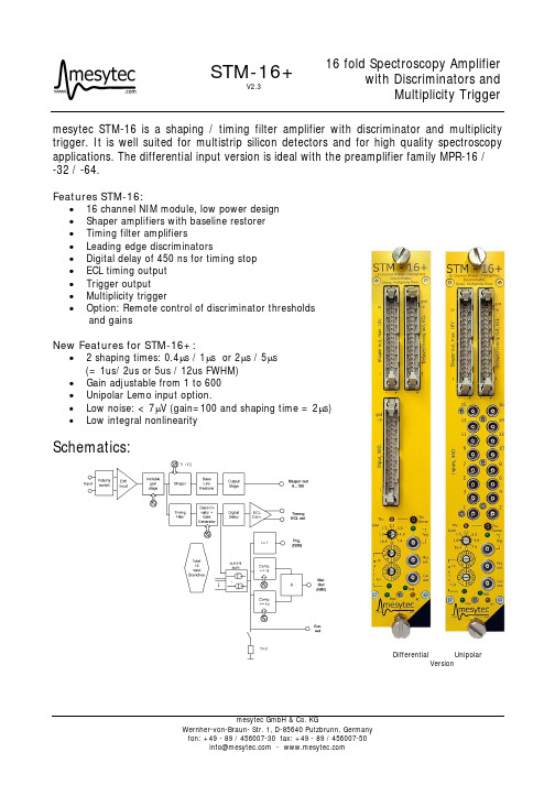
TEA1716T中文资料免费版1. General descriptionTEA1716T集成了功率因数校正器(PFC)控制器和半桥谐振变换器的控制器(HBC)multi-chip IC。
它提供了离散MOSFET的驱动功能在一个上升变换器和两个离散功率场效应管谐振半桥配置。
高效PFC操作是通过实现准谐振软开关技术(QR)操作功能在高功率水平与QR操作谷跳跃在低功率水平。
过电流保护(OCP)、过电压保护装置(OVP)和退磁传感在所有条件下确保安全运行。
HBC模块是一个高压零开关LLC谐振变换器的控制器。
它包含一个高压电平转变电路和保护电路包括OCP,开环保护,电容模式保护和通用门锁保护输入。
高压芯片制作用的是专用高压Bipolar-CMOS-DMOS功率逻辑处理能够有效的从电源电压直接启动。
低压绝缘硅片(SOI)芯片用于准确、高速的保护功能和控制。
TEA1716T控制PFC电路和谐振转换器是非常灵活的。
它可以用于广泛的应用在一个宽的电源电压范围。
PFC和HBC控制器结合在一个单一的电源控制IC 使TEA1716T理想在液晶和等离子电视。
使用TEA1716T提供高效、可靠的电力供应从90 W到500 W可以轻松地使用TEA1716T设计,用最少的外部组件。
TEA1716T的集成突发模态和电源管理功能使共振的应用程序满足能源使用产品指令(EuP)很多6(< 0.5 W在待机模式)。
2.1 General features集成PFC和HBC控制器通用电源运行从70V-276V (AC)高水平的集成导致较低的外部组件数量和成本效益的设计集成突发模式感应符合能源使用产品指令(EuP)6使能输入只允许使能PFC或者PFC和HBC控制器芯片上的高压启动源独立运行或从DC源供应2.2 PFC controller features及时控制边界模式操作谷底和零电压开关以致最小损耗频率限制来减少开关损耗精确的增压调节用软启动和软停止的突发模式开关2.3 HBC controller features集成高压电平位移器可调节最大和最小频率半桥开关频率最大可达500KHz合适的非重叠时间突发模式开关2.4 Protection features安全系统故障条件下重启模式通用门锁保护输入对输出过电压保护或外部温度保护保护定时器超时并重启过温保护对两个控制器软启动欠电压保护给电源(断电),增压,IC供应和输出电压对两个控制器进行过流保护和调节对增高电压精确的过压保护对HBC控制器容性模式保护3. ApplicationsLCD电视等离子电视笔记本适配器台式机6.2 Pin descriptionCOMPPFC 1 PFC控制器频率补偿,外部链接到过滤器SNSMAINS 2 电源电压输入感应;外部连接分压电阻电源电压SNSAUXPFC 3 PFC消磁时间感应输入;外部连接到PFC的辅助绕组SNSCURPFC 4 PFC控制器为瞬时电流和软启动检测输入;外部连接到电流检测电阻和软启动过滤器SNSOUT 5 检测输入监测HBC输出电压;外部连接到辅助绕组SUPIC 6 SUPIC低压输入和输出的内部高压启动源;外部连接到辅助绕组HBC 或外部直流供电GATEPFC 7 PFC MOSFET 门极驱动输出PGND 8 电源地,HBC和PFC参考地SUPREG 9 管理SUPREG IC供应;内部调节器输出,输入驱动;外部连接到SUPREG缓冲电容器GATELS 10 HBC 低边MOSFET 门驱动输出n.c. 11 不连接SUPHV 12 内部高压启动源供应源高压输入;外部连接来提高电压GATEHS 13 HBC 高边MOSFET门驱动输出SUPHS 14 高端的驱动提供输入;外部连接到自举电容(CSUPHS)HB 15 参考高端驱动和半桥斜坡输入检测;外部连接到半桥节点HB的HBC mosfet之间(参见图17)n.c. 16 不连接SNSCURHBC 17 瞬时HBC检测输入;外部连接到谐振电流检测电阻SGND 18 信号地和IC参考地CFMIN 19 HBC最低频率设置;外部连接的电容器SNSBURST 20 突然停止激活检测输入;外部连接分压电阻SNSFB电压SNSFB 21 输出电压调节反馈检测输入;外部连接到光耦合器和上拉电阻SSHBC/EN 22 HBC软启动t时间和IC使能输入;使能PFC或PFC只或PFC和HBC控制器;外部连接到s软启动电容器,使下拉的信号RCPROT 23 保护定时器设置超时并重启;外部连接的电阻器和电容器SNSBOOST 24 检测输入增加电压调整;外部连接分压电阻提高电压7. Functional descriptionTEA1716T可以组合的功能如下:电源模块:IC供应管理。
VIPER100中文资料

Supply Voltage
Voltage Range Input
Voltage Range Input
Maximum Continuous Current Electrostatic discharge (R = 1.5 KΩ C = 100pF) Avalanche Drain-Source Current, Repetitive or Not-Repetitive (TC = 100 o C, Pulse Width Limited by TJ max, δ <1%) for VIPer100/SP for VIPer100A/ASP Power Dissipation at T c = 25oC
PENTAWATT HV (022Y)
VIPer100 (022Y) VIPer100A (022Y)
Pow erS O-10
VIPer100SP VIPer100ASP
PINS FUNCTIONAL DESCRIPTION
DRAIN PIN: Integrated power MOSFET drain pin. It provides internal bias current during start-up via an integrated high voltage current source which is switched off during normal operation. The device is able to handle an unclamped current during its normal operation, assuring self protection against voltage surges, PCB stray inductance, and allowing a snubberless operation for low output power.
SWP TSR-100说明书(流量)
配件
当您首次打开包装时请先确认以下事项,如果您收到的产品有误 或有缺失或仪表损坏,请在第一时间通知我公司或当地经销商。
配件清单
配件名称
LCD-TSR 无纸记录仪 LCD-TSR 无纸记录仪用户手册 固定卡条(出厂时以安装在仪表外壳上) 产品合格证书 产品保修证书
数量
1台 1本 2条 1份 1份
2 总机:021-5108 6685 传真:021-5186 2905
个继电器输出点,带 RS-232 通讯接口,配置 128Mbit 内存。
3 总机:021-5108 6685 传真:021-5186 2905
目录
第一章 概 述...............................................................................................................................6 第二章 主要技术指标 .......................................................................................................................9 第三章 安装与接线 ......................................................................................................................... 11
3.2.1 安装环境................................................................................................................11 3.2.2 安装尺寸................................................................................................................11 3.2.3 安装方法............................................................................................................... 12 3.3 仪表接线................................................................................................................................12 3.3.1 端子说明................................................................................................................ 13 3.3.2 接线说明................................................................................................................ 14 第四章 操作说明.............................................................................................................................19 4.1 上电........................................................................................................................................19 4.2 按键操作................................................................................................................................19 4.3 特殊功能组合键....................................................................................................................20 第五章 显示画面.............................................................................................................................21 5.1 实时多通道显示.....................................................................................................................21 5.2 当前报警显示.........................................................................................................................22 5.3 双通道数字显示.....................................................................................................................23 5.4 全通道实时数据显示 ............................................................................................................23 5.5 报警记录一览显示................................................................................................................24 5.6 棒形图显示............................................................................................................................24 5.7 历史记录追忆........................................................................................................................25 5.8 仪表配置及接线图画面 ........................................................................................................27 5.9 流量显示.................................................................................................................................28 5.10 掉电显示...............................................................................................................................28 5.11 日、月、班报表显示 ...........................................................................................................29 第六章 组态设置.............................................................................................................................30 6.1 基本操作方法........................................................................................................................30 6.2 组态菜单画面与仪表参数 .....................................................................................................32 6.2.1 系统组态............................................................................................................... 32
高性能开关电源同步整流芯片 LPSR100说明书

概述LPSR100为高性能的开关电源100V 同步整流系列产品,兼容多种开关电源控制系统。
LPSR100支持DCM 和CCM 多种工作模式。
LPSR100采用专利的整流管开通判定技术,可以有效的避免因激磁振荡引起的驱动芯片误开通。
LPSR100具有极快的关断速度,可以大幅度降低在CCM 工作条件下因关断延迟造成的效率损失。
LPSR100集成VCC 供电技术,在不需要辅助绕组供电的情况下,保证芯片VCC 不会欠压。
LPSR100采用TO220-3L/TO252-2L/SOP8L/PDFN5*6封装。
特点⏹开关电源同步整流应用⏹兼容DCM 和CCM 多种工作模式⏹内置100V 耐压功率管⏹专利的整流管开通技术⏹集成VCC 供电⏹芯片供电欠压保护⏹芯片过压钳位⏹外围元器件少应用⏹充电器和适配器的同步整流⏹正激控制器和反激控制器⏹其他开关电源控制系统典型应用图1LPSR100反激典型应用定购信息图2管脚封装图管脚描述A JA注3:人体模型,100pF电容通过1.5KΩ电阻放电。
电气参数(注4,5)(无特别说明情况下,V CC=6V,T A=25℃)电气特性图内部结构框图图3LPSR100内部框图应用信息LPSR100为高性能的开关电源100V 同步整流系列产品,兼容多种开关电源控制系统,支持DCM ,CCM 多种工作模式。
LPSR100采用专利的整流管开关技术,可以有效的避免因激磁振荡引起的驱动芯片误动作。
LPSR100集成VCC 供电技术,在不需要辅助绕组供电的情况下,保证芯片VCC 不会欠压。
启动当系统上电后,通过内置MOS 的体二极管对输出电容充电,输出电压上升。
LPSR100通过D 脚连接输出电压,当输出电压上升时,经过芯片内部供电电路,给VCC 电容充电,当VCC 的电压充到开启阈值电压时,芯片内部控制电路开始工作,MOS 正常的导通和关断。
MOS 正常的导通时,电流不再从体二极管流过,而从MOS 的沟道流过。
ER1603FCT中文资料(Won-Top Electronics)中文数据手册「EasyDatasheet - 矽搜」

标识信息
WTE
ER160xFCT WTE =制造商标志 ER160xFCT =设备号 x = 0,1,1A,2,3,4或6个 极性 =对人体标示
封装信息
BULK
管尺寸 长×宽×高(mm) 数量 内箱尺寸 长×宽×高(mm) 数量 外箱尺寸 长×宽×高(mm) 数量 约.总重量
(PCS) 50
(PCS) 2,000
6-32六角头螺丝
平焊盘圈
锥形焊盘圈应该用于正确力施加到所述设 备.螺钉不应收紧与任何类型空气被迫扭 矩或器材可能导致裂纹器件封装.
整流器 散热器 锥形焊盘圈
导热硅脂或接口散热焊盘一层将是散热相当 有帮助.
6-32六角螺母
ER1600FCT – ER1606FCT
3 of 4
芯片中文手册,看全文,戳
芯片中文手册,看全文,戳
ER1600FCT – ER1606FCT
16A玻璃钝化双超快速整流器 特征
玻璃钝化模具结构 超快速切换 低正向压降 低反向漏电流 高浪涌电流能力 塑料材料具有UL可燃性 分类94V-O
Pb
B C G
PIN1 2 3
A
D
机械数据
案例:ITO-220,全模制塑料 终端:每焊镀信息 MIL-STD-202,方法208 极性:见图 重量:2.24克(约) 安装位置:任意 安装扭矩:11.5厘米千克(10磅)最大. 无铅:对于符合 RoHS /无铅版本 , 新增 "-LF"后缀型号 ,见第 4页
循环次数在60Hz 图. 3最大不重复浪涌电流
10 10 100 0.1 1.0 VR,反向电压(V) 图. 4典型结电容
t +0.5A
10
100
FR16中文资料
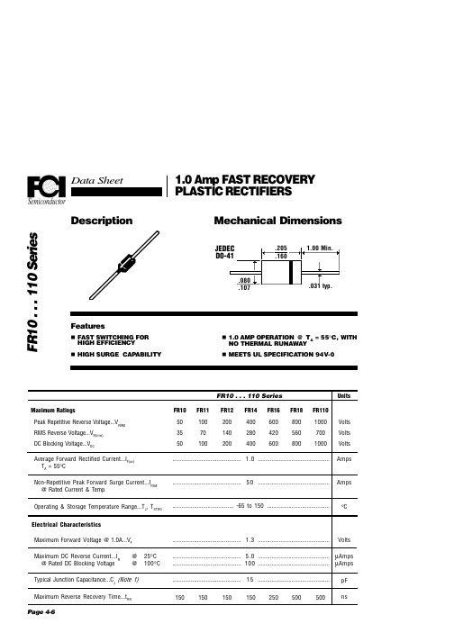
°C
Volts
............................................. 5.0 ............................................... µAmps ............................................. 100 ............................................... µAmps ............................................. 1 5 ............................................... 150 150 150 150 250 500 500 pF ns
Units
Volts Volts Volts Amps
............................................. 1.0 ...............................................
............................................. 5 0 ...............................................
1
1
10
100
1000
Number of Cycles @ 60 Hz
Typical Instantaneous Forward Characteristics 10 Forward Current (A) 100 50
电子温度开关ETS 1700及其配套温度探头TFP 100的产品说明书

E N 18.303.5/02.184Description:The electronic temperature switch ETS 1700 is used mainly together with the temperature probe TFP 100, which was specially developed for tank mounting.The 4-digit display can indicate the actual temperature, one of the switch points or the maximum temperature value.The maximum temperature indicates the highest temperature which has occurred since the unit was switched on or was last reset.The four switching outputs can be used to control heating and cooling processes in hydraulic systems, for example. Four switch and switch-back points which are independent of each other can be adjusted very simply via the key pad.For integration into monitoring systems (e.g. with PLC), an analogue output (4 .. 20 mA or 0 .. 10 V) is also available.Technical data:Input dataMeasuring elementPT 100 (TFP 100)Connection, separate temperature probe Male connector 5 pole Binder series 423/723Measuring range 1)0 .. +100 °C (+32 .. +212 °F)Output dataSwitching outputs4 relays with change-over contacts in 2 groups (common supply of each group connected)Switching current: 0.01 .. 2 A per switching output Switching voltage: 0.1 .. 250 V AC, 12 .. 32 V DC Switching capacity: 500 VA, 64 W (for inductive load, use varistors)Switching cycles (ohmic resistance): ≥ 20 million at minimum load ≥ 400000 at maximum load (typ.)Analogue output, permitted load resistanceSelectable:4 .. 20 mA load resist. max. 400 Ω 0 .. 10 V load resist. min. 2 kΩcorresponds in each case to 0 .. +100 °C Accuracy (at room temperature)≤ ± 1.0 °C (≤ ± 2.0 °F)(+error separate temperature probe)Temperature drift (environment)≤ ± 0.03 % FS / °C Repeatability≤ ± 0.25 % FSEnvironmental conditions Operating temperature range -25 .. +60 °C Storage temperature range-40 .. +80 °CmarkEN 61000-6-1 / 2 / 3 / 4Vibration resistance acc. to DIN EN 60068-2-6 (0 .. 500 Hz)≤ 5 g Shock resistance acc. to DIN EN 60068-2-27 (1 ms)≤ 10 g Protection class acc. to DIN EN 60529IP 65Other dataElectrical connection Plug-in terminal block, 14 pole Supply voltage22 .. 32 V DC Residual ripple of supply voltage ≤ 10 %Current consumption ~ 200 mADisplay4-digit, LED, 7-segment, red, height of digits 13 mmWeight ~ 800 gNote:Reverse polarity protection of the supply voltage, overvoltage, override and short circuitprotection are provided.FS (F ull S cale) = relative to complete measuring range 1)Depending on the fluid temperature range of the connected temperature sensor, the measuring range of the ETS 1700 may be reduced.Temperature SwitchETS 17004 switching outputs Analogue output258E N 18.303.5/02.184Setting options:The microprocessor integrated into the ETS 1700 enables many useful extrafunctions in addition to the switching functions, when compared with a normal mechanical temperature switch. It is possible, for example, to activate switching delay times or to change the relay switching direction. All settings are made via the key pad.Setting ranges of the switch points andswitch-back hystereses:●Switch point, relay 1 .. 4:1.5 .. 100 % of the measuring span ●Switch-back point, relay 1 .. 4: 1 .. 99 % of the measuring span or alternatively●Switch-back hysteresis 1 .. 4: 1 .. 99 % of the measuring spanAdditional functions:●Switching direction of the relays 1 .. 4 (N/C or N/O function)●Switch-on delay, relays 1 .. 4 in the range 0.0 .. 900.0 seconds●Switch-off delay, relays 1 .. 4 in the range 0.0 .. 900.0 seconds●Switch-back mode (alternatively switch-back point or switch-back hysteresis)●Display of the actual temperature, a switch point or the peak value●Measuring range individually selectable in °C or °F●Display of the measurement unit (°C, °F) ●Analogue output (4 .. 20 mA or 0 .. 10 V) ●Programming lockTerminal assignment:Device connection Pin 1+U B 20 V3Analogue output Signal +4Analogue output Signal - (0 V)5Relay 1 N/C 6Relay 1 N/O7Centre relay 1 and 28Relay 2 N/C 9Relay 2 N/O 10Relay 3 N/C 11Relay 3 N/O12Centre relay 3 and 413Relay 4 N/C 14Relay 4 N/OProbe connection Pin 1+U B2Signal +3n.c.4Signal -50 VDimensions:Screw type conduit fitting PG11Female connectorBinder series 423/723 -5pCountersunk to DIN74-KM5Note:The information in this brochure relates to the operating conditions and applications described.For applications or operating conditions not described, please contact the relevant technical department.Subject to technical modifications.HYDAC ELECTRONIC GMBHHauptstraße 27, 66128 Saarbrücken GermanyTelephone +49 (0)6897 509-01 Fax +49 (0)6897 509-1726 E-mail:********************Internet: 。
Pt100热电阻计算公式及分度表
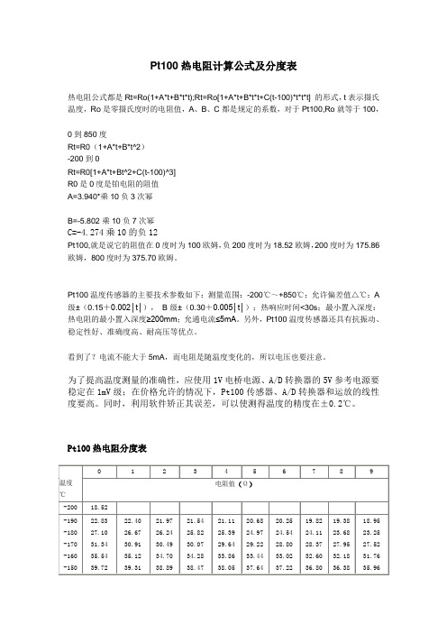
Pt100热电阻计算公式及分度表
热电阻公式都是Rt=Ro(1+A*t+B*t*t);Rt=Ro[1+A*t+B*t*t+C(t-100)*t*t*t] 的形式,t表示摄氏温度,Ro是零摄氏度时的电阻值,A、B、C都是规定的系数,对于Pt100,Ro就等于100,
0到850度
Rt=R0(1+A*t+B*t^2)
-200到0
Rt=R0[1+A*t+Bt^2+C(t-100)^3]
R0是0度是铂电阻的阻值
A=3.940*乘10负3次幂
B=-5.802乘10负7次幂
C=-4.274乘10的负12
Pt100,就是说它的阻值在0度时为100欧姆,负200度时为18.52欧姆,200度时为175.86欧姆,800度时为375.70欧姆。
Pt100温度传感器的主要技术参数如下:测量范围:-200℃~+850℃;允许偏差值△℃:A 级±(0.15+0.002│t│),B级±(0.30+0.005│t│);热响应时间<30s;最小置入深度:热电阻的最小置入深度≥200mm;允通电流≤5mA。
另外,Pt100温度传感器还具有抗振动、稳定性好、准确度高、耐高压等优点。
看到了?电流不能大于5mA,而电阻是随温度变化的,所以电压也要注意。
为了提高温度测量的准确性,应使用1V电桥电源、A/D转换器的5V参考电源要稳定在1mV级;在价格允许的情况下,Pt100传感器、A/D转换器和运放的线性度要高。
同时,利用软件矫正其误差,可以使测得温度的精度在±0.2℃。
Pt100热电阻分度表。
EN25F16-100HI资料
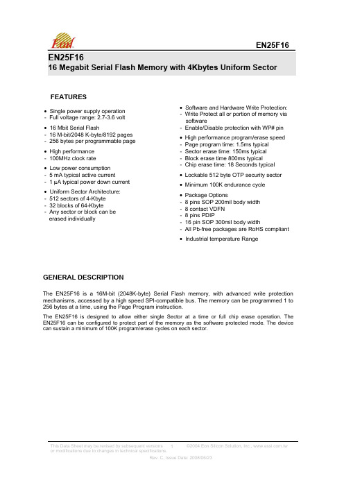
EN25F16
This Data Sheet may be revised by subsequent versions
3
or modifications due to changes in technical specifications.
Hale Waihona Puke ©2004 Eon Silicon Solution, Inc.,
Hold (HOLD#) The HOLD pin allows the device to be paused while it is actively selected. When HOLD is brought low, while CS# is low, the DO pin will be at high impedance and signals on the DI and CLK pins will be ignored (don’t care). The hold function can be useful when multiple devices are sharing the same SPI signals.
Rev. C, Issue Date: 2008/06/23
元器件交易网
MEMORY ORGANIZATION
EN25F16
The memory is organized as: z 2,097,152 bytes z Uniform Sector Architecture
This Data Sheet may be revised by subsequent versions
4
or modifications due to changes in technical specifications.
SMT电子元器件的认识和换算培训资料
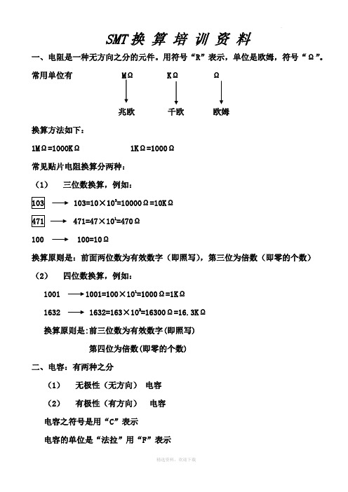
SMT换算培训资料一、电阻是一种无方向之分的元件。
用符号“R”表示,单位是欧姆,符号“Ω”。
常用单位有 MΩ KΩΩ兆欧千欧欧姆换算方法如下:1MΩ=1000KΩ 1KΩ=1000Ω常见贴片电阻换算分两种:(1)三位数换算,例如:103=10×103=10000Ω=10KΩ471 471=47×101=470Ω100100=10Ω换算原则是:前面两位数为有效数字(即照写),第三位为倍数(即零的个数)(2)四位数换算,例如:1001 1001=100×101=1000Ω=1KΩ16321632=163×102=16300Ω=16.3KΩ换算原则是:前三位数为有效数字(即照写)第四位为倍数(即零的个数)二、电容:有两种之分(1)无极性(无方向)电容(2)有极性(有方向)电容电容之符号是用“C”表示电容的单位是“法拉”用“F”表示常见单位有: F UF NF PF法拉微法拉法披法换算方法是:1F=106UF 1UF=106PF=1000000PF1NF=10×102=1000PF电容换算方法如下:104=10×104=100000PF= 0.1UF103=10×103=10000PF= 0.01UF10NF=10×103=10000PF= 0.01UF电容的误差表示,如:J ±5% D ±0.5% 330J:33PF±5%K ±10% F ±1% 102K:1000PF±10%M ±20% Z -20%+80% 104Z=0.1UF-20%+80% 三、电感电感之符号是用“L”表示电感的单位是亨利(简称亨),用字母"H"表示常用的单位: H mHμH nH亨毫亨微亨纳亨换算方法是:1H=1000mH;1mH=1000μH;1μH=1000nHWelcome !!! 欢迎您的下载,资料仅供参考!。
HT4906移动电源芯片

概述HT4906是一款集成了充电管理模块、电量检测及LED指示模块、升压放电管理模块,完全取代目前市场上的充电管理IC+MCU+升压IC方案。
应用◆移动电源◆IPAD,MID备用电源◆MP3,MP4,手机等数码产品的后备电源特点◆内置电量检测,4灯指示模式,充电时跑马灯指示显示模式◆放电时,电量指示灯一直显示当前锂电池电量,电量指示灯单向递减,直到关机熄灭◆线性充电模式,内置MOSFET,可外扩三极管充电。
支持对0V电池充电,涓流/恒流/恒压三段式充电。
◆内置充电电流具有过温补偿◆充电外扩具有软开关功能◆升压电路使用外部MOSFET◆手机插入自动启动升压功能◆4KV ESD◆检测短路或者过流保护信号后,关闭输出,需要按按键重启才能解锁◆高精度过流保护◆升压具有软启动功能◆过流、短路保护◆处于充电状态时,若负载端有手机接入,则USB_IN掉电时,自动启动升压系统为手机充电◆固定开关频率500KHZ◆芯片待机功耗小于5uA,整机系统待机功耗可控制在20uA以下◆内置LED手电驱动◆电池过充、过放保护◆输出具有空载自动识别关机功能◆电池欠压保护具有锁存功能,必须充电才能解锁◆升压工作时,BTP<3.2V后,L1闪烁报警,直至升压关闭或BTP<3V自动关机脚位图及说明推荐电路应用图1K典型应用原理图极限参数在极限条件以上,可能会影响器件的可靠性。
推荐的工作条件典型参数(除特殊说明外,所有参数均在室温下测得,并以GND端电位为0电位)典型参数(除特殊说明外,所有参数均在室温下测得,并以GND端电位为0电位)NOTE:欠压保护3.2V是指在升压没工作时,一旦电池电压小于3.2V,升压将不会工作;当升压工作时,电池电量慢慢降低,要低至3V才会关机◆充电管理模块:1、内置基准源2、内置MOSFET充电电流可达500mA3、电池电压低于2.8V具有预充电功能4、支持对0V电池充电5、三段式充电: 涓流、恒流、恒压充电。
- 1、下载文档前请自行甄别文档内容的完整性,平台不提供额外的编辑、内容补充、找答案等附加服务。
- 2、"仅部分预览"的文档,不可在线预览部分如存在完整性等问题,可反馈申请退款(可完整预览的文档不适用该条件!)。
- 3、如文档侵犯您的权益,请联系客服反馈,我们会尽快为您处理(人工客服工作时间:9:00-18:30)。
Dimensions in inches and (millimeters)
Version: B07
SR1620PT - SR16150PT
16.0 AMPS. Schottky Barrier Rectifiers
TO-3P/TO-247AD
Features
Dual rectifier construction, positive center-tap
Plastic package has Underwriters Laboratory Flammability Classifications 94V-0 Metal silicon junction, majority carrier
conduction
Low power loss, high efficiency High current capability, low VF High surge capability Epitaxial construction
For use in low voltage, high frequency
inverters, free wheeling, and polarity protection applications Guardring for transient protection High temperature soldering guaranteed: 260o
C/10 seconds, 0.17”(4.3mm)lead lengths at 5 lbs., (2.3kg) tension
Mechanical Data
Cases: JEDEC TO-3P/TO-247AD molded plastic
Terminals: Pure tin plated, lead free. solderable
per MIL-STD-750, Method 2026 Polarity: As marked Mounting position: Any Weight: 0.2 ounce, 5.6 grams
Maximum Ratings and Electrical Characteristics Rating at 25 o
C ambient temperature unless otherwise specified. Single phase, half wave, 60 Hz, resistive or inductive load. For capacitive load, derate current by 20%
Type Number
Symbol SR 1620 PT SR 1630PT
SR 1640 PT SR 1650 PT SR 1660 PT SR 1690 PT SR 16100PT SR 16150 PT
Units
Maximum Recurrent Peak Reverse Voltage
V RRM
20 30
4050 60 90 100 150 V Maximum RMS Voltage
V RMS 14 212835 42 63 70105 V Maximum DC Blocking Voltage
V DC 20 304050 60 90 100 150 V Maximum Average Forward Rectified Current (See Fig. 1)
I (AV) 16 A Peak Forward Surge Current, 8.3 ms Single Half Sine-wave Superimposed on Rated Load (JEDEC method )
I FSM 200
A
Maximum Instantaneous Forward Voltage @ 8.0A (Note 3)
V F 0.55 0.70 0.90 1.00 V 0.5 0.1 Maxi mum D.C. Reverse Current @ Tc=25 o
C at Rated DC Block ng Voltage @ Tc=100 o
C
I R 15 10 5 mA
mA Typical Junction Capacitance (Note 2)
Cj 700 400 pF
Typical Thermal Resistance Per Leg (Note 1)
R θJC 3.0
o
C/W Operating Junction Temperature Range
T J -65 to +125
-65 to +150
o C Storage Temperature Range T STG
-65 to +150
o C
Notes: 1. Thermal Resistance from Junction to Case P er Leg, Mount on Heatsink size of 2” x 3” x 0.25”
Al-Plate.
2. Measured at 1 MHz and Applied Reverse Voltage of 4.0V D.C.
3. 300 us Pulse Width, 2% Duty Cycle
RATINGS AND CHARACTERISTIC CURVES (SR1620PT THRU SR16150PT)
FIG.2-MAXIMUM NON-REPETITIVE FORWARD
P E A K F O R W A R D S U R G E C U R R E N T .(A )
1251020100
5050
NUMBER OF CYCLES AT 60Hz
FIG.1-MAXIMUM FORWARD CURRENT DERATING
CURVE
A V E R A G E F O R W A R D C U R R E N T
A M P E R E S
050100
1500
16.0
20.0
CASE TEMPERATURE.(C)o
Version:B07
FIG.4-TYPICAL REVERSE CHARACTERISTICS
I N S T A N T A N E
O U S R E V E R S E C U R R E N T M I L L I A M P E R E S
20406080
100120140PERCENT OF RATED PEAK REVERSE VOLTAGE.(%)
FIG.6-TYPICAL TRANSIENT THERMAL
CHARACTERISTICS
T R A N S I E N T T H E R M A L I M P E D A N C E .(C /W )
O 1
0.010.1
10100
0.1
10.0
1
100
PULSE DURATION.(sec)
FIG.3-TYPICAL INSTANTANEOUS FORWARD
I N S T A N T A N E O U S F O R W A R D C U R R E N T A M P E R E S
.1
.2
.3
.4
.5
.6
.7
.8
1.0
INSTANTANEOUS FORWARD VOLTAGE.(V)
FIG.5-TYPICAL JUNCTION CAPACITANCE PER LEG
C A P A C I T A N C E .(p F )
.1
.4
1.0
4
10
40
100
100
800REVERSE VOLTAGE.(V)。
