IRLZ24N中文资料
IRLR120N中文资料
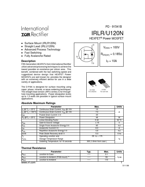
∆V(BR)DSS/∆TJ
Parameter Drain-to-Source Breakdown Voltage Breakdown Voltage Temp. Coefficient Static Drain-to-Source On-Resistance Gate Threshold Voltage Forward Transconductance Drain-to-Source Leakage Current Gate-to-Source Forward Leakage Gate-to-Source Reverse Leakage Total Gate Charge Gate-to-Source Charge Gate-to-Drain ("Miller") Charge Turn-On Delay Time Rise Time Turn-Off Delay Time Fall Time Internal Drain Inductance Internal Source Inductance Input Capacitance Output Capacitance Reverse Transfer Capacitance
10
100
A
100
V D S , D rain-to-S ource V oltage (V )
V D S , D rain-to-S ource V oltage (V )
Fig 1. Typical Output Characteristics
Fig 2. Typical Output Characteristics
** When mounted on 1" square PCB (FR-4 or G-10 Material ) . For recommended footprint and soldering techniques refer to application note #AN-994
ATTINY24A中文资料
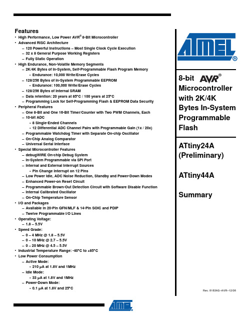
Features•High Performance, Low Power AVR® 8-Bit Microcontroller•Advanced RISC Architecture–120 Powerful Instructions – Most Single Clock Cycle Execution–32 x 8 General Purpose Working Registers–Fully Static Operation•High Endurance, Non-Volatile Memory Segments–2K/4K Bytes of In-System, Self-Programmable Flash Program Memory•Endurance: 10,000 Write/Erase Cycles–128/256 Bytes of In-System Programmable EEPROM•Endurance: 100,000 Write/Erase Cycles–128/256 Bytes of Internal SRAM–Data retention: 20 years at 85°C / 100 years at 25°C–Programming Lock for Self-Programming Flash & EEPROM Data Security •Peripheral Features–One 8-Bit and One 16-Bit Timer/Counter with Two PWM Channels, Each–10-bit ADC•8 Single-Ended Channels•12 Differential ADC Channel Pairs with Programmable Gain (1x / 20x)–Programmable Watchdog Timer with Separate On-chip Oscillator–On-Chip Analog Comparator–Universal Serial Interface•Special Microcontroller Features–debugWIRE On-chip Debug System–In-System Programmable via SPI Port–Internal and External Interrupt Sources•Pin Change Interrupt on 12 Pins–Low Power Idle, ADC Noise Reduction, Standby and Power-Down Modes –Enhanced Power-on Reset Circuit–Programmable Brown-Out Detection Circuit with Software Disable Function –Internal Calibrated Oscillator–On-Chip Temperature Sensor•I/O and Packages–Available in 20-Pin QFN/MLF & 14-Pin SOIC and PDIP–Twelve Programmable I/O Lines•Operating Voltage:–1.8 – 5.5V•Speed Grade:–0 – 4 MHz @ 1.8 – 5.5V–0 – 10 MHz @ 2.7 – 5.5V–0 – 20 MHz @ 4.5 – 5.5V•Industrial Temperature Range: -40°C to +85°C•Low Power Consumption–Active Mode:•210 µA at 1.8V and 1MHz–Idle Mode:•33 µA at 1.8V and 1MHz–Power-Down Mode:•0.1 µA at 1.8V and 25°C 8-bit Microcontrollerwith 2K/4KBytes In-System ProgrammableATtiny24A (Preliminary)ATtiny44A28183AS–AVR–12/08ATtiny24A/44A1.Pin ConfigurationsFigure 1-1.Pinout of ATtiny24A/44A1.1Pin Descriptions1.1.1VCCSupply voltage.1.1.2GNDGround.1.1.3Port B (PB3...PB0)Port B is a 4-bit bi-directional I/O port with internal pull-up resistors (selected for each bit). The Port B output buffers have symmetrical drive characteristics with both high sink and source RESET pin, program (‘0’) RSTDISBL fuse. As inputs, Port B pins that are externally pulled low will source current if the pull-up resistors are activated. The Port B pins are tri-stated when a reset condition becomes active, even if the clock is not running.1234567141312111098VCC(PCINT 8/XT AL1/CLKI) PB0(PCINT9/XTAL2) PB1(PCINT11/RE S ET/dW) PB 3(PCINT10/INT0/OC0A/CKOUT) PB2(PCINT7/ICP/OC0B/ADC7) PA7(PCINT6/OC1A/S DA/MO S I/DI/ADC6) PA6GNDPA0 (ADC0/AREF/PCINT0)PA1 (ADC1/AIN0/PCINT1)PA2 (ADC2/AIN1/PCINT2)PA 3 (ADC 3/T0/PCINT 3)PA4 (ADC4/U S CK/S CL/T1/PCINT4)P A5 (ADC5/DO/MI S O/OC1B/PCINT5)PDIP/S OIC12345QFN/MLF15141312112019181716678910NOTEBottom p a d s ho u ld b e s oldered to gro u nd.DNC: Do Not ConnectD N C D N C G N D V C C D N CPA7 (PCINT7/ICP/OC0B/ADC7)PB2 (PCINT10/INT0/OC0A/CKOUT)PB 3 (PCINT11/RE S ET/dW)PB1 (PCINT9/XTAL2)PB0 (PCINT 8/XTAL1/CLKI)P A 5D N C D N C D N C P A 6Pin 16: P A6 (PCINT6/OC1A/S DA/MO S I/DI/ADC6)Pin 20: P A5 (ADC5/DO/MI S O/OC1B/PCINT5)(ADC4/U S CK/S CL/T1/PCINT4) PA4(ADC 3/T0/PCINT 3) PA 3(ADC2/AIN1/PCINT2) PA2(ADC1/AIN0/PCINT1) PA1(ADC0/AREF/PCINT0) PA038183AS–AVR–12/08ATtiny24A/44APort B also serves the functions of various special features of the ATtiny24A/44A as listed in Section 10.2 “Alternate Port Functions” on page 57.Reset input. A low level on this pin for longer than the minimum pulse length will generate a reset, even if the clock is not running and provided the reset pin has not been disabled. The min-imum pulse length is given in Table 20-4 on page 176. Shorter pulses are not guaranteed to generate a reset.The reset pin can also be used as a (weak) I/O pin.1.1.5Port A (PA7...PA0)Port A is a 8-bit bi-directional I/O port with internal pull-up resistors (selected for each bit). The Port A output buffers have symmetrical drive characteristics with both high sink and source capability. As inputs, Port A pins that are externally pulled low will source current if the pull-up resistors are activated. The Port A pins are tri-stated when a reset condition becomes active,even if the clock is not running.Port A has alternate functions as analog inputs for the ADC, analog comparator, timer/counter,SPI and pin change interrupt as described in “Alternate Port Functions” on page 57.48183AS–AVR–12/08ATtiny24A/44A2.OverviewATtiny24A/44A are low-power CMOS 8-bit microcontrollers based on the AVR enhanced RISC architecture. By executing powerful instructions in a single clock cycle, the ATtiny24A/44A achieves throughputs approaching 1 MIPS per MHz allowing the system designer to optimize power consumption versus processing speed.Figure 2-1.Block DiagramThe AVR core combines a rich instruction set with 32 general purpose working registers. All 32registers are directly connected to the Arithmetic Logic Unit (ALU), allowing two independent registers to be accessed in one single instruction executed in one clock cycle. The resulting architecture is more code efficient while achieving throughputs up to ten times faster than con-ventional CISC microcontrollers.58183AS–AVR–12/08ATtiny24A/44AThe ATtiny24A/44A provides the following features: 2K/4K byte of In-System Programmable Flash, 128/256 bytes EEPROM, 128/256 bytes SRAM, 12 general purpose I/O lines, 32 general purpose working registers, an 8-bit Timer/Counter with two PWM channels, a 16-bit timer/coun-ter with two PWM channels, Internal and External Interrupts, a 8-channel 10-bit ADC,programmable gain stage (1x, 20x) for 12 differential ADC channel pairs, a programmable Watchdog Timer with internal oscillator, internal calibrated oscillator, and four software select-able power saving modes. Idle mode stops the CPU while allowing the SRAM, Timer/Counter,ADC, Analog Comparator, and Interrupt system to continue functioning. ADC Noise Reduction mode minimizes switching noise during ADC conversions by stopping the CPU and all I/O mod-ules except the ADC. In Power-down mode registers keep their contents and all chip functions are disbaled until the next interrupt or hardware reset. In Standby mode, the crystal/resonator oscillator is running while the rest of the device is sleeping, allowing very fast start-up combined with low power consumption.The device is manufactured using Atmel’s high density non-volatile memory technology. The on-chip ISP Flash allows the Program memory to be re-programmed in-system through an SPI serial interface, by a conventional non-volatile memory programmer or by an on-chip boot code running on the AVR core.The ATtiny24A/44A AVR is supported with a full suite of program and system development tools including: C Compilers, Macro Assemblers, Program Debugger/Simulators and Evaluation kits.68183AS–AVR–12/08ATtiny24A/44A3.About3.1ResourcesA comprehensive set of drivers, application notes, data sheets and descriptions on development tools are available for download at /avr.3.2Code ExamplesThis documentation contains simple code examples that briefly show how to use various parts of the device. These code examples assume that the part specific header file is included before compilation. Be aware that not all C compiler vendors include bit definitions in the header files and interrupt handling in C is compiler dependent. Please confirm with the C compiler documen-tation for more details.For I/O Registers located in the extended I/O map, “IN”, “OUT”, “SBIS”, “SBIC”, “CBI”, and “SBI”instructions must be replaced with instructions that allow access to extended I/O. Typically, this means “LDS” and “STS” combined with “SBRS”, “SBRC”, “SBR”, and “CBR”. Note that not all AVR devices include an extended I/O map.3.3Data RetentionReliability Qualification results show that the projected data retention failure rate is much less than 1 PPM over 20 years at 85°C or 100 years at 25°C.3.4DisclaimerTypical values contained in this datasheet are based on simulations and characterization of other AVR microcontrollers manufactured on the same process technology. Min and Max values will be available after the device has been characterized.78183AS–AVR–12/08ATtiny24A/44A4.Register SummaryAddressNameBit 7Bit 6Bit 5Bit 4Bit 3Bit 2Bit 1Bit 0Page0x3F (0x5F)SREG I T H S V N Z C Page 80x3E (0x5E)SPH ––––––SP9SP8Page 100x3D (0x5D)SPL SP7SP6SP5SP4SP3SP2SP1SP0Page 100x3C (0x5C)OCR0B Timer/Counter0 – Output Compare Register B Page 830x3B (0x5B)GIMSK –INT0PCIE1PCIE0––––Page 490x3A (0x5A GIFR –INTF0PCIF1PCIF0––––Page 500x39 (0x59)TIMSK0–––––OCIE0B OCIE0A TOIE0Page 830x38 (0x58)TIFR0––––OCF0BOCF0A TOV0Page 830x37 (0x57)SPMCSR ––RSIG CTPB RFLB PGWRTPGERS SPMEN Page 1560x36 (0x56)OCR0A Timer/Counter0 – Output Compare Register A Page 820x35 (0x55)MCUCR BODS PUD SE SM1SM0BODSE ISC01ISC00Pages 35, 49, and 650x34 (0x54)MCUSR ––––WDRF BORF EXTRF PORF Page 430x33 (0x53)TCCR0B FOC0A FOC0B ––WGM02CS02CS01CS00Page 810x32 (0x52)TCNT0Timer/Counter0Page 820x31(0x51)OSCCAL CAL7CAL6CAL5CAL4CAL3CAL2CAL1CAL0Page290x30 (0x50)TCCR0A COM0A1COM0A0COM0B1COM0B0–WGM01WGM00Page 780x2F (0x4F)TCCR1A COM1A1COM1A0COM1B1COM1B0–WGM11WGM10Page 1060x2E (0x4E)TCCR1B ICNC1ICES1–WGM13WGM12CS12CS11CS10Page 1080x2D (0x4D)TCNT1H Timer/Counter1 – Counter Register High Byte Page 1100x2C (0x4C)TCNT1L Timer/Counter1 – Counter Register Low Byte Page 1100x2B (0x4B)OCR1AH Timer/Counter1 – Compare Register A High Byte Page 1100x2A (0x4A)OCR1AL Timer/Counter1 – Compare Register A Low Byte Page 1100x29 (0x49)OCR1BH Timer/Counter1 – Compare Register B High Byte Page 1100x28 (0x48)OCR1BL Timer/Counter1 – Compare Register B Low BytePage 1100x27 (0x47)DWDR DWDR[7:0]Page 1510x26 (0x46)CLKPR CLKPCE–––CLKPS3CLKPS2CLKPS1CLKPS0Page 300x25 (0x45)ICR1H Timer/Counter1 - Input Capture Register High Byte Page 1110x24 (0x44)ICR1L Timer/Counter1 - Input Capture Register Low BytePage 1110x23 (0x43)GTCCR TSM ––––––PSR10Page 1140x22 (0x42)TCCR1C FOC1A FOC1B ––––––Page 1090x21 (0x41)WDTCSR WDIF WDIE WDP3WDCE WDE WDP2WDP1WDP0Page 430x20 (0x40)PCMSK1––––PCINT11PCINT10PCINT9PCINT8Page 500x1F (0x3F)Reserved ––––––––0x1E (0x3E)EEARL EEAR7EEAR6EEAR5EEAR4EEAR3EEAR2EEAR1EEAR0Page 200x1D (0x3D)EEDR EEPROM Data RegisterPage 210x1C (0x3C)EECR ––EEPM1EEPM0EERIE EEMPE EEPE EERE Page 210x1B (0x3B)PORTA PORTA7PORTA6PORTA5PORTA4PORTA3PORTA2PORTA1PORTA0Page 650x1A (0x3A)DDRA DDA7DDA6DDA5DDA4DDA3DDA2DDA1DDA0Page 650x19 (0x39)PINA PINA7PINA6PINA5PINA4PINA3PINA2PINA1PINA0Page 660x18 (0x38)PORTB ––––PORTB3PORTB2PORTB1PORTB0Page 660x17 (0x37)DDRB ––––DDB3DDB2DDB1DDB0Page 660x16 (0x36)PINB ––––PINB3PINB2PINB1PINB0Page 660x15 (0x35)GPIOR2General Purpose I/O Register 2Page 220x14 (0x34)GPIOR1General Purpose I/O Register 1Page 220x13 (0x33)GPIOR0General Purpose I/O Register 0Page 220x12 (0x32)PCMSK0PCINT7PCINT6PCINT5PCINT4PCINT3PCINT2PCINT1PCINT0Page 510x11 (0x31))Reserved –0x10 (0x30)USIBR USI Buffer Register Page 1270x0F (0x2F)USIDR USI Data RegisterPage 1230x0E (0x2E)USISR USISIF USIOIF USIPF USIDC USICNT3USICNT2USICNT1USICNT0Page 1280x0D (0x2D)USICR USISIE USIOIE USIWM1USIWM0USICS1USICS0USICLK USITC Page 1280x0C (0x2C)TIMSK1––ICIE1––OCIE1B OCIE1A TOIE1Page 1110x0B (0x2B)TIFR1––ICF1––OCF1BOCF1ATOV1Page 1120x0A (0x2A)Reserved –0x09 (0x29)Reserved –0x08 (0x28)ACSR ACD ACBG ACO ACI ACIE ACIC ACIS1ACIS0Page 1290x07 (0x27)ADMUX REFS1REFS0MUX5MUX4MUX3MUX2MUX1MUX0Page 1440x06 (0x26)ADCSRA ADENADSCADATEADIFADIEADPS2ADPS1ADPS0Page 1460x05 (0x25)ADCH ADC Data Register High Byte Page 1480x04 (0x24)ADCL ADC Data Register Low BytePage 1480x03 (0x23)ADCSRB BIN ACME –ADLAR–ADTS2ADTS1ADTS0Page 130, Page 1480x02 (0x22)Reserved –0x01 (0x21)DIDR0ADC7D ADC6D ADC5D ADC4D ADC3D ADC2D ADC1D ADC0D Page 131, Page 1490x00 (0x20)PRR––––PRTIM1PRTIM0PRUSIPRADCPage 3688183AS–AVR–12/08ATtiny24A/44ANote:1.For compatibility with future devices, reserved bits should be written to zero if accessed. Reserved I/O memory addressesshould never be written.2.I/O Registers within the address range 0x00 - 0x1F are directly bit-accessible using the SBI and CBI instructions. In theseregisters, the value of single bits can be checked by using the SBIS and SBIC instructions.3.Some of the Status Flags are cleared by writing a logical one to them. Note that, unlike most other AVRs, the CBI and SBIinstructions will only operation the specified bit, and can therefore be used on registers containing such Status Flags. The CBI and SBI instructions work with registers 0x00 to 0x1F only.98183AS–AVR–12/08ATtiny24A/44A5.Instruction Set SummaryMnemonicsOperandsDescriptionOperation Flags#ClocksARITHMETIC AND LOGIC INSTRUCTIONSADD Rd, Rr Add two RegistersRd ← Rd + RrZ,C,N,V,H 1ADC Rd, Rr Add with Carry two Registers Rd ← Rd + Rr + C Z,C,N,V,H 1ADIW Rdl,K Add Immediate to Word Rdh:Rdl ← Rdh:Rdl + K Z,C,N,V,S 2SUB Rd, Rr Subtract two RegistersRd ← Rd - Rr Z,C,N,V,H 1SUBI Rd, K Subtract Constant from Register Rd ← Rd - K Z,C,N,V,H 1SBC Rd, Rr Subtract with Carry two Registers Rd ← Rd - Rr - C Z,C,N,V,H 1SBCI Rd, K Subtract with Carry Constant from Reg.Rd ← Rd - K - C Z,C,N,V,H 1SBIW Rdl,K Subtract Immediate from Word Rdh:Rdl ← Rdh:Rdl - K Z,C,N,V,S 2AND Rd, Rr Logical AND RegistersRd ← Rd • Rr Z,N,V 1ANDI Rd, K Logical AND Register and Constant Rd ← Rd • K Z,N,V 1OR Rd, Rr Logical OR RegistersRd ← Rd v Rr Z,N,V 1ORI Rd, K Logical OR Register and Constant Rd ← Rd v K Z,N,V 1EOR Rd, Rr Exclusive OR Registers Rd ← Rd ⊕ Rr Z,N,V 1COM Rd One’s Complement Rd ← 0xFF − Rd Z,C,N,V 1NEG Rd Two’s Complement Rd ← 0x00 − Rd Z,C,N,V,H 1SBR Rd,K Set Bit(s) in Register Rd ← Rd v KZ,N,V 1CBR Rd,K Clear Bit(s) in Register Rd ← Rd • (0xFF - K)Z,N,V 1INC Rd Increment Rd ← Rd + 1Z,N,V 1DEC Rd DecrementRd ← Rd − 1 Z,N,V 1TST Rd Test for Zero or Minus Rd ← Rd • Rd Z,N,V 1CLR Rd Clear Register Rd ← Rd ⊕ Rd Z,N,V 1SER Rd Set Register Rd ← 0xFF None 1BRANCH INSTRUCTIONSRJMP kRelative Jump PC ← PC + k + 1None 2IJMP Indirect Jump to (Z)PC ← Z None 2RCALL kRelative Subroutine Call PC ← PC + k + 1None 3ICALL Indirect Call to (Z)PC ←Z None 3RET Subroutine Return PC ← STACK None 4RETI Interrupt Return PC ← STACKI 4CPSE Rd,Rr Compare, Skip if Equal if (Rd = Rr) PC ← PC + 2 or 3None 1/2/3CP Rd,Rr CompareRd − Rr Z, N,V,C,H 1 CPC Rd,Rr Compare with CarryRd − Rr − C Z, N,V,C,H 1CPI Rd,K Compare Register with Immediate Rd − KZ, N,V,C,H 1SBRC Rr, b Skip if Bit in Register Cleared if (Rr(b)=0) PC ← PC + 2 or 3 None 1/2/3SBRS Rr, b Skip if Bit in Register is Set if (Rr(b)=1) PC ← PC + 2 or 3None 1/2/3SBIC P, b Skip if Bit in I/O Register Cleared if (P(b)=0) PC ← PC + 2 or 3 None 1/2/3SBIS P, b Skip if Bit in I/O Register is Set if (P(b)=1) PC ← PC + 2 or 3None 1/2/3BRBS s, k Branch if Status Flag Set if (SREG(s) = 1) then PC ←PC+k + 1None 1/2BRBC s, k Branch if Status Flag Cleared if (SREG(s) = 0) then PC ←PC+k + 1None 1/2BREQ k Branch if Equal if (Z = 1) then PC ← PC + k + 1None 1/2BRNE k Branch if Not Equal if (Z = 0) then PC ← PC + k + 1None 1/2BRCS k Branch if Carry Set if (C = 1) then PC ← PC + k + 1None 1/2BRCC k Branch if Carry Cleared if (C = 0) then PC ← PC + k + 1None 1/2BRSH k Branch if Same or Higher if (C = 0) then PC ← PC + k + 1None 1/2BRLO k Branch if Lower if (C = 1) then PC ← PC + k + 1None 1/2BRMI k Branch if Minus if (N = 1) then PC ← PC + k + 1None 1/2BRPL k Branch if Plusif (N = 0) then PC ← PC + k + 1None 1/2BRGE k Branch if Greater or Equal, Signed if (N ⊕ V= 0) then PC ← PC + k + 1None 1/2BRLT k Branch if Less Than Zero, Signed if (N ⊕ V= 1) then PC ← PC + k + 1None 1/2BRHS k Branch if Half Carry Flag Set if (H = 1) then PC ← PC + k + 1None 1/2BRHC k Branch if Half Carry Flag Cleared if (H = 0) then PC ← PC + k + 1None 1/2BRTS k Branch if T Flag Set if (T = 1) then PC ← PC + k + 1None 1/2BRTC k Branch if T Flag Cleared if (T = 0) then PC ← PC + k + 1None 1/2BRVS k Branch if Overflow Flag is Set if (V = 1) then PC ← PC + k + 1None 1/2BRVC k Branch if Overflow Flag is Cleared if (V = 0) then PC ← PC + k + 1None 1/2BRIE k Branch if Interrupt Enabled if ( I = 1) then PC ← PC + k + 1None 1/2BRID k Branch if Interrupt Disabled if ( I = 0) then PC ← PC + k + 1None 1/2BIT AND BIT-TEST INSTRUCTIONSSBI P,b Set Bit in I/O Register I/O(P,b) ←1None 2CBI P,b Clear Bit in I/O Register I/O(P,b) ← 0None 2LSL Rd Logical Shift Left Rd(n+1) ← Rd(n), Rd(0) ← 0Z,C,N,V 1LSR Rd Logical Shift Right Rd(n) ← Rd(n+1), Rd(7) ← 0Z,C,N,V 1ROLRd Rotate Left Through CarryRd(0)←C,Rd(n+1)← Rd(n),C ←Rd(7)Z,C,N,V1108183AS–AVR–12/08ATtiny24A/44AROR Rd Rotate Right Through CarryRd(7)←C,Rd(n)← Rd(n+1),C ←Rd(0)Z,C,N,V 1ASR Rd Arithmetic Shift Right Rd(n) ← Rd(n+1), n=0..6Z,C,N,V 1SWAP Rd Swap Nibbles Rd(3..0)←Rd(7..4),Rd(7..4)←Rd(3..0)None 1BSET s Flag Set SREG(s) ← 1SREG(s)1BCLR s Flag ClearSREG(s) ← 0 SREG(s)1BST Rr, b Bit Store from Register to T T ← Rr(b)T 1BLD Rd, bBit load from T to Register Rd(b) ← T None 1SEC Set Carry C ←1C 1CLC Clear Carry C ← 0 C 1SEN Set Negative Flag N ←1N 1CLN Clear Negative Flag N ← 0 N 1SEZ Set Zero Flag Z ← 1Z 1CLZ Clear Zero Flag Z ← 0 Z 1SEI Global Interrupt Enable I ←1I 1CLI Global Interrupt Disable I ← 0 I 1SES Set Signed Test Flag S ← 1S 1CLS Clear Signed Test FlagS ← 0 S 1SEV Set Twos Complement Overflow.V ← 1V 1CLV Clear Twos Complement Overflow V ← 0 V 1SET Set T in SREG T ←1T 1CLT Clear T in SREGT ← 0T 1SEH Set Half Carry Flag in SREGH ←1H 1CLHClear Half Carry Flag in SREGH ← 0H 1DATA TRANSFER INSTRUCTIONS MOV Rd, Rr Move Between RegistersRd ← Rr None 1MOVW Rd, Rr Copy Register Word Rd+1:Rd ← Rr+1:Rr None 1LDI Rd, K Load Immediate Rd ← KNone 1LD Rd, X Load Indirect Rd ← (X)None 2LD Rd, X+Load Indirect and Post-Inc.Rd ← (X), X ← X + 1None 2LD Rd, - X Load Indirect and Pre-Dec.X ← X - 1, Rd ← (X)None 2LD Rd, Y Load IndirectRd ← (Y)None 2LD Rd, Y+Load Indirect and Post-Inc.Rd ← (Y), Y ← Y + 1None 2LD Rd, - Y Load Indirect and Pre-Dec.Y ← Y - 1, Rd ← (Y)None 2LDD Rd,Y+q Load Indirect with Displacement Rd ← (Y + q)None 2LD Rd, Z Load Indirect Rd ← (Z)None 2LD Rd, Z+Load Indirect and Post-Inc.Rd ← (Z), Z ← Z+1None 2LD Rd, -Z Load Indirect and Pre-Dec.Z ← Z - 1, Rd ← (Z)None 2LDD Rd, Z+q Load Indirect with Displacement Rd ← (Z + q)None 2LDS Rd, k Load Direct from SRAM Rd ← (k)None 2ST X, Rr Store Indirect(X) ← RrNone 2ST X+, Rr Store Indirect and Post-Inc.(X) ← Rr, X ← X + 1None 2ST - X, Rr Store Indirect and Pre-Dec.X ← X - 1, (X) ← Rr None 2ST Y, Rr Store Indirect(Y) ← RrNone 2ST Y+, Rr Store Indirect and Post-Inc.(Y) ← Rr, Y ← Y + 1None 2ST - Y, Rr Store Indirect and Pre-Dec.Y ← Y - 1, (Y) ← Rr None 2STD Y+q,Rr Store Indirect with Displacement (Y + q) ← Rr None 2ST Z, Rr Store Indirect(Z) ← RrNone 2ST Z+, Rr Store Indirect and Post-Inc.(Z) ← Rr, Z ← Z + 1None 2ST -Z, Rr Store Indirect and Pre-Dec.Z ← Z - 1, (Z) ← Rr None 2STD Z+q,Rr Store Indirect with Displacement (Z + q) ← Rr None 2STS k, RrStore Direct to SRAM (k) ← Rr None 2LPM Load Program Memory R0 ← (Z)None 3LPM Rd, Z Load Program MemoryRd ← (Z)None 3LPM Rd, Z+Load Program Memory and Post-Inc Rd ← (Z), Z ← Z+1None 3SPM Store Program Memory (z) ← R1:R0None IN Rd, P In Port Rd ←P None 1OUT P, Rr Out PortP ← Rr None 1PUSH Rr Push Register on Stack STACK ← Rr None 2POP Rd Pop Register from Stack Rd ← STACKNone 2MCU CONTROL INSTRUCTIONSNOP No Operation None1SLEEP Sleep(see specific descr. for Sleep function)None 1WDR Watchdog Reset (see specific descr. for WDR/Timer)None 1BREAKBreakFor On-chip Debug Only NoneN/AMnemonicsOperandsDescriptionOperationFlags#Clocks118183AS–AVR–12/08ATtiny24A/44A6.Ordering InformationNotes:1.This device can also be supplied in wafer form. Please contact your local Atmel sales office for detailed ordering informationand minimum quantities.2.Pb-free packaging, complies to the European Directive for Restriction of Hazardous Substances (RoHS directive). AlsoHalide free and fully Green.6.1ATtiny24ASpeed (MHz)Power SupplyOrdering Code (1)Package (2)Operational Range 201.8 - 5.5VA Ttiny24A-SSU A Ttiny24A-PU A Ttiny24A-MU A Ttiny24A-MMH14S114P320M120M2Industrial (-40°C to 85°C)Package Type14S114-lead, 0.150" Wide Body, Plastic Gull Wing Small Outline Package (SOIC)14P314-lead, 0.300" Wide, Plastic Dual Inline Package (PDIP)20M120-pad, 4 x 4 x 0.8 mm Body, Quad Flat No Lead / Micro Lead Frame Package (QFN/MLF)20M220-pad, 3 x 3 x 0.85 mm Body, Very Thin Quad Flat No Lead Package (VQFN)128183AS–AVR–12/08ATtiny24A/44ANotes:1.This device can also be supplied in wafer form. Please contact your local Atmel sales office for detailed ordering informationand minimum quantities.2.Pb-free packaging, complies to the European Directive for Restriction of Hazardous Substances (RoHS directive). AlsoHalide free and fully Green.6.2ATtiny44ASpeed (MHz)Power SupplyOrdering Code (1)Package (2)Operational Range 201.8 - 5.5VA Ttiny44A-SSU A Ttiny44A-PU A Ttiny44A-MU A Ttiny44A-MMH14S114P320M120M2Industrial (-40°C to 85°C)Package Type14S114-lead, 0.150" Wide Body, Plastic Gull Wing Small Outline Package (SOIC)14P314-lead, 0.300" Wide, Plastic Dual Inline Package (PDIP)20M120-pad, 4 x 4 x 0.8 mm Body, Quad Flat No-Lead/Micro Lead Frame Package (QFN/MLF)20M220-pad, 3 x 3 x 0.85 mm Body, Very Thin Quad Flat No Lead Package (VQFN)138183AS–AVR–12/08ATtiny24A/44A7.Packaging Information7.120M1148183AS–AVR–12/08ATtiny24A/44A7.220M2158183AS–AVR–12/08ATtiny24A/44A7.314P3168183AS–AVR–12/08ATtiny24A/44A7.414S1178183AS–AVR–12/08ATtiny24A/44A8.ErrataThe revision letters in this section refer to the revision of the corresponding ATtiny24A/44A device.8.1ATtiny24A8.1.1Rev. GNot sampled.8.1.2Rev. FNot sampled.188183AS–AVR–12/08ATtiny24A/44A8.2ATtiny44A8.2.1Rev. FNo known errata.8.2.2Rev. ENot sampled.198183AS–AVR–12/08ATtiny24A/44A9.Datasheet Revision History9.1Rev A. 12/081.Initial revision. Created from document 8006H.2.Updated "Ordering Information" on page 17 and page 18. Pb-plated packages are nolonger offered and there are no separate ordering codes for commercial operation range, the only available option now is industrial. Also, updated some order codes to reflect changes in leadframe composition and added VQFN package option.3.Updated data sheet template.4.Removed all references to 8K device.5.Updated characteristic plots of section “Typical Characteristics”, starting on page 182.6.Added characteristic plots:–“Internal Bandgap Voltage vs. Supply Voltage” on page 202–“Internal Bandgap Voltage vs. Temperature” on page 2027.Updated sections:–“Features” on page 1–“Power Reduction Register” on page 34–“Analog Comparator” on page 128–“Features” on page 132–“Operation” on page 133–“Starting a Conversion” on page 134–“ADC Voltage Reference” on page 139–“Speed Grades” on page 1748.Updated Figures:–“Program Memory Map” on page 15–“Data Memory Map” on page 169.Update Tables:–“Device Signature Bytes” on page 161–“DC Characteristics. T A = -40°C to +85°C” on page 173–“Additional Current Consumption for the different I/O modules (absolute values)” on page 182–“Additional Current Consumption (percentage) in Active and Idle mode” on page 1838183AS–AVR–12/08HeadquartersInternationalAtmel Corporation 2325 Orchard Parkway San Jose, CA 95131USATel: 1(408) 441-0311Fax: 1(408) 487-2600Atmel AsiaUnit 1-5 & 16, 19/FBEA Tower, Millennium City 5418 Kwun Tong Road Kwun Tong, Kowloon Hong KongTel: (852) 2245-6100Fax: (852) 2722-1369Atmel Europe Le Krebs8, Rue Jean-Pierre Timbaud BP 30978054 Saint-Quentin-en-Yvelines Cedex FranceTel: (33) 1-30-60-70-00 Fax: (33) 1-30-60-71-11Atmel Japan9F, Tonetsu Shinkawa Bldg.1-24-8 ShinkawaChuo-ku, Tokyo 104-0033JapanTel: (81) 3-3523-3551Fax: (81) 3-3523-7581Product ContactWeb SiteTechnical Support avr@Sales Contact/contactsLiterature Requests /literatureDisclaimer: The information in this document is provided in connection with Atmel products. No license, express or implied, by estoppel or otherwise,to any intellectual property right is granted by this document or in connection with the sale of Atmel products. EXCEPT AS SET FORTH IN ATMEL ’S TERMS AND CONDI-TIONS OF SALE LOCATED ON ATMEL ’S WEB SITE, ATMEL ASSUMES NO LIABILITY WHATSOEVER AND DISCLAIMS ANY EXPRESS, IMPLIED OR STATUTORY WARRANTY RELATING TO ITS PRODUCTS INCLUDING, BUT NOT LIMITED TO, THE IMPLIED WARRANTY OF MERCHANTABILITY, FITNESS FOR A PARTICULAR PURPOSE, OR NON-INFRINGEMENT. IN NO EVENT SHALL ATMEL BE LIABLE FOR ANY DIRECT, INDIRECT, CONSEQUENTIAL, PUNITIVE, SPECIAL OR INCIDEN-TAL DAMAGES (INCLUDING, WITHOUT LIMITATION, DAMAGES FOR LOSS OF PROFITS, BUSINESS INTERRUPTION, OR LOSS OF INFORMATION) ARISING OUT OF THE USE OR INABILITY TO USE THIS DOCUMENT, EVEN IF ATMEL HAS BEEN ADVISED OF THE POSSIBILITY OF SUCH DAMAGES. Atmel makes no representations or warranties with respect to the accuracy or completeness of the contents of this document and reserves the right to make changes to specifications and product descriptions at any time without notice. Atmel does not make any commitment to update the information contained herein. Unless specifically provided otherwise, Atmel products are not suitable for, and shall not be used in, automotive applications. Atmel’s products are not intended, authorized, or warranted for use as components in applications intended to support or sustain life.© 2008 Atmel Corporation. All rights reserved. Atmel ®, logo and combinations thereof, AVR ® and others are registered trademarks or trade-marks of Atmel Corporation or its subsidiaries. Other terms and product names may be trademarks of others.。
FAW24-2R1中文资料

AC InputSingle Output, General-Purpose UL/CSA/TÜV ApprovedThe F series FAW is characterized by a wide input voltage rangenot requiring switching for connections to input voltages of AC.85to 264V and by the thin type of 25mm in thickness. This series ofpower supplies are UL/CSA/TÜV approved so as to be used withconfidence at the worldwide commercial AC voltages.FEATURES•Thin-type single output power supply with wide input voltagerange (AC.100 to 200V; Switching not required).•Compact open frame type (A cover is available as option).•Full product lineup covering 15W to 150W.•LED indicator display function.•Low noise (FCC class B and VDE class B meet).PART NUMBERS AND RATINGSOutput voltage(V)Current(A)Part No.Current(A)Part No.Current(A)Part No.151FAW15-1R0 1.7FAW15-1R7 3.4FAW15-3R4240.7FAW24-0R7 1.1FAW24-1R1 2.1FAW24-2R1Output voltage(V)520FAW05-20R30FAW05-30R128.3FAW12-8R312FAW12-12R24 4.2FAW24-4R26FAW24-6R0482FAW48-2R0 2.8FAW48-2R8AC InputSingle Output, General-PurposeUL/CSA/TÜV ApprovedFAW15W TYPESPECIFICATIONS AND STANDARDS∗1 Current rating(maximum output current) is determined for 0 to +50°C. Derating is required when used outside this temperature range.∗2 The surge current suppression element is a power thermistor.∗3 Derating is required when the optional cover is attached.Part No.FAW05-3R0FAW12-1R3FAW15-1R0FAW24-0R7Rated output voltage and current∗15V • 3A 12V • 1.3A 15V • 1A 24V • 0.7A Maximum output power W 1515.61516.8Input voltage Eac V 85 to 264[Rating: 100 to 120, 200 to 240]Input frequency Hz 47 to 66[Rating: 50 to 60](Single phase)Input current A 0.4max./0.3max.[AC.100 to 120V/200 to 240V]Fuse rating A 2[Built-in]Surge current ∗2A 22max./34max.[Input and output ratings, 25°C, cold start]Leakage current mA 0.5max./0.75max.[Input and output ratings]Efficiency %70typ.Output characteristics Output voltage Edc V 5121524Voltage variable range Edc V 4.5 to 5.510.8 to 13.213.5 to 16.521.6 to 26.4Maximum output current A 3 1.310.7Overvoltage threshold Edc V 6 to 6.913.7 to 15.717 to 1927 to 30.5Overcurrent threshold A 3.3 to 5.5 1.4 to 2.5 1.1 to 20.8 to 1.4VoltagestabilitySource effect %2max.(1typ.)[Within the input voltage range] Total effect 4max.(2typ.)Load effect %2max.(1typ.)[10 to 100% load]Temperature effect %2max.(1typ.)[Ambient temperature: 0 to +50°C]Drift(Time effect)%0.5max.(0.1typ.)[25°C, input and output ratings, after input voltage ON for 30min to 8h]Recovery %/ms ±4max./2max.[50 to 100% sudden load change]Ripple Ep-p mV 60max.80max.80max.100max.Ripple noise Ep-p mV 120max.190max.220max.310max.Start up time ms 500max.Hold up time ms 15min.Auxiliary functions Indicator display LED(Green) indicates when voltage output is ON.Overvoltage protection Voltage shut-down type, recovers upon reset(interval approx. 30s).Overcurrent protection Rectangular type, automatic recovery.Remote ON-OFF No Remote sensing No Current balance No Safety standards UL1950-3, CSA950-95(C-UL), EN60950(TÜV) approved.Noise terminal voltage FCC class B[AC.100 to 120V], VDE0871 class B[AC.220 to 240V] meet.ConstructionsExternal dimensions mm 25×95×100[H ×W ×L] / With cover(Option)∗3: 30×95×100[H ×W ×L]Weight g 270max.Mounting method Can be attached to 2 sides.Case material Frame: Iron / Cover(Option: 3JC0ZB172-FAW15CA): IronAC InputSingle Output, General-PurposeUL/CSA/TÜV ApprovedFAW15W TYPESHAPES AND DIMENSIONS• Do not insert M3 tap installation screws more than 5mm from the surface of power supply.TERMINAL DESIGNATIONS AND FUNCTIONSTerminal No.Designations and functions 1AC input terminals(L, N)Connect to AC.100 to 120V or AC. 200 to 240V input line.2Frame ground terminal(G)Connect to earth ground. This is connected to the case.4Output voltage adjustment trim Adjusts output voltage.5Operation indicator LEDThis Green LED becomes indicated when voltage is output.AC InputSingle Output, General-PurposeUL/CSA/T ÜV ApprovedFAW25W TYPESPECIFICATIONS AND STANDARDS∗1 Current rating(maximum output current) is determined for 0 to +50°C. Derating is required when used outside this temperature range.∗2 The surge current suppression element is a power thermistor.∗3 Derating is required when the optional cover is attached.Part No.FAW05-5R0FAW12-2R1FAW15-1R7FAW24-1R1Rated output voltage and current∗15V • 5A 12V • 2.1A 15V • 1.7A 24V • 1.1A Maximum output power W 2525.225.526.4Input voltage Eac V 85 to 264[Rating: 100 to 120, 200 to 240]Input frequency Hz 47 to 66[Rating: 50 to 60](Single phase)Input current A 0.7max./0.45max.[AC.100 to 120V/200 to 240V]Fuse rating A 2.5[Built-in]Surge current ∗2A 43max./85max.[Input and output ratings, 25°C, cold start]Leakage current mA 0.5max./0.75max.[Input and output ratings]Efficiency %70typ.Output characteristics Output voltage Edc V 5121524Voltage variable range Edc V 4.5 to 5.510.8 to 13.213.5 to 16.521.6 to 26.4Maximum output current A 5 2.1 1.7 1.1Overvoltage threshold Edc V 6 to 6.913.7 to 15.717 to 1927 to 30.5Overcurrent threshold A 5.5 to 7.5 2.3 to 3.3 1.9 to 2.8 1.2 to 1.8VoltagestabilitySource effect %2max.(1typ.)[Within the input voltage range] Total effect 4max.(2.6typ.)Load effect %2max.(1typ.)[10 to 100% load]Temperature effect %2max.(1typ.)[Ambient temperature: 0 to +50°C]Drift(Time effect)%0.5max.(0.1typ.)[25°C, input and output ratings, after input voltage ON for 30min to 8h]Recovery %/ms ±4max./2max.[50 to 100% sudden load change]Ripple Ep-p mV 80max.100max.120max.150max.Ripple noise Ep-p mV 120max.190max.220max.310max.Start up time ms 500max.Hold up time ms 15min.Auxiliary functions Indicator display LED(Green) indicates when voltage output is ON.Overvoltage protection Voltage shut-down type, recovers upon reset(interval approx. 30s).Overcurrent protection Rectangular type, automatic recovery.Remote ON-OFF No Remote sensing No Current balance No Safety standards UL1950-3, CSA950-95(C-UL), EN60950(T ÜV) approved.Noise terminal voltage FCC class B[AC.100 to 120V], VDE0871 class B[AC.220 to 240V] meet.ConstructionsExternal dimensions mm 25×95×125[H ×W ×L] / With cover(Option)∗3: 30×95×125[H ×W ×L]Weight g 300max.Mounting method Can be attached to 2 sides.Case material Frame: Aluminum / Cover(Option: 3JC0ZB173-FAW25CA): IronAC InputSingle Output, General-PurposeUL/CSA/T ÜV ApprovedFAW25W TYPESHAPES AND DIMENSIONS• Do not insert M3 tap installation screws more than 5mm from the surface of power supply.TERMINAL DESIGNATIONS AND FUNCTIONS1AC input terminals(L, N)Connect to AC.100 to 120V or AC. 200 to 240V input line.2Frame ground terminal(G)Connect to earth ground. This is connected to the case.5Operation indicator LEDThis Green LED becomes indicated when voltage is output.±1mm : without specified dimensionsAC InputSingle Output, General-PurposeUL/CSA/T ÜV ApprovedFAW50W TYPESPECIFICATIONS AND STANDARDS∗1 Current rating(maximum output current) is determined for 0 to +50°C. Derating is required when used outside this temperature range.∗2 The surge current suppression element is a power thermistor.∗3 Derating is required when the optional cover is attached.Part No.FAW05-10R FAW12-4R2FAW15-3R4FAW24-2R1Rated output voltage and current∗15V • 10A 12V • 4.2A 15V • 3.4A 24V • 2.1A Maximum output power W 5050.45150.4Input voltage Eac V 85 to 264[Rating: 100 to 120, 200 to 240]Input frequency Hz 47 to 66[Rating: 50 to 60](Single phase)Input current A 1.2max./0.7max.[AC.100 to 120V/200 to 240V]Fuse rating A 3[Built-in]Surge current ∗2A 45max./90max.[Input and output ratings, 25°C, cold start]Leakage current mA 0.5max./0.75max.[Input and output ratings]Efficiency %76typ.Output characteristics Output voltage Edc V 5121524Voltage variable range Edc V 4.5 to 5.510.8 to 13.213.5 to 16.521.6 to 26.4Maximum output current A 10 4.2 3.4 2.1Overvoltage threshold Edc V 6 to 6.913.7 to 15.717 to 1927 to 30.5Overcurrent threshold A 10.5 to 12 4.4 to 5.1 3.6 to 4.1 2.2 to 2.6VoltagestabilitySource effect %2max.(1typ.)[Within the input voltage range] Total effect 4max.(2typ.)Load effect %2max.(1typ.)[10 to 100% load]Temperature effect %2max.(1typ.)[Ambient temperature: 0 to +50°C]Drift(Time effect)%0.5max.(0.1typ.)[25°C, input and output ratings, after input voltage ON for 30min to 8h]Recovery %/ms ±4max./2max.[50 to 100% sudden load change]Ripple Ep-p mV 80max.100max.120max.150max.Ripple noise Ep-p mV 120max.190max.220max.310max.Start up time ms 500max.Hold up time ms 15min.Auxiliary functions Indicator display LED(Green) indicates when voltage output is ON.Overvoltage protection Voltage shut-down type, recovers upon reset(interval approx. 30s).Overcurrent protection Rectangular type, automatic recovery.Remote ON-OFF No Remote sensing Yes Current balance No Safety standards UL1950-3, CSA950-95(C-UL), EN60950(T ÜV) approved.Noise terminal voltage FCC class B[AC.100 to 120V], VDE0871 class B[AC.220 to 240V] meet.ConstructionsExternal dimensions mm 25×95×165[H ×W ×L] / With cover(Option)∗3: 31×95×165[H ×W ×L] Weight g 450max.Mounting method Can be attached to 2 sides.Case material Frame: Aluminum / Cover(Option: 3JC0ZB174-FAW50CA): IronAC InputSingle Output, General-Purpose UL/CSA/TÜV ApprovedFAW50W TYPESHAPES AND DIMENSIONS• Do not insert M3 tap installation screws more than 5mm from the surface of power supply.TERMINAL DESIGNATIONS AND FUNCTIONSTerminal No.Designations and functions2Frame ground terminal(G)Connect to earth ground. This is connected to the case.3DC output terminals(+, –)Connect to load.6Remote sensing terminals(+S, –S)These terminals are used to compensate voltage loss from the output terminal to a load. Normally they are shorted with a metal bar.AC InputSingle Output, General-PurposeUL/CSA/T ÜV ApprovedFAW100W TYPESPECIFICATIONS AND STANDARDS∗1 Current rating(maximum output current) is determined for 0 to +50°C. Derating is required when used outside this temperature range.∗2 Derating is required when the optional cover is attached.Part No.FAW05-20R FAW12-8R3FAW15-6R6FAW24-4R2FAW48-2R0Rated output voltage and current∗15V • 20A 12V • 8.3A 15V • 6.6A 24V • 4.2A 48V • 2A Maximum output power W 10099.699100.896Input voltage Eac V 85 to 264[Rating: 100 to 120, 200 to 240]Input frequency Hz 47 to 66[Rating: 50 to 60](Single phase)Input current A 2.4max./1.6max.[AC.100 to 120V/200 to 240V]Fuse rating A 5[Built-in]Surge current A 25max./50max.[Input and output ratings, 1st surge current, reset after 30s minimum.]Leakage current mA 0.5max./0.75max.[Input and output ratings]Efficiency %78typ.Output characteristics Output voltage Edc V 512152448Voltage variable range Edc V 4.5 to 5.510.8 to 13.213.5 to 16.521.6 to 26.443.2 to 52.8Maximum output current A 208.3 6.6 4.22Overvoltage threshold Edc V 6 to 6.913.7 to 15.717 to 1927 to 30.553.5 to 60Overcurrent threshold A 21 to 248.7 to 107 to 8 4.4 to 5.2 2.1 to 2.4VoltagestabilitySource effect %2max.(1typ.)[Within the input voltage range] Total effect ±2max.(±1typ.)Load effect %2max.(1typ.)[10 to 100% load]Temperature effect %2max.(1typ.)[Ambient temperature: 0 to +50°C]Drift(Time effect)%0.5max.(0.1typ.)[25°C, input and output ratings, after input voltage ON for 30min to 8h]Recovery %/ms ±4max./1max.[50 to 100% sudden load change]Ripple Ep-p mV 80max.100max.120max.150max.260max.Ripple noise Ep-p mV 120max.190max.220max.310max.530max.Start up time ms 200max.Hold up time ms 15min.Auxiliary functions Indicator display LED(Green) indicates when voltage output is ON.Overvoltage protection Voltage shut-down type, recovers upon reset after roughly 90/120s[AC.120/240V].Overcurrent protection Rectangular type, automatic recovery.Remote ON-OFF No Remote sensing Yes Current balance No Safety standards UL1950-3, CSA950-95(C-UL), EN60950(T ÜV) approved.Noise terminal voltage FCC class B[AC.100 to 120V], VDE0871 class B[AC.220 to 240V] meet.ConstructionsExternal dimensions mm 35×95×200[H ×W ×L] / With cover(Option)∗2: 40×95×200[H ×W ×L]Weight kg 1max.Mounting method Can be attached to 2 sides.Case material Frame: Aluminum / Cover(Option: 2JC0ZG043-FGW100CA): IronAC InputSingle Output, General-Purpose UL/CSA/TÜV ApprovedFAW100W TYPESHAPES AND DIMENSIONS• Do not insert M3 tap installation screws more than 5mm from the surface of power supply.TERMINAL DESIGNATIONS AND FUNCTIONS1AC input terminals(L, N)Connect to AC.100 to 120V or AC. 200 to 240V input line. 2Frame ground terminal(G)Connect to earth ground. This is connected to the case.5Operation indicator LED This Green LED becomes indicated when voltage is output. It is mounted on a miniature base.6Remote sensing terminals(+S, –S)Normally they are shorted with a metal bar.AC InputSingle Output, General-PurposeUL/CSA/T ÜV ApprovedFAW150W TYPESPECIFICATIONS AND STANDARDS∗1 Current rating(maximum output current) is determined for 0 to +50°C. Derating is required when used outside this temperature range.∗2 Derating is required when the optional cover is attached.Part No.FAW05-30R FAW12-12R FAW15-10R FAW24-6R0FAW48-2R8Rated output voltage and current∗15V • 30A 12V • 12A 15V • 10A 24V • 6A 48V • 2.8A Maximum output power W 150144150144134.4Input voltage Eac V 85 to 264[Rating: 100 to 120/200 to 240]Input frequency Hz 47 to 66[Rating: 50 to 60](Single phase)Input current A 3.5max./2max.[AC.100 to 120V/200 to 240V]Fuse rating A 6.3[Built-in]Surge current A 25max./50max.[Input and output ratings, 1st surge current, reset after 30s minimum.]Leakage current mA 0.5max./0.75max.[Input and output ratings]Efficiency %78typ.Output characteristics Output voltage Edc V 512152448Voltage variable range Edc V 4.5 to 5.510.8 to 13.213.5 to 16.521.6 to 26.443.2 to 52.8Maximum output current A 3012106 2.8Overvoltage threshold Edc V 6 to 6.913.7 to 15.717 to 1927 to 30.553.5 to 60Overcurrent threshold A 32 to 3613 to 1511 to 13 6.3 to 7.5 3 to 3.5VoltagestabilitySource effect %2max.(1typ.)[Within the input voltage range] Total effect ±2max.(±1typ.)Load effect %2max.(1typ.)[10 to 100% load]Temperature effect %2max.(1typ.)[Ambient temperature: 0 to +50°C]Drift(Time effect)%0.5max.(0.1typ.)[25°C, input and output ratings, after input voltage ON for 30min to 8h]Recovery %/ms ±4max./1max.[50 to 100% sudden load change]Ripple Ep-p mV 80max.100max.120max.150max.260max.Ripple noise Ep-p mV 120max.190max.220max.310max.530max.Start up time ms 200max.Hold up time ms 15min.Auxiliary functions Indicator display LED(Green) indicates when voltage output is ON.Overvoltage protection Voltage shut-down type, recovers upon reset after roughly 90/120s[AC.120/240V].Overcurrent protection Rectangular type, automatic recovery.Remote ON-OFF No Remote sensing Yes Current balance No Safety standards UL1950-3, CSA950-95(C-UL), EN60950(T ÜV) approved.Noise terminal voltage FCC class B[AC.100 to 120V], VDE0871 class B[AC.220 to 240V] meet.ConstructionsExternal dimensions mm 51×95×200[H ×W ×L] / With cover(Option)∗2: 55×95×200[H ×W ×L]Weight kg 1.2max.Mounting method Can be attached to 2 sides.Case material Frame: Aluminum / Cover(Option: 2JC0ZG044-FGW150CA): IronAC InputSingle Output, General-PurposeUL/CSA/T ÜV ApprovedFAW150W TYPESHAPES AND DIMENSIONS• Do not insert M3 tap installation screws more than 5mm from the surface of power supply.TERMINAL DESIGNATIONS AND FUNCTIONSTerminal No.Designations and functions 1AC input terminals(L, N)Connect to AC.100 to 120V or AC. 200 to 240V input line.4Output voltage adjustment trim Adjusts output voltage.5Operation indicator LEDIt is mounted on a miniature base.6Remote sensing terminals(+S, –S)These terminals are used to compensate voltage loss from the output terminal to a load. Normally they are shorted with a metal bar.7Direct output terminal(+, +, –, –)A use of two pins each is recommended.AC InputSingle Output, General-Purpose UL/CSA/TÜV ApprovedBLOCK DIAGRAM15W AND 25W TYPES50W, 100W AND 150W TYPES∗ The 150W type provides 2 each + and – output terminals.COMMON SPECIFICATIONSTemperature rangeHumidity range20 to 95[Maximum wet-bulb temperature: 35°C, without dewing]VibrationShockWithstand voltage Eac: 2kV, 1min[Normal temperature, normal humidity, cutout current 10mA] Insulation resistance Edc: 500V, 100MΩ min. [Normal temperature, normal humidity]∗ The specifications are intended for a product with a base attached, but not for a product installed with angle bracket.AC InputSingle Output, General-Purpose UL/CSA/TÜV ApprovedOUTPUT POWER-AMBIENT TEMPERATURE(DERATINGS) SURGE CURRENT, START UP / HOLD UP TIMES HANGING INSTALLATION (applicable to 15W, 25W, and 50W types)Recesses are provided at two places on an L-shaped frame. Use them to mount the power supply from its surface.Use the notched and mounting holes for stand-up installation of the power supply.A screwdriver may touch a component on the PC board when rotating the M3 screw.Be careful not to apply any excessive force.AC InputSingle Output, General-Purpose UL/CSA/TÜV ApprovedINSTALLATIONFor natural cooling, apply either of the following installation meth-ods so as to provide a thermal convection:(1) Standard installation(2) Other installations on component surface (upward).In addition, maintain a 15mm min. distance between the compo-nent (cover) surface and surrounding equipment, etc.(1) Standard Installation(1)-1. Angle bracket (downward)(A)(B)•For the installation in (A), arrange a bearer for preventing vibrations on the surface B of the angle bracket or in a direction indicated by an arrow.(2) Other Installations(2)-1. Component surface (upward)(A)(B)•For the installation in (B), arrange a bearer for preventing vibrations on the surface B of the angle bracket or in a direction indicated by an arrow.(2)-2. Component surface (downward)(A)(B)•This type of installation is inhibited due to a difficulty of the thermal convection.(2)-3. Angle bracket (upward)(A)(B)•This type of installation is inhibited due to a difficulty of the thermal convection.COVERThe cover is separately available. Please order it with the follow-ing model names:Type Cover model No.50W3JC0ZB174-FAW50CA 100W2JC0ZG043-FGW100CA。
Z23S2445M01中文资料(AEROVOX)中文数据手册「EasyDatasheet - 矽搜」
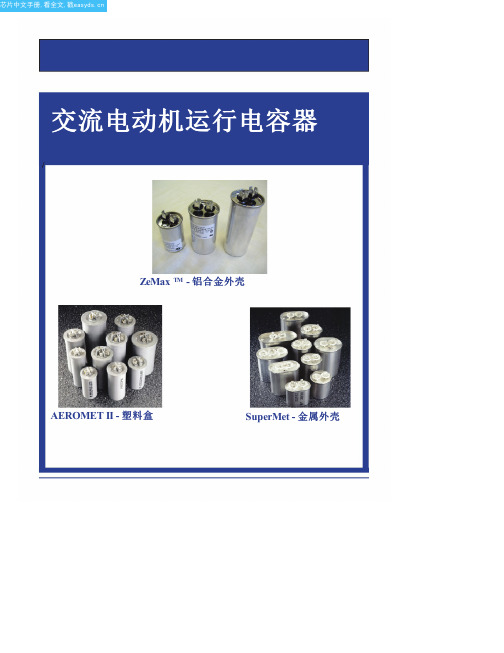
•单和双额定值 - 双额定值
在SuperMet仅
所有SuperMet和ZEMAX电容TM集成•
60000小时使用寿命.
UL认证压敏灭弧删除•
电容稳定性±整个人生3%
电容器从电路在生命尽头.
•自清除金属化聚丙烯薄膜.
• 专利压力灭弧符合UL810
每个电容器填充有环氧化Soybeanoil
要求.
电介液.大豆油已被证明可靠性
所有AEROMET II电容都可以用时间和成本节约
EIA RS-186-3E状态测试要求.
AeroMount系统.触点厂家触点厂家对于需要reycled了解详细信息.
认证证书
EIA RS-186-2E湿度测试要求(TropiCAL条件).
• UL文件号E51176
• CSA文件号058450
• VDE认证可用
电气特性
• 温度范围:-40〜+ 70℃.源自• 电容范围3至80μF.
• 电容公差±10%.
• 电压范围240至480 VAC,60赫兹.
• 损耗因数0.1%以下
@ 60赫兹和25℃.
• 绝缘电阻千M
●μF.
•耐电压.
• 期限至足月1.75×WVAC
• 期限到案2×WVAC + 1KVAC
应用
• 窗式空调 • 单元式空调 • 电动汽车 • 风扇与鼓风机 • Pumps • 洗衣房设备 • 除湿机
注入
P = Supernol(M系列) S = SuperSoy(Z系列)
电压编码 电压第一个两位数
24 = 240 V交流 33 = 330 V交流 37 = 370 V交流 44 = 440 V交流 48 = 480 V交流 60 = 600 Vac
IRLZ24NPBF中文资料
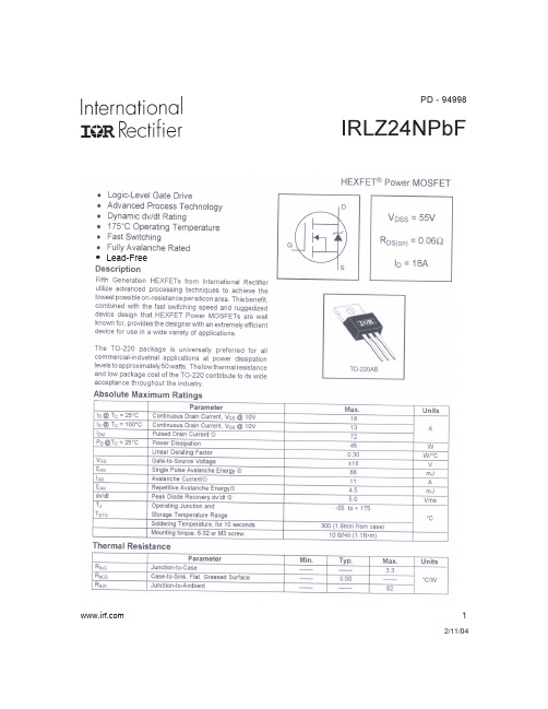
PD - 94998
IRLZ24NPbF
•
Lead-Free
1
2/11/04
元器件交易网
IRLZ24NPbF
2
元器件交易网
IRLZ24NPbF
Dimensions are shown in millimeters (inches)
-B4.69 (.185) 4.20 (.165) 1.32 (.052) 1.22 (.048)
பைடு நூலகம்
4 15.24 (.600) 14.84 (.584)
1.15 (.045) MIN 1 2 3
LEAD ASSIGNMENTS IGBTs, CoPACK 1 - GATE 21- GATE DRAIN 1- GATE 32- DRAINSOURCE 2- COLLECTOR 3- SOURCE 3- EMITTER 4 - DRAIN
3 OUTLINE CONFORMS TO JEDEC OUTLINE TO-220AB. 4 HEATSINK & LEAD MEASUREMENTS DO NOT INCLUDE BURRS.
TO-220AB Part Marking Information
E XAMPL E : T HIS IS AN IR F 1010 LOT CODE 1789 AS S E MB L E D ON WW 19, 1997 IN T H E AS S E MB L Y LINE "C" INT E R NAT IONAL R E CT IF IE R L OGO AS S E MB L Y L OT CODE PAR T NU MB E R
Note: "P" in assembly line position indicates "Lead-Free"
24IMR6-05-2中文资料
15.24 (0.6")
Measuring point of case temperature TC
1
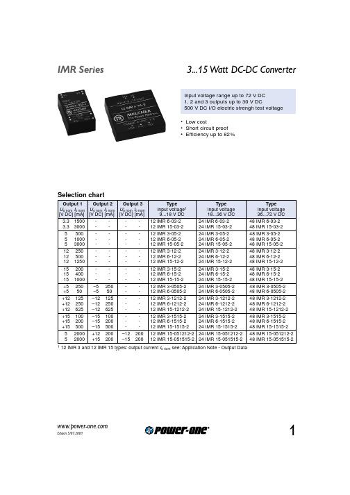
Type Input voltage1 9...18 V DC 12 IMR 6-03-2 12 IMR 15-03-2 12 IMR 3-05-2 12 IMR 6-05-2 12 IMR 15-05-2 12 IMR 3-12-2 12 IMR 6-12-2 12 IMR 15-12-2 12 IMR 3-15-2 12 IMR 6-15-2 12 IMR 15-15-2 12 IMR 3-0505-2 12 IMR 6-0505-2 12 IMR 3-1212-2 12 IMR 6-1212-2 12 IMR 15-1212-2 12 IMR 3-1515-2 12 IMR 6-1515-2 12 IMR 15-1515-2 12 IMR 15-051212-2 12 IMR 15-051515-2
Selection chart
Output 1 Output 2 Output 3 Uo nom Io nom Uo nom Io nom Uo nom Io nom [V DC] [mA] [V DC] [mA] [V DC] [mA] 3.3 1500 3.3 3000 5 500 5 1000 5 3000 12 250 12 500 12 1250 15 200 15 400 15 1000 +5 250 –5 250 +5 50 –5 50 +12 125 –12 125 +12 250 –12 250 +12 625 –12 625 +15 100 –15 100 +15 200 –15 200 +15 500 –15 500 5 2000 +12 200 –12 200 5 2000 +15 200 –15 200
R1224N332H中文资料
Designation of Optional Function E : 300kHz, with a PWM/VFM alternative circuit F : 500kHz, with a PWM/VFM alternative circuit G : 300kHz, without a PWM/VFM alternative circuit H : 500kHz, without a PWM/VFM alternative circuit L : 180kHz, with a PWM/VFM alternative circuit M :180kHz, without a PWM/VFM alternative circuit
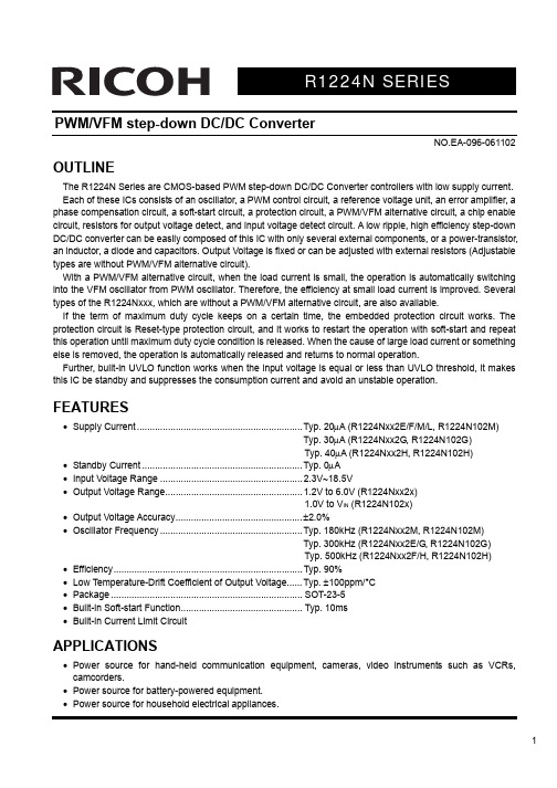
In the R1224N Series, the output voltage, the oscillator frequency, the optional function, and the taping type for the ICs can be selected at the user's request.
The selection can be made with designating the part number as shown below;
R1224Nxx2x-xx-x ←Part Number
↑ ↑ ↑↑ ↑ ↑ a b cd e f
Code a b c
d
e f
Contents
Designation of Package Type; N: SOT-23-5
Typ. 300kHz (R1224Nxx2E/G, R1224N102G) Typ. 500kHz (R1224Nxx2F/H, R1224N102H) • Efficiency......................................................................... Typ. 90% • Low Temperature-Drift Coefficient of Output Voltage...... Typ. ±100ppm/°C • Package .......................................................................... SOT-23-5 • Built-in Soft-start Function............................................... Typ. 10ms • Built-in Current Limit Circuit
IRLZ34N中文资料
Description
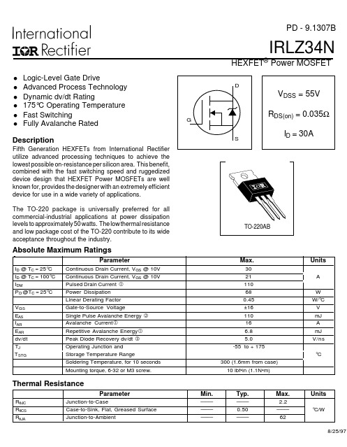
Fifth Generation HEXFETs from International Rectifier utilize advanced processing techniques to achieve the lowest possible on-resistance per silicon area. This benefit, combined with the fast switching speed and ruggedized device design that HEXFET Power MOSFETs are well known for, provides the designer with an extremely efficient device for use in a wide variety of applications.
VGS(th)
Gate Threshold Voltage
1.0 ––– 2.0 V VDS = VGS, ID = 250µA
gfs
Forward Transconductance
11 ––– ––– S VDS = 25V, ID = 16A
IDSS
Drain-to-Source Leakage Current
VGS = 5.0V, See Fig. 6 and 13
td(on)
Turn-On Delay Time
––– 8.9 –––
VDD = 28V
tr td(off)
Rise Time Turn-Off Delay Time
––– 100 ––– ns ID = 16A
––– 21 –––
RG = 6.5Ω, VGS = 5.0V
场效应管

场效应管所属分类:化学半导体半导体器件物理学科学摘要:场效应晶体管(Field Effect Transistor缩写(FET))简称场效应管。
由多数载流子参与导电,也称为单极型晶体管。
它属于电压控制型半导体器件。
具有输入电阻高(108~109Ω)、噪声小、功耗低、动态范围大、易于集成、没有二次击穿现象、安全工作区域宽等优点,现已成为双极型晶体管和功率晶体管的强大竞争者。
提问编辑摘要目录[隐藏]∙ 1 基本特点∙ 2 工作原理∙ 3 主要参数∙ 4 型号命名∙ 5 主要作用∙ 6 试验测试∙7 分类简介∙8 测量方法∙9 判断方法∙10 产品特性∙11 电气特性∙12 特性曲线∙13 参数符号∙14 注意事项∙15 使用优势∙16 应用领域∙17 应用特点∙18 产品展示场效应管-基本特点方型场效应管场效应管属于电压控制元件,这一点类似于电子管的三极管,但它的构造与工作原理和电子管是截然不同的,与双极型晶体管相比,场效应晶体管具有如下特点:(1)场效应管是电压控制器件,它通过UGS来控制ID;(2)场效应管的输入端电流极小,因此它的输入电阻很大。
(3)它是利用多数载流子导电,因此它的温度稳定性较好;(4)它组成的放大电路的电压放大系数要小于三极管组成放大电路的电压放大系数;(5)场效应管的抗辐射能力强;(6)由于不存在杂乱运动的少子扩散引起的散粒噪声,所以噪声低。
场效应管-工作原理场效应管场效应管工作原理用一句话说,就是“漏极-源极间流经沟道的ID,用以门极与沟道间的pn 结形成的反偏的门极电压控制ID”。
更正确地说,ID流经通路的宽度,即沟道截面积,它是由pn结反偏的变化,产生耗尽层扩展变化控制的缘故。
在VGS=0的非饱和区域,表示的过渡层的扩展因为不很大,根据漏极-源极间所加VDS的电场,源极区域的某些电子被漏极拉去,即从漏极向源极有电流ID流动。
从门极向漏极扩展的过度层将沟道的一部分构成堵塞型,ID饱和。
IRFZ24中文资料

60171268±20149174.45.544Value Units A V mJ A mJ V/ns W A V TO-2201.Gate2. Drain3. Source321TRADEMARKSACEx™CoolFET™CROSSVOLT™E 2CMOS TM FACT™FACT Quiet Series™FAST ®FASTr™GTO™HiSeC™The following are registered and unregistered trademarks Fairchild Semiconductor owns or is authorized to use and is not intended to be an exhaustive list of all such trademarks.LIFE SUPPORT POLICYFAIRCHILD’S PRODUCTS ARE NOT AUTHORIZED FOR USE AS CRITICAL COMPONENTS IN LIFE SUPPORTDEVICES OR SYSTEMS WITHOUT THE EXPRESS WRITTEN APPROV AL OF FAIRCHILD SEMICONDUCTOR CORPORA TION.As used herein:ISOPLANAR™MICROWIRE™POP™PowerTrench™QS™Quiet Series™SuperSOT™-3SuperSOT™-6SuperSOT™-8TinyLogic™1. Life support devices or systems are devices or systems which, (a) are intended for surgical implant intothe body, or (b) support or sustain life, or (c) whosefailure to perform when properly used in accordancewith instructions for use provided in the labeling, can be reasonably expected to result in significant injury to the user.2. A critical component is any component of a lifesupport device or system whose failure to perform can be reasonably expected to cause the failure of the life support device or system, or to affect its safety or effectiveness.PRODUCT STATUS DEFINITIONS Definition of TermsDatasheet Identification Product Status Definition Advance InformationPreliminary No Identification Needed Obsolete This datasheet contains the design specifications for product development. Specifications may change in any manner without notice.This datasheet contains preliminary data, andsupplementary data will be published at a later date.Fairchild Semiconductor reserves the right to make changes at any time without notice in order to improve design.This datasheet contains final specifications. Fairchild Semiconductor reserves the right to make changes at any time without notice in order to improve design.This datasheet contains specifications on a product that has been discontinued by Fairchild semiconductor.The datasheet is printed for reference information only.Formative or In DesignFirst ProductionFull ProductionNot In ProductionDISCLAIMERFAIRCHILD SEMICONDUCTOR RESERVES THE RIGHT TO MAKE CHANGES WITHOUT FURTHER NOTICE TO ANY PRODUCTS HEREIN TO IMPROVE RELIABILITY , FUNCTION OR DESIGN. FAIRCHILD DOES NOT ASSUME ANY LIABILITY ARISING OUT OF THE APPLICATION OR USE OF ANY PRODUCT OR CIRCUIT DESCRIBED HEREIN; NEITHER DOES IT CONVEY ANY LICENSE UNDER ITS PATENT RIGHTS, NOR THE RIGHTS OF OTHERS.。
24N60C3中文资料
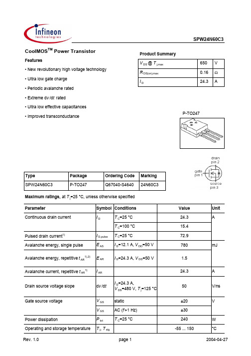
SPW24N60C3Parameter Symbol Conditions Unitmin.typ.max. Thermal characteristicsThermal resistance, junction - case R thJC--0.52K/WR thJA leaded--62Soldering temperature T sold 1.6 mm (0.063 in.)from case for 10 s--260°CElectrical characteristics, at T j=25 °C, unless otherwise specifiedStatic characteristicsDrain-source breakdown voltage V(BR)DSS V GS=0 V, I D=250 µA600--V Avalanche breakdown voltage V(BR)DS V GS=0 V, I D=24.3 A-700-Gate threshold voltage V GS(th)V DS=V GS, I D=1.2 mA 2.13 3.9Zero gate voltage drain current I DSS V DS=600 V, V GS=0 V,T j=25 °C-0.11µAV DS=600 V, V GS=0 V,T j=150 °C--100Gate-source leakage current I GSS V GS=20 V, V DS=0 V--100nADrain-source on-state resistance R DS(on)V GS=10 V, I D=15.4 A,T j=25 °C-0.140.16ΩV GS=10 V, I D=15.4 A,T j=150 °C-0.34-Gate resistance R G f=1 MHz, open drain-0.7-Transconductance g fs |V DS|>2|I D|R DS(on)max,I D=15.4 A-24-SValuesThermal resistance, junction - ambientSPW24N60C3Parameter Symbol Conditions Unitmin.typ.max. Dynamic characteristicsInput capacitance C iss-2800-pF Output capacitance C oss-930-Reverse transfer capacitance C rss-66-Effective output capacitance, energyrelated3)C o(er)-114-Effective output capacitance, timerelated4)C o(tr)-204-Turn-on delay time t d(on)-13-ns Rise time t r-21-Turn-off delay time t d(off)-73-Fall time t f-6-Gate Charge CharacteristicsGate to source charge Q gs-15-nC Gate to drain charge Q gd-49-Gate charge total Q g-105137Gate plateau voltage V plateau- 5.4-V4)Co(tr) is a fixed capacitance that gives the same charging time as C oss while V DS is rising from 0 to 80% V DSS.ValuesV GS=0 V, V DS=25 V,f=1 MHzV DD=480 V,V GS=10 V, I D=24.3 A,R G=3.3 ΩV DD=480 V,I D=24.3 A,V GS=0 to 10 VV GS=0 V, V DS=0 Vto 480 V1) Pulse width limited by maximum temperature Tj,maxonly2) Repetitive avalanche causes additional power losses that can be calculated as PAV=E AR*f.3)Co(er)is a fixed capacitance that gives the same stored energy as C oss while V DS is rising from 0 to 80% V DSS.SPW24N60C3 Definition of diode switching characteristicsP-TO247: OutlineDimensions in mmSPW24N60C3 Published byInfineon Technologies AGBereich KommunikationSt.-Martin-Straße 53D-81541 München© Infineon Technologies AG 1999All Rights Reserved.Attention please!The information herein is given to describe certain components and shall not be considered aswarranted characteristics.Terms of delivery and rights to technical change reserved.We hereby disclaim any and all warranties, including but not limited to warranties of non-infringement, regarding circuits, descriptions and charts stated herein.Infineon Technologies is an approved CECC manufacturer.InformationFor further information on technology, delivery terms and conditions and prices, please contact your nearest Infineon Technologies office in Germany or our Infineon Technologies representatives worldwide (see address list).WarningsDue to technical requirements, components may contain dangerous substances.For information on the types in question, please contact your nearest Infineon Technologies office. Infineon Technologies' components may only be used in life-support devices or systems with the expressed written approval of Infineon Technologies if a failure of such components can reasonablybe expected to cause the failure of that life-support device or system, or to affect the safety or effectiveness of that device or system. Life support devices or systems are intended to be implantedin the human body, or to support and/or maintain and sustain and/or protect human life. If they fail,it is reasonable to assume that the health of the user or other persons may be endangered.。
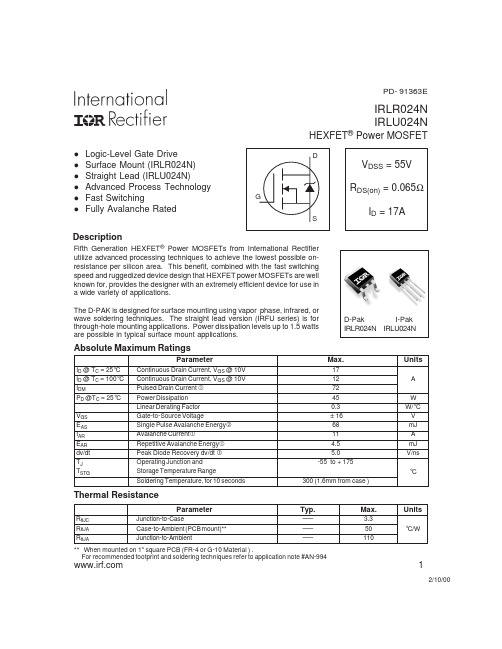
IRLU024N中文资料
HEXFET ®Power MOSFETParameterTyp.Max.UnitsR θJC Junction-to-Case––– 3.3R θJA Case-to-Ambient (PCB mount)**–––50°C/WR θJAJunction-to-Ambient–––110Thermal ResistanceDescription2/10/00 1l Logic-Level Gate Drive l Surface Mount (IRLR024N)l Straight Lead (IRLU024N)l Advanced Process Technology l Fast SwitchinglFully Avalanche RatedFifth Generation HEXFET ® Power MOSFETs from International Rectifier utilize advanced processing techniques to achieve the lowest possible on-resistance per silicon area. This benefit, combined with the fast switching speed and ruggedized device design that HEXFET power MOSFETs are well known for, provides the designer with an extremely efficient device for use in a wide variety of applications.The D-PAK is designed for surface mounting using vapor phase, infrared, or wave soldering techniques. The straight lead version (IRFU series) is for through-hole mounting applications. Power dissipation levels up to 1.5 watts are possible in typical surface mount applications.** When mounted on 1" square PCB (FR-4 or G-10 Material ) .For recommended footprint and soldering techniques refer to application note #AN-994ParameterMax.UnitsI D @ T C = 25°C Continuous Drain Current, V GS @ 10V 17I D @ T C = 100°C Continuous Drain Current, V GS @ 10V 12A I DMPulsed Drain Current 72P D @T C = 25°C Power Dissipation 45W Linear Derating Factor 0.3W/°C V GS Gate-to-Source Voltage± 16V E AS Single Pulse Avalanche Energy 68mJ I AR Avalanche Current11A E AR Repetitive Avalanche Energy 4.5mJ dv/dt Peak Diode Recovery dv/dt 5.0V/ns T J Operating Junction and-55 to + 175T STGStorage Temperature RangeSoldering Temperature, for 10 seconds300 (1.6mm from case )°CAbsolute Maximum RatingsPD- 91363ED-Pak I-Pak IRLR024N IRLU024NIRLR024N IRLU024NIRLR/U024NIRLR/U024NIRLR/U024NIRLR/U024NIRLR/U024NIRLR/U024NIRLR/U024NIRLR/U024NIRLR/U024N。
IRLL024Z中文资料

max. junction temperature. (See fig. 11).
repetitive avalanche performance.
Limited by TJmax, starting TJ = 25°C, L = 4.8mH
This value determined from sample failure population.
Max. 5.0 4.0 40 2.8 1.0 0.02 ± 16 21 38 See Fig.12a, 12b, 15, 16
-55 to + 150
Typ. ––– –––
Max. 45 120
Units
A
W W/°C
V mJ
A mJ
°C Units °C/W
1
08/03/04
3.0V
TOP BOTTOM
VGS 10V 9.0V 7.0V 5.0V 4.5V 4.0V 3.5V 3.0V
0.1 0.1
≤60µs PULSE WIDTH Tj = 150°C
1
10
100
VDS, Drain-to-Source Voltage (V)
Fig 2. Typical Output Characteristics
3.0V 1
0.1 0.1
≤60µs PULSE WIDTH Tj = 25°C
1
10
100
VDS, Drain-to-Source Voltage (V)
Fig 1. Typical Output Characteristics
ID, Drain-to-Source Current (A)
100 10 1
IRLZ24NL中文资料
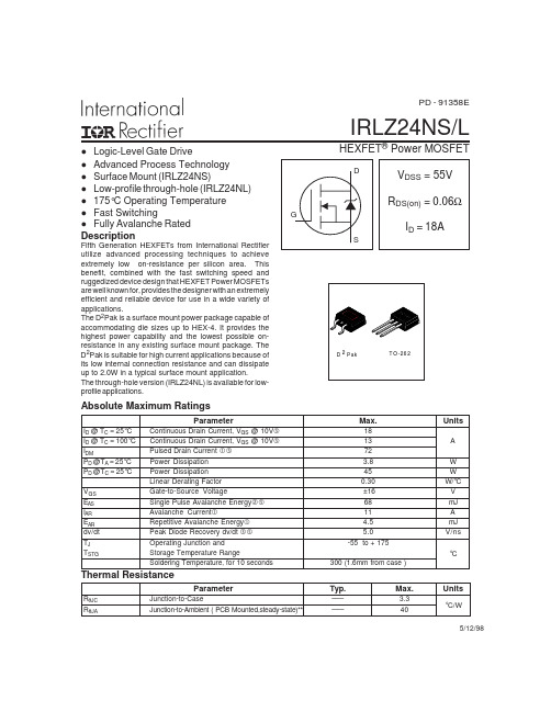
IRLZ24NS/LHEXFET ® Power MOSFETPD - 91358El Advanced Process Technology l Surface Mount (IRLZ24NS)l Low-profile through-hole (IRLZ24NL)l 175°C Operating Temperature l Fast Switchingl Fully Avalanche Rated ParameterTyp.Max.UnitsR θJC Junction-to-Case––– 3.3R θJAJunction-to-Ambient ( PCB Mounted,steady-state)**–––40Thermal Resistance°C/WParameterMax.UnitsI D @ T C = 25°C Continuous Drain Current, V GS @ 10V 18I D @ T C = 100°C Continuous Drain Current, V GS@ 10V 13A I DMPulsed Drain Current 72P D @T A = 25°C Power Dissipation 3.8W P D @T C = 25°C Power Dissipation 45W Linear Derating Factor 0.30W/°C V GS Gate-to-Source Voltage±16V E AS Single Pulse Avalanche Energy 68mJ I AR Avalanche Current11A E AR Repetitive Avalanche Energy 4.5mJ dv/dt Peak Diode Recovery dv/dt 5.0V/ns T J Operating Junction and-55 to + 175T STGStorage Temperature RangeSoldering Temperature, for 10 seconds300 (1.6mm from case )°CAbsolute Maximum RatingsFifth Generation HEXFETs from International Rectifier utilize advanced processing techniques to achieve extremely low on-resistance per silicon area. This benefit, combined with the fast switching speed and ruggedized device design that HEXFET Power MOSFETs are well known for, provides the designer with an extremely efficient and reliable device for use in a wide variety of applications.The D 2Pak is a surface mount power package capable of accommodating die sizes up to HEX-4. It provides the highest power capability and the lowest possible on-resistance in any existing surface mount package. The D 2Pak is suitable for high current applications because of its low internal connection resistance and can dissipate up to 2.0W in a typical surface mount application.The through-hole version (IRLZ24NL) is available for low-profile applications.Description2 D PakT O -2625/12/98lLogic-Level Gate DriveIRLZ24NS/LIRLZ24NS/LIRLZ24NS/LIRLZ24NS/LIRLZ24NS/LIRLZ24NS/LIRLZ24NS/LIRLZ24NS/LIRLZ24NS/L。
nrf24L01中文资料
COPYRIGHT ©2005 ALL RIGHTS RESERVED 迅通科技 TEL:+86 10 64390486 E-mail: sales@
图 4 nRF24L01 在星形网络中的结构图 good,,翻译的很好,,,频道一定是相同的,,,
nRF24L01 在接收模式下可以接收 6 路不同通道的数据 见图 4 每一个数据通道使用不同的地址 但
● 极低的晶振要求
60ppm
● 低成本电感和双面 PCB 板
● 工作电压 1.9~3.6V
应用
● 无线鼠标 键盘 ● 无线门禁 ● 无线数据通讯 ● 安防系统 ● 遥控装置 ● 遥感勘测 ● 智能运动设备 ● 工业传感器 ● 玩具
游戏机操纵杆
概述:
nRF24L01 是一款工作在 2.4~2.5GHz 世界通用 ISM 频段的单片无线收发器芯片 无线收发器包括:频 率发生器 增强型 SchockBurstTM 模式控制器 功率放大器 晶体振荡器 调制器 解调器 输出功率
电气特性
条件 VDD=+3V VSS=0V TA= 40 到+85
符号
参数 条件
最小值
操作条件
VDD
电源
1.9
温度
工作温度
40
VOH VOL
fOP fXTAL
f1M f2M RGFSK FCHANNEL FCHANNEL
PRF PRFC PRFCR PBW PRF1 PRF2
数字输入脚 高电平输出电压 IOH=-0.5mA 高电平输出电压 IOL=0.5mA
在 ShockBurstTM 接收模式下 当接收到有效的地址和数据时 IRQ 通知 MCU 随后 MCU 可将接收到
rfz24n场效应管参数
rfz24n场效应管参数RFZ24N场效应管是一种常用的功率场效应管,具有一系列重要的参数。
我们来看RFZ24N的最大漏源电压VDS,它表示了场效应管能够承受的最大漏极电压。
这个参数对于保护场效应管的安全运行非常重要,一旦超过了该值,就可能导致场效应管损坏。
接着,我们来看RFZ24N的最大漏极电流ID。
这个参数表示了场效应管能够承受的最大漏极电流。
超过这个值,场效应管可能会过热并发生故障。
因此,在设计电路时,我们需要确保电路中的电流不超过这个限制。
除了最大漏源电压和最大漏极电流,RFZ24N还有其他一些重要的参数,比如漏极源极电阻RDS(on)。
这个参数表示了场效应管导通时的漏极源极间的电阻。
电阻越小,场效应管导通时的功耗就越小,效率就越高。
另一个重要的参数是栅源电压VGS(th)。
这个参数表示了场效应管导通的起始电压。
当栅源电压超过这个值时,场效应管开始导通。
这个参数在电路设计中非常重要,因为它决定了电路的工作状态。
RFZ24N还有一些其他参数,比如输入电容Ciss和输出电容Coss。
输入电容表示场效应管输入端的电容,输出电容表示场效应管输出端的电容。
这两个参数在高频应用中非常重要,因为它们会对信号传输和电路性能产生影响。
除了以上参数,RFZ24N还有一些其他参数,如增益、温度系数等,这些参数对于特定的应用场景可能会有重要影响。
RFZ24N场效应管具有一系列重要参数,这些参数是我们在电路设计和应用中需要考虑的关键因素。
通过合理地选择和使用这些参数,我们可以实现电路的高效运行和稳定性能。
因此,在进行电路设计和选型时,我们应该充分了解和了解RFZ24N场效应管的参数特性,以确保电路的正常工作和可靠性。
IRFZ24N中文资料

Philips Semiconductors Product specificationN-channel enhancement mode IRFZ24NTrenchMOS TM transistorGENERAL DESCRIPTIONQUICK REFERENCE DATAN-channel enhancement mode SYMBOL PARAMETERMAX.UNIT standard level field-effect power transistor in a plastic envelope using V DS Drain-source voltage 55V ’trench ’technology.The device I D Drain current (DC)17A features very low on-state resistance P tot Total power dissipation 45W and has integral zener diodes giving T jJunction temperature 175˚C ESD protection up to 2kV.It is R DS(ON)Drain-source on-state 70m Ωintended for use in switched mode resistance V GS = 10 Vpower supplies and general purpose switching applications.PINNING - TO220ABPIN CONFIGURATIONSYMBOLLIMITING VALUESLimiting values in accordance with the Absolute Maximum System (IEC 134)SYMBOL PARAMETERCONDITIONS MIN.MAX.UNIT V DS Drain-source voltage --55V V DGR Drain-gate voltage R GS = 20 k Ω-55V ±V GS Gate-source voltage --20V I D Drain current (DC)T mb = 25 ˚C -17A I D Drain current (DC)T mb = 100 ˚C -12A I DM Drain current (pulse peak value)T mb = 25 ˚C -68A P totTotal power dissipationT mb = 25 ˚C -45W T stg , T jStorage & operating temperature-- 55175˚CESD LIMITING VALUESYMBOL PARAMETERCONDITIONS MIN.MAX.UNIT V CElectrostatic discharge capacitor Human body model -2kVvoltage, all pins(100 pF, 1.5 k Ω)THERMAL RESISTANCESSYMBOL PARAMETERCONDITIONS TYP.MAX.UNIT R th j-mb Thermal resistance junction to -- 3.3K/W mounting baseR th j-aThermal resistance junction to in free air60-K/WambientPhilips Semiconductors Product specificationN-channel enhancement mode IRFZ24NTrenchMOS TM transistorSTATIC CHARACTERISTICST j = 25˚C unless otherwise specified SYMBOL PARAMETERCONDITIONSMIN.TYP.MAX.UNIT V (BR)DSS Drain-source breakdown V GS = 0 V; I D = 0.25 mA;55--V voltageT j = -55˚C50--V V GS(TO)Gate threshold voltage V DS = V GS ; I D = 1 mA 2.0 3.0 4.0V T j = 175˚C 1.0--V T j = -55˚C -- 4.4I DSS Zero gate voltage drain current V DS = 55 V; V GS = 0 V;-0.0510µA T j = 175˚C --500µA I GSS Gate source leakage currentV GS = ±10 V; V DS = 0 V-0.041µA T j = 175˚C --20µA ±V (BR)GSS Gate source breakdown voltage I G = ±1 mA;16--V R DS(ON)Drain-source on-state V GS = 10 V; I D = 10 A -6070m ΩresistanceT j = 175˚C--157m ΩDYNAMIC CHARACTERISTICST mb = 25˚C unless otherwise specified SYMBOL PARAMETERCONDITIONS MIN.TYP.MAX.UNIT g fs Forward transconductance V DS = 25 V; I D = 10 A1--S C iss Input capacitance V GS = 0 V; V DS = 25 V; f = 1 MHz-365500pF C oss Output capacitance -110135pF C rss Feedback capacitance -6085pF Q g Total gate charge V DD = 44 V; I D = 20 A; V GS = 10 V--19nC Q gs Gate-cource charge-- 5.2nC Q gd Gate-drain (miller) charge --7.2nC t d on Turn-on delay time V DD = 30 V; I D = 10 A;-914ns t r Turn-on rise time V GS = 10 V; R G = 10 Ω-1621ns t d off Turn-off delay time Resistive load-1425ns t f Turn-off fall time -1320ns L d Internal drain inductance Measured from contact screw on - 3.5-nH tab to centre of dieL d Internal drain inductance Measured from drain lead 6 mm - 4.5-nH from package to centre of die L sInternal source inductanceMeasured from source lead 6 mm -7.5-nHfrom package to source bond padREVERSE DIODE LIMITING VALUES AND CHARACTERISTICST j = 25˚C unless otherwise specified SYMBOL PARAMETERCONDITIONSMIN.TYP.MAX.UNIT I DR Continuous reverse drain --17A currentI DRM Pulsed reverse drain current --68A V SD Diode forward voltage I F = 19.7 A; V GS = 0 V -0.95 1.2V t rr Reverse recovery time I F = 19.7 A; -dI F /dt = 100 A/µs;-32-ns Q rrReverse recovery chargeV GS = -10 V; V R = 30 V-0.12-µCPhilips Semiconductors Product specificationN-channel enhancement mode IRFZ24NTrenchMOS TM transistorAVALANCHE LIMITING VALUESYMBOL PARAMETERCONDITIONSMIN.TYP.MAX.UNIT W DSSDrain-source non-repetitive I D = 10 A; V DD ≤ 25 V;--30mJunclamped inductive turn-off V GS = 10 V; R GS = 50 Ω; T mb = 25 ˚CenergyPhilips Semiconductors Product specification N-channel enhancement mode IRFZ24N TrenchMOS TM transistorPhilips Semiconductors Product specificationN-channel enhancement mode IRFZ24NTrenchMOS TM transistorFig.11. Sub-threshold drain current.I D = f(V GS); conditions: T j = 25 ˚C; V DS = V GSFig.12. Typical capacitances, C iss , C oss , C rss .C = f(V DS ); conditions: V GS = 0 V; f = 1 MHzFig.14. Typical reverse diode current.I F = f(V SDS ); conditions: V GS = 0 V; parameter T jFig.15. Normalised avalanche energy rating.W DSS % = f(T mb ); conditions: I D = 17 A0123451E-061E-051E-041E-031E-021E-01Sub-Threshold Conductiontyp2%98%00.51 1.520406080100IF/AVSDS/VTj/C =175250.010.11101000.1.2.3.4.5.6.7.8.91T h o u s a n d s p FVDS/VCissCoss Crss 20406080100120140160180Tmb / C120 110 100 90 80 70 60 50 40 30 20 10 0WDSS%Philips Semiconductors Product specification N-channel enhancement mode IRFZ24N TrenchMOS TM transistorPhilips Semiconductors Product specification N-channel enhancement mode IRFZ24N TrenchMOS TM transistorMECHANICAL DATA1. Observe the general handling precautions for electrostatic-discharge sensitive devices (ESDs) to preventdamage to MOS gate oxide.2. Refer to mounting instructions for SOT78 (TO220) envelopes.3. Epoxy meets UL94 V0 at 1/8".Philips Semiconductors Product specification N-channel enhancement mode IRFZ24N TrenchMOS TM transistorDEFINITIONSData sheet statusObjective specification This data sheet contains target or goal specifications for product development. Preliminary specification This data sheet contains preliminary data; supplementary data may be published later. Product specification This data sheet contains final product specifications.Limiting valuesLimiting values are given in accordance with the Absolute Maximum Rating System (IEC 134). Stress above one or more of the limiting values may cause permanent damage to the device. These are stress ratings only and operation of the device at these or at any other conditions above those given in the Characteristics sections ofthis specification is not implied. Exposure to limiting values for extended periods may affect device reliability. Application informationWhere application information is given, it is advisory and does not form part of the specification.© Philips Electronics N.V. 1999All rights are reserved. Reproduction in whole or in part is prohibited without the prior written consent of the copyright owner.The information presented in this document does not form part of any quotation or contract, it is believed to be accurate and reliable and may be changed without notice. No liability will be accepted by the publisher for any consequence of its use. Publication thereof does not convey nor imply any license under patent or other industrial or intellectual property rights.LIFE SUPPORT APPLICATIONSThese products are not designed for use in life support appliances, devices or systems where malfunction of these products can be reasonably expected to result in personal injury. Philips customers using or selling these products for use in such applications do so at their own risk and agree to fully indemnify Philips for any damages resulting from such improper use or sale.。
车载信息终端产品简介(TZ24N)

设计
• 采用密封设计,具有防 采用密封设计, 防尘、 水、防尘、防震功能 • 通过3C及CE认证 通过3C CE认证 3C及 • 选择DEUTSCH(德弛) 选择DEUTSCH(德弛) DEUTSCH 汽车级连接器 • 线束的设计与机械原车 线束供应商配套生产, 线束供应商配套生产, 保证匹配一致性 • 天线使用 赫斯曼) HIRSCHMANN( 赫斯曼)
质量管理成效示例
2008年11月份第一次进 行质量改善活动:修改了 与电气环境不适应的问题 2009年5月份进行第二 次质量改善活动:对硬 件进行二次改板,对部 分器件进行了修正 2009年11月份第三次 2009 11 质量改善活动:增加 了新的功能,同时修 正了跟踪发现的隐患 器件
功 能 说 明 基础 功能 资产 安全 机械 工况 报警 省电
年故障率:<3% 已出货量:>12000套 统计时间:2010年7月
概 览
产品特点
采用GPRS通讯(兼容SMS),外形小巧,防护等级 高,功能丰富、可配置,性能稳定。
产品定位
TZ24N型车载信息终端是天泽星网根据目前工程机
械行业需求特点设计,致力于为工程机械领域打造的一 款行业领先的GPRS型信息终端。
功 能 说 明
机械工况
终端能够通过检测机械ACC信号,判断机械ACC实时状态,当
ACC
ACC状态发生改变时,需立即上传位置信息;并且终端能够统计ACC 累计总工作时间。 终端备有一路外部信号检测接口,可以检测机械输出的脉冲等 信号(如泵送次数、冲击时间)
机械
终端根据客户数据通讯方式(232/485/CAN)实时采集机械控制 器工作参数 终端以中心设定时间间隔上传巡检数据(位置信息、ACC累计、 工作参数等)
- 1、下载文档前请自行甄别文档内容的完整性,平台不提供额外的编辑、内容补充、找答案等附加服务。
- 2、"仅部分预览"的文档,不可在线预览部分如存在完整性等问题,可反馈申请退款(可完整预览的文档不适用该条件!)。
- 3、如文档侵犯您的权益,请联系客服反馈,我们会尽快为您处理(人工客服工作时间:9:00-18:30)。
VSD
Diode Forward Voltage
trr
Reverse Recovery Time
Qrr
Reverse RecoveryCharge
ton
Forward Turn-On Time
Min. Typ. Max. Units
Conditions
18 72
MOSFET symbol A showing the
TOP BOTTOM
VGS
15V 12V 10V
8.0V 6.0V
4.0V
3.0V 2.5V
1
0.1 0.1
2.5V
20µs PULSE WIDTH
TJ = 25°C A
1
10
100
VDS , Drain-to-Source Voltage (V)
Fig 1. Typical Output Characteristics
VGS = 5.0V, See Fig. 6 and 13
td(on)
Turn-On Delay Time
7.1
VDD = 28V
tr td(off) tf
Rise Time Turn-Off Delay Time Fall Time
74 ns ID = 11A
20
nA
VGS = 16V VGS = -16V
Qg
Total Gate Charge
15
ID = 11A
Qgs
Gate-to-Source Charge
3.7 nC VDS = 44V
Qgd
Gate-to-Drain ("Miller") Charge
8.5
The TO-220 package is universally preferred for all commercial-industrial applications at power dissipation levels to approximately 50 watts. The low thermal resistance and low package cost of the TO-220 contribute to its wide acceptance throughout the industry.
ISD ≤ 11A, di/dt ≤ 290A/µs, VDD ≤ V(BR)DSS, TJ ≤ 175°C
Pulse width ≤ 300µs; duty cycle ≤ 2%.
元器件交易网
ID , Drain-to-Source Current (A)
100 10
0.060
VGS = 10V, ID = 11A
RDS(on)
Static Drain-to-Source On-Resistance
0.075 Ω VGS = 5.0V, ID = 11A
0.105
VGS = 4.0V, ID = 9.0A
100
TJ = 25°C
TJ = 175°C
10
1
V DS= 15V
20µs PULSE WIDTH
0.1
A
2
3
4
5
6
7
8
9
10
VGS , Gate-to-Source Voltage (V)
Fig 3. Typical Transfer Characteristics
R DS(on) , Drain-to-Source On Resistance (Normalized)
from package and center of die contact
D G
S
Ciss
Input Capacitance
480
VGS = 0V
Coss
Output Capacitance
130 pF VDS = 25V
Crss
Reverse Transfer Capacitance
元器件交易网
l Logic-Level Gate Drive l Advanced Process Technology l Dynamic dv/dt Rating l 175°C Operating Temperature l Fast Switching l Fully Avalanche Rated
Typ. 0.50
Max. 3.3 62
Units
A
W W/°C
V mJ A mJ V/ns
°C
Units
°C/W
07/12/02
元器件交易网
IRLZ24N
Electrical Characteristics @ TJ = 25°C (unless otherwise specified)
Fig 2. Typical Output Characteristics
3.0
ID = 18A
2.5
2.0
1.5
1.0
0.5
0.0
VGS = 10V A
-60 -40 -20 0 20 40 60 80 100 120 140 160 180
TJ , Junction Temperature (°C)
Notes:
Repetitive rating; pulse width limited by max. junction temperature. ( See fig. 11 )
VDD = 25V, starting TJ = 25°C, L = 790µH RG = 25Ω, IAS = 11A. (See Figure 12)
10
TJ = 25°C
61
= 1.0MHz, See Fig. 5
Source-Drain Ratings and Characteristics
Parameter
IS
Continuous Source Current
(Body Diode)
ISM
Pulsed Source Current
(Body Diode)
D
VDSS = 55V
G
RDS(on) = 0.06Ω
S
ID = 18A
TO-220AB
Max. 18 13 72 45 0.30 ±16 68 11 4.5 5.0
-55 to + 175
300 (1.6mm from case) 10 lbfin (1.1Nm)
Min.
ID , Drain-to-Source Current (A)
100
VGS
TOP
15V
12V
10V
8.0V
6.0V
4.0V
3.0V
BOTTOM 2.5V
10
IRLZ24N
2.5V
1
0.1 0.1
20µs PULSE WIDTH
TJ = 175°C A
1
10
100
VDS , Drain-to-Source Voltage (V)
integral reverse p-n junction diode.
D
G S
1.3 V TJ = 25°C, IS = 11A, VGS = 0V
60 90 ns TJ = 25°C, IF = 11A
130 200 nC di/dt = 100A/µs
Intrinsic turn-on time is negligible (turn-on is dominated by LS+LD)
Absolute Maximum Ratings
ID @ TC = 25°C ID @ TC = 100°C IDM PD @TC = 25°C
VGS EAS IAR EAR dv/dt TJ TSTG
Parameter Continuous Drain Current, VGS @ 10V Continuous Drain Current, VGS @ 10V Pulsed Drain Current Power Dissipation Linear Derating Factor Gate-to-Source Voltage Single Pulse Avalanche Energy Avalanche Current Repetitive Avalanche Energy Peak Diode Recovery dv/dt Operating Junction and Storage Temperature Range Soldering Temperature, for 10 seconds Mounting torque, 6-32 or M3 screw.
RG = 12Ω, VGS = 5.0V
29
RD = 2.4Ω, See Fig. 10
LD
Internal Drain Inductance
LS
Internal Source Inductance
4.5 7.5
Between lead, nH 6mm (0.25in.)
Description
Fifth Generation HEXFETs from International Rectifier utilize advanced processing techniques to achieve the lowest possible on-resistance per silicon area. This benefit, combined with the fast switching speed and ruggedized device design that HEXFET Power MOSFETs are well known for, provides the designer with an extremely efficient device for use in a wide variety of applications.
