ADS1251_52 与 MSP430 之间的串行总线连接
基于MSP430的三线串行接口通信系统

基于MSP430的三线串行接口通信系统摘要:通过研究三线串行接口的构成原理,设计了一种基于MSP430 单片机和FPGA 的三线串行接口测试仪。
该测试仪利用MSP430 单片机来控制三线传输功能,由FPGA 产生三线传输时序,由相应的上位机软件来测试数据通信。
经测试,该测试仪具有使用方便、功能齐全、性能稳定等特点, 能够较好应用于航天领域的三线串行接口通信测试中。
三线串行接口是一种广泛应用在航天工程领域的简单串行通信接口,是航天单机产品遥测遥控通信链路的重要环节。
三线串行接口具有电路简单、时序便于实现、波特率可调等诸多优点。
传统三线串行接口的设计一般是采用数字电路搭接而成,虽然能满足工程设计要求,但是体积较大,耗费资源过多,而且灵活性欠佳。
为了对三线串行接口电路进行优化,同时对三线串行通信进行测试,本设计采用FPGA 技术设计了三线串行接口的时序电路,将三线时序功能集成到单片FPGA中,大大减小了电路单元体积。
同时,采用单片机MSP430 来控制FPGA 中产生的三线串行时序,单片机通过RS232C 通信方式与PC 进行通信,进而在上位机软件中直接配置三线串行接口的时序参数和通信数据,使得测试三线串行接口通信的方便性和灵活性大大增强。
1 三线串行通信原理三线串行接口通信是一种主从同步串行通信,其数据发送端和接收端有共同的时钟源,数据接收端采用光耦隔离,一般时钟频率在100 kHz~1 MHz 之间。
三线串行接口有门控信号EN、时钟信号CLK、串行数据信号DATA 三根信号线。
三线串行接口包括发送和接收两种工作模式,图1 给出了三线串行通信发送模式的一种时序图。
门控信号EN 的下降沿表明一次数据传输的开始,之后保持低电平有效,数据在时钟信号的下降沿采样,每个时钟周期接收或者发送一位串行数据,直到数据发送完成。
在数据发送或接收的整个过程中,门控信号一直处于低电平不变。
2 三线串行接口测试仪的总体方案设计本设计将三线串行接口测试仪划分为三大功能单。
MSP430异步串行通信解析

波特率的计算
1.设置波特率时要选择合适的时钟源
较低的波特率,一般是小于等于9600,可选择ACLK 大于9600,要选用SMCLK。
(因为波特率发生器分频系数要0、UCAxMCTL的设置 N = fBRCLK/Baudrate
如果N等于或大于16,可以设置UCOS16=1为高频模式
二、UART原理
UART:通用异步收发器的缩写,一般简称为串口。 Universal Asynchronous Receive/Transmit
有两根数据线:发送Tx和接收Rx。
不需要时钟线,全双工工作。
UART双机通信
UART多机通信
波特率和比特率:
波特率是指:单片机或计算机在串口通信时的速率。 指的是信号被调制以后在单位时间内的变化,即单位时间内载波参数 变化的次数。 如每秒钟传送240个字符,而每个字符格式包含10位(1个起始位,1个 停止位,8个数据位),这时的波特率为240Bd, 比特率为10位*240个/秒=2400bps。 又比如每秒钟传送240个二进制位,这时的波特率为240Bd, 比特率也是240bps。 波特率,可以通俗的理解为一个设备在一秒钟内发送(或接收)了 多少码元的数据。 它是对符号传输速率的一种度量,1波特即指每秒传输1个码元符号 (通过不同的调制方式,可以在一个码元符号上负载多个bit位信息), 1比特每秒是指每秒传输1比特(bit)。
发送器
半双工方式 接收器
发送器 接收器
需要两根数据线
接收器 发送器
发送器 接收器
发送器 接收器
并行通信的数据线
时钟CLK 数据D0-D7 读写控制位R/W 数据地址控制位
串行通信的数据线(3线通信)
1根时钟线 1根发送线 1根接收线
MSP430单片机实用技术讲座15 第10讲 MSP430串行异步通讯原理与实现
本讲讲述串口功能与连接的实现。
大多数MSP430芯片都有硬件异步通讯功能,有一些器件有两个通讯端口,也有少数没有。
没有硬件串口的芯片可以实现软件(模拟)串口。
下面表格为430系列芯片串口的情况。
对于没有硬件串口的芯片也可以实现软件串口,这里先讲硬件串口,后讲软件串口,然后再讲串口的链路实现。
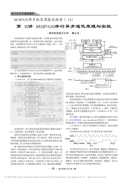
1.串口功能的实现(1)硬件串口 图1是MSP430系列芯片硬件串口的框图。
在该框图中,串口通讯由通讯速度的控制(数据位流的产生)、接收控制、发送控制等三部分构成。
波特率生成部分由时钟输入选择与分频、波特率发生器、调整器、波特率寄存器等组成。
串行通信时,接收与发送以什么样的速率将数据位收进或送出呢,这个速率就由波特率生成构件控制。
图2为其较为详细的结构。
整个模块的时钟源来自内部时钟或外部输入时钟,由SSEL1、SSEL0选择,以决定最终进入模块的时钟信号BRCLK的频率。
时钟信号BRCLK送入一个15位的分频器,通过一系列的硬件控制,最终输出移出与移进两移位寄存器使用的移位位时钟BITCLK信号。
那么这个信号(BITCLK)究竟是怎样产生的呢,从图的下半部分的一个波特率产生例子可以看出,是分频器在起作用。
当计数器减计数到“0”时,输出触发器翻转,送给BITCLK信号。
所以BITCLK信号周期的一半就是定时器(分频计数器)的定时时间。
接收控制部分与发送控制部分分别由两个移位寄存器构成。
接收时,当接收到一个完整数据,产生一个信号(URXIFG0=1),表示接收到完整数据,可以将此数据取走。
而在发送时,当一个数据正在发送过程中,UTXIFG0=1,此时,不能再发送数据,必须等当前数据发送完毕(UTXIFG0=0)时,方可继续发送。
串口接收一般采用中断方式,而发送数据则多采用主动方式。
在本刊的网站(www.eleworld.com)里给出了一段简单的完整通讯程序,实现的功能是将接收的数据原样送回。
(2)软件串口 而对于没有硬件串口的型号,如何实现异步串口功能呢?先分析异步串口的原理。
MSP430单片机与液晶显示器的串行接口方案设计(一)

MSP430单片机与液晶显示器的串行接口方案设计(一) 1概述点阵式液晶与外部的硬件接口简单,能以点阵或图形方式显示出各种信息,因此在电子设计中得到广泛应用。
但是,对它的接口设计必须遵循一定的硬件和时序规范,不同的液晶显示驱动器,可能需要采用不同的接口方式和控制指令才能够实现所需信息的显示。
某些液晶显示驱动器与外部的接口必须采用串行方式,而其串行接口往往不是标准的串行接口,这就为这类液晶显示驱动器的设计带来了困难。
针对上述问题,本文提出一种利用微控制器(MCU)的I/O端口,通过软件设计模拟与所使用的液晶显示驱动器规范相符的串行总线的设计思想,实现MCU对液晶显示驱动器的控制,从而建立起一套不但可以显示各种字符,而且可以动态显示曲线的游人显示系统。
2系统设计本文所建立的液晶显示系统,选用美国德州仪器(TI)公司的MSP430F149微控制器来控制液晶显示驱动器uPD16682A,从而实现各种信息的显示。
2.1MSP430F14X微控制器简介TI公司的MSP430F14X微控制器与其它MSP430系列微控制器相同,均甚至一个真正的正交16位RISCCPU内核:具有16个可单周期全寻址的16位寄存器,仅27条的精简指令集以及7种均采用双重取数据技术(DDFT)的一致性寻址方式。
DDFT技术利用每个时钟脉冲对存储器进行两次数据存取操作。
从而不再需要复杂的时钟乘法和指令流水线方案。
MSP430F14X系列MCU片内不但包括60多KB的Flash、2KB的RAM、一个看门狗时钟、12位16通道的A/D转换器、定时器、高精度比较器、PWM以及高速的USART控制器等常用资源,还在某些型号中集成了LCD控制器。
其I/O资源丰富,且每个输入/输出(I/O)引脚上都提供了矢量中断功能,每个外围器件都支持复杂的事件驱动型操作。
同其它微控制器相,带片内Flash的微控制器可将系统功耗降低5倍,并且减小了硬件线路板空间,与现代程序设计技术(如计算分支以及高级语言(如C语言)结合使用,使得MSP430的体系结构更为高效。
msp430多处理器之间的通信方式及协议
msp430多处理器之间的通信方式及协议
MSP430多处理器之间的通信方式主要有以下几种:
1.
串行通信:MSP430多处理器之间可以使用串行通信,如UART、I2C 、SPI等。
2.
并行通信:MSP430多处理器之间可以使用并行通信,如GPIO、DM A等。
3.
无线通信:MSP430多处理器之间可以使用无线通信,如ZigBee、Blu etooth等。
MSP430多处理器之间的通信协议主要有以下几种:
1. CAN:Controller Area
Network(控制器区域网络)是一种局域网技术,用于在汽车、工业控制和其他应用中连接多个设备。
2.
Modbus:Modbus是一种串行通信协议,用于在工业控制系统中连接多个设备。
3.
Ethernet:以太网是一种局域网技术,用于在局域网中连接多个设备。
4.
TCP/IP:TCP/IP是一种网络协议,用于在互联网上连接多个设备。
MSP430系列单片机模拟SPI串行口
MSP430系列单片机模拟SPI串行口1、SPI总线简述SPI(Serial Peripheral Interface串行外设接口)总线系统是一种同步串行外设接口,它可以使MCU与各种外围设备以串行方式进行通信以交换信息。
外围设置包括FLASHRAM、网络控制器、LCD显示驱动器、A/D转换器和MCU等。
SPI总线系统可直接与各个厂家生产的多种标准外围器件直接接口,该接口一般使用4条线:串行时钟线(SCK)、主机输入/从机输出数据线MISO、主机输出/从机输入数据线MOST和低电平有效的从机选择线SS(有的SPI接口芯片带有中断信号线INT或INT、有的SPI接口芯片没有主机输出/从机输入数据线MOSI)。
由于SPI系统总线一共只需3~4位数据线和控制即可实现与具有SPI总线接口功能的各种I/O器件进行接口,而扩展并行总线则需要8根数据线、8~16位地址线、2~3位控制线,因此,采用SPI总线接口可以简化电路设计,节省很多常规电路中的接口器件和I/O口线,提高设计的可靠性。
由此可见,在MCS51系列等不具有SPI接口的单片机组成的智能仪器和工业测控系统中,当传输速度要求不是太高时,使用SPI总线可以增加应用系统接口器件的种类,提高应用系统的性能。
2、MSP430系列单片机MSP430系列单片机是美国德州仪器(TI)1996年开始推向市场的一种16位超低功耗、具有精简指令集(RISC)的混合信号处理器。
称之为混合信号处理器,是由于其针对实际应用需求,将多个不同功能的模拟电路、数字电路模块和微处理器集成在一个芯片上,以提供“单片”解决方案。
MSP430系列单片机的IO口与51系列单片机的IO口不同,其单个引脚不能独立操作,必须对整个I/O口的寄存器进行置位(如无法对P1.0进行操作,只能对修改整个P1口的值)。
由此看来,对MSP430系列单片机IO口的操作要稍复杂于51系列单片机。
3、MSP430单片机模拟SPI串行口本文介绍一种用MSP430系列单片机的IO口模拟IIC接口的方法,模拟SCL和SDA两线接口的IIC接口类型。
MSP430同步串行通信SPI全解

选择SMCLK
配置波特率
UCB1IE |= UCRXIE; UCB1CTL1 &= ~UCSWRST
打开SPI中断 USCI_Bx复位释放
主机——其他配置
MST_Data = 0x01;
SLV_Data = 0x00;
主机初始化数据 从机初始化数据
#pragma vector=USCI_ B1_VECTOR __interrupt void USCI_ B1_ISR(void) { switch(__even_ase 2: while (!(UC B1IFG&UCTXIFG));
选择P8.4~P8.6端口方向为输出 选择P1.1~P1.0端口为输出 选择P1.1~P1.0端口为输出
主机——SPI模块初始化
UCB1CTL1 |= UCSWRST;
UCB1CTL0|=UCMST+UCSYNC+ UCCKPL+UCMSB; UCB1CTL1 |= UCSSEL_2; UCB1BR0 = 2; UCB1BR1 = 0;
串口中断缓冲器 UCBxRXBUF和UCBxTXBUF
UCRXBUFx: 接收缓冲器
UCTXBUFx: 发送缓冲器
应用示例
SPI主机与从机通过三线SPI接口通信,主机发送数据给从机,同时
又接收从机发来的数据,发送数据从0x01开始递增,从机接收到数据,
就立马发出,主机接到这个数据,进入中断如果发送和接收数据相同, 则点亮LED灯,否则熄灭。波特率为500kbps
程序流程图
主机 初始化SPI模块 初始化发送数据 MST_Data RX ISR
判断发送缓冲是否为空, 若是,则发送第一个字符 判断发送缓冲是否为空, 为空说明上次发送完毕
基于汇编语言的MSP430单片机与上位机间串行通讯的实现

I p e e to ra m m u c to t e M S 3 m lm n fSe ilCo nia i n bewe n P4 0 SCM nd a
Up r M a h ne Ba e n s m b y La ua e pe c i s d o As e l ng g
0 引言
的连 接 图 , 图 1所 示 , 用 到 了 MC 的 U A T 如 只 U S R 0模 块 和 L C 35的第二路转 换模块 , 中, R i T 18 其 T 2n脚与 MC U的 U X 0 T D 引脚连接 , X ot 与 MC R 2u脚 U的 U X 0引脚 连接。为了控 制和 R D
监 视 串 口通 讯 的工 作 情 况 , L C 35的脚 外 接 了一 个 开 关 和 在 T 18
随着电子技术 和集成 电路 制造工艺 的飞速发展 , 来越多 越
的控制 系统采用 了单 片机作为控 制核心 J 。在这些 系统 中 , 单 片机往往作为下位机使用 , C机常作 为上位 机使用 , 了使上 P 为
下 位 机 间能 实 现 对 话 , 要 建 立 上 下 位 机 间 的通 讯 联 系 。 由于 需
与 上 位 机 间 的硬 件 连 接 , 定 义 的 通 讯 协 议 的 基 础 上 , 用 汇 编 语 言 开 发 出 了单 片机 与 上 位 机 间 串行 通 讯 的程 序 。 调 试 在 采 实验 表 明硬 件 设 计 与软 件 开发 达到 了预 期 的 功 能 要 求 。 关键词 : P 3 MS 4 0单 片机 ; 串行 通 讯 ; 汇编 语 言 ; 讯 协 议 通 中 图分 类 号 :P 7 . T 23 5 文 献 标 识码 : B 文 章 编 号 :0 2—14 ( 00 0 07 0 10 8 1 2 1 )6— 0 5— 2
MSP430同步串行通信SPI解读

0: 不允许软件复位 1: 允许软件复位
UCB控制寄存器 UCBxCTL0
(USCI_Bx control register)
0: 从机模式 1: 主机模式 0: 8-bit data 1: 7-bit data
0: LSB first 1: MSB first 0: 时钟空闲状态为低电平 1: 时钟空闲状态为高电平 0: 前沿采样,后沿输出 1: 前沿输出,后沿采样
通用串行通信接口(USCI)模块
通用串行通信接口(USCI)模块支持多种串行通信模式。不 同的USCI 模块支持不同的模式 USCI_Ax 模块支持: UART 模式 IrDA 通信的脉冲整形 LIN 通信的自动波特率检测 SPI 模式 USCI_Bx 模块支持: I2C 模式 SPI 模式
MSP430模块特点
MSP430的SPI模块有如下特点: 支持3线或4线SPI操作 支持7位或8位数据格式 接收和发送有单独的移位寄存器 接收和发送有独立的缓冲器 接收和发送有独立的中断能力 时钟的极性和相位可编程 主模式的时钟频率可编程 传输速率可编程 支持连续收发操作 支持主从方式
UCBxIE
UCBxIFG UCBxIV
USCI_Bx中断使能
USCI_Bx中断标志 USCI_Bx中断向量
读 /写
读 /写 读
00h
02h 0000h
字节
字节 字
UCB控制寄存器 UCBxCTL1
(USCI_Bx control register)
00: 保留 01: ACLK 10:SMCLK 11:SMCLK
特点
优点: (1)接口简单,利于硬件设计与实现。 (2)时钟速度快,且没有系统开销。 (3)相对抗干扰能力强,传输稳定。
MSP430程序库(五)SPI同步串行通信
switch(dataBits)
{
case 7:case'7': UxCTL &=~ CHAR; break;
//7 位数据
case 8:case'8': UxCTL |= CHAR; break;
//8 位数据
default :
return(0);
//参数错误
}
//------------------------设置模式---------------------------
TxFlag=1; __low_power_mode_off_on_exit(); }
中断里面仅仅置标志位后,就退出低功耗;退出后即写入或者读取数据。
读取或写入函数调用的 SpiLpm 函数:
void SpiLpm()
{
if(UxTCTL&SSEL0) LPM3;
else
LPM0;
}
//若以 ACLK 作时钟,进入 LPM3 休眠(仅打开 ACLK) //若以 SMCLK 作时钟,进入 LPM0 休眠(不关闭 3; UTXIEx; // Enable USART0 RX interrupt
msp430串行异步通信
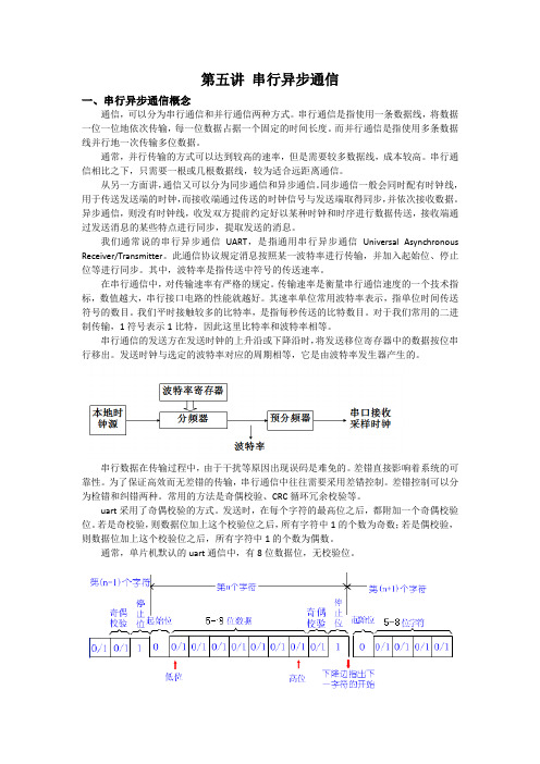
第五讲串行异步通信一、串行异步通信概念通信,可以分为串行通信和并行通信两种方式。
串行通信是指使用一条数据线,将数据一位一位地依次传输,每一位数据占据一个固定的时间长度。
而并行通信是指使用多条数据线并行地一次传输多位数据。
通常,并行传输的方式可以达到较高的速率,但是需要较多数据线,成本较高。
串行通信相比之下,只需要一根或几根数据线,较为适合远距离通信。
从另一方面讲,通信又可以分为同步通信和异步通信。
同步通信一般会同时配有时钟线,用于传送发送端的时钟,而接收端通过传送的时钟信号与发送端取得同步,并依次接收数据。
异步通信,则没有时钟线,收发双方提前约定好以某种时钟和时序进行数据传送,接收端通过发送消息的某些特点进行同步,提取发送的消息。
我们通常说的串行异步通信UART,是指通用串行异步通信Universal Asynchronous Receiver/Transmitter。
此通信协议规定消息按照某一波特率进行传输,并加入起始位、停止位等进行同步。
其中,波特率是指传送中符号的传送速率。
在串行通信中,对传输速率有严格的规定。
传输速率是衡量串行通信速度的一个技术指标,数值越大,串行接口电路的性能就越好。
其速率单位常用波特率表示,指单位时间传送符号的数目。
我们平时接触较多的比特率,是指每秒传送的比特数目。
对于我们常用的二进制传输,1符号表示1比特,因此这里比特率和波特率相等。
串行通信的发送方在发送时钟的上升沿或下降沿时,将发送移位寄存器中的数据按位串行移出。
发送时钟与选定的波特率对应的周期相等,它是由波特率发生器产生的。
串行数据在传输过程中,由于干扰等原因出现误码是难免的。
差错直接影响着系统的可靠性。
为了保证高效而无差错的传输,串行通信中往往需要采用差错控制。
差错控制可以分为检错和纠错两种。
常用的方法是奇偶校验、CRC循环冗余校验等。
uart采用了奇偶校验的方式。
发送时,在每个字符的最高位之后,都附加一个奇偶校验位。
六通道同步ADC与MSP430的接口设计
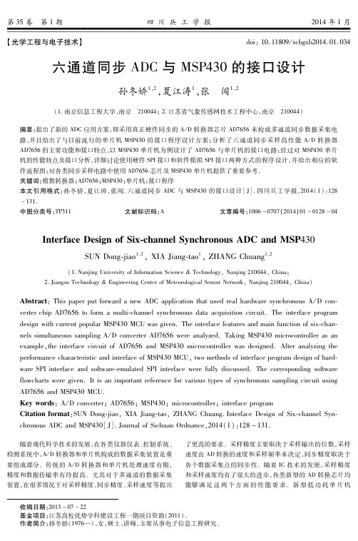
A b s t r a c t :T h i s p a p e r p u t f o r w a r dan e wA D Ca p p l i c a t i o nt h a t u s e dr e a l h a r d w a r es y n c h r o n o u s A/ Dc o n v e r t e r c h i pA D 7 6 5 6t of o r m am u l t i c h a n n e l s y n c h r o n o u sd a t aa c q u i s i t i o nc i r c u i t .T h ei n t e r f a c ep r o g r a m d e s i g nw i t hc u r r e n t p o p u l a r M S P 4 3 0M C Uw a s g i v e n .T h e i n t e r f a c e f e a t u r e s a n dm a i nf u n c t i o no f s i x c h a n n e l s s i m u l t a n e o u s s a m p l i n gA/ Dc o n v e r t e r A D 7 6 5 6w e r ea n a l y z e d .T a k i n gM S P 4 3 0m i c r o c o n t r o l l e r a s a n e x a m p l e , t h ei n t e r f a c ec i r c u i t o f A D 7 6 5 6a n dM S P 4 3 0m i c r o c o n t r o l l e r w a sd e s i g n e d .A f t e r a n a l y z i n gt h e , t w o m e t h o d s o f i n t e r f a c e p r o g r a md e s i g no f h a r d p e r f o r m a n c e c h a r a c t e r i s t i c a n di n t e r f a c e o f M S P 4 3 0M C U w a r eS P I i n t e r f a c ea n ds o f t w a r e e m u l a t e dS P I i n t e r f a c ew e r ef u l l yd i s c u s s e d .T h ec o r r e s p o n d i n gs o f t w a r e f l o w c h a r t s w e r eg i v e n .I t i s a ni m p o r t a n t r e f e r e n c ef o r v a r i o u s t y p e s o f s y n c h r o n o u s s a m p l i n gc i r c u i t u s i n g A D 7 6 5 6a n dM S P 4 3 0M C U . K e yw o r d s :A/ Dc o n v e r t e r ;A D 7 6 5 6 ;M S P 4 3 0 ;m i c r o c o n t r o l l e r ;i n t e r f a c ep r o g r a m C i t a t i o nf o r ma t : S U ND o n g j i a o ,X I AJ i a n g t a o ,Z H A N GC h u a n g . I n t e r f a c eD e s i g no f S i x c h a n n e l S y n c h r o n o u s A D Ca n dM S P 4 3 0 [ J ] . J o u r n a l o f S i c h u a nO r d n a n c e , 2 0 1 4 ( 1 ) : 1 2 8- 1 3 1 .
基于汇编语言的MSP430单片机与上位机间串行通讯的实现
2010年 第6期仪表技术与传感器Instrum ent T echn i que and Sensor 2010 N o 6基金项目:贵州省优秀科技教育人才省长资金资助项目(黔省专合字(2009)97号);贵州省高层次人才特助经费资助项目(TZJ F -2009年-24号)收稿日期:2009-09-23;收修改稿日期:2010-03-05基于汇编语言的M SP430单片机与上位机间串行通讯的实现吴怀超1,周 勇2,赵丽梅1(1.贵州大学机械工程学院,贵州贵阳 550003;2.杭州智源科技有限公司,浙江杭州 310030)摘要:对M SP430单片机与上位机间串行通讯的硬软件进行了开发,其中,通过电平转换芯片LTC1385实现了单片机与上位机间的硬件连接,在定义的通讯协议的基础上,采用汇编语言开发出了单片机与上位机间串行通讯的程序。
调试实验表明硬件设计与软件开发达到了预期的功能要求。
关键词:M SP430单片机;串行通讯;汇编语言;通讯协议中图分类号:TP273.5 文献标识码:B 文章编号:1002-1841(2010)06-0075-02I mp l e m ent of Serial Co mmunication betweenM SP430S C M andUpper M achine Based on A sse mbly L anguageWU H uai chao 1,Z HOU Y ong 2,ZHAO L i me i 1(1.School of M echan i cal E ngi n eer i ng ,G u izhou Un i versity ,G u i yang 550003,Ch i na ;2.H angzhou Z h i yuan T echnology Co .L td .,H angzhou 310030,Ch i na)Abstract :H ard w are and soft w are o f serial co mmunicati on bet w een M SP430SC M and upper machine w ere developed ,i nw hich ,the hardwa re connection bet w een SC M and uppe rm achi ne w as i m ple m ented t h rough e lectr i ca l leve l transfer chip LTC1385.A nd on the basis o f the defi n iti on of communicati on protoco ,l prog rams of ser i a l comm un i cation bet ween SC M and upper m achi ne w ere deve l oped us i ng assemb l y language .D ebugg i ng experi m ents i ndicate that ha rd w are desi gn and soft w are deve l op m ent hav e a t ta i ned the preplanned function requ ire m ents .K ey word s :M SP430SC M;se rial co mmunicati on ;sssemb l y language ;comm un i cation pro toco l 0 引言随着电子技术和集成电路制造工艺的飞速发展,越来越多的控制系统采用了单片机作为控制核心[1]。
MSP430教程15:MSP430单片机串行通讯模块
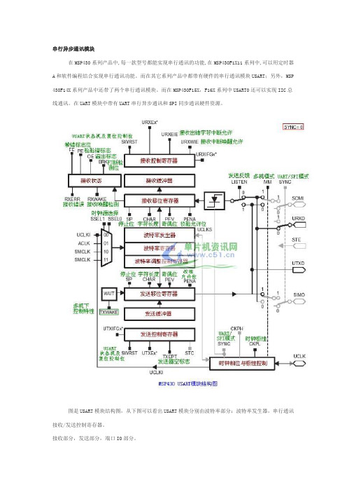
串行异步通讯模块在MSP430系列产品中,每一款型号都能实现串行通讯的功能,在MSP430F1X11系列中,可以用定时器A和软件编程结合实现串行通讯功能。
而在其它系列产品中都带有硬件的串行通讯模块USART;另外,MSP430F 14X系列产品中还带了两个串行通讯模块。
而在MSP430F15X,F16X系列中USART0还可以实现IIC总线通讯。
在UART模块中带有UART串行异步通讯和SPI同步通讯硬件资源。
图是USART模块结构图,从下图可以看出USART模块分别由波特率部分:波特率发生器,串行通讯接收/发送控制寄存器。
接收部分,发送部分,端口IO部分。
串行异步通讯的特点:1-异步通讯模式,包括线路空闲/地址位通信协议。
2-有两个单独的移位寄存器,输入/输出移位寄存器(如下图)。
3-传输7位或8位数据,可采用奇偶或无校验。
4-可编程实现波特率调整。
5-分别发,收单独中断。
6-有效地检测到起始位实现从低功耗唤醒。
7-状态标志检测错误或者地址位。
串行同步通讯(SPI)的特点:1-动持3线/4线的SPI通讯。
2-支持主机模式与从机模式。
3-收发有单独的缓冲器,移位寄存器。
4-收发有单独的中断。
5-时钟极性和相位可编程。
6-主机模式的时钟频率可编程。
7-7位/8位字符长度。
有关USART的详细应有原理,建议初学者参考清华大学出版社的<<MSP430系列16位超低功耗单片机原理与应用>>。
串行异步通讯应用例程//*******************************************//MSP430F149串口行实验程序//P3.4为发送,P3.5为接收//晶体使32768HZ.//程序描述:利用串口调试软件;向串口发送一个字符,MSP430单片机接收到后从低功耗中唤醒.并将收接缓冲区的字符再发送到//电脑上的调试软件中.单片机发送完后又进入低功耗状态.//*******************************************#include <msp430x14x.h>void main(void){WDTCTL = WDTPW + WDTHOLD; // 停止WDTUCTL0 = CHAR; // 设串口控制寄存器,设为8位字符格式UTCTL0 = SSEL0; // 设串口控制寄存器所使用的时钟,选择UCLK = ACLKUBR00 = 0x0D; // 波特率设置32k/2400 - 13.65UBR10 = 0x00;UMCTL0 = 0x6D; // 波特率调整器设置ME1 |= UTXE0 + URXE0; // 模块允许寄存器设置,使能USART0 TXD/RXDIE1 |= URXIE0; // 中断允许寄存器设置,接收中断允许P3SEL |= 0x30; // 将P3.4,5使用外围模块 = USART0 TXD/RXDP3DIR |= 0x10; // 将P3.4设为输出(发),P3.5默认为输入(收)_EINT(); // 全局中断使能// Mainloopfor (;;){LPM3; // 进入LPM3模式,等待字符接收.while ((IFG1 & UTXIFG0) == 0); // USART0发送UTXIFG0=1,表示UTXBUF准备好发送一下字符TXBUF0 = RXBUF0; // 将收到缓冲区字符送发送区}}//串口接收中断,退出LPM3模式.#pragma vector=USART0RX_VECTOR__interrupt void usart0_rx (void){LPM3_EXIT;}//*****************************************//例程结束。
- 1、下载文档前请自行甄别文档内容的完整性,平台不提供额外的编辑、内容补充、找答案等附加服务。
- 2、"仅部分预览"的文档,不可在线预览部分如存在完整性等问题,可反馈申请退款(可完整预览的文档不适用该条件!)。
- 3、如文档侵犯您的权益,请联系客服反馈,我们会尽快为您处理(人工客服工作时间:9:00-18:30)。
1ADS125X Data Converter Family 1.1ADS1251/52ADC Application ReportSLAA242–May2005INTERFACING THE ADS1251/52TO THE MSP430F449 Joe Purvis Data Acquisition Digital Analog ConvertersABSTRACTThis application report demonstrates an effective method to interface the ADS1251andADS1252sigma-delta data converters to the MSP430F449microcontroller.Thesoftware for this application report was developed on the HPA449development system.The ADS1251and the ADS1252are part of the ADS125x family of data converters.Table1lists the key features of each device in the family.For clarity,the features within the table are simplified.Consult the appropriate data sheet for specific device information.Table1.ADS125x Family FeaturesPOWERNUMBERRESOLUTION SPEED REGISTER NOMINALPART NUMBER OF CONSUMPTION(BITS)(KSPS)PROGRAMMABLE SUPPLYINPUTS(mW)VOLTAGE(S)VAnalog+5ADS12501Differential2025No75Digital+5ADS12511Differential2420No Analog+57.5ADS12521Differential2441No Analog+540ADS12534Differential2420No Analog+57.5ADS12544Differential2420No Analog+5 4.3Analog+5ADS12551Differential2430Yes36Digital+3.34Differential24Analog+5ADS125630Yes368Single24Digital+3.3endedThe ADS1251and ADS1252are24-bit,analog-to-digital converters;both incorporate the followingfunctions on-chip:•Fourth-order sigma-delta modulator•Digital filterThe block diagram in Figure1illustrates these functions.V REF CLKSCLK DOUT/DRDY +V DD GND+V IN −V IN1.2SIGMA-DELTAMODULATORADS125X Data Converter FamilyFigure 1.ADS1251/52Functional Block DiagramEach of these functions and the HPA449development system are discussed in the following sections.Figure 2.First-Order Sigma-Delta ModulatorThe foundation of the ADS1251/52is the sigma-delta modulator.Although detailed theory of this class of data converter is beyond the scope of this application report,the fundamental operation of this converter is discussed.Figure 2shows a first-order sigma-delta modulator,which operates as follows.The modulator’s function is to reduce the error between the input signal and the previous output to zero.Assuming a dc input at A,this dc value is applied to a summing point and added to the value from the DAC,E.If the output from the summing junction is positive,the integrator output continues to ramp up until it trips the comparator.The comparator then signals to the DAC that the input has passed its upper threshold.In turn,the DAC then begins to reduce the effective signal at B,and the integrator begins to ramp down.The integrator continues to ramp down until it trips the comparator again.The comparator then signals to the DAC that the input has passed its lower threshold.In turn,the DAC then begins to increase the effective signal at B,and the integrator begins to ramp up again.Because the comparator is latched,this action performs the quantization in time of the analog signal.The quantization in amplitude is accomplished through the density of the pulses originating from thecomparator.If the input signal is close to full scale,more 1pulses occur than 0pulses in the bit stream from the comparator.Conversely,if the input-signal is close to negative full scale,more 0pulses occur than 1pulses in the bit stream from the comparator.Signals near midscale have equal numbers of 1and 0pulses.Figure 3shows this graphically.1111111Integrator OutputComparator OutputIntegrator OutputComparator OutputV D = 0 VV D = V REF21.3DIGITAL FILTERADS125X Data Converter FamilyFigure parator Pulse Density1.2.1FOURTH-ORDER DELTA-SIGMA MODULATORThe modulator on an ADS125x converter is a fourth-order modulator constructed by cascading two single-bit,second-order modulators in a cascade or mesh topology.The two-modulator bit streams are then merged in a specific way to cancel out some of the unwanted lower order noise before they enter the digital filter.The process of averaging a time-domain signal is equivalent to performing a low-pass filtering operation.The more averages taken,the better characteristics the filter possesses,although the frequency response from an averager will always have a sinc characteristic.The digital filter incorporated in the ADS1251/52is referred to as a sinc 5filter.The sinc 2filter obtains the present value by averaging the previous two values.The sinc 3filter uses the previous three values toobtain the present value;similarly,the sinc 5filter uses the previous five values to obtain the present value.This is why,according to the ADS1251and ADS1252data sheets,the first valid data from the device does not occur until the sixth DOUT/DRDY cycle.Following this first valid cycle,every cycle thereafter contains valid data,although the data is the average of the previous five values.The digital filter attenuates the out-of-band noise and decimates the data by a factor of 64.The modulator clock for the EVM was set at 32.768kHz,although this can be easily altered to any valid modulator frequency.In this specific instance,the pass-band response is as shown in Figure 4.−400−300−200−10000.050.1G a i n − d Bf i − Input Frequency − kHz1.4HPA449DEVELOPMENT SYSTEMADS125X Data Converter FamilyFigure 4.ADS1252Pass-Band ResponseThe modulator clock establishes the data rate and the point of the notch in the frequency response.The sinc 5filter accomplishes a low-pass response with a high rejection of frequencies around 86Hz.The-3-dB point,in this case,is established around 20Hz;this is acceptable for precise low-frequency signals.In another example,if 50Hz is required to be rejected,the user can set the modulator clock to 19.2KHz.This yields a -3-dB point around 10Hz.The HPA449is the development system used to create the code that supports this application.Key features of this system follow.•MSP430F449processor •Custom LCD •RS-232Interface•JTAG programming headeris available directly from SoftBaugh,Inc.;consult the SoftBaugh Web site at2MSP430F449MicrocontrollerRST/NMIMSP430F449MicrocontrollerFigure 5is the functional block diagram for the MSP430F449.The peripheral modules of this microcontroller that are used in this application are shown in Figure 5.Figure 5.MSP430F449Functional Block DiagramTable 2.MSP430F449ModulesMODULE FUNCTION SUPPORTEDBIT FIELDCOMMENTSource MCLK Bit 1Diagnostic service,these bits may be I/O Port 1removed in software.Source ACLKBit 5I/O Port 2Interrupt from the ADC Bit 2Serial A on HPA449Bit 1SIMO (Data out)I/O Port 3USARTBit 2SOMI (Data in)Bit 3UCLK(SCLK)The timer supports two functions:Reset time –To ensure the ADC and MSP430aresynchronized,the ADC is reset.This is a period of at least 1536Timer_A3MCLKs.Wait time -Following an interrupt,data is not available until at least 36MCLKs have elapsed.3ADS1251/52DIGITAL INTERFACE BASICSMSP430F449ADS1251/523.1ADS1251/52OPERATING PROCEDUREDRDY Mode DOUT ModeDOUT ModeDRDY ModeDOUT/DRDYADS1251/52DIGITAL INTERFACE BASICSFigure 6shows the fundamental setup diagram.Figure 6.Interfacing the ADS1251/52to the MSP430DiagramThe ADS1251and ADS1252provide converted data as a serial bit stream to reduce the pin count and device size.The devices cannot be written to,only read from;this also reduces the complexity of the control required by the user.The digital interface can control the following five functions:•Power down the converter in a controlled manner •Power up the converter in a controlled manner •Synchronize the host system to the converter •Indicate when new data is available•Provide new data in a predictable mannerThe ADS1251and ADS1252accomplish these functions through two pins:•DOUT/DRDY -this is a multiplexed output pin that indicates when data is available to be read and also provides data to the host.•SCLK –the logic level and duration of SCLK controls the power state of the converter and alsoenables synchronization of the converter to a host system.In addition,SCLK is used to shift data from the device to the host system.To successfully use this class of ADC,users must recognize that the host has to complete a transfer during the time allotted to it by virtue of the modulator clock.In this specific case :Conversion cycle is 384*MCLK.This is 384*30.5µs =11.7ms,for this particular clock used.Each conversion cycle has two phases:a DRDY mode and a DOUT mode (see Figure 7).The DRDY mode consumes 36MCLK cycles,leaving the remaining 348MCLK cycles for data,DOUT mode.Therefore,it is clear that with a 32.768-kHz modulator clock,the three bytes of data must be read out within the allotted 348MCLK time,equivalent to 10.6ms.Figure 7.DOUT/DRDY PartioningADS1251/52DIGITAL INTERFACE BASICS To achieve successful conversions,several events must occur sequentially:•The system must be initialized.•The ADC must be synchronized.•Because only one pin is available for data and the signal indicating that data is(or is not)valid,the microprocessor must track whether the DOUT/DRDY pin is acting as either DOUT or DRDY.3.1.1INITIALIZATIONCertain steps are required for the initialization of the MSP430and the ADC.For the MSP430,the following peripheral modules must be initialized:•Clock source•Port2-Interrupt•Port3-USARTFor the ADS1251/52,these actions must be taken:•Reset the modulator of the ADC.•Prepare the ADC for a data transfer.The following discussion examines each of these steps in more detail. ADS1251/52DIGITAL INTERFACE BASICS3.1.1.1INITIALIZING THE CLOCK SOURCEvoid setup_osc(void)The clock modules and the control system for the MSP430F449are shown in Figure8.Figure8.MSP430F449Clock Modules and Control SystemTwo clocks are used in this application:•LFXT1•XT2LFXT1is a low-frequency crystal oscillator,sourced from the HPA449assembly.LFXT1has a frequency of32.768kHz.Reliable crystal operation depends on the proper load capacitance.This capacitance can be selected by software using the XCAPxPF bits.If the program fails to proceed past the Oscillator Flag check(LFOF),it may be necessary to change the XCAPxPF values in the program to ensure reliablefunction.The LFXT1clock is used to provide the clock for timer A.XT2can be used as the source of MCLK and SMCLK as shown in Figure8.In this application,XT2is derived from an8-MHz resonator connected between XT2IN and XT2OUT,and sourced by the user.(The resonator manufacturer used in this application is Murata,and the part number is CSTLS8M00G53-B0.) This resonator supplies the clocks required for the system,namely:•MCLK–Master Clock used by the system.•SMCLK–Sub-Main Clock,this clock is software selectable for individual peripheral modules.ADS1251/52DIGITAL INTERFACE BASICS SMCLK is the source clock for the USART(universal synchronous asynchronous receiver transmitter).The HPA449board has a location available(marked as X2on the silkscreen)where you can either solder the resonator directly to the HPA449or use a single-in-line socket strip,in case it becomes necessary to change resonators.It is useful to observe clock signals actually originating from the MSP430;this gives some assurance that the clocks required to operate the device are working as expected.On the MSP430F449,MCLK,SMCLK, and ACLK can be observed from select pins on the device,P1.1,P1.4,and P1.5,respectively.This can be achieved by setting P1.1,P1.4,and P1.5as special function and then setting each bit as an output.This enables MCLK,SMCLK,and ACLK to be monitored from P1.1,P1.4,and P1.5,respectively.Choose suitable points on the HPA449development board to probe the output signals.3.1.1.2INITIALIZING THE MSP430PORTSvoid setup_ports(void);This procedure sets the direction of the I/O ports.Inspection of the HPA449schematic indicates that the following bits should be set as inputs:BIT2—Interrupt AThis is the interrupt from serial site A,the serial site for which the program has been coded.BIT7—Interrupt BThis is the interrupt from serial site B,the other serial site.Because it may be used for futuresystems,also set this pin as an input.INTB is pulled HIGH through a47-kΩresistor,and becausethe system only responds to transitions,this causes no problems.3.1.1.3INITIALIZING THE MSP INTERRUPTSvoid setup_ints(void)Each pin on port2has interrupt capability.Any interrupt on P2sources a single interrupt vector for port2.Port2,bit2of the MSP430is set to receive an interrupt from the ADC;this interrupt is set to occur on a low-to-high transition.3.1.1.4USING TIMER AAn outline of the timer-A module and its control structure is shown in Figure9.The timer is used in two situations:•To determine enough time has elapsed for a valid reset of the modulator•To determine sufficient time has elapsed for DRDY mode to expire before reading data out of the device ADS1251/52DIGITAL INTERFACE BASICSFigure9.Timer-A Module Control StructureTimer A is set to use ACLK as its clock source.3.1.1.5RESETTING THE ADC MODULATORvoid reset_adc(float MCLK_PRD,float ACLK_PRD);With a running modulator clock and appropriate power applied to the converter,the DOUT/DRDY pincontinuously toggles between DOUT mode and DRDY mode.Therefore,it may be difficult for the host system to recognize an interrupt as an interrupt rather than recognize data as an interrupt.This problem is solved by asserting the signal to the SCLK pin HIGH.When this signal is asserted for a sufficient time,the modulator enters a reset state.The modulator can then be released from the resetstate in a controlled manner,by de-asserting the SCLK signal LOW.It is the action of de-asserting the SCLK signal that releases the modulator from reset and begins the DOUT/DRDY cycle.Resetting the ADS1251/52requires that the following condition be met:4*t DRDY<[SCLK=1]<20*t DRDYThis condition indicates that the SCLK signal should be asserted HIGH for at least four consecutiveDOUT/DRDY periods,but no more than20DOUT/DRDY periods,because more than20periods causes the modulator to power down.The DOUT/DRDY period is directly related to the modulator clock frequency as:SCLKDOUT/DRDYFor This Amount of Time The Host System Must Maintain SCLK HIGH.Note: D is 47.4 msADS1251/52DIGITAL INTERFACE BASICSt DRDY (Conversion cycle)=384*modulator clock periods.A modulator clock of 32.768kHz,as in this example,represents a clock period of 30.5µs,and a t DRDY time of 11.7ms.Therefore,to ensure that the modulator is reset,SCLK must be asserted HIGH for at least 4*t DRDY cycles;this is 4*11.7ms which is 46.8ms.This high-time reset is achieved by using the MSP430’s timer-A module (see Figure 9)and determining a count of clocks based on the ACLK period.This time period changes if either the modulator clock for the ADS1251/52is changed or the ACLK clock frequency is changed.Therefore,the calculation is achieved by passing two variables into the reset procedure:•MCLK_PRD •ACLK_PRDThe procedure determines the number of counts required based on timer A’s clock source and the period of the clock supplied to the ADS1251/52modulator.The program tests the interrupt flag,CCIFG,until the count has reached the value loaded into TACCR.Figure 10shows the reset cycle in this case.Figure 10.Reset CycleINTERFACING THE ADS1251/52TO THE MSP430F449SLAA242–May 200511*Refer to the device-specific data sheet for locationsADS1251/52DIGITAL INTERFACE BASICS3.1.1.6INITIALIZING THE USARTvoid setup_SPI(void)Figure 11shows the block diagram for the USART.Figure ART Block DiagramIn this application,the procedure is as follows:•Reset the USART module.•Enable SPI mode.•Set the specific SPI function bits (see Table 3).Table ART BIT ASSIGNMENTS (1)BIT POSITIONFUNCTION Bit 1SIMO (Data Out)Bit 2SOMI (Data In)Bit 3(2)UCLK (SCLK)(1)Table 3shows the bit assignment for the special function in the port 3module.(2)As soon as bit 3is assigned to the UCLK,the signal changes from a GPIO pin to the UCLK function.This asserts UCLK (SCLK for the ADS1251/52)LOW and causes the modulator of the ADC to be released from its reset state;consequently,the ADC’s continuous DOUT/DRDY cycle begins.INTERFACING THE ADS1251/52TO THE MSP430F44912SLAA242–May 20053.2RETRIEVING DATA ADS1251/52DIGITAL INTERFACE BASICS•Select SPI mode for the USART,in this case,master mode with sync=1and a character length of8 bits.•Select baud rate for the SPI clock,UCLK.•Select transmission protocol.•Release the USART module from reset mode.void make_array(void);This function reads512words of data and stores them in an array called ad_buffer.Following the LSB of data,the remaining time of DOUT mode is characterized by DOUT asserted LOW.The first rising edge after this time is the beginning of DRDY mode.The process generally proceeds as follows:•Wait until an interrupt occurs.•After an interrupt occurs,go to the interrupt service routine(ISR).•Wait for at least36MCLK periods,to ensure that the DRDY mode has concluded.•Read first byte of data(most significant byte)and shift left8bits.•Read second byte of data and shift left8bits.•Read third byte of data(least significant byte)and shift left8bits.•Increment the array index.•Return and wait for the next interrupt.A few additional comments are worthy of note regarding the ADC’s operation within the program’sboundary.After the interrupt occurs,an aggregate delay time denoted in the ADS1251and ADS1252data sheets as t4+t2+t3occurs before the end of the DRDY mode and the beginning of the DOUT mode.This time is (24+6+6)MCLK periods;in this example,the time therefore is36*30.5µs=1.1ms.Therefore,wait at least1.1ms before attempting to read any data from the device;this delay is realized by timer A indicating that the CCIFG flag is set.Figure12is a composite diagram showing the three sections of the DRDY phase:•24MCLKs HIGH•6MCLKs LOW•6MCLKs HIGHINTERFACING THE ADS1251/52TO THE MSP430F449SLAA242–May200513The interrupt to the MSP430occurs here.This is DRDY time − 36 MCLKsThe completion of the DRDY phase is here,36 MCLKs laterBegin clocking data into the MSP430 here.MCLKSCLKDOUT/DRDYSCLKDOUT/DRDYADS1251/52DIGITAL INTERFACE BASICSFigure 12.Three Sections of the DRDY PhaseBecause each data word from the ADC is 24bits long,and the SPI port of the MSP430is only 8bits wide,three bytes are required for one complete read.Each data word is constructed by waiting until the receive register indicates it is full (URXIFG0=1),reading the SPI receive register (U0RXBUF),storing the byte as appropriate,and repeating the procedure three times,to construct a 24-bit word.One complete 24-bit transfer is shown in Figure 13.Figure plete 24-Bit TransferThe result of the conversion is transmitted MSB first in an offset 2s-complement format.INTERFACING THE ADS1251/52TO THE MSP430F44914SLAA242–May 20054REFERENCESREFERENCESIn this example,both inputs to the ADC are at 0V;therefore,the code resolved by the ADC is close to 0x000000.The transfer function for the ADC is shown in Figure 14.Figure 14.ADC Transfer Function1.MSP430x4xx Family User’s Guide (SLAU056)2.MSP430x43x,MSP430x44x Mixed Signal Microcontroller (SLAS344)3.ADS1251,24-Bit,20kHz Analog-to-Digital Converter (SBAS184).4.ADS1252,24-Bit,40kHz Analog-to-Digital Converter (SBAS127)5.A Spreadsheet Calculating the Frequency Response of the ADS1250–54(SBAA103)6.Delta-Sigma Data Converters,Theory Design and Simulation ,R.Norsworthy,R.Schreier,and G.C.Temes,Wiley–IEEE Press,ISBN 0-7803-1045-4INTERFACING THE ADS1251/52TO THE MSP430F449SLAA242–May 200515IMPORTANT NOTICETexas Instruments Incorporated and its subsidiaries (TI) reserve the right to make corrections, modifications, enhancements, improvements, and other changes to its products and services at any time and to discontinue any product or service without notice. Customers should obtain the latest relevant information before placing orders and should verify that such information is current and complete. All products are sold subject to TI’s terms and conditions of sale supplied at the time of order acknowledgment.TI warrants performance of its hardware products to the specifications applicable at the time of sale in accordance with TI’s standard warranty. T esting and other quality control techniques are used to the extent TI deems necessary to support this warranty. Except where mandated by government requirements, testing of all parameters of each product is not necessarily performed.TI assumes no liability for applications assistance or customer product design. Customers are responsible for their products and applications using TI components. T o minimize the risks associated with customer products and applications, customers should provide adequate design and operating safeguards.TI does not warrant or represent that any license, either express or implied, is granted under any TI patent right, copyright, mask work right, or other TI intellectual property right relating to any combination, machine, or process in which TI products or services are used. Information published by TI regarding third-party products or services does not constitute a license from TI to use such products or services or a warranty or endorsement thereof. Use of such information may require a license from a third party under the patents or other intellectual property of the third party, or a license from TI under the patents or other intellectual property of TI.Reproduction of information in TI data books or data sheets is permissible only if reproduction is without alteration and is accompanied by all associated warranties, conditions, limitations, and notices. Reproduction of this information with alteration is an unfair and deceptive business practice. TI is not responsible or liable for such altered documentation.Resale of TI products or services with statements different from or beyond the parameters stated by TI for that product or service voids all express and any implied warranties for the associated TI product or service and is an unfair and deceptive business practice. TI is not responsible or liable for any such statements. Following are URLs where you can obtain information on other Texas Instruments products and application solutions:Products ApplicationsAmplifiers Audio /audioData Converters Automotive /automotiveDSP Broadband /broadbandInterface Digital Control /digitalcontrolLogic Military /militaryPower Mgmt Optical Networking /opticalnetwork Microcontrollers Security /securityTelephony /telephonyVideo & Imaging /videoWireless /wirelessMailing Address:Texas InstrumentsPost Office Box 655303 Dallas, Texas 75265Copyright 2005, Texas Instruments Incorporated。