4020EN103M2中文资料
(整理)o型耐油密封圈规格表分析

O型耐油密封圈材质:丁晴,硅胶,氟胶,及各种定制材料
O型耐油密封圈
O型耐油密封圈
O型耐油密封圈
O型耐油密封圈材质:丁晴,硅胶,氟胶,及各种定制材料
O型耐油密封圈
O型耐油密封圈材质:丁晴,硅胶,氟胶,及各种定制材料
O型耐油密封圈
古今名言
敏而好学,不耻下问——孔子
业精于勤,荒于嬉;行成于思,毁于随——韩愈
兴于《诗》,立于礼,成于乐——孔子
己所不欲,勿施于人——孔子
读书破万卷,下笔如有神——杜甫
读书有三到,谓心到,眼到,口到——朱熹
立身以立学为先,立学以读书为本——欧阳修
读万卷书,行万里路——刘彝
黑发不知勤学早,白首方悔读书迟——颜真卿
书卷多情似故人,晨昏忧乐每相亲——于谦
书犹药也,善读之可以医愚——刘向
莫等闲,白了少年头,空悲切——岳飞
发奋识遍天下字,立志读尽人间书——苏轼
鸟欲高飞先振翅,人求上进先读书——李苦禅
立志宜思真品格,读书须尽苦功夫——阮元
非淡泊无以明志,非宁静无以致远——诸葛亮
熟读唐诗三百首,不会作诗也会吟——孙洙《唐诗三百首序》书到用时方恨少,事非经过不知难——陆游
问渠那得清如许,为有源头活水来——朱熹
旧书不厌百回读,熟读精思子自知——苏轼
书痴者文必工,艺痴者技必良——蒲松龄
声明
访问者可将本资料提供的内容用于个人学习、研究或欣赏,以及其他非商业性或非盈利性用途,但同时应遵守著作权法及其他相关法律的规定,不得侵犯本文档及相关权利人的合法权利。
谢谢合作!。
PC4020 v3.0 中文说明书 图文

PC4020 v3.0 中文说明书图文PC4020 v3.0 ? 安装说明DLS-2 v1.3警告:本说明包括产品使用、功能和关于制造商责任方面的内容。
应仔细完整阅读本说明。
警告请仔细阅读安装者请注意此警告包括重要的资料。
作为与系统用户联系的唯一个体,您有责任使系统用户了解此警告的每个项目。
系统故障此系统经过认真设计,尽可能达到有效。
会出现某些情况,包括火警、盗警或其他不能提供保护的紧急情况。
任何类型的任何报警系统会考虑妥协,或由于种种原因而不能如期望般操作。
这些原因可能是:安装不当为了能够提供适当的保护,安防系统必须正确安装。
每次安装都必须由安防专业人员进行评估,以确保能覆盖所有访问点的区域。
门和窗上的锁和闩都必须是安全的,而且能正常操作。
窗、门、墙、天花板和其他建筑材料必须有足够的强度,而且建筑能够达到期望的保护水平。
在进行建筑活动期间或建筑活动后必须进行评估。
如果此设备可用的话,建议由消防队和/或警察局进行评估。
犯罪提示此系统的安防性能是十分可靠的。
有犯罪意向的人可能会从事降低这些安防性能有效性的研究。
定期检查安防系统是很重要的,可以确保性能保持有效,如果发现系统不能提供有效的保护,必须进行更新或替换。
侵入者的访问侵入者可以避开传感设备,从覆盖不足、断开连接警告设备的区域移动,或干涉及妨碍系统的正常运作,通过为被保护的访问点进入。
电源故障控制设备、入侵探测器、烟感探测器和许多其他的安防设备都需要适当的电源供应,便于正确操作。
如果设备用电池操作,电池可能出现故障。
即使电池不出故障,也必须充电、情况要良好以及安装正确。
如果只使用交流电,假设电流断开,哪怕只是暂时的,也会使设备在断电期间不能正常运作。
不同时间长度的电源中断往往伴随着会导致破坏电力设备如安防系统的电压波动。
发生电源中断后,要立即进行一次完整的系统测试,确保系统运作正常。
可替换电池的故障本系统的无线传送器经过特别设计,在一般情况下,电池寿命可达几年。
PMEM4020PD资料

2003 Nov 24
3
元器件交易网
Philips Semiconductors
Product specification
PNP transistor/Schottky-diode module
THERMAL CHARACTERISTICS SYMBOL Single device Rth(j-s) Rth(j-a) thermal resistance from junction to solder point thermal resistance from junction to ambient in free air; notes 1 and 2 in free air; notes 1 and 3 in free air; notes 1 and 4 in free air; notes 1 and 5 Combined device Rth(j-a) Notes thermal resistance from junction to ambient in free air; notes 1 and 3 PARAMETER CONDITIONS
2003 Nov 24
4
元器件交易网
Philips Semiconductors
Product specification
PNP transistor/Schottky-diode module
ELECTRICAL CHARACTERISTICS Tamb = 25 °C unless otherwise specified. SYMBOL PNP transistor ICBO ICEO IEBO hFE collector-base cut-off current collector-emitter cut-off current emitter-base cut-off current current gain (DC) VCB = −40 V; IE = 0 VCE = −30 V; IB = 0 VEB = −5 V; IC = 0 VCE = −5 V; IC = −1 mA VCE = −5 V; IC = −100 mA VCE = −5 V; IC = −500 mA VCE = −5 V; IC = −1 A VCE = −5 V; IC = −2 A; note 1 VCEsat collector-emitter saturation voltage IC = −100 mA; IB = −1 mA IC = −500 mA; IB = −50 mA IC = −1 A; IB = −100 mA IC = −2 A; IB = −200 mA VBEsat RCEsat VBEon fT base-emitter saturation voltage equivalent on-resistance base-emitter turn-on voltage transition frequency IC = −1 A; IB = −50 mA IC = −1 A; IB = −100 mA; note 1 VCE = −5 V; IC = −1 A IC = −50 mA; VCE = −10 V; f = 100 MHz − − − 300 300 250 160 50 − − − − − − − 150 PARAMETER CONDITIONS MIN.
Model 4020中文操作手册

4 操作本部分介绍如何设置和操作Model 4020分析仪。
4.1和4.5介绍准备步骤,从4.7开始介绍实际的操作。
4.2 事先断电检查在开始使用分析仪之前应断电检查,检查内容如下:1.看样气和载气的安装是否与安装和应用部分的要求一致(chapter 3)。
保证这些气体的安装在正确的位置,并且正确地接到分析仪的后部。
2.检查电路安装是否与安装部分(chapter 3)和输入输出表中的用法说明一致。
3.检查电路板和电缆/线的安装/连接是否正确。
4.确定记录器和报警器安装正确。
4.3 进入操作状态1.打开电源2.完成下述的空气调节之后,需要预热至少两个小时(加热传感器和取样系统)。
预热时间出厂时已经由软件设置好。
预热时,禁止点火。
4.4 气体调节4.4.1 空气1.调节空气瓶上的减压阀,将空气的压力调节到30psig。
2.调节仪器上的空气减压阀,将空气压力调节到指定的空气压力。
等空气流过传感器和预热完成之后,调节其他气体。
4.4.2 样气样气瓶压力调节到30psig(或者与样气压力匹配的压力),调节仪器上的样气调节阀,将样气压力调节到指定的样气压力。
4.4.3 标气1.将标气通入分析仪。
在样气和标气之间需要一个三通阀来实现二者间的切换。
2.将标气压力调节至30psig或者与样气压力匹配的压力。
3.调节仪器的样气压力,直到指定的样气压力,同时,旁路流量计读数为0.5到1.0SCFH。
4.4.4 燃烧气1.打开气瓶上的主阀门,将气瓶压力调节到30psig(或与样气压力匹配的压力)。
2.缓慢地打开气瓶上第二个阀门,以避免仪器上燃烧气减压阀受到过大的压力冲击。
注:LED红灯灭后,才能调节燃烧气。
4.5 点火当预热倒数计时器读数为零(传感器预热计时器)时,黄色加热器指示灯闪(表示温度控制其将温度保持在设置点上),红色点火失败指示灯亮。
预热完成后,4020会自动尝试点火,如果自动点火失败,一段时间后仪器会重新尝试点火,如果五次自动点火失败,就会显示一个点火失败信息。
JetWave 4020 4020E系列工业级802.11ac + 802.11n 2.4G WIF
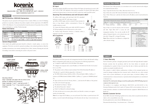
AppearanceJetWave 4020/4020E SeriesIndustrial 802.11ac + 802.11n 2.4G WIFI AP, 2xGT + USB M12Quick Installation Guide V1.0R&TTE Directive 1999/5/EC DeclarationThe product may be operated in all European Union countries. While you see the CE Marking printed on our product, it indicates the product complies with the requirement of the R&TTE (1995/5/EC) Directive. You can download the formal document of the product from our Web site or send inquiry to our Sales/Technical people.Only trained and qualified personnel should be allowed to install, replace, or service this equipment. The device can only be operated according to the technical specification. Read the installation instructions/user manual, including Power, Cable, Antenna, Warning info and well Grounding is must before connecting the system to the power source.DC InputThe device supports dual DC power input or Passive PoE input, the typical power source is DC 24V (±15%) or DC 110V depends on the model you purchase. For passive PoE input, please purchase the injector from us, the device do NOT accept force mode from PSE switch.The Korenix View Utility provides you convenient tool to scan the network and configure the connected Korenix device.Step 1: Open the Korenix View Utility. (Must later than V1.6.11)Step 2: Select the correct NIC (Network Interface Card) from the NIC list.Step 3: Click “Discovery”, and then the Nodes and its IP address can be found and listed in Node list.Step 4: After you scan the network, select the deviceand click “Open Web GUI” to access the web management interface. You can also modify the IP address/Netmask directly on the selected entry and then click “Change IP“ to change IP settings.Note: Please check the User Manual to configure theother software settings.3 Years WarrantyEach of Korenix’s product is designed, produced, and tested with high industrial standard. Korenix warrants that the product(s) shall be free from defects in materials and workmanship for a period of three (3) years from the date of delivery provided that the product was properly installed and used.This warranty is voided if defects, malfunctions or failures of the warranted product are caused by damage resulting from force measure (such as floods, fire, etc.), other external forces such as power disturbances, over spec power input, or incorrect cabling; or the warranted product is misused, abused, or operated, altered and repaired in an unauthorized or improper way.Attention! To avoid system damage caused by sparks, please DO NOT plug in power connector when power is on.The product is in compliance with Directive 2002/95/EC and 2011/65/EU of the European Parliament and of the Council of 27 January 2003 on the restriction of the use of certain hazardous substances in electrical and electronics equipment (RoHS Directives &RoHS 2.0)Korenix Customer ServiceKoreCARE is Korenix Technology's global service center, where our professional staffs are ready to solve your problems at any time.Korenixglobalservicecenter:********************.Document download: -> DownloadSupportThe JetWave 4020 Series provides web management interface for basic and advanced settings. Before configuration, please make sure your system meets the following requirements:A computer coupled with 10/100/1000 Base-T(X) adapter.Configure the computer with a static IP address of 192.168.10.X/192.168.1.X (X cannotbe 0, 1, nor 255).The product works as Router mode in default. The GT2(LAN) default IP address is“192.168.10.1”, and GT1 (WAN) default IP is “192.168.1.1”The WIFI default setting of JetWave 4020 is AP mode, Radio1 SSID is “JetWave_1”,operate in 2437MHz(channel 6).Radio2 SSID is “JetWave_2”, operate in 5180MHz(channel 36).Open web browser (Ex: IE, Chrome, Firefox…) and enter the IP address of the product.You will see the System Login page.The default User Name is “admin”.The default Password is “admin”.Check User Manual for advanced settings.If the web browser is not access, please check your firewall or contact your supportwindow for further help.Note: If you forget the IP Address, you can use Korenix View Utility to search the device’s IPaddress, it can be found at Download page of the Korenix web site: Web GUIRadio InformationEthernet 1 ----- 0P 2 ----- 0N 3 ----- 1P 4 ----- 1N5 ----- 3P6 ----- 3N7 ----- 2N8 ----- 2P23758461USB + Console1 ----- TX2 ----- RX3 ----- GND4 ----- GND5 ----- USB DP6 ----- USB DM7 ----- USB +5V8 ----- GND Power Input 2:+ 1:+ 3:- 4:-Upper panelLower panelWLAN 1(2.4G)WLAN 2(5G)JetWave 4020Embedded Ant.(2.4G 9dBi + 5G 10dBi)JetWave 4020E 4x N-Type Ant.GroundingRF CableLightening Protection ArrestorMounting method:Step2: Assemble Step3: Assemble mounting Case plateJetWave 4020 equips with dual band 2.4G+5G embeddedantenna, it can provide 180owide range coverage.JetWave 4020E equips with the external N-Type antennas forshort or long distance wireless communication. Choose the suitable antenna you need.Connect the Ethernet cable, power cable with M12 connector. Well grounding the device before power on the system.Connect Surge Protection Arrestor at Antenna socket isimportant to protect your system on field.M12 ConnectorMounting The Unit/Antenna and well Ground is MUSTR&TTE 指令1999/5/EC 宣告该产品可在所有欧盟国家进行操作。
ADM1032资料

REV.0Information furnished by Analog Devices is believed to be accurate and reliable. However, no responsibility is assumed by Analog Devices for its use, nor for any infringements of patents or other rights of third parties that may result from its use. No license is granted by implication or otherwise under any patent or patent rights of Analog Devices.aADM1032*One Technology Way, P.O. Box 9106, Norwood, MA 02062-9106, U.S.A.Tel: 781/ Fax: 781/326-8703© Analog Devices, Inc., 2001؎1؇C Remote and Local System Temperature MonitorFUNCTIONAL BLOCK DIAGRAMDDTHERMD+FEATURESOn-Chip and Remote Temperature Sensing Offset Registers for System Calibration0.125؇C Resolution/1؇C Accuracy on Remote Channel 1؇C Resolution/3؇C Accuracy on Local Channel Fast (Up to 64 Measurements per Second)2-Wire SMBus Serial Interface Supports SMBus AlertProgrammable Over/Under Temperature Limits Programmable Fault QueueOver-Temperature Fail-Safe THERM Output Programmable THERM LimitsProgrammable THERM Hysteresis 170 A Operating Current 5.5 A Standby Current 3 V to 5.5 V SupplySmall 8-Lead SO and Micro_SO Package APPLICATIONSDesktop Computers Notebook Computers Smart BatteriesIndustrial Controllers Telecomms Equipment Instrumentation Embedded SystemsPentium is a registered trademark of Intel Corporation.*Patents 5,982,221, 6,097,239, 6,133,753, 6,169,442, 5,867,012.PRODUCT DESCRIPTIONThe ADM1032 is a dual-channel digital thermometer and under/over temperature alarm, intended for use in personal computers and thermal management systems. The higher 1°C accuracy offered allows systems designers to safely reduce temperature guardbanding and increase system performance.The device can measure the temperature of a microprocessor using a diode-connected NPN or PNP transistor, which may be provided on-chip or can be a low-cost discrete device such as the 2N3906. A novel measurement technique cancels out the absolute value of the transistor’s base emitter voltage, so that no calibration is required. The second measurement channel mea-sures the output of an on-chip temperature sensor, to monitor the temperature of the device and its environment.The ADM1032 communicates over a two-wire serial interface compatible with System Management Bus (SMBus) standards.Under and over temperature limits can be programmed into the device over the serial bus, and an ALERT output signals when the on-chip or remote temperature measurement is out of range.This output can be used as an interrupt, or as an SMBus alert.The THERM output is a comparator output that allows CPU clock throttling or on/off control of a cooling fan.ADM1032–SPECIFICATIONS(T A = T MIN to T MAX, V DD = V MIN to V MAX, unless otherwise noted.)Parameter Min Typ Max Unit Test Conditions/CommentsPOWER SUPPLYSupply Voltage, V DD 3.0 3.30 5.5VAverage Operating Supply Current, I CC170215µA0.0625 Conversions/Sec Rate15.510µA Standby ModeUndervoltage Lockout Threshold 2.35 2.55 2.8V V DD Input, Disables ADC, Rising Edge Power-On Reset Threshold1 2.4VTEMPERATURE-TO-DIGITAL CONVERTERLocal Sensor Accuracy±1±3°C0 ≤ T A≤ 100°C, V CC = 3 V to 3.6 V Resolution1°CRemote Diode Sensor Accuracy±1°C60°C ≤ T D≤ 100°C, V CC = 3 V to 3.6 V±3°C0°C ≤ T D≤ 120°CResolution0.125°CRemote Sensor Source Current230µA High Level, Note 213µA Low Level, Note 2Conversion Time35.7142.8ms From Stop Bit to Conversion Complete(Both Channels) One-Shot Mode withAveraging Switched On5.722.8ms One-Shot Mode with Averaging Off(i.e., Conversion Rate = 32 or 64Conversions per Second)OPEN-DRAIN DIGITAL OUTPUTS(THERM, ALERT)Output Low Voltage, V OL0.4V I OUT = –6.0 mA2High Level Output Leakage Current, I OH0.11µA V OUT = V DD2SMBus INTERFACE2Logic Input High Voltage, V IH 2.1V V DD = 3 V to 5.5 VSCLK, SDATALogic Input Low Voltage, V IL0.8V V DD = 3 V to 5.5 VHysteresis500mVSCLK, SDATASMBus Output Low Sink Current6mA SDATA Forced to 0.6 VALERT Output Low Sink Current1mA ALERT Forced to 0.4 VLogic Input Current, I IH, I IL–1+1µASMBus Input Capacitance, SCLK, SDATA5pFSMBus Clock Frequency100kHzSMBus Timeout2564ms Note 3SMBus Clock Low Time, t LOW 4.7µs t LOW between 10% PointsSMBus Clock High Time, t HIGH4µs t HIGH between 90% PointsSMBus Start Condition Setup Time, t SU:STA 4.7µsSMBus Start Condition Hold Time, t HD:STA4µs Time from 10% of SDATA to 90%of SCLKSMBus Stop Condition Setup Time, t SU:STO4µs Time from 90% of SCLK to 10%of SDATASMBus Data Valid to SCLK Rising Edge250ns Time for 10% or 90% of SDATA to Time, t SU:DAT10% of SCLKSMBus Data Hold Time, t HD:DAT300µsSMBus Bus Free Time, t BUF 4.7µs Between Start/Stop ConditionSCLK Falling Edge to SDATA1µs Master Clocking in DataValid Time, t VD,DATSCLK, SDATA Rise Time, t R1µsSCLK, SDATA Fall Time, t F300nsNOTES1See Table VI for information on other conversion rates.2Guaranteed by Design, not production tested.3The SMBus timeout is a programmable feature. By default it is not enabled. Details on how to enable it are available in the SMBus section of this data sheet. Specifications subject to change without notice.–2–REV. 0REV. 0–3–ADM1032Figure 1.Diagram for Serial Bus TimingORDERING GUIDETemperature Package Package Branding SMBus Model Range DescriptionOption Information Addr ADM1032AR0°C to 120°C 8-Lead SO PackageSO-81032AR 4C ADM1032ARM0°C to 120°C8-Lead Micro_SO PackageRM-8T2A4CPIN CONFIGURATIONPIN FUNCTION DESCRIPTIONSPin No.Mnemonic Description1V DD Positive Supply, 3 V to 5.5 V.2D+Positive Connection to Remote Temperature Sensor.3D–Negative Connection to Remote Temperature Sensor.4THERM Open-drain output that can be used to turn a fan on/off or throttle a CPU clock in the event of an over-temperature condition. Requires pull-up to V DD .5GND Supply Ground Connection6ALERT Open-Drain Logic Output Used as Interrupt or SMBus Alert.7SDATA Logic Input/Output, SMBus Serial Data. Open-Drain Output. Requires pull-up resistor.8SCLKLogic Input, SMBus Serial Clock. Requires pull-up resistor.ABSOLUTE MAXIMUM RATINGS *Positive Supply Voltage (V DD ) to GND . . . . . . –0.3 V, +5.5 V D+ . . . . . . . . . . . . . . . . . . . . . . . . . . . . –0.3 V to V DD + 0.3 V D– to GND . . . . . . . . . . . . . . . . . . . . . . . . . –0.3 V to +0.6 V SCLK, SDATA, ALERT . . . . . . . . . . . . . . . . –0.3 V to +5.5 V THERM . . . . . . . . . . . . . . . . . . . . . . . –0.3 V to V DD + 0.3 V Input Current, SDATA, THERM . . . . . . . . . . . –1, +50 mA Input Current, D– . . . . . . . . . . . . . . . . . . . . . . . . . . . . ±1 mA ESD Rating, All Pins (Human Body Model) . . . . . . >1000 V Maximum Junction Temperature (T J max) . . . . . . . . . 150°C Storage Temperature Range . . . . . . . . . . . . –65°C to +150°C IR Reflow Peak Temp . . . . . . . . . . . . . . . . . . . . . . . . . 220°C Lead Temp (Soldering 10 sec) . . . . . . . . . . . . . . . . . . . 300°C*Stresses above those listed under Absolute Maximum Ratings may cause permanent damage to the device. This is a stress rating only; functional operation of the device at these or any other conditions above those indicated in the operational section of this specification is not implied. Exposure to absolute maximum rating conditions for extended periods may affect device reliability.THERMAL CHARACTERISTICS8-Lead SO Package θJA = 121°C/W8-Lead Micro_SO Package θJA = 142°C/WREV. 0ADM1032–Typical Performance Characteristics–4–LEAKAGE RESIST ANCE – M ⍀T E M P E R A T U R E E R R O R – ؇C101002016–160–4–8–128412TPC 1. Temperature Error vs.Leakage Resistance FREQUENCY – HzT E M P E R A T U R E E R R O R – ؇C101M24681012TPC 4.Temperature Error vs. Power Supply Noise FrequencyFREQUENCY – HzT E M P E R A T U R E E R R O R – ؇C024681012100k1M 10M 100MTPC 7.Temperature Error mon-Mode Noise Frequency T E M P E R A T U R E E R R O R – ؇C–0.50.51.0TEMPERA TURE – ؇C20406080100120TPC 2.Temperature Error vs. Actual Temperature Using 2N390616111621263118160T E M P E R A T U R E E R R O R – C864212101436CAP ACIT ANCE – nFTPC 5.Temperature Error vs.Capacitance between D+ and D–SCLK FREQUENCY – kHz1510255075100S U P P L Y C U R R E N T – A2505007501000TPC 8.Standby Supply Current vs.Clock Frequency FREQUENCY – Hz1311–1100k100M1MT E M P E R A T U R E E R R O R – C10M 75319TPC 3.Temperature Error vs.Differential Mode Noise FrequencyCONVERSION RA TE – Hz0.01S U P P L Y C U R R E N T – A0.1110100TPC 6.Operating Supply Current vs. Conversion RateSUPPL Y VOL T AGE – V400S T A N D B Y S U P P L Y C U R R E N T – A1.52.50.5 1.03.0 5.03.54.0 4.52.03530252015105TPC 9.Standby Supply Current vs.Supply VoltageREV. 0ADM1032–5–FUNCTIONAL DESCRIPTIONThe ADM1032 is a local and remote temperature sensor and over-temperature alarm. When the ADM1032 is operating normally, the on-board A-to-D converter operates in a free-running mode. The analog input multiplexer alternately selects either the on-chip temperature sensor to measure its local tem-perature, or the remote temperature sensor. These signals are digitized by the ADC and the results stored in the Local and Remote Temperature Value Registers.The measurement results are compared with local and remote,high, low and THERM temperature limits, stored in nine on-chip registers. Out-of-limit comparisons generate flags that are stored in the Status Register, and one or more out-of limit results will cause the ALERT output to pull low. Exceeding THERM temperature limits cause the THERM output to assert low.The limit registers can be programmed, and the device con-trolled and configured, via the serial System Management Bus (SMBus). The contents of any register can also be read back via the SMBus.Control and configuration functions consist of:•Switching the device between normal operation and standby mode.•Masking or enabling the ALERT output.•Selecting the conversion rate.MEASUREMENT METHODA simple method of measuring temperature is to exploit the negative temperature coefficient of a diode, or the base-emitter voltage of a transistor, operated at constant current. Unfortu-nately, this technique requires calibration to null out the effect of the absolute value of V BE , which varies from device to device.The technique used in the ADM1032 is to measure the change in V BE when the device is operated at two different currents.This is given by:where:K is Boltzmann’s constant (1.38 × 10⁻²³).q is charge on the electron (1.6 × 10⁻¹⁹ Coulombs).T is absolute temperature in Kelvins.N is ratio of the two currents.n f is the ideality factor of the thermal diode.The ADM1032 is trimmed for an ideality factor of 1.008.Figure 2 shows the input signal conditioning used to measure the output of an external temperature sensor. This figure shows the external sensor as a substrate transistor, provided for tem-perature monitoring on some microprocessors, but it could equally well be a discrete transistor. If a discrete transistor is used, the collector will not be grounded, and should be linked to the base. To prevent ground noise interfering with the measure-ment, the more negative terminal of the sensor is not referenced to ground, but is biased above ground by an internal diode at the D– input. If the sensor is operating in a noisy environment,C1 may optionally be added as a noise filter. Its value is typi-cally 2200 pF, but should be no more than 3000 pF. See the section on Layout Considerations for more information on C1.To measure ∆V BE , the sensor is switched between operating cur-rents of I and N × I. The resulting waveform is passed through a 65 kHz low-pass filter to remove noise, thence to a chopper-stabilized amplifier that performs the functions of amplification and rectification of the waveform to produce a dc voltage pro-portional to ∆V BE . This voltage is measured by the ADC to give a temperature output in two’s complement format. To further reduce the effects of noise, digital filtering is performed by aver-aging the results of 16 measurement cycles.Signal conditioning and measurement of the internal tempera-ture sensor is performed in a similar manner.TEMPERATURE DATA FORMATOne LSB of the ADC corresponds to 0.125°C, so the ADC canmeasure from 0°C to 127.875°C. The temperature data format is shown in Tables I and II.The results of the local and remote temperature measurements are stored in the Local and Remote Temperature Value Registers,and are compared with limits programmed into the Local and Remote High and Low Limit Registers.Table I.Temperature Data Format (Local Temperature and Remote Temperature High Byte)Temperature Digital Output 0°C 000000001°C 0000000110°C 0000101025°C 0001100150°C 0011001075°C 010********°C 01100100125°C 01111101127°C01111111REMOTE SENSING V OUT+TO ADC V OUT –C1 = 2.2nF TYPICAL, 3nF MAX.Figure 2.Input Signal Conditioning∆V n KT q In N BE f =()×()ADM1032–6–Status RegisterBit 7 of the Status Register indicates that the ADC is busy con-verting when it is high. Bits 6 to 3, 1, and 0 are flags that indicate the results of the limit comparisons. Bit 2 is set when the remote sensor is open circuit.If the local and/or remote temperature measurement is above the corresponding high temperature limit, or below or equal to, the corresponding low temperature limit, one or more of these flags will be set. These five flags (Bits 6 to 2) NOR’d together, so that if any of them is high, the ALERT interrupt latch will be set and the ALERT output will go low. Reading the Status Register will clear the five flag bits, provided the error conditions that caused the flags to be set have gone away. While a limit comparator is tripped due to a value register containing an out-of-limit measure-ment, or the sensor is open circuit, the corresponding flag bit cannot be reset. A flag bit can only be reset if the corresponding value register contains an in-limit measurement or the sensor is good. The ALERT interrupt latch is not reset by reading the Status Register, but will be reset when the ALERT output has been serviced by the master reading the device address, provided the error condition has gone away and the Status Register flag bits have been reset.When Flags 1 and 0 are set, the THERM output goes low to indicate that the temperature measurements are outside the programmed limits. THERM output does not need to be reset, unlike the ALERT output. Once the measurements are within the limits, the corresponding Status register bits are reset and the THERM output goes high.Table IV. Status Register Bit AssignmentsBit Name Function7BUSY 1 When ADC Converting6LHIGH* 1 When Local High-Temp Limit Tripped5LLOW* 1 When Local Low-Temp Limit Tripped4RHIGH* 1 When Remote High-Temp Limit Tripped3RLOW* 1 When Remote Low-Temp Limit Tripped2OPEN* 1 When Remote Sensor Open-Circuit1RTHRM 1 When Remote Therm Limit Tripped0LTHRM 1 When Local Therm Limit Tripped*These flags stay high until the status register is read or they are reset by POR. Configuration RegisterTwo bits of the Configuration Register are used. If Bit 6 is 0, which is the power-on default, the device is in operating mode with the ADC converting. If Bit 6 is set to 1, the device is in standby mode and the ADC does not convert. The SMBus does, however, remain active in Standby Mode so values can be read from or written to the SMBus. The ALERT and THERM O/Ps are also active in Standby Mode.Bit 7 of the configuration register is used to mask the alert output. If Bit 7 is 0, which is the power-on default, the output is enabled. If Bit 7 is set to 1, the output is disabled.Table II.Extended Temperature Resolution (RemoteTemperature Low Byte)Extended Remote TemperatureResolution Low Byte0.000°C000000000.125°C001000000.250°C010000000.375°C011000000.500°C100000000.625°C101000000.750°C110000000.875°C11100000ADM1032 REGISTERSThe ADM1032 contains registers that are used to store theresults of remote and local temperature measurements, high andlow temperature limits, and to configure and control the device.A description of these registers follows, and further details aregiven in Tables III to VII.Address Pointer RegisterThe Address Pointer Register itself does not have, or require, anaddress, as it is the register to which the first data byte of everyWrite operation is written automatically. This data byte is anaddress pointer that sets up one of the other registers for thesecond byte of the Write operation, or for a subsequent readoperation.The power-on default value of the Address Pointer Register is00h, so if a read operation is performed immediately after power-on without first writing to the Address Pointer, the value of thelocal temperature will be returned, since its register address is 00h.Value RegistersThe ADM1032 has three registers to store the results of Localand Remote temperature measurements. These registers arewritten to by the ADC only and can be read over the SMBus.Offset RegisterSeries resistance on the D+ and D– lines in processor packagesand clock noise can introduce offset errors into the remote tem-perature measurement. To achieve the specified accuracy onthis channel these offsets must be removed.The offset value is stored as an 11-bit, two’s complement valuein registers 11h (high byte) and 12h (low byte, left justified).The value of the offset is negative if the MSB of register 11h is 1and it is positive if the MSB of register 12h is 0. The value isadded to the measured value of remote temperature.The offset register powers up with a default value of 0°C, andwill have no effect if nothing is written to them.Table III.Sample Offset Register CodesOffset Value11h12h–4°C1111110000000000–1°C1111111100000000–0.125°C1111 1111111000000°C0000000000000000+0.125°C0000000000100000+1°C0000000100000000+4°C0000010000000000REV. 0REV. 0ADM1032–7–Consecutive ALERT RegisterThis value written to this register determines how many out-of-limit measurements must occur before an ALERT is generated.The default value is that one out-of-limit measurement gener-ates an ALERT . The max value that can be chosen is 4. The purpose of this register is to allow the user to perform some filter-ing of the output. This is particularly useful at the faster two conversion rates where no averaging takes place.Table VII.Number of “Out-of-Limit”Register Value Measurements Required yxxx 000x 1yxxx 001x 2yxxx 011x 3yxxx 111x4NOTESx = Don’t care bit.y = SMBus timeout bit. Default = 0. See SMBus section for more information.SERIAL BUS INTERFACEControl of the ADM1032 is carried out via the serial bus. The ADM1032 is connected to this bus as a slave device, under the control of a master device.There is a programmable SMBus timeout. When this is enabled the SMBus will timeout after typically 25 ms of no activity. How-ever, this feature is not enabled by default. To enable it, set Bit 7of the Consecutive Alert Register (Addr = 22h).The ADM1032 supports Packet Error Checking (PEC) and its use is optional. It is triggered by supplying the extra clock for the PEC byte. The PEC byte is calculated using CRC-8. The Frame Check Sequence (FCS) conforms to CRC-8 by the polynomial:C (x ) = x 8 + x 2 + x 1 + 1Consult SMBus 1.1 specification for more information ().ADDRESSING THE DEVICEIn general, every SMBus device has a 7-bit device address (except for some devices that have extended, 10-bit addresses). When the master device sends a device address over the bus, the slave device with that address will respond. The ADM1032 is avail-able with one device address, which is Hex 4C (1001 100).The serial bus protocol operates as follows:1.The master initiates data transfer by establishing a START condition, defined as a high-to-low transition on the serial data line SDATA, while the serial clock line SCLK remains high. This indicates that an address/data stream will follow.All slave peripherals connected to the serial bus respond to the START condition, and shift in the next eight bits, con-sisting of a 7-bit address (MSB first) plus an R/W bit, which determines the direction of the data transfer, i.e., whether data will be written to or read from the slave device.The peripheral whose address corresponds to the transmitted address responds by pulling the data line low during the low period before the ninth clock pulse, known as the Acknowl-edge Bit. All other devices on the bus now remain idle while the selected device waits for data to be read from or written Table V. Configuration Register Bit AssignmentsPower-On Bit Name FunctionDefault 7MASK10 = ALERT Enabled 01 = ALERT Masked 6RUN/STOP0 = Run 01 = Standby 5–0ReservedConversion Rate RegisterThe lowest four bits of this register are used to program the conversion rate by dividing the internal oscillator clock by 1, 2,4, 8, 16, 32, 64, 128, 256, 512, or 1024 to give conversion times from 15.5 ms (code 0Ah) to 16 seconds (code 00h). This register can be written to and read back over the SMBus. The higher four bits of this register are unused and must be set to zero. Use of slower conversion times greatly reduces the device power consumption, as shown in Table VI.Table VI.Conversion Rate Register CodesAverage Supply Current Data Conversion/sec mA Typ at V DD = 5.5 V 00h 0.06250.1701h 0.1250.2002h 0.250.2103h 0.50.2404h 10.2905h 20.4006h 40.6107h 8 1.108h 16 1.909h 320.730Ah641.230B to FFhReservedLimit RegistersThe ADM1032 has nine Limit Registers to store local and remote,high, low, and THERM temperature limits. These registers can be written to and read back over the SMBus.The high limit registers perform a > comparison while the low limit registers perform a < comparison. For example, if the high limit register is programmed with 80°C, then measuring 81o C will result in an alarm condition. If the Low Limit Register is programmed with 0°C, measuring 0°C or lower will result in Alarm condition. Exceeding either the Local or Remote THERM limit asserts THERM low. A default hysteresis value of 10°C is provided, which applies to both channels. This hysteresis may be reprogrammed to any value after power up (Reg 0x21h).One-Shot RegisterThe One-Shot Register is used to initiate a single conversion and comparison cycle when the ADM1032 is in standby mode,after which the device returns to standby. This is not a data register as such, and it is the write operation that causes the one-shot conversion. The data written to this address is irrel-evant and is not stored. The conversion time on a single shot is 96 ms when the conversion rate is 16 conversions per second or less. At 32 conversions per second the conversion time is 15.3 ms.This is because averaging is disabled at the faster conversion rates (32 and 64 conversions per second).REV. 0ADM1032–8–to it. If the R/W bit is a 0, the master will write to the slave device. If the R/W bit is a 1, the master will read from the slave device.2.Data is sent over the serial bus in sequences of nine clock pulses, eight bits of data followed by an Acknowledge Bit from the slave device. Transitions on the data line must occur during the low period of the clock signal and remain stable during the high period, as a low-to-high transition when the clock is high may be interpreted as a STOP signal.The number of data bytes that can be transmitted over the serial bus in a single Read or Write operation is limited only by what the master and slave devices can handle.3.When all data bytes have been read or written, stop condi-tions are established. In Write mode, the master will pull the data line high during the tenth clock pulse to assert a STOP condition. In Read mode, the master device will override the acknowledge bit by pulling the data line high during the low period before the ninth clock pulse. This is known as No Acknowledge. The master will then take the data line low during the low period before the tenth clock pulse, then high during the tenth clock pulse to assert a STOP condition.Any number of bytes of data may be transferred over the serial bus in one operation, but it is not possible to mix read and write in one operation because the type of operation is determined at the beginning and cannot subsequently be changed without starting a new operation.In the case of the ADM1032, write operations contain either one or two bytes, while read operations contain one byte, and per-form the following functions:To write data to one of the device data registers or read data from it, the Address Pointer Register must be set so that the correct data register is addressed, then data can be written into that register or read from it. The first byte of a write operation always contains a valid address that is stored in the Address Pointer Register. If data is to be written to the device, the write operation contains a second data byte that is written to the register selected by the address pointer register.This is illustrated in Figure 3a. The device address is sent over the bus followed by R/W set to 0. This is followed by two data bytes. The first data byte is the address of the internal data register to be written to, which is stored in the Address Pointer Register. The second data byte is the data to be written to the internal data register.When reading data from a register there are two possibilities:1.If the ADM1032’s Address Pointer Register value is unknown or not the desired value, it is first necessary to set it to the correct value before data can be read from the desired data register. This is done by performing a write to the ADM1032as before, but only the data byte containing the register read address is sent, as data is not to be written to the register.This is shown in Figure 3b.A read operation is then performed consisting of the serial bus address, R/W bit set to 1, followed by the data byte read from the data register. This is shown in Figure 3c.2.If the Address Pointer Register is known to be already at the desired address, data can be read from the corresponding data register without first writing to the Address Pointer Register and Figure 3b can be omitted.Table VIII.List of ADM1032 RegistersRead Address (Hex)Write Address (Hex)NamePower-On Default Not Applicable Not Applicable Address PointerUndefined00Not Applicable Local Temperature Value0000 0000 (00h)01Not Applicable External Temperature Value High Byte 0000 0000 (00h)02Not Applicable StatusUndefined0309Configuration 0000 0000 (00h)040A Conversion Rate0000 1000 (08h)050B Local Temperature High Limit 0101 0101 (55h) (85°C)060C Local Temperature Low Limit0000 0000 (00h) (0°C)070D External Temperature High Limit High Byte 0101 0101 (55h) (85°C)080E External Temperature Low Limit High Byte 0000 0000 (00h) (0°C)Not Applicable 0FOne-Shot10Not Applicable External Temperature Value Low Byte 0000 00001111External Temperature Offset High Byte 0000 00001212External Temperature Offset Low Byte0000 00001313External Temperature High Limit Low Byte 0000 00001414External Temperature Low Limit Low Byte 0000 00001919External THERM Limit 0101 0101 (55h) (85°C)2020Local THERM Limit 0101 0101 (55h) (85°C)2121THERM Hysteresis 0000 1010 (0Ah) (10°C)2222Consecutive ALERT 0000 0001 (01h)FE Not Applicable Manufacturer ID 0100 0001 (41h)FFNot ApplicableDie Revision CodeUndefinedWriting to address 0F causes the ADM1032 to perform a single measurement. It is not a data register as such and it does not matter what data is written to it.。
HGM4020DC中文说明书

HGM4020DC直流发电机组控制器用户手册目次前言 .................................................................................................................. 错误!未定义书签。
1概述. (4)2产品特点 (4)3性能参数 (6)4操作 (7)4.1按键功能描述 (7)4.2控制器面板 (8)4.3自动开停机操作 (8)4.3.1说明 (8)4.3.2自动开机顺序 (8)4.3.3自动停机顺序 (9)4.4手动开停机操作 (9)4.5应急开机 (9)4.6发电机自动开机条件 (9)4.7停机条件选择 (9)4.8市电有电规则 (10)5保护 (10)5.1警告 (10)5.2停机报警 (13)5.3跳闸停机报警 (15)6接线 (15)7编程参数范围及定义 (17)7.1参数设置内容及范围一览表 (17)7.2可编程输出口1-5可定义内容一览表 (24)7.3开关量输入口1-7定义内容一览表 (26)7.4传感器选择 (27)7.5起动成功条件选择 (28)8参数设置 (28)8.1控制器参数设置 (28)8.2控制器信息 (29)8.3语言选择 (29)8.4历史记录 (29)8.5维护设置 (29)8.6运行记录 (29)8.7维护记录 (29)9传感器设置 (29)10试运行 (30)[在此处键入]11典型应用 (31)12安装 (32)12.1卡件 (32)12.2外形及开孔尺寸 (32)1 概述HGM4020DC发电机组控制器是针对移动通信基站开发的发电控制模块,控制器的功能完全依照移动基站的实际情况而设置。
控制器具备多重开机条件下发电机组的自动开机/停机、数据测量、报警保护等功能,而且控制器可以控制最多6路整流器的开关及参数控制,同时可对机房温度、蓄电池组电压进行监控,达到自动开停发电机组以及保证基站正常工作的目的。
CD4020中文手册

TL F 5953CD4020BM BC 14-Stage Ripple Carry Binary Counters CD4040BM BC 12-Stage Ripple Carry Binary Counters CD4060BM BC 14-Stage Ripple Carry Binary CountersFebruary 1988CD4020BM CD4020BC14-Stage Ripple Carry Binary Counters CD4040BM CD4040BC12-Stage Ripple Carry Binary Counters CD4060BM CD4060BC14-Stage Ripple Carry Binary CountersGeneral DescriptionThe CD4020BM CD4020BC CD4060BM CD4060BC are 14-stage ripple carry binary counters and the CD4040BM CD4040BC is a 12-stage ripple carry binary counter The counters are advanced one count on the negative transition of each clock pulse The counters are reset to the zero state by a logical ‘‘1’’at the reset input independent of clockFeaturesY Wide supply voltage range 1 0V to 15V Y High noise immunity 0 45V DD (typ )YLow power TTL Fan out of 2driving 74Lcompatibilityor 1driving 74LSY Medium speed operation 8MHz typ at V DD e 10VYSchmitt trigger clock inputConnection DiagramsDual-In-Line Package CD4020BM CD4020BCTL F 5953–1Top View Order Number CD4020B CD4040B or CD4060BDual-In-Line Package CD4040BM CD4040BCTL F 5953–2Top ViewDual-In-Line Package CD4060BM CD4060BCTL F 5953–3Top ViewC 1995National Semiconductor CorporationRRD-B30M105 Printed in U S AAbsolute Maximum Ratings(Notes1and2) If Military Aerospace specified devices are required please contact the National Semiconductor Sales Office Distributors for availability and specifications Supply Voltage(V DD)b0 5V to a18V Input Voltage(V IN)b0 5V to V DD a0 5V Storage Temperature Range(T S)b65 C to a150 C Package Dissipation(P D)Dual-In-Line700mW Small Outline500mW Lead Temperature(T L)(Soldering 10seconds)260 C Recommended Operating ConditionsSupply Voltage(V DD)a3V to a15V Input Voltage(V IN)0V to V DD Operating Temperature Range(T A)CD40XXBM b55 C to a125 C CD40XXBC b40 C to a85 CDC Electrical Characteristics CD40XXBM(Note2)Symbol Parameter Conditionsb55 C a25 C a125 CUnits Min Max Min Typ Max Min MaxI DD Quiescent Device Current V DD e5V V IN e V DD or V SS55150m AV DD e10V V IN e V DD or V SS1010300m AV DD e15V V IN e V DD or V SS2020600m AV OL Low Level Output Voltage V DD e5V0 0500 050 05VV DD e10V0 0500 050 05VV DD e15V0 0500 050 05VV OH High Level Output Voltage V DD e5V4 954 9554 95VV DD e10V9 959 95109 95VV DD e15V14 9514 951514 95VV IL Low Level Input Voltage V DD e5V V O e0 5V or4 5V1 521 51 5VV DD e10V V O e1 0V or9 0V3 043 03 0VV DD e15V V O e1 5V or13 5V4 064 04 0VV IH High Level Input Voltage V DD e5V V O e0 5V or4 5V3 53 533 5VV DD e10V V O e1 0V or9 0V7 07 067 0VV DD e15V V O e1 5V or13 5V11 011 0911 0VI OL Low Level Output Current V DD e5V V O e0 4V0 640 510 880 36mA(See Note3)V DD e10V V O e0 5V1 61 32 250 9mAV DD e15V V O e1 5V4 23 48 82 4mAI OH High Level Output Current V DD e5V V O e4 6V b0 64b0 51b0 88b0 36mA(See Note3)V DD e10V V O e9 5V b1 6b1 3b2 25b0 9mAV DD e15V V O e13 5V b4 2b3 4b8 8b2 4mAI IN Input Current V DD e15V V IN e0V b0 10b10b5b0 10b1 0m AV DD e15V V IN e15V0 1010b50 101 0m A Note1 ‘‘Absolute Maximum Ratings’’are those values beyond which the safety of the device cannot be guaranteed They are not meant to imply that the devices should be operated at these limits The tables of‘‘Recommended Operating Conditions’’and‘‘Electrical Characteristics’’provide conditions for actual device operationNote2 V SS e0V unless otherwise specifiedNote3 Data does not apply to oscillator points w0and w0of CD4060BM CD4060BC I OH and I OL are tested one output at a timeDC Electrical Characteristics40XXBC(Note2)Symbol Parameter Conditionsb40 C a25 C a85 CUnits Min Max Min Typ Max Min MaxI DD Quiescent Device Current V DD e5V V IN e V DD or V SS2020150m AV DD e10V V IN e V DD or V SS4040300m AV DD e15V V IN e V DD or V SS8080600m AV OL Low Level Output Voltage V DD e5V0 0500 050 05VV DD e10V0 0500 050 05VV DD e15V0 0500 050 05V2DC Electrical Characteristics40XXBC(Note2)(Continued)Symbol Parameter Conditionsb40 C a25 C a85 CUnits Min Max Min Typ Max Min MaxV OH High Level Output Voltage V DD e5V4 954 9554 95VV DD e10V9 959 95109 95VV DD e15V14 9514 951514 95VV IL Low Level Input Voltage V DD e5V V O e0 5V or4 5V1 521 51 5VV DD e10V V O e1 0V or9 0V3 043 03 0VV DD e15V V O e1 5V or13 5V4 064 04 0VV IH High Level Input Voltage V DD e5V V O e0 5V or4 5V3 53 533 5VV DD e10V V O e1 0V or9 0V7 07 067 0VV DD e15V V O e1 5V or13 5V11 011 0911 0VI OL Low Level Output Current V DD e5V V O e0 4V0 520 440 880 36mA(See Note3)V DD e10V V O e0 5V1 31 12 250 9mAV DD e15V V O e1 5V3 63 08 82 4mAI OH High Level Output Current V DD e5V V O e4 6V b0 52b0 44b0 88b0 36mA(See Note3)V DD e10V V O e9 5V b1 3b1 1b2 25b0 9mAV DD e15V V O e13 5V b3 6b3 0b8 8b2 4mAI IN Input Current V DD e15V V IN e0V b0 30b10b5b0 30b1 0m AV DD e15V V IN e15V0 3010b50 301 0m A AC Electrical Characteristics CD4020BM CD4020BC CD4040BM CD4040BCT A e25 C C L e50pF R L e200k t r e t f e20ns unless otherwise notedSymbol Parameter Conditions Min Typ Max Unitst PHL1 t PLH1Propagation Delay Time to Q1V DD e5V250550nsV DD e10V100210nsV DD e15V75150nst PHL t PLH Interstage Propagation Delay Time V DD e5V150330ns from Q n to Q n a1V DD e10V60125nsV DD e15V4590nst THL t TLH Transition Time V DD e5V100200nsV DD e10V50100nsV DD e15V4080nst WL t WH Minimum Clock Pulse Width V DD e5V125335nsV DD e10V50125nsV DD e15V40100nst rCL t fCL Maximum Clock Rise and Fall Time V DD e5V No Limit nsV DD e10V No Limit nsV DD e15V No Limit nsf CL Maximum Clock Frequency V DD e5V1 54MHzV DD e10V410MHzV DD e15V512MHzt PHL(R)Reset Propagation Delay V DD e5V200450nsV DD e10V100210nsV DD e15V80170nst WH(R)Minimum Reset Pulse Width V DD e5V200450nsV DD e10V100210nsV DD e15V80170nsC in Average Input Capacitance Any Input57 5pFC pd Power Dissipation Capacitance50pFAC Parameters are guaranteed by DC correlated testing3AC Electrical Characteristics CD4060BM CD4060BCT A e 25 C C L e 50pF R L e 200k t r e t f e 20ns unless otherwise notedSymbol ParameterConditions MinTyp Max Units t PHL4 t PLH4Propagation Delay Time to Q 4V DD e 5V 5501300ns V DD e 10V 250525ns V DD e 15V 200400ns t PHL t PLHInterstage Propagation Delay Time V DD e 5V 150330ns from Q n to Q n a 1V DD e 10V 60125ns V DD e 15V 4590ns t THL t TLHTransition TimeV DD e 5V 100200ns V DD e 10V 50100ns V DD e 15V 4080ns t WL t WHMinimum Clock Pulse WidthV DD e 5V 170500ns V DD e 10V 65170ns V DD e 15V 50125ns t rCL t fCLMaximum Clock Rise and Fall TimeV DD e 5V No Limit ns V DD e 10V No Limit ns V DD e 15V No Limitns f CLMaximum Clock FrequencyV DD e 5V 13MHz V DD e 10V 38MHz V DD e 15V 410MHz t PHL(R)Reset Propagation DelayV DD e 5V 200450ns V DD e 10V 100210ns V DD e 15V 80170ns t WH(R)Minimum Reset Pulse WidthV DD e 5V 200450ns V DD e 10V 100210ns V DD e 15V 80170ns C in Average Input Capacitance Any Input57 5pF C pdPower Dissipation Capacitance50pFAC Parameters are guaranteed by DC correlated testingCD4060B Typical Oscillator ConnectionsRC OscillatorTL F 5953–4Crystal OscillatorTL F 5953–54Schematic DiagramsCD4020BM CD4020BC Schematic DiagramTL F 5953–6CD4040BM CD4040BC Schematic DiagramTL F 5953–7CD4060BM CD4060BC Schematic DiagramTL F 5953–85C D 4020B M B C 14-S t a g e R i p p l e C a r r y B i n a r y C o u n t e r s C D 4040B M B C 12-S t a g e R i p p l e C a r r y B i n a r y C o u n t e r s C D 4060B M B C 14-S t a g e R i p p l e C a r r y B i n a r y C o u n t e r sPhysical Dimensions inches (millimeters)Ceramic Dual-In-Line Package (J)Order Number CD4020BMJ CD4020BCJCD4040BMJ CD4040BCJ CD4060BMJ or CD4060BCJNS Package Number J16AMolded Dual-In-Line Package (N)Order Number CD4020BMN CD4020BCNCD4040BMN CD4040BCN CD4060BMN or CD4060BCNNS Package Number N16ELIFE SUPPORT POLICYNATIONAL’S PRODUCTS ARE NOT AUTHORIZED FOR USE AS CRITICAL COMPONENTS IN LIFE SUPPORT DEVICES OR SYSTEMS WITHOUT THE EXPRESS WRITTEN APPROVAL OF THE PRESIDENT OF NATIONAL SEMICONDUCTOR CORPORATION As used herein 1 Life support devices or systems are devices or 2 A critical component is any component of a life systems which (a)are intended for surgical implant support device or system whose failure to perform can into the body or (b)support or sustain life and whose be reasonably expected to cause the failure of the life failure to perform when properly used in accordance support device or system or to affect its safety or with instructions for use provided in the labeling can effectivenessbe reasonably expected to result in a significant injury to the userNational Semiconductor National Semiconductor National Semiconductor National Semiconductor CorporationEuropeHong Kong LtdJapan Ltd1111West Bardin RoadFax (a 49)0-180-530858613th Floor Straight Block Tel 81-043-299-2309。