SkyWAN Datasheet Cn 7.1
Skyworks Solutions Si4827 模拟调谐数字显示 AM FM SW 无线电接收器
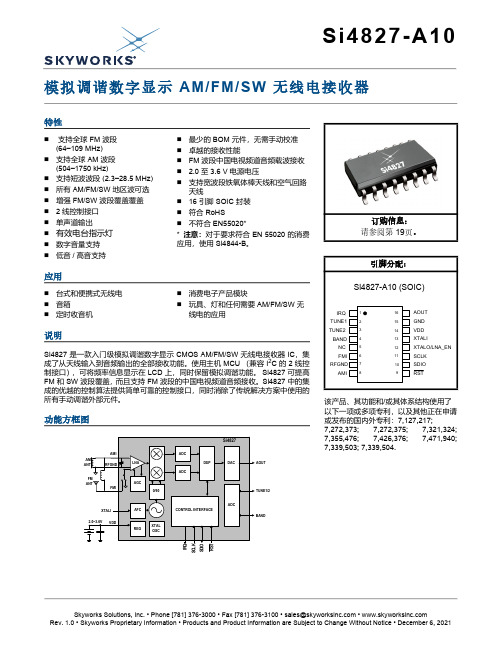
SkyworksSolutions,Inc.•Phone[781]376-3000•Fax[781]376-3100•*********************•Si4827-A10模拟调谐数字显示 AM/FM/SW 无线电接收器特性所有手动调谐外部元件。
功能方框图⏹ 支持全球 FM 波段(64–109MHz)⏹支持全球 AM 波段(504–1750kHz)⏹支持短波波段 (2.3–28.5MHz)⏹所有 AM/FM/SW 地区波可选⏹增强 FM/SW 波段覆盖覆盖⏹ 2 线控制接口⏹单声道输出⏹有效电台指示灯⏹数字音量支持⏹最少的 BOM 元件,无需手动校准⏹卓越的接收性能⏹FM 波段中国电视频道音频载波接收⏹ 2.0 至 3.6V 电源电压⏹支持宽波段铁氧体棒天线和空气回路天线⏹16 引脚 SOIC 封装⏹符合 RoHS⏹不符合 EN55020**注意:对于要求符合 EN 55020 的消费应用,使用 Si4844-B 。
该产品、其功能和/或其体系结构使用了以下一项或多项专利,以及其他正在申请或发布的国内外专利:7,127,217;7,272,373; 7,272,375; 7,321,324;7,355,476; 7,426,376; 7,471,940;7,339,503; 7,339,504.订购信息:请参阅第 19页。
Si4827-A102SkyworksSolutions,Inc.•Phone[781]376-3000•Fax[781]376-3100•*********************•Si4827-A10SkyworksSolutions,Inc.•Phone[781]376-3000•Fax[781]376-3100•*********************• 3T ABLE OF C ONTENTSSectionPage1. Electrical Specifications . . . . . . . . . . . . . . . . . . . . . . . . . . . . . . . . . . . . . . . . . . . . . . . . . . .42. Typical Application Schematic . . . . . . . . . . . . . . . . . . . . . . . . . . . . . . . . . . . . . . . . . . . . .113. Bill of Materials . . . . . . . . . . . . . . . . . . . . . . . . . . . . . . . . . . . . . . . . . . . . . . . . . . . . . . . . .124. Functional Description . . . . . . . . . . . . . . . . . . . . . . . . . . . . . . . . . . . . . . . . . . . . . . . . . . .134.1. Overview . . . . . . . . . . . . . . . . . . . . . . . . . . . . . . . . . . . . . . . . . . . . . . . . . . . . . . . . . .134.2. FM Receiver . . . . . . . . . . . . . . . . . . . . . . . . . . . . . . . . . . . . . . . . . . . . . . . . . . . . . . .144.3. AM Receiver . . . . . . . . . . . . . . . . . . . . . . . . . . . . . . . . . . . . . . . . . . . . . . . . . . . . . . .144.4. SW Receiver . . . . . . . . . . . . . . . . . . . . . . . . . . . . . . . . . . . . . . . . . . . . . . . . . . . . . . .144.5. Frequency Tuning . . . . . . . . . . . . . . . . . . . . . . . . . . . . . . . . . . . . . . . . . . . . . . . . . . .144.6. Band Select . . . . . . . . . . . . . . . . . . . . . . . . . . . . . . . . . . . . . . . . . . . . . . . . . . . . . . . .144.7. Bass and Treble . . . . . . . . . . . . . . . . . . . . . . . . . . . . . . . . . . . . . . . . . . . . . . . . . . . .154.8. Volume Control . . . . . . . . . . . . . . . . . . . . . . . . . . . . . . . . . . . . . . . . . . . . . . . . . . . . .154.9. High Fidelity DAC . . . . . . . . . . . . . . . . . . . . . . . . . . . . . . . . . . . . . . . . . . . . . . . . . . .154.10. Soft Mute . . . . . . . . . . . . . . . . . . . . . . . . . . . . . . . . . . . . . . . . . . . . . . . . . . . . . . . . .154.11. Reference Clock . . . . . . . . . . . . . . . . . . . . . . . . . . . . . . . . . . . . . . . . . . . . . . . . . . .154.12. Reset, Powerup, and Powerdown . . . . . . . . . . . . . . . . . . . . . . . . . . . . . . . . . . . . . .154.13. Memorizing Status . . . . . . . . . . . . . . . . . . . . . . . . . . . . . . . . . . . . . . . . . . . . . . . . .154.14. Programming with Commands . . . . . . . . . . . . . . . . . . . . . . . . . . . . . . . . . . . . . . . .155. Commands and Properties . . . . . . . . . . . . . . . . . . . . . . . . . . . . . . . . . . . . . . . . . . . . . . . .166. Pin Descriptions: Si4827-A10 . . . . . . . . . . . . . . . . . . . . . . . . . . . . . . . . . . . . . . . . . . . . . .187. Ordering Guide . . . . . . . . . . . . . . . . . . . . . . . . . . . . . . . . . . . . . . . . . . . . . . . . . . . . . . . . . .198. Package Outline: Si4827-A10 . . . . . . . . . . . . . . . . . . . . . . . . . . . . . . . . . . . . . . . . . . . . . .209. PCB Land Pattern: Si4827-A10 . . . . . . . . . . . . . . . . . . . . . . . . . . . . . . . . . . . . . . . . . . . . .2110. Top Markings . . . . . . . . . . . . . . . . . . . . . . . . . . . . . . . . . . . . . . . . . . . . . . . . . . . . . . . . . .2210.1. Si4827-A10 Top Marking . . . . . . . . . . . . . . . . . . . . . . . . . . . . . . . . . . . . . . . . . . . .2210.2. Top Marking Explanation . . . . . . . . . . . . . . . . . . . . . . . . . . . . . . . . . . . . . . . . . . . .2211. Additional Reference Resources . . . . . . . . . . . . . . . . . . . . . . . . . . . . . . . . . . . . . . . . . .23Document Change List . . . . . . . . . . . . . . . . . . . . . . . . . . . . . . . . . . . . . . . . . . . . . . . . . . . . .24Si4827-A104SkyworksSolutions,Inc.•Phone[781]376-3000•Fax[781]376-3100•*********************•1. Electrical SpecificationsTable 1. Recommended Operating Conditions 1,2ParameterSymbol Test ConditionMin Typ Max Unit Supply Voltage 3V DD 2.0— 3.6V Power Supply Powerup Rise Time V DDRISE10——µs Ambient Temperature RangeT A2570°CNotes:1.Typical values in the data sheet apply at V DD =3.3V and 25°C unless otherwise stated.2. All minimum and maximum specifications in the data sheet apply across the recommended operating conditions forminimum V DD =2.7V.3. Operation at minimum V DD is guaranteed by characterization when V DD voltage is ramped down to 2.0V. Partinitialization may become unresponsive below 2.3V.Table 2. DC Characteristics(V DD =2.7 to 3.6V, TA =0 to 70°C)ParameterSymbolTest ConditionMinTypMaxUnitFM ModeSupply Current *I FM—21.0—mAAM/SW ModeSupply Current *I AM—20.0—mASupplies and InterfaceV DD Powerdown CurrentI DDPD—10—µA*Note: Specifications are guaranteed by characterization.Si4827-A10SkyworksSolutions,Inc.•Phone[781]376-3000•Fax[781]376-3100•*********************• 5Figure 1.Reset TimingTable 3. Reset Timing Characteristics(V DD = 2.7 to 3.6V, TA = 0 to 70°C)ParameterSymbol Min Typ Max Unit RSTB Pulse Widtht PRST 100——µs 2-wire Bus Idle Time After RSTB Risest SDIO 100——µs 2-wire Bus Idle Time Before RSTB Rises, and VDD Valid Time Before RSTB Risest SRST 100——µs RSTB Low Time Before VDD Becomes Invalidt RRST——µsNotes:1.RSTB must be held low for at least 100µs after the voltage supply has been ramped up.2. RSTB needs to be asserted (pulled low) prior to the supply voltage being ramped down.RSTBVDDSDIOSCLKSi4827-A106SkyworksSolutions,Inc.•Phone[781]376-3000•Fax[781]376-3100•*********************•Table 4. 2-Wire Control Interface Characteristics 1,2,3(V DD =2.7 to 3.6V, T A =0 to 70°C)ParameterSymbol Test ConditionMin Typ Max Unit SCLK Frequency f SCLK 0—400kHz SCLK Low Time t LOW 1.3——µs SCLK High Timet HIGH 0.6——µs SCLK Input to SDIO ↓ Setup (START)t SU:STA 0.6——µs SCLK Input to SDIO ↓ Hold (START)t HD:STA 0.6——µs SDIO Input to SCLK ↑ Setup t SU:DAT 100——ns SDIO Input to SCLK ↓ Hold 4,5t HD:DAT 0—900ns SCLK input to SDIO ↑ Setup (STOP)t SU:STO 0.6——µs STOP to START Time t BUF 1.3——µs SDIO Output Fall Timet f:OUT—250nsSDIO Input, SCLK Rise/Fall Timet f:IN t r:IN—300nsSCLK, SDIO Capacitive Loading C b ——50pF Input Filter Pulse Suppressiont SP——50nsNotes:1.When V D =0V, SCLK and SDIO are low impedance.2. When selecting 2-wire mode, the user must ensure that a 2-wire start condition (falling edge of SDIO while SCLK ishigh) does not occur within 300ns before the rising edge of RST.3. When selecting 2-wire mode, the user must ensure that SCLK is high during the rising edge of RST, and stays highuntil after the first start condition.4. The Si4827 delays SDIO by a minimum of 300ns from the V IH threshold of SCLK to comply with the minimum t HD:DATspecification.5. The maximum t HD:DAT has only to be met when f SCLK =400kHz. At frequencies below 400kHz, t HD:DAT may beviolated as long as all other timing parameters are met.200.1C b1pF----------+200.1C b1pF----------+Si4827-A10SkyworksSolutions,Inc.•Phone[781]376-3000•Fax[781]376-3100•*********************• 7Figure 2.2-Wire Control Interface Read and Write Timing ParametersFigure 3.2-Wire Control Interface Read and Write Timing DiagramTable 5. FM Receiver Characteristics 1,2(V DD =2.7 to 3.6V, TA =0 to 70°C)ParameterSymbol Test ConditionMin Typ Max Unit Input Frequencyf RF64—109MHz Sensitivity with Headphone Network 3(S+N)/N = 26 dB —4.0—µV EMFNotes:1.Additional testing information is available in “AN603: Si4822/26/27/40/44-DEMO Board Test Procedure”Volume =maximum for all tests. Tested at RF =98.1MHz.2. To ensure proper operation and receiver performance, follow the guidelines in “AN602: Si4822/26/27/40/44 Antenna,Schematic, Layout, and Design Guidelines.” Skyworks will evaluate schematics and layouts for qualified customers.3. Frequency is 64~109MHz.4. Guaranteed by characterization.5. V EMF =1 mV.6. F MOD =1kHz, MONO, and L =R unless noted otherwise.7. ∆f =22.5kHz.8. |f 2 – f 1| > 2MHz, f 0=2x f 1 – f 2.9. B AF =300Hz to 15kHz, A-weighted.10. At A OUT pin.11. ∆f =75 kHz.12. Tested in Digital Volume Mode.SCLK70%30%SDIO70%30%STARTSTOP t f:INt r:INt LOWt HIGHt HD:STAt SU:STA t t t SU:DATt r:INHD:DATf:IN, t f:OUTSi4827-A108SkyworksSolutions,Inc.•Phone[781]376-3000•Fax[781]376-3100•*********************•LNA Input Resistance 4,5—4—k ΩLNA Input Capacitance 4,5—5—pF AM Suppression 4,5,6,7m = 0.3—50—dB Input IP34,8—105—dBµV EMFAdjacent Channel Selectivity 4±200 kHz —45—dB Alternate Channel Selectivity 4±400 kHz —60—dB Audio Output Voltage 5,6,7,12—72—mV RMS Audio Mono S/N 5,6,7,9,10—45—dB Audio Frequency Response Low 4–3dB ——30Hz Audio Frequency Response High 4–3dB 15——kHz Audio THD 5,6,11—0.10.5%Audio Output Load Resistance 4,10R L Single-ended 10——k ΩAudio Output Load Capacitance 4,10C LSingle-ended——50pFTable 5. FM Receiver Characteristics 1,2 (Continued)(V DD =2.7 to 3.6V, TA =0 to 70°C)ParameterSymbolTest ConditionMin Typ Max Unit Notes:1.Additional testing information is available in “AN603: Si4822/26/27/40/44-DEMO Board Test Procedure”Volume =maximum for all tests. Tested at RF =98.1MHz.2. To ensure proper operation and receiver performance, follow the guidelines in “AN602: Si4822/26/27/40/44 Antenna,Schematic, Layout, and Design Guidelines.” Skyworks will evaluate schematics and layouts for qualified customers.3. Frequency is 64~109MHz.4. Guaranteed by characterization.5. V EMF =1 mV.6. F MOD =1kHz, MONO, and L =R unless noted otherwise.7. ∆f =22.5kHz.8. |f 2 – f 1| > 2MHz, f 0=2x f 1 – f 2.9. B AF =300Hz to 15kHz, A-weighted.10. At A OUT pin.11. ∆f =75 kHz.12. Tested in Digital Volume Mode.Si4827-A10SkyworksSolutions,Inc.•Phone[781]376-3000•Fax[781]376-3100•*********************• 9Table 6. AM/SW Receiver Characteristics 1, 2(V DD = 2.7 to 3.6 V, TA = 0 to 70 °C)ParameterSymbol Test Condition Min Typ Max Unit Input Frequencyf RFMedium Wave (AM)504— 1750kHz Short Wave (SW)2.3—28.5MHz Sensitivity 3,4,5(S+N)/N = 26 dB — 30—µV EMF Large Signal Voltage Handling 5THD < 8%— 300— mV RMS Power Supply Rejection Ratio 5ΔV DD =100 mV RMS , 100 Hz— 40— dB Audio Output Voltage 3,6,8— 54— mV RMS Audio S/N 3,4,6— 45— dB Audio THD 3,6— 0.1— %Antenna Inductance 5,7180—450µHNotes:1.Additional testing information is available in “AN603: Si4822/26/27/40/44 DEMO Board Test Procedure.”Volume =maximum for all tests. Tested at RF =6MHz.2. To ensure proper operation and receiver performance, follow the guidelines in “AN602: Si4822/26/27/40/44 Antenna,Schematic, Layout, and Design Guidelines.” Skyworks will evaluate schematics and layouts for qualified customers.3. FMOD =1kHz, 30% modulation, 2kHz channel filter.4. B AF =300Hz to 15kHz, A-weighted.5. Guaranteed by characterization.6. V IN =5mVrms.7. Stray capacitance on antenna and board must be <10pF to achieve full tuning range at higher inductance levels.8. Tested in Digital Volume Mode.Table 7. Reference Clock and Crystal Characteristics(V DD = 2.7 to 3.6V, T A = 0 to 70°C)ParameterSymbolTest Condition MinTypMaxUnitReference ClockXTALI Supported Reference Clock Frequencies*31.13032.76840,000kHz Reference Clock Frequency Tolerance for XTALI–100—100ppmREFCLK_PRESCALE 1—4095REFCLK31.13032.76834.406kHz Crystal OscillatorCrystal Oscillator Frequency —32.768—kHz Crystal Frequency Tolerance –100—100ppm Board Capacitance——3.5pF*Note: The Si4827-A10 divides the RCLK input by REFCLK_PRESCALE to obtain REFCLK. There are some RCLKfrequencies between 31.130 kHz and 40 MHz that are not supported. For more details, see Table 9 of "AN610: Si48xx ATDD Programming Guide.”Si4827-A1010SkyworksSolutions,Inc.•Phone[781]376-3000•Fax[781]376-3100•*********************•Table 8. Thermal ConditionsParameterSymbol Min Typ Max Unit Thermal Resistance* JA —80—°C/W Ambient Temperature T A 02570°C Junction TemperatureT J——77°C*Note: Thermal resistance assumes a multi-layer PCB with the exposed pad soldered to a topside PCB pad.Table 9. Absolute Maximum Ratings 1,2ParameterSymbol Value Unit Supply Voltage V DD –0.5 to 5.8V Input Current 3I IN 10mA Operating Temperature T OP –40 to 95°C Storage Temperature T STG–55 to 150°C RF Input Level 40.4V PKNotes:1.Permanent device damage may occur if the above Absolute Maximum Ratings are exceeded. Functional operationshould be restricted to the conditions as specified in the operational sections of this data sheet. Exposure beyond recommended operating conditions for extended periods may affect device reliability.2. The Si4827-A10 devices are high-performance RF integrated circuits with certain pins having an ESD rating of<2kV HBM. Handling and assembly of these devices should only be done at ESD-protected workstations.3. For input pins RST, SDIO, SCLK, XTALO/LNA_EN, XTALI, BAND, TUNE2, TUNE1 and IRQ.4. At RF input pins, FMI, and AMI.2. Typical Application SchematicNotes:1.Place C4 close to V DD and GND pins.2. All grounds connect directly to GND plane on PCB.3. Pin 5 leave floating.4. To ensure proper operation and receiver performance, follow the guidelines in “AN602: Si4822/26/27/40/44 Antenna,Schematic, Layout, and Design Guidelines.” Skyworks will evaluate the schematics and layouts for qualified customers.5. Pin 6 connects to the FM antenna interface and pin 8 connects to the AM antenna interface.6. Place Si4827 as close as possible to antenna jack and keep the FMI and AMI traces as short as possible.7. Recommend keeping the AM ferrite loop antenna at least 5 cm away from the Si4827.8. Keep the AM ferrite loop antenna away from MCU, audio amplifier, and other circuits which have AM interference.9. Place the transformer T1 away from any sources of interference and even away from the I/O signals of the Si4827.3. Bill of MaterialsTable 10. Si4827-A10 Bill of MaterialsComponent(s)Value/Description Supplier C1Reset capacitor 0.1µF, ±20%, Z5U/X7R MurataC4Supply bypass capacitor, 0.1µF, ±20%, Z5U/X7R MurataC5Coupling capacitor, 0.47µF, ±20%, Z5U/X7R MurataB1Ferrite bead 2.5k/100MHz MurataVR1Variable resistor (POT), 100kΩ, ±10%KennonU1Si4827-A AM/FM/SW Analog Tune Digital Display Radio Tuner SkyworksANT1Ferrite stick,180–450μH JiaxinOptional ComponentsC2, C3Crystal load capacitors, 22pF, ±5%, COGVenkel(Optional: for crystal oscillator option)Y132.768kHz crystal (Optional: for crystal oscillator option)Epson or equivalent ANT2Air loop antenna, 10–20μH VariousS1Band switch Any, depends oncustomer R1Resistor, 203kΩ, ±1%VenkelR2Resistor, 50kΩ, ±1%,VenkelR3Resistor, 180kΩ, ±1%VenkelR4Resistor, 67kΩ, ±1%Venkel4. Functional DescriptionFigure4.Si4827-A10 Functional Block Diagram4.1. OverviewThe Si4827-A10 is the entry level analog-tuned digital-display digital CMOS AM/FM/SW radio receiver IC that integrates the complete receiver function from antenna input to audio output. Working with an external MCU with LCD/LED driver, Si4827 can output the AM/FM/SW frequencies and band and volume information to display on LCD/LED, while using a simple potentiometer at the front end for analog-tune. Leveraging Skyworks' proven and patented digital low intermediate frequency (low-IF) receiver architecture, the Si4827 delivers superior RF performance and interference rejection in AM, FM and SW bands. Additionally, the digital core provides advanced audio conditioning for all environments, removing pops, clicks, and loud static in variable signal conditions. The superior control algorithm integrated in Si4827 provides easy and reliable control interface while eliminating all the manual tuned external components used in traditional solutions.Like other successful audio products from Skyworks, Si4827 offers unmatched integration and PCB space savings with minimum external components and a small board area on a single side PCB. The high integration and complete system production test simplifies design-in, increases system quality, and improves manufacturability. The receiver has very low power consumption, runs off two AAA batteries, and delivers the performance benefits of high performance digital radio experience with digital display to the legacy analog-tuned radio market.The Si4827 provides good flexibility in using the chip. The frequency range of FM/AM/SW bands, de-emphasis value, AM tuning step, and AM soft mute level/rate can be either configured by the MCU or by using external hardware to make a selection. The reference clock of the FM tuner can be provided by either the crystal or by the host MCU within tolerance. The Si4827 also has flexibility in selecting bands and configuring band properties, enabling masked Host MCU for multiple projects, and reducing the cost of development. Four tuning preferences are available to meet different tuning preference requirements.AOUT TUNE1/2 BAND4.2. FM ReceiverThe Si4827-A10 integrates a low noise amplifier(LNA) supporting the worldwide FM broadcast band (64to 109MHz) and the TV audio stations within the frequency range in China area are also supported. The FM band can also be configured to be wider range such as 64–108 MHz in one band.Pre-emphasis and de-emphasis is a technique used by FM broadcasters to improve the signal-to-noise ratio of FM receivers by reducing the effects of high frequency interference and noise. When the FM signal is transmitted, a pre-emphasis filter is applied to accentuate the high audio frequencies. All FM receivers incorporate a de-emphasis filter which attenuates high frequencies to restore a flat frequency response. Two time constants are used in various regions. The de-emphasis time constant can be chosen to be 50 or 75μs. Refer to "AN602: Si4822/26/27/40/44 Antenna, Schematic, Layout, and Design Guidelines."4.3. AM ReceiverThe highly integrated Si4827-A10 supports worldwide AM band reception from 504 to 1750kHz with five sub-bands using a digital low-IF architecture with a minimum number of external components and no manual alignment required. This patented architecture allows for high-precision filtering, offering excellent selectivity and SNR with minimum variation across the AM band. Similar to the FM receiver, the Si4827-A10 optimizes sensitivity and rejection of strong interferers, allowing better reception of weak stations.To offer maximum flexibility, the receiver supports a wide range of ferrite loop sticks from 180–450μH. An air loop antenna is supported by using a transformer to increase the effective inductance from the air loop. Using a 1:5 turn ratio inductor, the inductance is increased by 25 times and easily supports all typical AM air loop antennas, which generally vary between 10 and 20μH.A 9, 10kHz tuning step can be chosen by the external resistor or host MCU according to the different regions, and AM soft mute level can be programmed by the host MCU to have different tuning experiences. One of the AM bands can be configured as a universal AM band that simultaneously supports 9kHz and 10kHz channel spaces for all regional AM standards. Refer to “AN610: Si48xx ATDD Programming Guide” and "AN602: Si4822/26/27/40/44 Antenna, Schematic, Layout, and Design Guidelines" for more details.4.4. SW ReceiverThe Si4827 supports short wave band receptions from 2.3 to 28.5MHz in 5kHz step size increments. It can also be configured to have wide SW band that can be used in SW radio with 1 or 2 SW bands. The Si4827 supports extensive short wave features such as minimal discrete components and no factory adjustments. The Si4827 supports using the FM antenna to capture short wave signals. Refer to “AN610: Si48xx ATDD Programming Guide”and "AN602: Si4822/26/27/40/44 Antenna, Schematic, Layout, and Design Guidelines" for more details.4.5. Frequency TuningA valid channel can be found by tuning the potentiometer that is connected to the TUNE1 and TUNE2 pin of the Si4827-A10 chip.To offer easy tuning, the Si4827-A10 also outputs the tuned information to the MCU with LCD/LED driver to display. It will light up the icon on display if the RF signal quality passes a certain threshold when tuned to a valid station. Refer to "AN610: Si48xx ATDD Programming Guide" for more details.4.6. Band SelectThe Si4827-A10 supports worldwide AM band with five sub-bands, US/Europe/Japan/China FM band with five sub-bands, and SW band with 16 sub-bands. Si4827-A10 provides the flexibility to configure the band and band properties at either the MCU side or the tuner side, enabling masked MCU for multiple projects. For details on band selection, refer to "AN602: Si4822/26/27/40/44 Antenna, Schematic, Layout, and Design Guidelines" and "AN610: Si48xx ATDD Programming Guide".4.7. Bass and TrebleThe Si4827-A10 supports Bass/Treble tone control for superior sound quality. The Si4827-A10 can be set to be default normal, or programmed by the host MCU I2C-compatible 2-wire mode. FM has nine levels Bass/Treble effect and AM/SW has seven levels Bass/Treble effect. For further configuration details, refer to "AN610: Si48xx ATDD Programming Guide". 4.8. Volume ControlThe Si4827-A10 not only allows users to use the traditional PVR wheel volume control through an external speaker amplifier, it also supports digital volume control programmed by the host MCU. Si4827-A10 can be programmed to be Bass/Treble mode only or digital volume mode only; it can also be programmed to have the digital volume coexist with Bass/Treble in two modes. Refer to "AN610: Si48xx ATDD Programming Guide" and "AN602: Si4822/26/27/40/44 Antenna, Schematic, Layout, and Design Guidelines" for more details.4.9. High Fidelity DACHigh-fidelity digital-to-analog converters (DACs)drive analog audio signals onto the AOUT pin. The audio output may be muted.4.10. Soft MuteThe soft mute feature is available to attenuate the audio outputs and minimize audible noise in very weak signal conditions. Advanced algorithm is implemented to get a better analog tuning experience. The soft mute feature is triggered by the SNR metric. The SNR threshold for activating soft mute is programmable, as are soft mute attenuation levels and attack and decay rates.4.11. Reference ClockThe Si4827-A10 supports RCLK input (to XTALI pin) with the spec listed in Table7. It can be shared with the host MCU to save extra crystal.An onboard crystal oscillator is available to generate the 32.768kHz reference when an external crystal and load capacitors are provided. Refer to "AN602: Si4822/26/27/40/44 Antenna, Schematic, Layout, and Design Guidelines" for more details.4.12. Reset, Powerup, and Powerdown Setting the RSTB pin low will disable analog and digital circuitry, reset the registers to their default settings, and disable the bus. Setting the RSTB pin high will bring the device out of reset.Figure1 shows typical reset, startup, and shutdown timings for the Si4827. RSTB must be held low (asserted) during any power supply transitions and kept asserted as specified in Figure1 after the power supplies are ramped up and stable. Failure to assert RSTB as indicated here may cause the device to malfunction and may result in permanent device damage.A powerdown mode is available to reduce power consumption when the part is idle. Putting the device in powerdown mode will disable analog and digital circuitry while keeping the bus active.4.13. Memorizing StatusThe Si4827-A10 provides the feature to memorize status from the last power down with a simple design on PCB, including frequency of the FM/AM/SW station. Refer to "AN602: Si4822/26/27/40/44 Antenna, Schematic, Layout, and Design Guidelines" for details.4.14. Programming with CommandsTo ease development time and offer maximum customization, the Si4827 provides a simple yet powerful software interface to program the receiver. The device is programmed using commands, arguments, properties, and responses.To perform an action, the user writes a command byte and associated arguments, causing the chip to execute the given command. Commands control an action such as powerup the device, shut down the device, or get the current tuned frequency. Arguments are specific to a given command and are used to modify the command. Properties are a special command argument used to modify the default chip operation and are generally configured immediately after powerup. Examples of properties are de-emphasis level and soft mute attenuation threshold.Responses provide the user information and are echoed after a command and associated arguments are issued. All commands provide a 1-byte status update, indicating interrupt and clear-to-send status information. For a detailed description of the commands and properties for the Si4827, see "AN610: Si48xx ATDD Programming Guide".5. Commands and PropertiesTable 11. Si4827-A10 FM Receiver Command Summary Cmd Name Description0xE0ATDD_GET_STATUS Get tune freq, band and etc., status of the device.0xE1ATDD_POWER_UP Power up device, band selection, and band properties setup.0xE2ATDD_AUDIO_MODE Audio output mode: get/set audio mode and settings.0x10GET_REV Returns the revision information of the device.0x11POWER_DOWN Power down device.0x12SET_PROPERTY Sets the value of a property.0x13GET_PROPERTY Retrieve a property's value.Note:The Si4827 has its own power up and get status commands which are different from previous si47xx tuner parts. To differentiate, we use "ATDD_POWER_UP" and ATDD_GET_STATUS to denote the ATDD specific commands instead of the general si47xx "POWER_UP" and "STATUS" commands.Table 12. Si4827-A10 FM Receiver Property SummaryProp Name Description Default 0x0201REFCLK_FREQ Sets frequency of reference clock in Hz.The range is 31130 to 34406Hz, or 0 to disable the AFC. Default is32768Hz.0x8000 0x0202REFCLK_PRESCALE Sets the prescaler value for RCLK input.0x0001 0x1100FM_DEEMPHASIS Sets deemphasis time constant. Default is 75μs.0x0002 0x1300FM_SOFT_MUTE_RATE Sets the attack and decay rates when entering and leaving soft mute.0x00400x1301FM_SOFT_MUTE_SLOPE Configures attenuation slope during soft mute in dB attenuation perdB SNR below the soft mute SNR threshold. Default value is 2.0x00020x1302FM_SOFT_MUTE_MAX_ATTENUATION Sets maximum attenuation during soft mute (dB). Set to 0 to disablesoft mute. Default is 16dB.0x00100x1303FM_SOFT_MUTE_SNR_THRESHOLDSets SNR threshold to engage soft mute. Default is 4dB.0x0004 0x4000RX_VOLUME Sets the output volume.0x003F0x4001RX_HARD_MUTE Mutes the audio output. L and R audio outputs may be muted inde-pendently.0x0000 0x4002RX_BASS_TREBLE Sets the output bass/treble level.0x0004 0x4003RX_ACTUAL_VOLUME Read the actual output volume.0x003F。
SKY65137-11;中文规格书,Datasheet资料
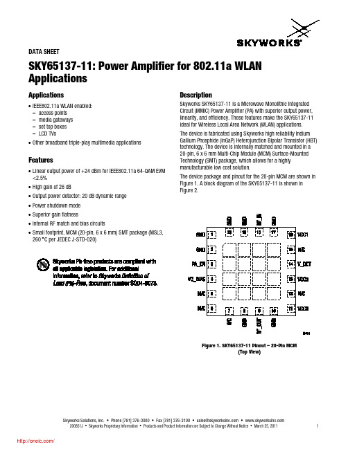
DATA SHEETSKY65137-11: Power Amplifier for 802.11a WLAN ApplicationsApplications•IEEE802.11a WLAN enabled:−access points−media gateways−set top boxes−LCD TVs•O ther broadband triple-play multimedia applicationsFeatures•Linear output power of +24 dBm for IEEE802.11a64-QAM EVM <2.5%•High gain of 26dB•Output power detector: 20 dB dynamic range•Power shutdown mode•Superior gain flatness•Internal RF match and bias circuits•Small footprint, MCM (20-pin, 6x 6 mm) SMT package (MSL3, 260 °C per JEDEC J-STD-020)DescriptionSkyworks SKY65137-11is a Microwave Monolithic Integrated Circuit (MMIC) Power Amplifier (PA) with superior output power, linearity, and efficiency. These features make the SKY65137-11 ideal for Wireless Local Area Network (WLAN) applicat ions.The device is fabricated using Skyworks high reliability Indium Gallium Phosphide (InGaP) Heterojunction Bipolar Transistor (HBT) technology. The device is internally matched and mounted in a 20-pin, 6x 6 mm Multi-Chip Module (MCM) Surface-Mounted Technology (SMT) package, which allows for a highly manufacturable low cost solution.The device package and pinout for the 20-pin MCM are shown in Figure 1. A block diagram of the SKY65137-11is shown in Figure2.Figure 1. SKY65137-11 Pinout – 20-Pin MCM(Top View)Skyworks Solutions, Inc. • Phone [781] 376-3000 • Fax [781] 376-3100 • sales@ • 200851J•Skyworks Proprietary I nformation • Products and Product Information are Subject to Change Without Notice • March 25, 20111DATA SHEET • SKY65137-11 WLAN PASkyworks Solutions, Inc. • Phone [781] 376-3000 • Fax [781] 376-3100 • sales@ • www.skyw 2March 25, 2011 • Skyworks Proprietary I nformation • Products and Product Information are Subject to Change Without Notice • 200851JFigure 2. SKY65137-11 Block DiagramTechnical DescriptionThe SKY65137-11 PA contains all of the needed RF matching and DC biasing circuits. The device also provides an output power detector voltage.The SKY65137-11 is a three -stage, HBT InGaP device optimized for high linearity and power efficiency. These features make the device suitable for wideband digital applications, where PA linearity and power consumption are of critical importance (e.g., WLANs).The device has been characterized with the highest specified data rates for IEEE 802.11a (54 Mbps). Under these stringent testconditions, the device exhibits excellent spectral purity and power efficiency.Electrical and Mechanical SpecificationsSignal pin assignments and functional pin descriptions are described in Table 1. The absolute maximum ratings of theSKY65137-11 are provided in Table 2. Electrical specifications are provided in Table 3.Typical performance characteristics of the SKY65137-11 are illustrated in Figures 3 through 19.DATA SHEET • SKY65137-11 WLAN PAparameters set at or below their nominal value. Exceeding any of the limits listed here may result in permanent damage to the device.Note 2:Evaluation Board supply voltage levels can be different. Refer to the Evaluation Board schematic diagram in Figure 21.CAUTION: Although this device is designed to be as robust as possible, Electrostatic Discharge (ESD) can damage this device. This device must be protected at all times from ESD. Static charges may easily produce potentials of several kilovolts on the human body or equipment, which can discharge without detection. Industry-standard ESD precautions should be used at all times.Note 1:Evaluation Board supply voltage levels can be different. Refer to the Evaluation Board schematic diagram in Figure 21.Table 4. SKY65137-11 Electrical Specifications (1 of 2) (Note 1)CSkyworks Solutions, Inc. • Phone [781] 376-3000 • Fax [781] 376-3100 • sales@ • 200851J• Skyworks Proprietary I nformation • Products and Product Information are Subject to Change Without Notice • March 25, 20113DATA SHEET • SKY65137-11 WLAN PASkyworks Solutions, Inc. • Phone [781] 376-3000 • Fax [781] 376-3100 • sales@ • www.skyw 4March 25, 2011 • Skyworks Proprietary I nformation • Products and Product Information are Subject to Change Without Notice • 200851JTable 4. SKY65137-11 Electrical Specifications (1 of 2) (Note 1)CNote 1: Performance is guaranteed only under the conditions listed in this Table.Typical Performance Characteristics(VCC1 = VCC2 = VCC3 = VC_BIAS = 5 V, PA_EN = 3.3 V Static, T C = +25 °C, Test Frequency = 5.75 GHz, Unless Otherwise Noted)Figure 3. Low Band EVM vs Output PowerFigure 5. Low Band Detector Voltage vs Output PowerFigure 7. Supply Current vs Output Power, Modulated InputFigure 4. High Band EVM vs Output PowerFigure 6. High Band Detector Voltage vs Output PowerFigure 8. Supply Current vs Output Power, CW InputDATA SHEET • SKY65137-11 WLAN PASkyworks Solutions, Inc. • Phone [781] 376-3000 • Fax [781] 376-3100 • sales@ • 200851J • Skyworks Proprietary I nformation • Products and Product Information are Subject to Change Without Notice • March 25, 20115Figure 9. EVM vs Output Power Over VoltageFigure 11. Small Signal Gain vs Frequency Over VoltageFigure 13. Typical Spectral Response With 802.11a 65-QAMOFDM Signal Over Output Power LevelFigure 10. EVM vs Output Power Over TemperatureFigure 12. Small Signal Gain vs Frequency Over TemperatureFigure 14. Second Harmonic vs Output PowerDATA SHEET • SKY65137-11 WLAN PASkyworks Solutions, Inc. • Phone [781] 376-3000 • Fax [781] 376-3100 • sales@ • www.skyw 6March 25, 2011 • Skyworks Proprietary I nformation • Products and Product Information are Subject to Change Without Notice • 200851JFigure 15. Detector Voltage vs Output Power Over TemperatureFigure 17. Noise Figure vs FrequencyFigure 19. Power-Down TimeFigure 16. Detector Voltage vs Output Power Over VoltageFigure 18. Start-Up TimeDATA SHEET • SKY65137-11 WLAN PASkyworks Solutions, Inc. • Phone [781] 376-3000 • Fax [781] 376-3100 • sales@ • 200851J • Skyworks Proprietary I nformation • Products and Product Information are Subject to Change Without Notice • March 25, 20117Evaluation Board DescriptionThe SKY65137-11 Evaluation Board is used to test theperformance of the SKY65137-11 WLAN PA. An assembly drawing for the Evaluation Board is shown in Figure 20 and the layer detail is provided in Figure 21. Layer detail physical characteristics are noted in Figure 22. A schematic diagram of the SKY65137-11 Evaluation Board is shown in Figure 23.Circuit Design ConsiderationsThe following design considerations are general in nature and must be followed regardless of final use or configuration 1. Paths to ground should be made as short as possible. 2. The ground pad of the SKY65137-11 has special electrical and thermal grounding requirements. This pad is the main thermal conduit for heat dissipation. Since the circuit board acts as the heat sink, it must shunt as much heat as possible from the device. Therefore, design the connection to the ground pad to dissipate the maximum wattage produced by the circuit board. Multiple vias to the grounding layer are required . 3. Bypass capacitors should be used on the DC supply lines. The V CC lines may be connected after the RF bypass anddecoupling capacitors to provide better isolation between each V CC line. Refer to Figure 23 for further details. 4. The RF lines should be well separated from each other with solid ground in between traces to maximize input -to-output isolation. NOTE: A poor connection between the slug and ground increasesjunction temperature (T J ), which reduces the lifetime of the device. Refer to the Skyworks Application Note, “PCB Design Guidelines for High Power Dissipation Packages” (document number 201211) for further information.Evaluation Board Test ProcedureStep 1: Connect a +5 V supply to the VCC1, VCC2, VCC3, andVC_BIAS pins. Connect the PA_ENB pin to a separate supply. If available, enable the current limiting function of the power supply to 1000 mA. Step 2: If desired, connect a voltage meter to the V_DET pin. Step 3: Connect a signal generator to the RF signal input port. Setit to the desired RF frequency at a power level of–15 dBm or less to the Evaluation Board. DO NOT enable the RF signal. Step 4: Connect a spectrum analyzer or vector signal analyzer tothe RF signal output port. Add attenuation as needed to protect the analyzer. Step 5: On startup, turn on the VCC1, VCC2, VCC3, and VC_BIASlines first. Then turn on the PA_ENB line. Finally, turn on the RF input. Make sure to keep the initial input power to the PA at –20 dBm and gradually increase to the desired output power level. Step 6: Take measurements.Step 7: On power down, turn off the RF input first. Then turn offthe PA_ENB line. Finally, turn off the VCC1, VCC2, VCC3, and VC_BIAS lines.Package DimensionsThe PCB layout footprint for the SKY65137-11 is provided in Figure 22. Package dimensions for the 20-pin MCM are shown in Figure 23, and tape and reel dimensions are provided in Figure 24.Package and Handling InformationSince the device package is sensitive to moisture absorption, it is baked and vacuum packed before shipping. Instructions on the shipping container label regarding exposure to moisture after the container seal is broken must be followed. Otherwise, problems related to moisture absorption may occur when the part is subjected to high temperature during solder assembly. The SKY65137-11 is rated to Moisture Sensitivity Level 3 (MSL3) at 260 °C. It can be used for lead or lead -free soldering. For additional information, refer to Skyworks Application Note, PCB Design and SMT Assembly/Rework Guidelines for MCM-L Packages , document number 101752.Care must be taken when attaching this product, whether it is done manually or in a production solder reflow environment. Production quantities of this product are shipped in a standard tape and reel format.DATA SHEET • SKY65137-11 WLAN PAFigure 20. Evaluation Board Assembly DrawingSkyworks Solutions, Inc. • Phone [781]376-3000 • Fax [781] 376-3100 • sales@ • www.skyw 8March 25, 2011• Skyworks Proprietary I nformation • Products and Product Information are Subject to Change Without Notice • 200851JDATA SHEET • SKY65137-11 WLAN PASkyworks Solutions, Inc. • Phone [781] 376-3000 • Fax [781] 376-3100 • sales@ • 200851J • Skyworks Proprietary I nformation • Products and Product Information are Subject to Change Without Notice • March 25, 20119Figure 21. SKY65137-11 Evaluation Board Layer DetailDATA SHEET • SKY65137-11 WLAN PASkyworks Solutions, Inc. • Phone [781] 376-3000 • Fax [781] 376-3100 • sales@ • www.skyw 10March 25, 2011 • Skyworks Proprietary I nformation • Products and Product Information are Subject to Change Without Notice • 200851JFigure 22. Evaluation Board Layer Detail Physical CharacteristicsFigure 23. SKY65137-11 Evaluation Board Schematic分销商库存信息: SKYWORKS-SOLUTIONS SKY65137-11。
SkyTraq Venus638FLPx GPS接收器数据手册说明书

Venus638FLPx GPS ReceiverData Sheet10mmx 10mmVenus638FLPx-L / Venus638FLPx-DFEATURES20Hz update rate-148dBm cold start sensitivity-165dBm tracking sensitivity29 second cold start TTFF3.5 second TTFF with AGPS1 second hot start2.5m accuracyMultipath detection and suppressionJamming detection and mitigationSBAS (WAAS / EGNOS) support7-day extended ephemeris AGPS67mW full power navigationWorks directly with active or passive antennaInternal flash for optional 75K point data logging Supports external SPI flash memory data logging Complete receiver in 10mm x 10mm x 1.3mm size Contains LNA, SAW Filter, TCXO, RTC Xtal, LDO Pb-free RoHS compliant Venus638FLPx is a high performance, low cost, single chip GPS receiver targeting mobile consumer and cellular handset applications. It offers very low power consumption, high sensitivity, and best in class signal acquisition and time-to-first-fix performance.Venus638FLPx contains all the necessary components of a complete GPS receiver, includes 1.2dB cascaded system NF RF front-end, GPS baseband signal processor, 0.5ppm TCXO, 32.768kHz RTC crystal, RTC LDO regulator, and passive components. It requires very low external component count and takes up only 100mm2 PCB footprint.Dedicated massive-correlator signal parameter search engine within the baseband enables rapid search of all the available satellites and acquisition of very weak signal. An advanced track engine allows weak signal tracking and positioning in harsh environments such as urban canyons and under deep foliage.The self-contained architecture keeps GPS processing off the host and allows integration into applications with very little resource.Venus638FLPx is very easy to use, minimizes RF layout design issues and offers very fast time to market.Product Series Product DescriptionVenus638FLPx-L Flash version GPS receiver (internal 1.2V LDO version)Suitable for Venus634FLPx direct drop-in replacementVenus638FLPx-D Flash version GPS receiver (external 1.2V version)Suitable for lower power application using external 1.2V supplyTECHNICAL SPECIFICATIONSReceiver Type L1 frequencyGPS C/A codeSBAS capable65-channel architecture8 million time-frequency searches per secondAccuracy Position 2.5m CEPVelocity 0.1m/secTiming 60nsOpen Sky TTFF 29 second cold start3.5 second with AGPS1 second hot startReacquisition < 1sSensitivity -165dBm tracking-148dBm cold startUpdate Rate 1 / 2 / 4 / 5 / 8 / 10 / 20 Hz (default 1Hz)Dynamics 4GOperational Limits Altitude < 18,000m*1 , Velocity < 515m/s*1Datum Default WGS-84Interface UART LVTTL levelBaud Rate 4800 / 9600 / 38400 / 115200Protocol NMEA-0183 V3.01, GGA, GLL, GSA, GSV, RMC, VTG (default GGA, GSA, GSV, RMC, VTG) SkyTraq BinaryMain Supply Voltage 2.8V ~ 3.6V (Venus638FLPx-L)2.8V ~3.6V, 1.08V ~ 1.32V (Venus638FLPx-D)Backup Voltage 1.5V ~ 6VCurrent ConsumptionEnhanced Acquisition Low Power Acquisition TrackingVenus638FLPx-L ***************************Venus638FLPx-D ******************************************************Assuming 75% efficiency switch-mode 3.3V-to-1.2V regulator is used, thenEnhanced Acquisition Low Power Acquisition TrackingVenus638FLPx-D *************************** Operating Temperature -40 ~ +85 deg-CStorage Temperature -40 ~ +125 deg-CPackage LGA69 10mm x 10mm x 1.3mm, 0.8mm pitch*1: COCOM limit, either may be exceeded but not bothBLOCK DIAGRAMFigure-1 GPS Receiver based on Venus638FLPxVENUS638FLPx PIN-OUT DIAGRAMFigure-2b Venus638FLPx Pin-Out DiagramVENUS638FLPx PIN DEFINITIONPin Number Signal Name Type Description1 RSTN Input Active LOW reset input, 3.3V LVTTL2 VCC33I Power Input Main voltage supply input, 2.8V ~ 3.6V3 NC Not connected, empty pin4 PIO12 Bidir General purpose I/O pin, 3.3V LVTTL5 GPIO2 Bidir General purpose I/O pin, 3.3V LVTTL6 GPIO1 Bidir General purpose I/O pin, 3.3V LVTTL7 LED / GPIO0 Bidir Navigation status indicator or General purpose I/O. 3.3V LVTTL8 GPIO24 Bidir General purpose I/O pin. 3.3V LVTTLAlso serves as Search Engine Mode Selection upon power-up1: low power acquisition mode0: enhanced acquisition mode9 BOOT_SEL Bidir Boot mode selection. Pull-high or pull-low using 10K resistor. Mustnot connect to VCC or GND directly.1: execute from internal ROM0: execute from internal Flash memory10 GND Power System ground11 GND Power System ground12 GPIO22 Bidir General purpose I/O pin, 3.3V LVTTL13 GPIO23 Bidir General purpose I/O pin, 3.3V LVTTL14 GPIO20 Bidir General purpose I/O pin, 3.3V LVTTL15 GND Power System ground16 GPIO29 Bidir General purpose I/O pin, 3.3V LVTTL17 V12O_RTC Power Output 1.2V LDO output for RTC & backup memory. Normally unused.18 VBAT Power Input Supply voltage for internal RTC and backup SRAM, 1.5V ~ 6V.VBAT should be powered by non-volatile supply voltage to haveoptimal performance. If VBAT is connected to VCC33I, powered offas VCC33I power is removed, then it’ll cold start every time. Forapplications that do not care lesser performance cold startingevery time, this pin can be connected to VCC33I.19 GND Power System ground20 NC Not connected, empty pin21 GND_RF Power RF section system ground22 GND_RF Power RF section system ground23 NC Not connected, empty pin24 GND_RF Power RF section system ground25 GND_RF Power RF section system ground26 NC Not connected, empty pin27 GND_RF Power RF section system ground28 GND_RF Power RF section system ground29 GND_RF Power RF section system ground30 NC Not connected, empty pin31 GND_RF Power RF section system ground32 RFIN Input GPS signal input, connect to GPS antenna.33 GND_RF Power RF section system ground34 NC Not connected, empty pin35 NC Not connected, empty pin36 REG_ENA Input Connect to pin-2 VCC33I37 PIO14 Bidir General purpose I/O pin, 3.3V LVTTL38 MOSI / PIO9 Bidir SPI data output or general purpose I/O pin, 3.3V LVTTL39 MISO / PIO8 Bidir SPI data input or general purpose I/O pin, 3.3V LVTTL40 P1PPS Output 1 pulse per second output. Active after position fix; goes HIGH forabout 4msec, 3.3V LVTTL41 SPI_CLK / PIOO7 Output SPI clock or general purpose output pin, 3.3V LVTTL42 RXD0 Input Received input of the asynchronous UART port. Used to inputbinary command to the GPS receiver. 3.3V LVTTL43 SPI_CSN / PIO6 Bidir SPI chip select output or general purpose I/O pin, 3.3V LVTTL44 TXD0 Output Transmit output of the asynchronous UART port. Used to outputstandard NMEA-0183 sentence or response to input binarycommand. 3.3V LVTTL45 SDA Bidir I2C data, 3.3V I/O46 SCL Bidir I2C clock, 3.3V I/O47 GPIO4 Bidir General purpose I/O pin, 3.3V LVTTL48 GPIO3 Bidir General purpose I/O pin, 3.3V LVTTL49 GND System ground50 PIO5 Output General purpose output pin, 3.3V LVTTL51 PIO11 Bidir General purpose I/O pin, 3.3V LVTTL52 RXD1 Input Received input of the asynchronous UART port.3.3V LVTTL53 GPIO25 Bidir General purpose I/O pin, 3.3V LVTTL54 GPIO30 Bidir General purpose I/O pin, 3.3V LVTTL55 PIO15 Bidir General purpose I/O pin, 3.3V LVTTL56 NC / V12 NC pin for Venus638FLPx-L1.2V supply input pin for Venus638FLPx-D57 TXD1 Output Transmit output of the asynchronous UART port.3.3V LVTTL58 VCC33I Power Input Main voltage supply input, 2.8V ~ 3.6V59 GPIO28 Bidir General purpose I/O pin, 3.3V LVTTL60 GND Power System ground61 GND_RF Power RF section system ground62 GND_RF Power RF section system ground63 GPIO6 Bidir General purpose I/O pin, 3.3V LVTTL64 GND Power System ground65 GND_RF Power RF section system ground66,67,68 NC69 GND_RF Power RF section system groundWhen using Venus638FLPx-L to replace Venus634FLPx, pin-45 ~ pin-69 can all be left unconnected.When using Venus638FLPx-D, 1.2V need to be supplied at pin-56The NC pins are to be left unconnected.DC CHARACTERISTICS OF DIGITAL INTERFACEBelow is when VCC3I is at nominally 3.3VParameter Min. Typ. Max. Units Input Low Voltage 0.8 Volt Input High Voltage 2.0 Volt Output Low Voltage, Iol = 2 ~ 16mA 0.4 Volt Output High Voltage, Ioh = 2 ~ 16mA 2.9 VoltMECHANICAL DIMENSIONRECOMMENDED PCB FOOTPRINTFigure-3 Recommended PCB Footprint.RECOMMENDED REFLOW PROFILETemperature (℃) 25 82.5 140 150 160 170 180 190 200 225 250 250 215 185 155 125 95 65 35 Time(minute) 0 0.5 1 1.5 2 2.5 3 3.5 4 4.5 5 5.5 6 6.5 7 7.5 8 8.5 9Profile Description SnPb Eutectic Process Lead Free ProcessPreheatMaximum Temperature 100+/-10 ℃140+/-10 ℃Time(ΔT) 40~60s 50~70sRamp-UpRamp-Up Rate 1 ℃/s Max. 1 ℃/s Max.Time(ΔT) 120~150s 160~200sReflowMaximum Temperature Peak Temp. Peak Temp.Minimum Temperature 180+/-5℃200+/-10℃Peak Temperature 220+/-2℃250+/-2℃Time(ΔT) during Peak10~30s20~40sTemp.+/-2℃Reflow Time(ΔT) 120~150s 120~150sCoolingCooling Rate 1.5 ℃/s Max 1.5 ℃/s MaxTime(ΔT) 60~120s 150~180sAPPLICATION CIRCUIT INTERFACE SIGNALSGND_A: RF groundLED: Signal to indicate GPS position status, 3.3V LVTTL.Active low for no-fix, toggle every second after position fix.PSE_SEL: Search engine mode selection, sampled only at end of power-on reset cycle1: Low power acquisition mode0: Enhanced acquisition modeGND: Digital groundP1PPS: 1 pulse per second time-mark (3.3V LVTTL)RSTN: Active low reset inputVCC33: 3.3V power inputFRXD0: UART input (3.3V LVTTL)FTXD0: UART output (3.3V LVTTL)VBAT: Battery-backed RTC and SRAM supply input, 1.5V ~ 6V, must not be unconnected.APPLICATION INFORMATION1. For fast-rising power supply, a simple series R/C reset delay to pin-1, RSTN, as indicated in the application circuit is suitable.For system having slow-rising power supply, a reset IC providing 2~5ms reset duration may be necessary.2. The RF input of Venus638FLPx is already matched to 50-ohm. Passive antenna matched to 50-ohm can be directly applied.3. For using Venus638FLPx with active antenna, one with gain in range of 10~30dB and noise figure < 2dB can be used. Powerto the active antenna needs to be applied externally.4. Pin-18 VBAT supplies backup power to the real-time clock and backup SRAM for fast startup. For portable applicationswhere there is battery with voltage in range of 1.5V ~ 6.0V as the main source, the VBAT pin can be directly connected to it.If VBAT is connected to main power as pin-2, no supply voltage as Venus638FLPx is powered off, then it’ll cold start every time and GPS performance will not be optimal.5. Like BGA device, the Venus638FLPx is moisture sensitive. It needs to be handled with care to void damage from moistureabsorption and SMT re-flow. The device should be baked for 24 hours at 125-degC before mounting for SMT re-flow if it has been removed from the protective seal for more than 48*1hours.6. The supported SPI Flash memory verified for data logging application are:Manufacturer Device ID SizeEON EN25F040 4MbitEON EN25F080 8MbitMXIC MX25L400 4MbitMXIC MX25L800 8MbitMXIC MX25L1605 16MbitMXIC MX25L3205 32MbitMXIC MX25L6405 64MbitWINBOND W25X40 4MbitWINBOND W25X80 8MbitWINBOND W25X16 16MbitWINBOND W25X32 32MbitWINBOND W25X64 64MbitSST SST25LF040 4MbitSST SST25LF080 8MbitSST SST25VF016 16MbitSST SST 25VF032 32Mbit7. The P1PPS pin must not be pulled-high during power on reset, or it’ll enter into debug mode and freeze.*1: Actual will be longer, moisture sensitivity level still undergoing verification.SLEEP MODEFor application requiring sleep mode, it can be implemented using regulator with enable control as below figure shows. To put Venus638FLPx to sleep, the power to Venus638FLPx is cut off by disabling the regulator via host processor GPIO pin. In sleep mode, VBAT consume less than 10uA. Fast start up operation is provided by keeping supply voltage to VBAT constant, retaining the internal data and keep RTC running while Venus638FLPx is put to sleep or when supply 3.3V power is removed.For applications needing sleep mode but cannot have extra cost of adding a rechargeable backup supply battery, it can be implemented as below figure shows. It will provide fast start up when Venus638FLPx is put to sleep and awakened, but will cold start every time when the 3.3V supply voltage is removed and re-applied again.When using sleep mode, add 10K series resistor on pin-42 RXD0 and pin-44 TXD0.PACKAGENMEA MESSAGESThe full descriptions of supported NMEA messages are provided at the following paragraphs.GGA - Global Positioning System Fix DataTime, position and fix related data for a GPS receiver.Structure:$GPGGA,hhmmss.sss,ddmm.mmmm,a,dddmm.mmmm,a,x,xx,x.x,x.x,M,,,,xxxx*hh<CR><LF>1 2 3 4 5 6 7 8 9 10 11Example:$GPGGA,111636.932,2447.0949,N,12100.5223,E,1,11,0.8,118.2,M,,,,0000*02<CR><LF>Field Name Example Description1 UTC Time 111636.932 UTC of position in hhmmss.sss format, (000000.000 ~ 235959.999)2 Latitude 2447.0949 Latitude in ddmm.mmmm formatLeading zeros transmitted3 N/S Indicator N Latitude hemisphere indicator, ‘N’ = North, ‘S’ = South4 Longitude 12100.5223 Longitude in dddmm.mmmm formatLeading zeros transmitted5 E/W Indicator E Longitude hemisphere indicator, 'E' = East, 'W' = West6 GPS qualityindicator 1 GPS quality indicator0: position fix unavailable1: valid position fix, SPS mode2: valid position fix, differential GPS mode3: GPS PPS Mode, fix valid4: Real Time Kinematic. System used in RTK mode with fixed integers5: Float RTK. Satellite system used in RTK mode. Floating integers6: Estimated (dead reckoning) Mode7: Manual Input Mode8: Simulator Mode7 Satellites Used 11 Number of satellites in use, (00 ~ 12)8 HDOP 0.8 Horizontal dilution of precision, (00.0 ~ 99.9)9 Altitude 108.2 mean sea level (geoid), (-9999.9 ~ 17999.9)10 DGPS Station ID 0000 Differential reference station ID, 0000 ~ 1023NULL when DGPS not used11 Checksum 02GLL – Latitude/LongitudeLatitude and longitude of current position, time, and status.Structure:$GPGLL,ddmm.mmmm,a,dddmm.mmmm,a,hhmmss.sss,A,a*hh<CR><LF>1 2 3 4 5 6 7 8Example:$GPGLL,2447.0944,N,12100.5213,E,112609.932,A,A*57<CR><LF>Field Name Example Description1 Latitude 2447.0944 Latitude in ddmm.mmmm formatLeading zeros transmitted2 N/S Indicator N Latitude hemisphere indicator‘N’ = North‘S’ = South3 Longitude 12100.5213 Longitude in dddmm.mmmm formatLeading zeros transmitted4 E/W Indicator E Longitude hemisphere indicator'E' = East'W' = West5 UTC Time 112609.932 UTC time in hhmmss.sss format (000000.000 ~235959.999)6 Status A Status, ‘A’ = Data valid, ‘V’ = Data not valid7 Mode Indicator A Mode indicator‘N’ = Data not valid‘A’ = Autonomous mode‘D’ = Differential mode‘E’ = Estimated (dead reckoning) mode‘M’ = Manual input mode‘S’ = Simulator mode8 Checksum 57GSA – GNSS DOP and Active SatellitesGPS receiver operating mode, satellites used in the navigation solution reported by the GGA or GNS sentence and DOP values.Structure:$GPGSA,A,x,xx,xx,xx,xx,xx,xx,xx,xx,xx,xx,xx,xx,x.x,x.x,x.x*hh<CR><LF>1 2 3 3 3 3 3 3 3 3 3 3 3 3 4 5 6 7Example:$GPGSA,A,3,05,12,21,22,30,09,18,06,14,01,31,,1.2,0.8,0.9*36<CR><LF>Field Name Example Description1 Mode A Mode‘M’ = Manual, forced to operate in 2D or 3D mode‘A’ = Automatic, allowed to automatically switch 2D/3D2 Mode3 Fix type1 = Fix not available2 = 2D3 = 3D3 Satellite used 1~12 05,12,21,22,30,09,18,06,14,01,31,, Satellite ID number, 01 to 32, of satellite used in solution, up to 12 transmitted4 PDOP 1.2 Position dilution of precision (00.0 to 99.9)5 HDOP 0.8 Horizontal dilution of precision (00.0 to 99.9)6 VDOP 0.9 Vertical dilution of precision (00.0 to 99.9)7 Checksum 36GSV – GNSS Satellites in ViewNumber of satellites (SV) in view, satellite ID numbers, elevation, azimuth, and SNR value. Four satellites maximum per transmission.Structure:$GPGSV,x,x,xx,xx,xx,xxx,xx,…,xx,xx,xxx,xx *hh<CR><LF>1 2 3 4 5 6 7 4 5 6 7 8Example:$GPGSV,3,1,12,05,54,069,45,12,44,061,44,21,07,184,46,22,78,289,47*72<CR><LF>$GPGSV,3,2,12,30,65,118,45,09,12,047,37,18,62,157,47,06,08,144,45*7C<CR><LF>$GPGSV,3,3,12,14,39,330,42,01,06,299,38,31,30,256,44,32,36,320,47*7B<CR><LF>Field Name Example Description1 Number of message 3 Total number of GSV messages to be transmitted (1-3)2 Sequence number 1 Sequence number of current GSV message3 Satellites in view 12 Total number of satellites in view (00 ~ 12)4 Satellite ID 05 Satellite ID number, GPS: 01 ~ 32, SBAS: 33 ~ 64 (33 =PRN120)5 Elevation 54 Satellite elevation in degrees, (00 ~ 90)6 Azimuth 069 Satellite azimuth angle in degrees, (000 ~ 359 )7 SNR 45 C/No in dB (00 ~ 99)Null when not tracking8 Checksum 72RMC – Recommended Minimum Specific GNSS DataTime, date, position, course and speed data provided by a GNSS navigation receiver.Structure:$GPRMC,hhmmss.sss,A,dddmm.mmmm,a,dddmm.mmmm,a,x.x,x.x,ddmmyy,,,a*hh<CR><LF>1 2 3 4 5 6 7 8 9 10 11Example:$GPRMC,111636.932,A,2447.0949,N,12100.5223,E,000.0,000.0,030407,,,A*61<CR><LF>Field Name Example Description1 UTC time 0111636.932 UTC time in hhmmss.sss format (000000.00 ~235959.999)2 Status A Status‘V’ = Navigation receiver warning‘A’ = Data Valid3 Latitude 2447.0949 Latitude in dddmm.mmmm formatLeading zeros transmitted4 N/S indicator N Latitude hemisphere indicator‘N’ = North‘S’ = South5 Longitude 12100.5223 Longitude in dddmm.mmmm formatLeading zeros transmitted6 E/W Indicator E Longitude hemisphere indicator'E' = East'W' = West7 Speed over ground 000.0 Speed over ground in knots (000.0 ~ 999.9)8 Course over ground 000.0 Course over ground in degrees (000.0 ~ 359.9)9 UTC Date 030407 UTC date of position fix, ddmmyy format10 Mode indicator A Mode indicator‘N’ = Data not valid‘A’ = Autonomous mode‘D’ = Differential mode‘E’ = Estimated (dead reckoning) mode‘M’ = Manual input mode‘S’ = Simulator mode11 checksum 61VTG – Course Over Ground and Ground SpeedThe Actual course and speed relative to the ground.Structure:GPVTG,x.x,T,,M,x.x,N,x.x,K,a*hh<CR><LF>1 2 3 4 5Example:$GPVTG, 000.0,T,,M,000.0,N,0000.0,K,A*3D<CR><LF>Field Name Example Description1 Course 000.0 True course over ground in degrees (000.0 ~ 359.9)2 Speed 000.0 Speed over ground in knots (000.0 ~ 999.9)3 Speed 0000.0 Speed over ground in kilometers per hour (0000.0 ~1800.0)4 Mode A Mode indicator‘N’ = not valid‘A’ = Autonomous mode‘D’ = Differential mode‘E’ = Estimated (dead reckoning) mode‘M’ = Manual input mode‘S’ = Simulator mode5 Checksum 3DORDERING INFORMATIONPart Number DescriptionVenus638FLPx-L Flash version GPS receiver (internal 1.2V LDO version)Venus638FLPx-D Flash version GPS receiver (external 1.2V version)SkyTraq Technology, Inc.4F, No.26, Minsiang Street, Hsinchu, Taiwan, 300Phone: +886 3 5678650Fax: +886 3 5678680Email: ****************.tw© 2008 SkyTraq Technology Inc. All rights reserved.Not to be reproduced in whole or part for any purpose without written permission of SkyTraq Technology Inc (“SkyTraq”). Information provided by SkyTraq is believed to be accurate and reliable. These materials are provided by SkyTraq as a service to its customers and may be used for informational purposes only. SkyTraq assumes no responsibility for errors or omissions in these materials, nor for its use. SkyTraq reserves the right to change specification at any time without notice.These materials are provides “as is” without warranty of any kind, either expressed or implied, relating to sale and/or use of SkyTraq products including liability or warranties relating to fitness for a particular purpose, consequential or incidental damages, merchantability, or infringement of any patent, copyright or other intellectual property right. SkyTraq further does not warrant the accuracy or completeness of the information, text, graphics or other items contained within these materials. SkyTraq shall not be liable for any special, indirect, incidental, or consequential damages, including without limitation, lost revenues or lost profits, which may result from the use of these materials.SkyTraq products are not intended for use in medical, life-support devices, or applications involving potential risk of death, personal injury, or severe property damage in case of failure of the product.Change LogVersion 0.7, January 25, 20111. Changed latitude, longitude, speed, heading number of digits back to original format due to customer backwardcompatibility issueVersion 0.6, October 20, 20101. Edited performance spec due to firmware enhancement2. Added 1 more decimal digit to latitude, longitude, speed, heading in NMEA sentenceVersion 0.5, August 31, 20101. Added application information on P1PPS pinVersion 0.4, August 3, 20101. Pin-1 orientation in the shipping tray rotated 90-degreeVersion 0.3, April 6, 20101 Modified for Flash typeVersion 0.2, March 24, 20101. Added current consumption number for –D version at 3.3VVersion 0.1, February 24, 20101. Initial release。
天马晒阳系统Tamarack Flush Mount购买确认信件说明书

8.8 Record Keeping
Aquion Energy recommends maintaining proper system documentation records. These include a single-line diagram of the complete system and a log documenting system settings (inverter, charge controller, charge voltages, etc.).
Aquion Energy recommends maintaining proper and regular operating records. These include battery temperatures, maximum and minimum operating voltages, and maximum currents. Module-based systems that include the Aquion Energy Battery Monitoring System (BMS) log this data automatically.
Measurement Average battery temperature Minimum battery voltage Maximum battery voltage Maximum battery current
Description Daily average temperature Daily minimum voltage Daily maximum voltage Daily maximum current
ห้องสมุดไป่ตู้20
Skyworks Solutions SKY66115-11 400-510MHz 前端模块说明书
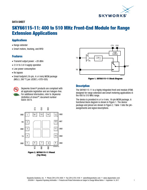
DATA SHEETSKY66115-11: 400 to 510 MHz Front-End Module for Range Extension ApplicationsApplications∙ Range extender∙ Smart meters, tracking, and RFIDFeatures∙ Transmit output power: +20 dBm ∙ 2.5 V to 3.6 V supply operation ∙ Low power consumption ∙ Rx bypass∙ Small footprint (16-pin, 4 x 4 mm) MCM package (MSL3, 260 ︒C per JEDEC J-STD-020)S kywork s Green TM product s are compliant with all applicable legi s lation and are halogen-free.For additional information, refer to Skyworks Definition of Green TM , document number SQ04–0074.GND RX GND TX GNDGND ANT GND GND GNDV C CG N DG N DC T XC S DV D D12345131211109678141516203309-002Figure 2. SKY66115-11 Pinout(Top View)RXTXFigure 1. SKY66115-11 Block DiagramDescriptionThe SKY66115-11 is a highly integrated front-end module (FEM)designed for range extension and smart metering applications in the 400 to 510 MHz range.The device is provided in a 4 x 4 mm, 16-pin MCM package. A functional block diagram is shown in Figure 1. The devicepackage and pinout are shown in Figure 2. Table 1 lists the pin-assignments and signal descriptions.DATA SHEET • SKY66115-11: 400 TO 510 MHz FRONT-END MODULE FOR RANGE EXTENSION APPLICATIONSTable 1. SKY66115-11 Signal DescriptionsPin Name Description Pin Name Description1 G ND G round 9G ND G round2 RX Receiveport 10 G ND G round3 G ND G round 11G ND G round4 TX Transmit port 12 ANT Antenna port5 G ND G round 13G ND G round6 VCC Positive power supply 14 VDD Positive power supply7 G ND G round 15 CSD Shutdown control signal8 G ND G round 16 CTX TX/RX control signalTechnical DescriptionThe SKY66115-11 consists of a complete T/R chain with a T/R switch contained in the module. The module has a shutdown mode to minimize power consumption.Transmit PathThe transmit path contains an amplifier optimized for saturated performance. The output is internally matched for optimum output power and efficiency into a 50 Ω load impedance. The output is passed through a harmonic filter before being fed through the switch. The input provides a good return loss into a 50 source impedance. Operation Mode ControlThe operating modes are controlled by the two digital pins (CSD and CTX, pins 15 and 16, respectively). The control logic truth table is provided in Table 8.Electrical and Mechanical SpecificationsThe absolute maximum ratings of the SKY66115-11 are provided in Table 2. Recommended operating conditions are specified in Table 3 and electrical specifications are provided in Tables 4 through 7. Table 8 shows the mode logic truth table.Typical performance characteristics are shown in Figures 3 through 8.Table 2. SKY66115-11 Absolute Maximum Ratings1Parameter Symbol Test Condition Minimum Maximum Units Supply voltage V CC 2.53.8V Control voltages V DD,V CSD,V CTX–0.2 V CC V RF input power, receive mode P IN_RX Rx mode at ANT +30 dBmRF input power, transmit mode P IN_TX Tx mode at TX 10 dBmVoltage standing wave ratio VSWR 10:1Operating temperature T A–40+85C Storage temperature T ST G–65+150C Transmit duty cycle 50 %1 Exposure to maximum rating conditions for extended periods may reduce device reliability. There is no damage to device with only one parameter set at the limit and all other parametersset at or below their nominal value. Exceeding any of the limits listed here may result in permanent damage to the device.ESD HANDLING: Although this device is designed to be as robust as possible, electrostatic discharge (ESD) can damage this device.This device must be protected at all times from ESD when handling or transporting. Static charges may easily producepotentials of several kilovolts on the human body or equipment, which can discharge without detection.Industry-standard ESD handling precautions should be used at all times.DATA SHEET • SKY66115-11: 400 TO 510 MHz FRONT-END MODULE FOR RANGE EXTENSION APPLICATIONSTable 3. SKY66115-11 Recommended Operating ConditionsParameter Symbol Min Typ Max Units Frequency1 f 400510MHz Supply voltages V CC,V DD 2.5 3.3 3.6 VControl voltages V CSD,V CTX 0 V DD VDigital input voltage (CSD and CTX):Logic 0 Logic 1 V LOWV HI G H2.80.45V DDVV1 Below 470 MHz, an external harmonic filter is required.Table 4. SKY66115-11 Electrical Specifications: DC Characteristics1(V CC =V DD = 3.3 V, T A= +25 °C, No RF Input Power, Unless Otherwise Noted)Parameter Symbol Test Condition Min Typ Max Units Rx current I CQ_RX_VDD RxMode 3 μA Tx quiescent current, VDD I CQ_TX_VDD TxMode 5 mA Tx quiescent current, VCC I CQ_TX_VCC TxMode 40 mA Tx operating current I OP_TX_VCC Tx Mode, P OUT = +20 dBm 67 mA Sleep current, VDD I DD_OFF SleepMode 3 μA Sleep current, VCC I CC_OFF SleepMode 0.04 1 μA Digital input current, logic 02I LOW SleepMode 0 μA Digital input current, logic 12I HI G H SleepMode 33 μA1 Performance is guaranteed only under the conditions listed in this table.2 Not production tested.Table 5. SKY66115-11 Electrical Specifications: Transmit Characteristics1(V CC =V DD = 3.3 V, T A= +25 °C, P OUT = +20 dBm, 470 to 510 MHz, Characteristic Impedance [Zo] = 50 Ω, Unless Otherwise Noted) Parameter Symbol Test Condition Min Typ Max Units Input power P IN_20dBm 4 dBm TX small signal gain |S21| P IN = –25 dBm 18 dB Input return loss |S11| 8 dB Output return loss |S22| 10 dB ANT to Rx isolation ISO_ANT_TO_RX35 dB 2nd to 10th harmonics22fo to 10fo P OUT = +20 dBm:< 1 G Hz > 1 G Hz –36–30dBmdBmRx to Tx transition time3t SWITCH 50%V CTX to 90% RF 0.6 μs Tx Power on time3t ON 50%V CSD to 90% RF 0.1 μs Tx Power off time3t OFF 50%V CSD to 10% RF 0.1 μs Non-harmonic spurious3P SPUR VSWR 6:1, all phases –42 dBm1 Performance is guaranteed only under the conditions listed in this table.2 2nd to 5th harmonics are production tested. 6th to 10th harmonics are characterized only.3 Not production tested.DATA SHEET • SKY66115-11: 400 TO 510 MHz FRONT-END MODULE FOR RANGE EXTENSION APPLICATIONSTable 6. SKY66115-11 Electrical Specifications: Receive Characteristics1(V CC =V DD = 3.3 V, T A= +25 °C, P IN = 0 dBm, 470 to 510 MHz, Characteristic Impedance [Zo] = 50 Ω, Unless Otherwise Noted) Parameter Symbol Test Condition Min Typ Max Units Insertion loss S21 0.7 dB Input return loss S11 18 dB Output return loss S22 18 dB Tx to Rx transition time2t SWITCH 50%V CTX to 90% RF 0.6 s 1 Performance is guaranteed only under the conditions listed in this table.2Not production tested.Table 7. SKY66115-11 Electrical Specifications: Control VoltagesParameter Symbol Min Typ Max Units Control voltage: 1Low High V LOWV HI G H2.80.45V DDVV1 VHI G H should always be lower than or equal to V DD.Table 8. SKY66115-11 Mode Logic Truth TableMode VCSD VCTXSleep mode1 0X Receive (Rx) mode X 0Transmit (Tx) mode 1 11 In the high state, CTX and CSD have an input current of 33 μA. The high state is not recommended for CTX whenthe device is in sleep mode.DATA SHEET • SKY66115-11: 400 TO 510 MHz FRONT-END MODULE FOR RANGE EXTENSION APPLICATIONSTypical Performance Characteristics (Note 1)(V CC = 3.3 V, T A = +25 ︒C, f = 470 to 510 MHz, All Unused Ports Terminated at 50 Ω, Unless Otherwise Noted)-80-75-70-65-60-55-50-45-40-35-30L e v e l (d B m )# Harmonic sFigure 3. Typical Harmonics Level at +20 dBm P OUTOutput Power (dBm)Figure 5. Typical Gain vs P OUT (V CC = 3.3 V)Figure 7. Typical Gain vs P OUT (V CC = 2.5 to 3.6 V)1I T O T A L (I C C + I D D , m A )P O U T (d B m )Input Power (dBm)203309-004Figure 4. Typical P OUT and I TOTAL Transfer CharacteristicsOutput Power (dBm)Figure 6. Typical I TOTAL vs P OUT (V CC = 3.3 V)Output Power (dBm)Figure 8. Typical PAE vs P OUT , CW (V CC = 2.5 to 3.6 V)DATA SHEET • SKY66115-11: 400 TO 510 MHz FRONT-END MODULE FOR RANGE EXTENSION APPLICATIONSEvaluation Board DescriptionThe SKY66115-11 Evaluation Board is used to test the performance of the SKY66115-11 front-end module. AnEvaluation Board schematic diagram is provided in Figure 9. An optional low-pass filter (LPF) can be incorporated on the ANT port to provide additional rejection of PA output harmonic levels and/or limit unwanted signals from entering the receive path. Table 9 identifies variations in components used for different EK# boards at their respective frequencies. The board layer detail is provided in Figure 10.PCB Recommendations:∙ Metal Layer 1 = RF traces + control lines. Core thickness between top RF layer and ground plane is critical. ∙ Metal Layer 2 = Solid ground plane. No traces routing. ∙ Metal Layer 3 and 4 = Control lines + VCC traces (no VCC plane).∙ Pour copper on each layer connected to the ground plane. Use VCC traces in a star distribution pattern. ∙ Always use four layers.S J3S J4s upply.Note: C3 is closest to DUT203309-009Figure 9. SKY66115-11 Evaluation Board SchematicTable 9. Components Used by Frequency Band and Corresponding EK BoardFrequency MHz C8 L1C1C2L2C9EK#470 to 510 DNI 0 Ω DNI DNI DNI 0 Ω EK1 420 to 440 3.9 pF 9.1 nH 2.7 pF 3.9 pF 15 nH 6.8 pF EK4 400 to 4203.9 pF10 nH4.0 pF6.0 pF15 nH8.0 pFEK5DATA SHEET • SKY66115-11: 400 TO 510 MHz FRONT-END MODULE FOR RANGE EXTENSION APPLICATIONS203309D-010Layer 1: Top – MetalLayer 2: GroundLayer 3: Ground + V CCLayer 4: S olid Ground PlaneFigure 10. SKY66115-11 Evaluation Board Layer Detail DiagramDATA SHEET • SKY66115-11: 400 TO 510 MHz FRONT-END MODULE FOR RANGE EXTENSION APPLICATIONSPackage DimensionsThe SKY66115-11 typical part marking is shown in Figure 11. The PCB layout footprint for the SKY66115-11 is shown in Figure 12. Package dimensions are shown in Figure 13, and tape and reel dimensions are provided in Figure 14. Package and Handling InformationSince the device package is sensitive to moisture absorption, it is baked and vacuum packed before shipping. Instructions on the shipping container label regarding exposure to moisture after the container seal is broken must be followed. Otherwise, problems related to moisture absorption may occur when the part is subjected to high temperature during solder assembly.The SKY66115-11 is rated to Moisture Sensitivity Level 3 (MSL3) at 250 C. It can be used for lead or lead-free soldering. For additional information, refer to Skyworks Application Note, PCB Design and SMT Assembly/Rework Guidelines for MCM-L Packages, document number 101752.Care must be taken when attaching this product, whether it is done manually or in a production solder reflow environment. Production quantities of this product are shipped in a standard tape and reel format.Pin 1S kywork sPart NumberLot C odeDate C ode:YY = C alendar YearWW = Work WeekCC = C ountry C ode Figure 11. SKY66115-11 Typical Part MarkingDATA SHEET • SKY66115-11: 400 TO 510 MHz FRONT-END MODULE FOR RANGE EXTENSION APPLICATIONSExpo s Expo s S tencil aperture s s older ma s Opening 6center opening Pin 1on 0.6Metallization (Top View)S tencil Aperture (Top View)S older Ma s k Opening(Top View)Notes:1. All measurements are in millimeters.2. Thermal vias should be resin filled and capped in accordance with IPC-4761 type VII vias. Recommended Cu thickness is 30 to 35 µm.203309-012Figure 12. SKY66115-11 PCB Layout FootprintDATA SHEET • SKY66115-11: 400 TO 510 MHz FRONT-END MODULE FOR RANGE EXTENSION APPLICATIONSPin 1IndicatorTop View0.S ide ViewTopS Ss k S older Ma s k Edge sEdge sEdge s(0.1)Detail APad S cale: 2X 3X Thi s Rotation 3X Rotated 90° C W 3X Rotated 180° 3X Rotated 90° CC WDetail BPad S cale: 2X 1X Thi s Rotation 1X Rotated 90° C W 1X Rotated 180° 1X Rotated 90° CC WDetail CPad (3 Place s )S cale: 2XDetail DPad S cale: 2XBottom ViewNotes:1. Dimensions and tolerances according to ASME Y14.5M-1994.2. All measurements are in millimeters.203309D-013Figure 13. SKY66115-11 Package DimensionsDATA SHEET • SKY66115-11: 400 TO 510 MHz FRONT-END MODULE FOR RANGE EXTENSION APPLICATIONSSkyworksSolutions,Inc.•Phone[781]376-3000•Fax[781]376-3100•*********************•203309H • Skyworks Proprietary Information • Products and Product Information are Subject to Change Without Notice • September 14, 201711203309-014Notes:1. Carrier tape material: black conductive polycarbonate or polystyrene.2. Cover tape material: transparent conductive PSA.3. Cover tape size: 9.3 mm width.4. Ten sprocket hole pitch cumulative tolerance: ±0.20 mm.5. Ao and Bo measured on plane 0.30 mm above the bottom of the pocket.6. Typical ESD surface resistivity is ≤1 x 10¹⁰ Ohms/square per EIA, JEDEC tape and reel specification.7. All measurements are in millimetersDetail BDetail AFigure 14. SKY66115-11 Tape and Reel DimensionsDATA SHEET • SKY66115-11: 400 TO 510 MHz FRONT-END MODULE FOR RANGE EXTENSION APPLICATIONSOrdering InformationModel Name Manufacturing Part Number Evaluation Board Part Number SKY66115-11: 470 to 510 MHz Front-End Module SKY66115-11 SKY66115-11EK1 (470 to 510 MHz) SKY66115-11: 420 to 440 MHz Front-End Module SKY66115-11 SKY66115-11EK4 (420 to 440 MHz) SKY66115-11: 400 to 420 MHz Front-End Module SKY66115-11 SKY66115-11EK5 (400 to 420 MHz)Copyright © 2014-2017 Skyworks Solutions, Inc. All Rights Reserved.Information in this document is provided in connection with Skyworks Solutions, Inc. (“Skyworks”) products or services. These materials, including the information contained herein, are provided by Skyworks as a service to its customers and may be used for informational purposes only by the customer. Skyworks assumes no responsibility for errors or omissions in these materials or the information contained herein. Skyworks may change its documentation, products, services, specifications or product descriptions at any time, without notice. Skyworks makes no commitment to update the materials or information and shall have no responsibility whatsoever for conflicts, incompatibilities, or other difficulties arising from any future changes.No license, whether express, implied, by estoppel or otherwise, is granted to any intellectual property rights by this document. Skyworks assumes no liability for any materials, products or information provided hereunder, including the sale, distribution, reproduction or use of Skyworks products, information or materials, except as may be provided in Skyworks Terms and Conditions of Sale.THE MATERIALS, PRODUCTS AND INFORMATION ARE PROVIDED “AS IS” WITHOUT WARRANTY OF ANY KIND, WHETHER EXPRESS, IMPLIED, STATUTORY, OR OTHERWISE, INCLUDIN G FITNESS FOR A PARTICULAR PURPOSE OR USE, MERCHANTABILITY, PERFORMANCE, QUALITY OR NON-INFRIN G EMENT OF ANY INTELLECTUAL PROPERTY RI G HT; ALL SUCH WARRANTIES ARE HEREBY EXPRESSLY DISCLAIMED. SKYWORKS DOES NOT WARRANT THE ACCURACY OR COMPLETENESS OF THE INFORMATION, TEXT, G RAPHICS OR OTHER ITEMS CONTAINED WITHIN THESE MATERIALS. SKYWORKS SHALL NOT BE LIABLE FOR ANY DAMA G ES, INCLUDIN G BUT NOT LIMITED TO ANY SPECIAL, INDIRECT, INCIDENTAL, STATUTORY, OR CONSEQUENTIAL DAMA G ES, INCLUDIN G WITHOUT LIMITATION, LOST REVENUES OR LOST PROFITS THAT MAY RESULT FROM THE USE OF THE MATERIALS OR INFORMATION, WHETHER OR NOT THE RECIPIENT OF MATERIALS HAS BEEN ADVISED OF THE POSSIBILITY OF SUCH DAMA G E.Skyworks products are not intended for use in medical, lifesaving or life-sustaining applications, or other equipment in which the failure of the Skyworks products could lead to personal injury, death, physical or environmental damage. Skyworks customers using or selling Skyworks products for use in such applications do so at their own risk and agree to fully indemnify Skyworks for any damages resulting from such improper use or sale.Customers are responsible for their products and applications using Skyworks products, which may deviate from published specifications as a result of design defects, errors, or operation of products outside of published parameters or design specifications. Customers should include design and operating safeguards to minimize these and other risks. Skyworks assumes no liability for applications assistance, customer product design, or damage to any equipment resulting from the use of Skyworks products outside of stated published specifications or parameters.Skyworks and the Skyworks symbol are trademarks or registered trademarks of Skyworks Solutions, Inc., in the United States and other countries. Third-party brands and names are for identification purposes only, and are the property of their respective owners. Additional information, including relevant terms and conditions, posted at , are incorporated by reference.SkyworksSolutions,Inc.•Phone[781]376-3000•Fax[781]376-3100•*********************•12 September 14, 2017 • Skyworks Proprietary Information • Products and Product Information are Subject to Change Without Notice • 203309HMouser ElectronicsAuthorized DistributorClick to View Pricing, Inventory, Delivery & Lifecycle Information:S kyworks:SKY66115-11SKY66115-11EK1SKY66115-11EK4。
AT070TN92 群创7寸屏datasheet
INNO L U X DISPLAY CORPORATIONLCD MODULESPECIFICATIONCustomer:Model Name: AT070TN92SPEC NO.: A070-92-TT-02Date: 2009/06/22Version: 02■Preliminary Specification□Final SpecificationFor Customer’s AcceptanceApproved by CommentApproved by Reviewed by Prepared byJoe Lin2009/06/23James Yu2009/06/22David Lee2009/06/22InnoLux copyright 2004All rights reserved,Copying forbidden.Record of RevisionVersion Revise Date Page ContentPre-Spec.01 2009/01/12 Initial Release02 2009/06/22 1 Add B/L & Panel power consumption.6 Add Vcom value.7Add current consumption.Update backlight driving condition.I NNO L U XContents1. General Specifications (1)2. Pin Assignment (2)3. Operation Specifications (5)3.1. Absolute Maximum Rating (5)3.1.1. Typical Operation Conditions (6)3.1.2. Current Consumption (7)3.1.3. Backlight Driving Conditions (7)3.2. Power Sequence (8)3.3. Timing Characteristics (9)3.3.1. AC Electrical Characteristics (9)3.3.2. Data Input Format (10)3.3.3. Timing (11)4. Optical Specifications (12)5. Reliability Test Items (16)6. General Precautions (17)6.1. Safety (17)6.2. Handling (17)6.3. Static Electricity (17)6.4. Storage (17)6.5. Cleaning (17)7. Mechanical Drawing (18)8. Package Drawing (19)8.1 Packaging Material Table (19)8.2 Packaging Quantity (19)8.3 Packaging Drawing (20)1. General SpecificationsNo. Item Specification Remark1 LCD size 7.0 inch(Diagonal)2 Driver element a-Si TFT active matrix3 Resolution 800 × 3(RGB) × 4804 Display mode Normally White, Transmissive5 Dot pitch 0.0642(W) × 0.1790(H) mm6 Active area 154.08(W) × 85.92(H) mm7 Module size 164.9(W) ×100.0(H) ×5.7(D) mm Note 18 Surface treatment Anti-Glare9 Color arrangement RGB-stripe10 Interface Digital11 Backlight power consumption 1.674W (Typ.)12 Panel power consumption 0.226W (Typ.)13 Weight (150g) (Typ.)Note 1: Refer to Mechanical Drawing.2. Pin AssignmentTFT LCD Panel Driving SectionFPC Connector is used for the module electronics interface. The recommended model is FH12A-50S-0.5SH manufactured by Hirose.Pin No. Symbol I/O Function Remark1 V LED+P Power for LED backlight (Anode)2 V LED+P Power for LED backlight (Anode)3 V LED-P Power for LED backlight (Cathode)4 V LED-P Power for LED backlight (Cathode)5 GND P Power ground6 V COM I Common voltage7 DV DD P Power for Digital Circuit8 MODE I DE/SYNC mode select Note 19 DE I Data Input Enable10 VS I Vertical Sync Input11 HS I Horizontal Sync Input12 B7 I Blue data(MSB)13 B6 I Blue data14 B5 I Blue data15 B4 I Blue data16 B3 I Blue data17 B2 I Blue data18 B1 I Blue data Note 219 B0 I Blue data(LSB) Note 220 G7 I Green data(MSB)21 G6 I Green data22 G5 I Green data23 G4 I Green data24 G3 I Green data26 G1 I Green data Note 227 G0 I Green data(LSB) Note 228 R7 I Red data(MSB)29 R6 I Red data30 R5 I Red data31 R4 I Red data32 R3 I Red data33 R2 I Red data34 R1 I Red data Note 235 R0 I Red data(LSB) Note 236 GND P Power Ground37 DCLK I Sample clock Note 338 GND P Power Ground39 L/R I Left / right selection Note 4,540 U/D I Up/down selection Note 4,541 V GH P Gate ON Voltage42 V GL P Gate OFF Voltage43 AV DD P Power for Analog Circuit44 RESET I Global reset pin. Note 645 NC - No connection46 V COM I Common Voltage47 DITHB I Dithering function Note 748 GND P Power Ground49 NC - No connection50 NC - No connectionI: input, O: output, P: PowerNote 1: DE/SYNC mode select. Normally pull high.When select DE mode, MODE=”1”, VS and HS must pull high.When select SYNC mode,MODE= ”0”, DE must be grounded.Note 2: When input 18 bits RGB data, the two low bits of R,G and B data must be grounded.Note 3:Data shall be latched at the falling edge of DCLK.Note 4: Selection of scanning modeSetting of scan control inputU/D L/RScanning directionGND DV DD Up to down, left to rightDV DD GND Down to up, right to leftGND GND Up to down, right to leftDV DD DV DD Down to up, left to rightNote 5: Definition of scanning direction.Refer to the figure as below:Note 6: Global reset pin. Active low to enter reset state. Suggest to connect with an RC reset circuit for stability. Normally pull high.Note 7: Dithering function enable control, normally pull high.When DITHB=”1”,Disable internal dithering function,When DITHB=”0”,Enable internal dithering function,RightLeftDownUp3. Operation Specifications3.1. Absolute Maximum Ratings(Note 1)ValuesItem SymbolMin. Max.Unit RemarkDV DD -0.3 5.0 VAV DD 6.5 13.5 VV GH -0.3 40.0 VV GL -20.0 0.3 V Power voltageV GH-V GL- 40.0 V Operation Temperature T OP -20 70 ℃Storage Temperature T ST-30 80 ℃LED Reverse Voltage V R- 1.2 VEach LEDNote 2 LED Forward Current I F- 25 mA Each LEDNote 1: The absolute maximum rating values of this product are not allowed to be exceeded at any times. Should a module be used with any of the absolute maximum ratingsexceeded, the characteristics of the module may not be recovered, or in an extremecase, the module may be permanently destroyed.Note 2: V R Conditions: Zener Diode 20mA3.1.1. Typical Operation Conditions( Note 1)ValuesUnit Remark Item SymbolMin. Typ. Max.DV DD 3.0 3.3 3.6 V Note 2AV DD 10.2 10.4 10.6 VPower voltageV GH 15.3 16.0 16.7 VV GL -7.7 -7.0 -6.3 VInput signal voltage V COM 3.8 4.0 4.2 VInput logic high voltage V IH 0.7 DV DD - DV DD VNote 3 Input logic low voltage V IL 0 - 0.3 DV DD VNote 1: Be sure to apply DV DD and V GL to the LCD first, and then apply V GH.Note 2: DV DD setting should match the signals output voltage (refer to Note 3) of customer’s system board.Note 3: DCLK,HS,VS,RESET,U/D, L/R,DE,R0~R7,G0~G7,B0~B7,MODE,DITHB.3.1.2. Current ConsumptionValuesItem SymbolMin. Typ. Max.Unit RemarkI GH - 0.2 1.0 mA V GH =16.0VI GL - 0.2 1.0 mA V GL = -7.0V IDV DD - 4.0 10 mA DV DD =3.3VCurrent for DriverIAV DD - 20 50 mA AV DD =10.4V3.1.3. Backlight Driving ConditionsValuesItem SymbolMin. Typ. Max.Unit Remark Voltage for LED backlight V L 8.7 9.3 9.9 V Note 1 Current for LED backlight I L 170 180 200 mALED life time - 20,000 - - Hr Note 2Note 1: The LED Supply Voltage is defined by the number of LED at Ta=25℃ andI L =180mA.Note 2: The “LED life time” is defined as the module brightness decrease to 50% original brightness at Ta=25℃ and I L =180mA. The LED lifetime could be decreased ifoperating I L is lager than 180mA.3.2. Power Sequencea. Power on:Note: Data include R0~R7, B0~B7, GO~G7, U/D, L/R, DCLK, HS,VS,DE.DV DD→VGL→VGH→Data→B/LB/L→Data→VGH→VGL→DV DD3.3. Timing Characteristics3.3.1. AC Electrical CharacteristicsValuesItem SymbolMin. Typ. Max.Unit Remark HS setup time T hst8 - - nsHS hold time T hhd 8 - - nsVS setup time T vst8 - - nsVS hold time T vhd8 - - nsData setup time T dsu8 - - nsData hole time T dhd8 - - nsDE setup time T esu 8 - - nsDE hole time T ehd8 - - nsDV DD Power On Slew rate T POR - - 20 ms From 0 to 90% DV DDRESET pulse width T Rst 1 - - ms DCLK cycle time T coh 20 - - ns DCLK pulse duty T cwh 40 50 60 %3.3.2. Data Input Format3.3.3. TimingValuesUnit Remark Item SymbolMin. Typ. Max.Horizontal Display Area thd- 800 - DCLKDCLK Frequency fclk26.4 33.3 46.8 MHzOne Horizontal Line th862 1056 1200 DCLKHS pulse width thpw 1 - 40 DCLKHS Blanking thb46 46 46 DCLKHS Front Porch thfp 16 210 354 DCLKValuesItem SymbolUnit RemarkMin. Typ. Max.Vertical Display Area tvd- 480 - THVS period time tv 510 525 650 THVS pulse width tvpw 1 - 20 THVS Blanking tvb23 23 23 THVS Front Porch tvfp 7 22 147 TH4. Optical SpecificationsValuesItem Symbol ConditionMin. Typ. Max.Unit RemarkθL Φ=180°(9 o’clock) 60 70 -θRΦ=0°(3 o’clock) 60 70 -θTΦ=90°(12 o’clock) 40 50 -Viewing angle(CR≥ 10)θBΦ=270°(6 o’clock) 60 70 -degree Note 1T ON - 10 20 msec Note 3 Response timeT OFF - 15 30 msec Note 3 Contrast ratio CR 400 500 - - Note 4W X 0.26 0.31 0.36 -Color chromaticityW Y 0.28 0.33 0.38 -Note 2Note 5Note 6 Luminance L 200 250 - cd/m² Note 6 LuminanceuniformityY UNormalθ=Φ=0°70 75 - % Note 7Test Conditions:1. DV DD=3.3V, I L=180mA (Backlight current), the ambient temperature is 25℃.2. The test systems refer to Note 2.Note 1: Definition of viewing angle rangeFig. 4-1 Definition of viewing angle Note 2: Definition of optical measurement system.The optical characteristics should be measured in dark room. After 30 minutesoperation, the optical properties are measured at the center point of the LCD screen. (Response time is measured by Photo detector TOPCON BM-7, other items are measured by BM-5A/Field of view: 1° /Height: 500mm.)Fig. 4-2 Optical measurement system setupNormal line θ=Φ=0°Photo detectorΦ=90°12 o’clock directionΦ=270°6 o’clock directionΦ=0°Φ=180°Active Area500mmLCMNormal line θ=Φ=0°Φ=90°12 o’clock directionΦ=270° 6 o’clock directionΦ=0°Φ=180°Active AreaθLθTθBθRLCMNote 3: Definition of Response timeThe response time is defined as the LCD optical switching time interval between“White” state and “Black” state. Rise time (T ON) is the time between photo detector output intensity changed from 90% to 10%. And fall time (T OFF) is the timebetween photo detector output intensity changed from 10% to 90%.Fig. 4-3 Definition of response timeNote 4: Definition of contrast ratiostateBlack""theonLCDwhenmeasuredLuminancestateWhite""theonLCDwhenmeasuredLuminance(CR)ratioContrast=Note 5: Definition of color chromaticity (CIE1931)Color coordinates measured at center point of LCD.Note 6: All input terminals LCD panel must be ground while measuring the center area of the panel.The LED driving condition is I L=180mA .90%10%0%Photodetectoroutput(Relativevalue)ONTWhite (TFT OFF) Black (TFT ON) White (TFT OFF)Note 7:Definition of Luminance UniformityActive area is divided into 9 measuring areas (Refer to Fig. 4-4 ).Every measuring point is placed at the center of each measuring area.maxminBB(Yu)UniformityLuminance=L-------Active area length W----- Active area widthWW/3W/3W/6L/3L/3L/6LFig. 4-4 Definition of measuring pointsB max: The measured maximum luminance of all measurement position.B min: The measured minimum luminance of all measurement position.5. Reliability Test Items(Note3)Item Test Conditions Remark High Temperature Storage Ta = 80℃240hrs Note 1,Note 4 Low Temperature Storage Ta = -30℃240hrs Note 1,Note 4 High Temperature Operation Ts = 70℃240hrs Note 2,Note 4 Low Temperature Operation Ta = -20℃240hrs Note 1,Note 4 Operate at High Temperatureand Humidity+60℃, 90%RH 240hrs Note 4Thermal Shock -30℃/30 min ~ +80℃/30 min for a total 100cycles, Start with cold temperature and endwith high temperature.Note 4Vibration Test Frequency range:10~55Hz Stroke:1.5mmSweep:10Hz~55Hz~10Hz2 hours for each direction of X. Y. Z.(6 hours for total)Mechanical Shock 100G 6ms,±X, ±Y, ±Z 3 times for each directionPackage Vibration Test Random Vibration :0.015G*G/Hz from 5-200HZ, -6dB/Octave from 200-500HZ2 hours for each direction of X. Y. Z.(6 hours for total)Package Drop Test Height:60 cm1 corner, 3 edges, 6 surfacesElectro Static Discharge ± 2KV, Human Body Mode, 100pF/1500ΩNote 1: Ta is the ambient temperature of samples.Note 2: Ts is the temperature of panel’s surface.Note 3: In the standard condition, there shall be no practical problem that may affect the display function. After the reliability test, the product only guarantees operation,but don’t guarantee all of the cosmetic specification.Note 4: Before cosmetic and function test, the product must have enough recovery time, at least 2 hours at room temperature.6. General Precautions6.1. SafetyLiquid crystal is poisonous. Do not put it in your mouth. If liquid crystal touches your skin or clothes, wash it off immediately by using soap and water.6.2. Handling1. The LCD panel is plate glass. Do not subject the panel to mechanical shock or toexcessive force on its surface.2. The polarizer attached to the display is easily damaged. Please handle it carefullyto avoid scratch or other damages.3. To avoid contamination on the display surface, do not touch the module surfacewith bare hands.4. Keep a space so that the LCD panels do not touch other components.5. Put cover board such as acrylic board on the surface of LCD panel to protect panelfrom damages.6. Transparent electrodes may be disconnected if you use the LCD panel underenvironmental conditions where the condensation of dew occurs.7. Do not leave module in direct sunlight to avoid malfunction of the ICs.6.3. Static Electricity1. Be sure to ground module before turning on power or operating module.2. Do not apply voltage which exceeds the absolute maximum rating value.6.4. Storage1. Store the module in a dark room where must keep at 25±10℃ and 65%RH or less.2. Do not store the module in surroundings containing organic solvent or corrosivegas.3. Store the module in an anti-electrostatic container or bag.6.5. Cleaning1. Do not wipe the polarizer with dry cloth. It might cause scratch.2. Only use a soft sloth with IPA to wipe the polarizer, other chemicals mightpermanent damage to the polarizer.7. Mechanical Drawing8. Package Drawing8.1. Packaging Material TableNo. ItemModel(Material)Dimensions(mm)UnitWeight(kg)Quantity Remark1 LCMModuleAT070TN92 164.9 × 100.0 × 5.7 (0.150) 50pcs2 Partition BC Corrugatedpaper512 × 349 × 226 1.466 1set3 CorrugatedPaperB Corrugatedpaper510 × 350 0.071 4pcs4 CorrugatedBarB Corrugatedpaper512 × 11 × 3 0.046 4pcs5 Dust-ProofBagPE 700 × 530 0.048 1pcs6 A/S Bag PE 180 × 133 × 0.2 0.002 50pcs7 Carton Corrugatedpaper530 × 355 × 255 1.100 1pcs8 Total weight (10.682 kg± 5%)8.1 Packaging QuantityTotal LCM quantity in Carton: no. of Partition 2 Rows × quantity per Row 25 = 508.2 Packaging Drawing。
射频PA sky77550 规格书datasheet
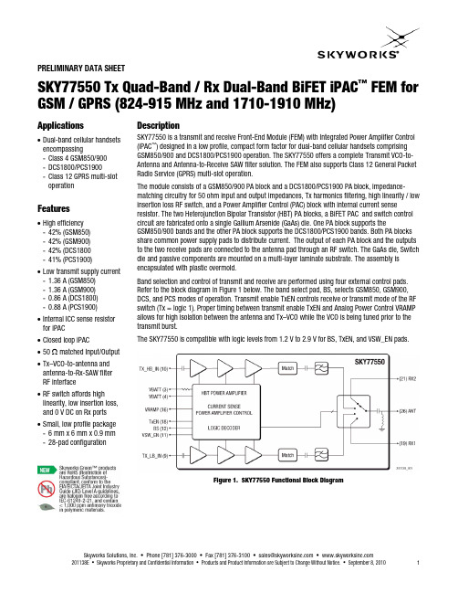
Skyworks Solutions, Inc. • Phone [781] 376-3000 • Fax [781] 376-3100 • sales@ •
2
September 8, 2010 • Skyworks Proprietary and Confidential Information • Products and Product Information are Subject to Change Without Notice. • 201138E
The module consists of a GSM850/900 PA block and a DCS1800/PCS1900 PA block, impedancematching circuitry for 50 ohm input and output impedances, Tx harmonics filtering, high linearity / low insertion loss RF switch, and a Power Amplifier Control (PAC) block with internal current sense resistor. The two Heterojunction Bipolar Transistor (HBT) PA blocks, a BiFET PAC and switch control circuit are fabricated onto a single Gallium Arsenide (GaAs) die. One PA block supports the GSM850/900 bands and the other PA block supports the DCS1800/PCS1900 bands. Both PA blocks share common power supply pads to distribute current. The output of each PA block and the outputs to the two receive pads are connected to the antenna pad through an RF switch. The GaAs die, Switch die and passive components are mounted on a multi-layer laminate substrate. The assembly is encapsulated with plastic overmold.
iw3616、3617、3630datasheet中文翻译(绝对真实)

产品特色大幅简化离线式LED驱动器设计●单级功率因数校正(PFC)与精确恒流(CC)输出相结合●输入/输出电容和变压器体积小●一次侧反馈控制,无需光耦电路,简化了电路设计●简化初级侧PWM调光接口●符合IEC61000-3-2标准高效节能和高兼容性●大幅提升效率,可达到85%以上●减少元件数量●总谐波失真<15%且PF>0.95●前沿、后沿和数字调光器●传感器和定时器精确稳定的性能●LED负载恒流精度不低于±5%●支持LED负载热插拔●1%-100%宽范围调光,调光无闪烁先进的保护及安全特性●通过自动重启动提供短路保护●开路故障检测模式●自动热关断重启动无论在PCB板上还是在封装上,都保证高压漏极引脚与其他所有信号引脚之间满足高压爬电要求应用●LED离线固态照明说明G7617 是一款的适用于LED调光控制的离线式两级交流/直流电源控制器,是适用于25W 输出功率的可调光LED 灯具的最优之选。
G7617符合电磁兼容性(EMC) IEC61000-3-2 标准,在120V AC或230V AC输入电压下其功率因数(PF) 可达到0.95 以上。
采用先进的数控技术来检测调光器的类型和相位,为调光器提供动态阻抗的同时可调节LED发光亮度,自动检测调光器类型和相位,从而实现了业内与模拟及数字调光器最广泛的兼容性。
G7617工作于准谐振工作模式,工作效率高,可工作于前沿后沿调光模式,也可工作于R 型、R-C型或R-L型调光控制模式。
G7617 符合热插拔LED 模块的固态照明行业标准Zhaga,同时还集成了调光功能的映射选项(位于白炽灯替代灯的NEMA SSL6 调光曲线内)。
G7617 系列有两个版本:针对120V AC输入应用进行优化的G7617-00 和针对230V AC 应用进行优化的G7617-01。
订购信息应用框图图1典型应用内部框图Vcc VinVcbVT CFGASU BisenseBdrvFdrvFisensePGNDAGND C O R E图2 内部框图引脚功能描述BV SENSE V IN BI SENSE B DRV CFG ASU V CCV CBV TFV SENSEFI SENSEF DRVAGNDPGND 图3. 引脚布局BV SENSE引脚:PFC电感电压反馈点,用于感知Boost电感的磁通状态。
新荷 Haven 显示 7.0 英寸 TFT 模块 (SPI) - 支持显示、触摸、音频说明书
NHD-7.0-800480FT-CSXN-T7.0” EVE2 TFT Module (SPI) – Supports: Display | Touch | Audio NHD- Newhaven Display7.0- 7.0” Diagonal800480- 800xRGBx480 PixelsFT- ModelC- On-board ControllerS- Sunlight ReadableX- TFTN- TN, Wide TemperatureT- Resistive Touch PanelNewhaven Display International, Inc.2661 Galvin Ct.Elgin IL, 60124Ph: 847-844-8795 Fax: 847-844-8796Functions and Features∙7.0” Sunl ight Readable EVE2 TFT Module w/ Resistive Touch∙On-board FTDI/Bridgetek FT812 Embedded Video Engine (EVE2)∙Supports Display, Touch, Audio∙SPI Interface (D-SPI/Q-SPI modes available)∙1MB of Internal Graphics RAM∙Built-in Scalable Fonts∙24-bit True Color, 800x480 Resolution (WVGA)∙Supports Portrait and Landscape modes∙Sunlight Readable (780 cd/m²)∙On-board ON Semiconductor FAN5333BSX High Efficiency LED Driver w/ PWM ∙4x Mounting Holes, enabling standard M3 or #6-32 screws∙Open-Source Hardware, Engineered in Elgin, IL (USA)[read caution below]CN2: FFC Connector - 20-Pin, 1.0mm pitch, Top-contact.NOTICE: It is not recommended to apply power to the board without a display connected. Doing so may result in a damaged LED driver circuit. Newhaven Display does not assume responsibility for failures due to this damage. Controller InformationThis EVE2 TFT Module is powered by the FTDI/Bridgetek FT812 Embedded Video Engine (EVE2).To view the full FT81x specification, please download it by accessing the link below:/Support/Documents/DataSheets/ICs/DS_FT81x.pdfThis product consists of the above TFT display assembled with a PCB which supports all the features of this module. For more details on the TFT display itself, please download the specification at:/specs/NHD-7.0-800480EF-ASXN-T.pdfArduino ApplicationIf using or prototyping this EVE2 TFT Module with the low-cost, widely popular Arduino platform we highly recommend using our Arduino shield, the NHD-FT81x-SHIELD. Not only does the NHD-FT81x-SHIELD provide seamless connectivity and direct software compatibility for the user, but it also comes with the following useful features on-board: ∙logic level shifters to allow the 5V Arduino to communicate with the 3.3V FT81x∙regulators to allow the Arduino to output more current to the EVE2 TFT Module∙audio filter/amplifier circuit to utilize the EVE2 TFT Module’s audio output signal∙microSD card slot, which allows expandable storage for data such as images, video, and audio to be stored. Please visit the NHD-FT81x-SHIELD product webpage for more info.Backlight Driver ConfigurationThe Backlight Driver Enable signal is connected to the FT81x backlight control pin. This signal is controlled by two registers: REG_PWM_HZ and REG_PWM_DUTY. REG_PWM_HZ specifies the PWM output frequency – the range available on the FT81x is 250 to 10000Hz, however the on-board backlight driver’s ma x PWM frequency is 1000Hz. Therefore, for proper use of the PWM function available on this module, the PWM frequency should not exceed 1000Hz. REG_PWM_DUTY specifies the duty cycle – the range is 0 to 128. A value of 0 turns the backlight completely off, while a value of 128 provides maximum backlight brightness.For the above register definitions, please refer to pages 80-81 of the official FT81x Series Programmers Guide:/Support/Documents/ProgramGuides/FT81X_Series_Programmer_Guide.pdfFT81x Block DiagramFT81x with EVE (Embedded Video Engine) technology simplifies the system architecture for advanced Human Machine Interfaces (HMIs) by providing support for display, touch, and audio as well as an object oriented architecture approach that extends from display creation to the rendering of the graphics.Serial Host InterfaceBy default the SPI slave operates in the SINGLE channel mode with MOSI as input from the master and MISO as output to the master. DUAL and QUAD channel modes can be configured through the SPI slave itself. To change the channel modes, write to register REG_SPI_WIDTH. Please refer to the table below:For more details on the FT81x SPI interface, please refer to pages 13-15 of the official FT81x Datasheet:/Support/Documents/DataSheets/ICs/DS_FT81x.pdfFor the REG_SPI_WIDTH register definition, please refer to page 87 of the official FT81x Series Programmers Guide: /Support/Documents/ProgramGuides/FT81X_Series_Programmer_Guide.pdfTFT Timing CharacteristicsShown below are the FT81x registers that control the TFT’s timing (clock and sync signals), along with the values recommended to use for this EVE2 TFT Module:Graphics EngineThe graphics engine executes the display list once for every horizontal line. It executes the primitive objects in the display list and constructs the display line buffer. The horizontal pixel content in the line buffer is updated if the object is visible at the horizontal line.Main features of the graphics engine are:∙The primitive objects supported by the graphics processor are: lines, points, rectangles, bitmaps (comprehensive set of formats), text display, plotting bar graph, edge strips, and line strips, etc.∙Operations such as stencil test, alpha blending and masking are useful for creating a rich set of effects such as shadows, transitions, reveals, fades and wipes.∙Anti-aliasing of the primitive objects (except bitmaps) gives a smoothing effect to the viewer.∙Bitmap transformations enable operations such as translate, scale and rotate.∙Display pixels are plotted with 1/16th pixel precision.∙Four levels of graphics states∙Tag buffer detectionThe graphics engine also supports customized built-in widgets and functionalities such as jpeg decode, screen saver, calibration etc. The graphics engine interprets commands from the MPU host via a 4 Kbyte FIFO in the FT81x memory at RAM_CMD. The MPU/MCU writes commands into the FIFO, and the graphics engine reads and executes the commands. The MPU/MCU updates the register REG_CMD_WRITE to indicate that there are new commands in the FIFO, and the graphics engine updates REG_CMD_READ after commands have been executed.Main features supported are:∙Drawing of widgets such as buttons, clock, keys, gauges, text displays, progress bars, sliders, toggle switches, dials, gradients, etc.∙JPEG and motion-JPEG decode∙Inflate functionality (zlib inflate is supported)∙Timed interrupt (generate an interrupt to the host processor after a specified number of milliseconds)∙In-built animated functionalities such as displaying logo, calibration, spinner, screen saver and sketch∙Snapshot feature to capture the current graphics displayFor a complete list of graphics engine display commands and widgets, please refer to Chapter 4 of the officialFT81x Series Programmers Guide:/Support/Documents/ProgramGuides/FT81X_Series_Programmer_Guide.pdfTouch-Screen EngineThe resistive touch-screen consists of a Touch-Screen Engine, ADC, Axis-switches, and ADC input multiplexer.The Touch-Screen Engine reads commands from the memory map register and generates the required control signals to the axis-switches and inputs mux and ADC. The ADC data are acquired, processed and updated in the respective register for the MPU/MCU to read.For more details on the FT812 Touch-Screen Engine, please refer to pages 32-33 of the official FT81x Datasheet:/Support/Documents/DataSheets/ICs/DS_FT81x.pdfAudio EngineThe FT81x provides mono audio output through a PWM output pin, AUDIO_L. It outputs two audio sources, the sound synthesizer and audio file playback.This pin is designed to be passed into a simple filter circuit and then passed to an amplifier for best results. Please refer to the example schematic in the Audio Filter and Amplifier Reference Circuit section on the next page.Sound SynthesizerA sound processor, AUDIO ENGINE, generates the sound effects from a small ROM library of waves table. To play a sound effect listed in Table 4.3, load the REG_SOUND register with a code value and write 1 to the REG_PLAY register. The REG_PLAY register reads 1 while the effect is playing and returns a ‘0’ when the effect ends. Some sound effects play continuously until interrupted or instructed to play the next sound effect. To interrupt an effect, write a new value to REG_SOUND and REG_PLAY registers; e.g. write 0 (Silence) to REG_SOUND and 1 to PEG_PLAY to stop the sound effect.The sound volume is controlled by register REG_VOL_SOUND. The 16-bit REG_SOUND register takes an 8-bit sound in the low byte. For some sounds, marked "pitch adjust" in the table below, the high 8 bits contain a MIDI note value. For these sounds, a note value of zero indicates middle C. For other sounds the high byte of REG_SOUND is ignored. Audio PlaybackThe FT81x can play back recorded sound through its audio output. To do this, load the original sound data into theFT81x’s RAM, and set r egisters to start the playback. The registers controlling audio playback are:REG_PLAYBACK_START: The start address of the audio data.REG_PLAYBACK_LENGTH: The length of the audio data, in bytes.REG_PLAYBACK_FREQ: The playback sampling frequency, in Hz.REG_PLAYBACK_FORMAT: The playback format, one of LINEAR SAMPLES, uLAW SAMPLES, orADPCM SAMPLES.REG_PLAYBACK_LOOP: If ‘0’, the sample is played once. If ‘1’, the sample is repeated indefinitely.REG_PLAYBACK_PLAY: A write to this location triggers the start of audio playback, regardless ofwriting ‘0’ or ‘1’. Read back ‘1’ when playback is ongoing, and ‘0’ wh enplayback finishes.REG_VOL_PB: Playback volume, 0-255.The mono audio formats supported are 8-bits PCM, 8-bits uLAW and 4-bits IMA-ADPCM. For ADPCM_SAMPLES, each sample is 4 bits, so two samples are packed per byte, the first sample is in bits 0-3 and the second is in bits 4-7.The current audio playback read pointer can be queried by reading the REG_PLAYBACK_READPTR. Using a large sample buffer, looping, and this read pointer, the host MPU/MCU can supply a continuous stream of audio.For more details on the FT81x Audio Engine, please refer to pages 30-32 of the official FT81x Datasheet:/Support/Documents/DataSheets/ICs/DS_FT81x.pdfAdditional Information/ResourcesFT81x Datasheet:FTDI/Bridgetek FT81x Embedded Video Engine (EVE2)/Support/Documents/DataSheets/ICs/DS_FT81x.pdfProgrammers Guide:FT81x Series Programmers Guide/Support/Documents/ProgramGuides/FT81X_Series_Programmer_Guide.pdfNHD GitHub Page:NHD EVE2 TFT Module Example Projectshttps:///NewhavenDisplay/EVE2-TFT-ModulesEVE2 Software Examples:FT81x Example Projects/Support/SoftwareExamples/FT800_Projects.htmFTDI/Bridgetek Utilities:Screen Designer/Support/Utilities.htm#ESD3Image Converters/Support/Utilities.htm#EVEImageConvertersAudio Converter/Support/Utilities.htm#EVEAudioConverterFont Converter/Support/Utilities.htm#EVEFontConverterFT80x to FT81x Migration Guide:FT80x to FT81x Migration Guide/Support/Documents/AppNotes/AN_390%20FT80x%20To%20FT81x%20Migration%20Guide.pdfNote 2: Conducted after 4 hours of storage at 25⁰C, 0%RH.Note 3:Test performed on product itself, not inside a container.Precautions for using LCDs/LCMsSee Precautions at /specs/precautions.pdfWarranty InformationSee Terms & Conditions at /index.php?main_page=terms。
天空工程解说说明书

Skyworks Solutions,Inc.•Phone [781]376-3000•Fax [781]376-3100••20027120071Chip On Board Mixer QuadsDATA SHEETFeaturesGHigh-volume automatic assemblyG For microwave MIC assembly and automated high-volume manufacturingG Mechanically rugged design G 100%DC testedG Three barrier heights for customized mixer performance G Available lead (Pb)-free,RoHS-compliant,andGreenDescriptionSkyworks ceramic Chip on Board (COB)mixer quads are designed for high-performance RF and microwave receiver applications.These devices utilize Skyworks advanced silicon beamless Schottky technology,combined with precision ceramic COB assembly techniques,to achieve a high degree of device reliability in commercial applications.CharacteristicValue Maximum current (I MAX )50mA Power dissipation (P D )CW 75mW/junction Storage temperature (T ST )-65°C to +175°C Operating temperature (T OP )-65°C to +150°CElectrostatic Discharge (ESD)Class 0Human Body Model (HBM)Absolute Maximum RatingsPerformance is guaranteed only under the conditions listed in the specifications table and is not guaranteed under the full range(s)described by the Absolute Maximum specifications.Exceeding any of the absolute maximum/minimum specifications may result in permanent damage to the device and will void the warranty.CAUTION:Although this device is designed to be as robust aspossible,ESD (Electrostatic Discharge)can damage this device.This device must be protected at all times from ESD.Static charges may easily produce poten-tials of several kilovolts on the human body or equipment,which can dischargewithout detection.Industry-standard ESD precautions must be employed at all times.Skyworks Green products are lead (Pb)-free,RoHS (Restriction of Hazardous Substances)-compliant,conform to the EIA/EICTA/JEITA Joint Industry Guide (JIG)Level A guidelines,and are free from antimony trioxide and brominated flame retardants.Skyworks Solutions,Inc.•Phone [781]376-3000•Fax [781]376-3100•*********************•2007200271DATA SHEET •CHIP-ON-BOARD MIXER QUADS2V F @1mA (∆) V F @ 1 mA 1C J @ 0 V (∆) C T @ 0 V 2R T @ 10 mAOutline Part Number Barrier(mV)(mV)(pF)(pF)(Ω)DrawingMin.Max.Max.Min.Max.Max.Max.Ring Quad (to 6 GHz)DMF3926-101Low 200260150.30.50.078101DME3927-101Medium 300400150.30.50.078101DMJ3928-101High 525625150.30.50.078101Crossover Ring Quad (to 6 GHz)DMF3926-100Low 200260150.30.50.078100DME3927-100Medium 300400150.30.50.078100DMJ3928-100High 525625150.30.50.078100Back-to-Back Crossover Quad (to 6 GHz)DMF3945-103Low 200260150.30.50.078103DME3946-103Medium 300400150.30.50.078103DMJ3947-103High525625150.30.50.078103V F @ 1 mA (∆) V F @ C J @ 0 V (∆) C T @ 0 V 2R T @ 10 mAV B @ 10 µAOutline Part Number Barrier(mV) 1 mA 1 (mV)(pF)(pF)(Ω)(V)DrawingMin.Max.Max.Min.Max.Max.Max.Min.Bridge Quad (to 6 GHz)DMF3929-102Low 200260150.30.50.0782102DME3930-102Medium 300400150.30.50.0783102DMJ3931-102High525625150.30.50.0784102Electrical Specifications at 25 °C1. Forward voltage difference between package electrodes.2. Capacitance difference between package electrodes.DATA SHEET • CHIP-ON-BOARD MIXER QUADSSkyworksSolutions,Inc.•Phone[781]376-3000•Fax[781]376-3100•*********************•3100, 101, 102103Shown For ClarityInk Dot 0.010 (0.25 mm) Dia. Min. 0.005 (0.13 mm)Max.± 0.002 (0.05 mm)Bottom side is free of metalization.The minimum specified area of the contact pads (0.017 x 0.022) shall be free of epoxy.Ceramic Substrate0.050(1.27 mm)Max.0.020 (0.51 mm) ± 0.002 (0.05 mm)0.130 (3.30 mm)± 0.003 (0.08 mm)0.140 (3.56 mm)± 0.003 (0.08 mm)Orientation SchematicDATA SHEET • CHIP-ON-BOARD MIXER QUADSCopyright © 2002, 2003, 2004, 2005, 2006, 2007, Skyworks Solutions, Inc. All Rights Reserved.Information in this document is provided in connection with Skyworks Solutions, Inc. (“Skyworks”) products or services. These materials, including the information contained herein, are provided by Skyworks as a service to its customers and may be used for informational purposes only by the customer. Skyworks assumes no responsibility for errors or omissions in these materials or the information contained herein. Skyworks may change its documentation, products, services, specifications or product descriptions at any time, without notice. Skyworks makes no commitment to update the materials or information and shall have no responsibility whatsoever for conflicts, incompatibilities, or other difficulties arising from any future changes.No license, whether express, implied, by estoppel or otherwise, is granted to any intellectual property rights by this document. Skyworks assumes no liability for any materials, products or information provided hereunder, including the sale, distribution, reproduction or use of Skyworks products, information or materials, except as may be provided in Skyworks Terms and Conditions of Sale.THE MATERIALS, PRODUCTS AND INFORMATION ARE PROVIDED “AS IS” WITHOUT WARRANTY OF ANY KIND, WHETHER EXPRESS, IMPLIED, STATUTORY, OR OTHERWISE, INCLUDING FITNESS FOR A PARTICULAR PURPOSE OR USE, MERCHANTABILITY, PERFORMANCE, QUALITY OR NON-INFRINGEMENT OF ANY INTELLECTUAL PROPERTY RIGHT; ALL SUCH WARRANTIES ARE HEREBY EXPRESSLY DISCLAIMED. SKYWORKS DOES NOT WARRANT THE ACCURACY OR COMPLETENESS OF THE INFORMATION, TEXT, GRAPHICS OR OTHER ITEMS CONTAINED WITHIN THESE MATERIALS. SKYWORKS SHALL NOT BE LIABLE FOR ANY DAMAGES, INCLUDING BUT NOT LIMITED TO ANY SPECIAL, INDIRECT, INCIDENTAL, STATUTORY, OR CONSEQUENTIAL DAMAGES, INCLUDING WITHOUT LIMITATION, LOST REVENUES OR LOST PROFITS THAT MAY RESULT FROM THE USE OF THE MATERIALS OR INFORMATION, WHETHER OR NOT THE RECIPIENT OF MATERIALS HAS BEEN ADVISED OF THE POSSIBILITY OF SUCH DAMAGE.Skyworks products are not intended for use in medical, lifesaving or life-sustaining applications, or other equipment in which the failure of the Skyworks products could lead to personal injury, death, physical or environmental damage. Skyworks customers using or selling Skyworks products for use in such applications do so at their own risk and agree to fully indemnify Skyworks for any damages resulting from such improper use or sale.Customers are responsible for their products and applications using Skyworks products, which may deviate from published specifications as a result of design defects, errors, or operation of products outside of published parameters or design specifications. Customers should include design and operating safeguards to minimize these and other risks. Skyworks assumes no liability for applications assistance, customer product design, or damage to any equipment resulting from the use of Skyworks products outside of stated published specifications or parameters. Skyworks, the Skyworks symbol, and “Breakthrough Simplicity” are trademarks or registered trademarks of Skyworks Solutions, Inc., in the United States and other countries. Third-party brands and names are for identification purposes only, and are the property of their respective owners. Additional information, including relevant terms and conditions, posted at , are incorporated by reference.SkyworksSolutions,Inc.•Phone[781]376-3000•Fax[781]376-3100•*********************•4。
Skyworks Inc. 天线耦合器数据表说明书
Phone[408]946-1968•Fax[408]946-1960•***************************•DATA SHEETDME, DMF, DMJ Series: Silicon Beam-Lead Schottky Mixer Diodes – Singles, Pairs, and Quads in Ceramic Hermetic PackagesApplications∙ Microwave integrated circuits ∙ Mixers ∙ DetectorsFeatures∙ Low 1/f noise∙ Low intermodulation distortion ∙ Hermetically sealed packages∙ Statistical process control wafer fabrication ∙ Packages rated MSL1, 260 ︒C per JEDEC J-STD-020)DescriptionThe Isolink silicon Schottky barrier mixer diodes are designed for applications through 20 GHz.Schottky barrier mixer diodes are made by the deposition of a suitable barrier metal on an epitaxial silicon substrate to form the junction. The process and choice of materials result in low series resistance with a narrow spread of capacitance values for close impedance control.A variety of forward voltages are available ranging from low values for low, or starved, local oscillator drive levels to high values for high drive, low distortion mixer applications. These Schottky barrier mixer diodes are available in a wide range of packages.Capacitance ranges and series resistances are comparable with the packaged devices that are available up to, and including, the Ka-band.Schottky barrier diodes are categorized by universal mixerapplications in six frequency ranges: S, C, X, Ku, K, and Ka bands as noted in Table 1. They may also be used as modulators and high-speed switches.The absolute maximum ratings of the DME, DMF, and DMJ series of Schottky mixer diodes are provided in Table 2. Electrical and physical specifications are provided in Tables 3 through 9. Typical performance characteristics are shown in Figures 1 through 3. Typical mixer circuits are shown in Figure 4. Package dimensions are provided in Figures 5 through 21.T a ble 1. Frequency TableFrequency BandFrequency (GHz) S 2 to 4 C 4 to 8 X 8.2 to 12.4 Ku 12.4 to 18.0 K 18.0 to 26.5 Ka26.5 to 40.0DATA SHEET • DME, DMF, DMJ SERIES SCHOTTKY MIXER DIODESTable 2. Absolute Maximum Ratings (Note 1)Pa ra meter SymbolMinimumTypica lMa ximumUnits Maximum current Imax 100 mAPower dissipation (continuous wave) Pd 75 mW/junctionStorage temperature T STG –65 +175︒C Operating temperature T A –65 +175︒CElectrostatic discharge:Human Body Model (HBM), Class 0 ESD< 250 VNote 1: Exposure to maximum rating conditions for extended periods may reduce device reliability. There is no damage to device with only one parameter set at the limit and all other parameters set at or below their nominal value. Exceeding any of the limits listed here may result in permanent damage to the device.CAUTION: Although these devices are designed to be as robust as possible, electrostatic discharge (ESD) can damage them. These devices must be protected at all times from ESD. Static charges may easily produce potentials of several kilovolts on thehuman body or equipment, which can discharge without detection. Industry-standard ESD precautions should be used at all times.DATA SHEET • DME, DMF, DMJ SERIES SCHOTTKY MIXER DIODESTable 3. Electrical Specifications: Beam-Lead Single N-Type Low, Medium, High Drive Schottky DiodesFrequencyBa nd Pa rtNumber Ba rrierV F @ 1.0 mA(mV)R s@ 5.0 mA(Ω)TotalCapacitance (CT) @ 0 V(pF)V B @ 10 uA(V) Minimum Ma ximum Ma ximum Ma ximum MinimumS, C DMF2820-220 Low 200 260 5 0.60 2 S, C DMF2820-250 Low 200 260 5 0.60 2 S, C DME2127-220 Medium 300 400 5 0.60 3 S, C DME2127-250 Medium 300 400 5 0.60 3 S, C DMJ2823-220 High 500 600 5 0.60 4 S, C DMJ2823-250 High 500 600 5 0.60 4 X DMF2821-220 Low 220 300 8 0.40 2 X DMF2821-250 Low 220 300 8 0.40 2 X DME2957-220 Medium 325 425 8 0.40 3 X DME2957-250 Medium 325 425 8 0.40 3 X DMJ2777-220 High 550 650 8 0.40 4X DMJ2777-250 High 550 650 8 0.40 4 Ku DMF2344-220 Low 260 330 13 0.25 2Ku DMF2344-230 Low 260 330 13 0.25 2Ku DMF2344-250 Low 260 330 13 0.25 2Ku DME2333-220 Medium 350 450 13 0.25 3Ku DME2333-230 Medium 350 450 13 0.25 3Ku DME2333-250 Medium 350 450 13 0.25 3Ku DMJ2824-220 High 500 680 13 0.25 4Ku DMJ2824-230 High 500 680 13 0.25 4Ku DMJ2824-250 High 500 680 13 0.25 4 K, Ka DMF2822-220 Low 270 350 18 0.25 2K, Ka DMF2822-230 Low 270 350 18 0.25 2K, Ka DME2458-220 Medium 375 550 18 0.2 3K, Ka DME2458-230 Medium 375 550 18 0.2 3K, Ka DMJ2825-220 High 600 700 18 0.2 4K, Ka DMJ2825-230 High 600 700 18 0.2 4DATA SHEET • DME, DMF, DMJ SERIES SCHOTTKY MIXER DIODESTable 4. Electrical Specifications: Beam-Lead Series Pair, N-Type Low, Medium, High Drive Schottky DiodesDATA SHEET • DME, DMF, DMJ SERIES SCHOTTKY MIXER DIODESTable 5. Electrical Specifications: Beam-Lead Common Cathode, N-Type Low, Medium, High Drive Schottky DiodesFrequencyBa nd Pa rtNumber Ba rrierV F @ 1.0 mA(mV)R s@ 5.0 mA(Ω)TotalCapacitance(CT) @ 0 V(pF)V B @ 10 uA(V) Minimum Ma ximum Ma ximum Ma ximum MinimumS, C DMF2182-223 Low 200 260 5 0.60 2S, C DMF2182-253 Low 200 260 5 0.60 2S, C DME2205-223 Medium 300 400 5 0.60 3S, C DME2205-253 Medium 300 400 5 0.60 3S, C DMJ2208-223 High 500 600 5 0.60 4S, C DMJ2208-253 High 500 600 5 0.60 4X DMF2183-223 Low 220 300 8 0.40 2 X DMF2183-253 Low 220 300 8 0.40 2 X DME2206-223 Medium 325 425 8 0.40 3 X DME2206-253 Medium 325 425 8 0.40 3 X DMJ2209-223 High 550 650 8 0.40 4 X DMJ2209-253 High 550 650 8 0.40 4 Ku DMF2184-223 Low 260 330 13 0.25 2 Ku DMF2184-253 Low 260 330 13 0.25 2 Ku DME2207-223 Medium 350 450 13 0.25 3 Ku DME2207-253 Medium 350 450 13 0.25 3 Ku DMJ2210-223 High 500 680 13 0.25 4 Ku DMJ2210-253 High 500 680 13 0.25 4 K, Ka DMF2834-223 Low 270 350 18 0.2 2K, Ka DME2864-223 Medium 375 550 18 0.2 3K, Ka DMJ2836-223 High 600 700 18 0.2 4DATA SHEET • DME, DMF, DMJ SERIES SCHOTTKY MIXER DIODESTable 6. Electrical Specifications: Beam-Lead Anti-Parallel, N-Type Low, Medium, High Drive Schottky DiodesDATA SHEET • DME, DMF, DMJ SERIES SCHOTTKY MIXER DIODES Table 7. Electrical Specifications: Beam-Lead Ring Quad, N-Type Low, Medium, High Drive Schottky DiodesDATA SHEET • DME, DMF, DMJ SERIES SCHOTTKY MIXER DIODESTable 8. Electrical Specifications: Beam-Lead Bridge Quad, N-Type Low, Medium, High Drive Schottky DiodesDATA SHEET • DME, DMF, DMJ SERIES SCHOTTKY MIXER DIODESTable 9. Electrical Specifications: Epoxy Packaged Octo Quad Ring, N-Type Low, Medium, High Drive Schottky DiodesTypical Performance Characteristics0.001120240360480600F o r w a r d C u r r e n t (m A )Forward Voltage (mV)0.0020.0050.010.020.050.10.20.51.02.05.010.0Figure 1. Typical Forward DC Characteristic Curves(Voltage vs Current)100Local Oscillator Driver (mW)200300400500600700ZIF (Ω)6789101112NF (dB)01.02.03.04.05.06.00.050.10.20.512510ZIFNFCC (mA)CCFigure 3. Typical X-Band Low Drive Mixer Diode RF Parameters vsLocal Oscillator Drive0.00100.4800.960 1.440 1.920 2.400Forward Voltage (mV)F o r w a r d C u r r e n t (m A )0.0020.0050.010.020.050.10.20.51.02.05.010.0Figure 2. Typical Forward DC Characteristic Curves(Voltage vs current)DATA SHEET • DME, DMF, DMJ SERIES SCHOTTKY MIXER DIODESS ingle Ended MixerS I G InputLO InputBalanced MixerS I G InputLO InputI G Input Double Balanced MixerFigure 4. Typical Mixer CircuitsFigure 5. -220 Package DimensionsY1187Figure 6. -221 Package DimensionsS chematic0.068 (1.73 mm)6 mm)6 mm).0.185 (4.70 mm)0.145 (3.68 mm)0.005 (0.13 mm)0.003 (0.08 mm)3 Plc s .0.042 (1.07 mm)0.028 (0.71 mm)0.070 (1.78 mm)Figure 7. -222 Package Dimensions-013 (223)S chematic 0.068 (1.73 mm)6 mm)6 mm).0.185 (4.70 mm)0.005 (0.13 mm)0.003 (0.08 mm)3 Plc s .0.042 (1.07 mm)0.028 (0.71 mm)0.070 (1.78 mm)Figure 8. -223 Package DimensionsS chematic40.042 (1.07 mm)0.028 (0.71 mm)(1.78mm)Figure 9. -224 Package DimensionsSchematic40.022 (0.56 mm)20.005 (0.13 mm)0.003 (0.08 mm)4 Plc s .0.028 (0.71 mm)0.070 (1.78 mm)S q.Figure 10. -225 Package DimensionsS chematic0.055 (1.40 mm)90 (2.29 mm)Min. 2 Plc s .0.013 (0.33 mm)0.017 (0.43 mm)2 Plc s .0.003 (0.08 mm)0.005 (0.13 mm)0.012 (0.30 mm)0.0306 mm) Max.Figure 11. -230 Package DimensionsS chematic21C 0.012 (0.30 mm)(0.76 mm)Figure 12. -232 Package Dimensions30.051 (1.30 mm)0.055 (1.40 mm)(0.76 mm)Max.4SchematicFigure 13. -234 Package DimensionsSchematic0.003 (0.08 mm)0.005 (0.13 mm)4 Plc s .0.055 (1.40 mm)6 mm)Max.0.008 (0.30 mm)4Figure 14. -235 Package DimensionsSchematic 0.018 (0.45 mm)0.122 (0.55 mm)2 Plc s .0 (2.28 mm)9 mm)2 Plc s .0.100 (2.54 mm)Max.0.003 (0.08 mm)0.005 (0.13 mm)Figure 15. -250 Package DimensionsS chematic0.022 (0.55 mm)0.018 (0.45 mm)0.022 (0.55 mm)2 Plc s .0.090 (2.28 mm)0.110 (2.79 mm)2 Plc s .0.100(2.54 mm)Dia.Max.Figure 16. -251 Package DimensionsS chematicC olored Dots0.021 (0.53 mm)0.018 (0.45 mm)0.022 (0.55 mm)3 Plc s.0.100Dia.0.050Figure 17. -252 Package Dimensions3S chematicCDenote s0.021 (0.33 mm)Max.3 Plc s.Figure 18. -253 Package DimensionsS chematicC Denote s C eramic Ba s e0.019 (0.46 mm)0.022 (0.56 mm)4 Plc s .0.018 (0.360.022 (0.562 Plc s .9 mm)s .0.100 (2.54 mm)0.012(0.30 mm)Max.Max.Figure 19. -254 Package Dimensions4S chematic0.022 (0.56 mm)0.003 (0.08 mm)0.005 (0.13 mm)Figure 20. -255 Package Dimensions2S chematic0.022 (0.56 mm)0.0506 mm) Max.0.012 (0.030 mm)Max.0.003 (0.08 mm)0.005 (0.13 mm)Figure 21. -257 Package DimensionsCopyright © 2014, 2017 Isolink, Inc. All Rights Reserved.Information in this document is provided in connection with Isolink, Inc. (“Isolink”), a wholly-owned subsidiary of Skyworks Solutions, Inc. These materials, including the information contained herein, are provided by Isolink as a service to its customers and may be used for informational purposes only by the customer. Isolink assumes no responsibility for errors or omissions in these materials or the information contained herein. Isolink may change its documentation, products, services, specifications or product descriptions at any time, without notice. Isolink makes no commitment to update the materials or information and shall have no responsibility whatsoever for conflicts, incompatibilities, or other difficulties arising from any future changes.No license, whether express, implied, by estoppel or otherwise, is granted to any intellectual property rights by this document. Isolink assumes no liability for any materials, products or information provided hereunder, including the sale, distribution, reproduction or use of Isolink products, information or materials, except as may be provided in Isolink Terms and Conditions of Sale.THE MATERIALS, PRODUCTS AND INFORMATION ARE PROVIDED “AS IS” WITHOUT WARRANTY OF ANY KIND, WHETHER EXPRESS, IMPLIED, STATUTORY, OR OTHERWISE, INCLUDING FITNESS FOR A PARTICULAR PURPOSE OR USE, MERCHANTABILITY, PERFORMANCE, QUALITY OR NON-INFRINGEMENT OF ANY INTELLECTUAL PROPERTY RIGHT; ALL SUCH WARRANTIES ARE HEREBY EXPRESSLY DISCLAIMED. ISOLINK DOES NOT WARRANT THE ACCURACY OR COMPLETENESS OF THE INFORMATION, TEXT, GRAPHICS OR OTHER ITEMS CONTAINED WITHIN THESE MATERIALS. ISOLINK SHALL NOT BE LIABLE FOR ANY DAMAGES, INCLUDING BUT NOT LIMITED TO ANY SPECIAL, INDIRECT, INCIDENTAL, STATUTORY, OR CONSEQUENTIAL DAMAGES, INCLUDING WITHOUT LIMITATION, LOST REVENUES OR LOST PROFITS THAT MAY RESULT FROM THE USE OF THE MATERIALS OR INFORMATION, WHETHER OR NOT THE RECIPIENT OF MATERIALS HAS BEEN ADVISED OF THE POSSIBILITY OF SUCH DAMAGE.Customers are responsible for their products and applications using Isolink products, which may deviate from published specifications as a result of design defects, errors, or operation of products outside of published parameters or design specifications. Customers should include design and operating safeguards to minimize these and other risks. Isolink assumes no liability for applications assistance, customer product design, or damage to any equipment resulting from the use of Isolink products outside of stated published specifications or parameters.Isolink is a trademark of Isolink Inc. in the United States and other countries. Skyworks and the Skyworks symbol are trademarks or registered trademarks of Skyworks Solutions, Inc., in the United States and other countries. Third-party brands and names are for identification purposes only, and are the property of their respective owners.。
Skyworks AAT1278 1.5A单光源闪光灯驱动器评估板数据表说明书
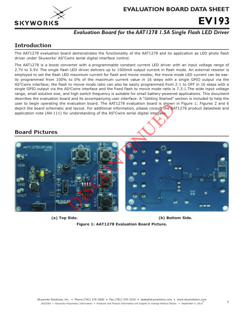
IntroductionThe AAT1278 evaluation board demonstrates the functionality of the AAT1278 and its application as LED photo flash driver under Skyworks' AS 2Cwire serial digital interface control.The AAT1278 is a boost converter with a programmable constant current LED driver with an input voltage range of 2.7V to 5.5V . The single flash LED driver delivers up to 1500mA output current in flash mode. An external resistor is employed to set the flash LED maximum current for flash and movie modes; the movie mode LED current can be eas-ily programmed from 100% to 0% of the maximum current value in 16 steps with a single GPIO output via the AS 2Cwire interface; the flash to movie mode ratio can also be easily programmed from 2:1 to OFF in 16 steps with a single GPIO output via the AS 2Cwire interface and the fixed flash to movie mode ratio is 7.3:1.The wide input voltage range, small solution size, and high switch frequency is suitable for small battery-powered applications. This document describes the evaluation board and its accompanying user interface. A “Getting Started” section is included to help the user to begin operating the evaluation board. The AAT1278 evaluation board is shown in Figure 1; Figures 2 and 6 depict the board schematic and layout. For additional information, please consult the AAT1278 product datasheet and application note (AN-111) for understanding of the AS 2Cwire serial digital interface.Board Pictures(a) Top Side. (b) Bottom Side.Figure 1: AAT1278 Evaluation Board Picture.D I S CO NT I NU EDBoard SchematicFigure 2: AAT1278 Evaluation Board Schematic.Getting StartedThe board has two terminals labeled VIN and GND for the input power supply connection. Jump the JP1 to connect the V IN power to microcontroller VDD and AAT1278 IN. Jump JP2 to connect the SW4 to AAT1278 FLINHIBIT pin for inhib-iting flash current. Jump the JP3 to set the microcontroller to generate AS 2C code signal for driving LED. After all jump-ers are in the correct positions, apply power between 2.7V and 5.5V to the V IN and GND terminals to power the AAT1278 (U1) and microcontroller (U2); the red LED (LED1) should illuminate when the microcontroller is powered. The green LED (LED2) should flicker when microcontroller sends the AS 2C digital signal to AAT1278.Table1 shows the jumps’ function, Figure 3 shows the connection of the AAT1278 board.D I S CO NT ITable 1: Jumpers’ Function DescriptionFigure 3: AAT1278 Evaluation Board Demonstration Connection.User Interface FunctionalityThe user interface is provided by four push buttons: MMC (SW1), FMM (SW2), FLEN (SW3) and FLINH (SW4). A sum-mary of operational modes for each button is outlined in Table 2.Definition of Each Control• MMC—Movie Mode Control (SW1): Sets movie mode current. Each switch closure will incrementally decrease the movie mode current stating at 100% to 0% (off) in 16 steps. Refer to the AAT1278 datasheet for detailed explanations of movie mode operation.• FMM—Flash/Movie Mode Current Ratio Control (SW2): Sets Flash/Movie Mode Current Ratio. Each switch closure will incrementally decrease the flash/movie mode current ratio stating at 2:1 to 0% (off) in 16 steps. Refer to the AAT1278 datasheet for detailed explanations of Flash to Maximum Movie Mode Current Ratio operation.• FLEN—Manual Flash Enable (SW3): Initiates a flash of maximum flash current.• FLINH—Inhibit Flash (SW4): Inhibit a flash current into default movie-mode current levelD I S CO NT I NU EDTable 2: User Interface Functionality.LED Drive Current Set-UpLED Drive CurrentThe AAT1278 can be set up to provide 1.5A maximum flash mode current. The maximum flash mode current is set by R1 and can be set to 107kΩ for a maximum flash LED drive current of 1.5A. In this AAT1278 manual’s application R1 is set to 133kΩ for 1.2A maximum flash current. Flash current can be calculated using Equation1 by change the value of R1. Refer to the AAT1278 datasheet to program a desired flash current, the default maximum Movie Mode Current can be calculated using Equation2 in this AAT1278 manual.162kΩ ∙ AR 1I FL =1200mA7.3I MOVIE MODE = == 164.4mA I FL (FL to MM Ratio)AS²Cwire Interface and ControlJP3 connects GPIO (U2) and AAT1278 (U1) AS 2Cwire interface EN/SET , AS 2Cwire interface data is programmed by the microcontroller U2 and its associated push button function switches SW1, SW2. The movie current can be programmed from 100% to 0% of the maximum movie mode current in 16 linear steps controlled by AS 2Cwire data signal as shown in Table 3.The flash to movie mode ratio may be varied from 2:1 to OFF in 16 linear steps controlled by AS 2Cwire data signal as shown in Table 4, the default ratio between the flash current level and maximum movie mode current level is 7.3:1.D I S CO NT I NU EDTable 3: Movie Mode (MM) Current Programming.Table 4: Flash/Movie Mode Current Ratio.Test WaveformMovie Mode WaveformFigure 4 shows the waveform under movie mode controlled by AS 2Cwire with data code 5.The I OUT rises to 100mA (63% of maximum movie mode current) as expected.Figure 4: Movie Mode Current Controlled by AS 2Cwire Data(Ch1: V OUT ; Ch2: EN/SET; Ch3: I IN ; Ch4: I OUT ).D I S CO NT I NU EDMaximum Flash Current WaveformFigure 5 shows the AAT1278 Flash Current waveform with a FLEN pulse. I OUT maintains 1.2A when the flash enable pulse is asserted.Figure 5: Flash Current Operation with FLEN Pulse(Ch1: V OUT ; Ch2: FLEN; Ch3: I IN ; Ch4: I OUT ).D I S CO NT I NU EDMaximum Movie Mode Current WaveformFigure 6 shows the AAT1278 Maximum Movie Mode Current waveform with a FLINH pulse, while FLEN is keeping high. I OUT maintains 164mA when the FLINH pulse is asserted.Figure 6: Complete Flash current operation waveform(Ch1: FLINH pulse; Ch2: FLEN; Ch4: I OUT ).D I S CO NT I NU EDPrinted Circuit Board(a) Top Layer. (b) Bottom Layer.Figure 6: AAT1278 Evaluation Board.AAT1278 EVAL Component ListingTable 5: AAT1278 Evaluation Board Bill of Materials.I NU EDCopyright © 2012 Skyworks Solutions, Inc. All Rights Reserved.Information in this document is provided in connection with Skyworks Solutions, Inc. (“Skyworks”) products or services. These materials, including the information contained herein, are provided by Skyworks as a service to its customers and may be used for informational purposes only by the customer . Skyworks assumes no responsibility for errors or omissions in these materials or the information contained herein. Sky-works may change its documentation, products, services, specifications or product descriptions at any time, without notice. Skyworks makes no commitment to update the materials or information and shall have no responsibility whatsoever for conflicts, incompatibilities, or other difficulties arising from any future changes.No license, whether express, implied, by estoppel or otherwise, is granted to any intellectual property rights by this document. Skyworks assumes no liability for any materials, products or information provided here-under , including the sale, distribution, reproduction or use of Skyworks products, information or materials, except as may be provided in Skyworks Terms and Conditions of Sale.THE MATERIALS, PRODUCTS AND INFORMATION ARE PROVIDED “AS IS” WITHOUT WARRANTY OF ANY KIND, WHETHER EXPRESS, IMPLIED, STATUTORY , OR OTHERWISE, INCLUDING FITNESS FOR A PARTICULAR PURPOSE OR USE, MERCHANTABILITY , PERFORMANCE, QUALITY OR NON-INFRINGEMENT OF ANY INTELLECTUAL PROPERTY RIGHT; ALL SUCH WARRANTIES ARE HEREBY EXPRESSLY DISCLAIMED. SKYWORKS DOES NOT WARRANT THE ACCURACY OR COMPLETENESS OF THE INFORMATION, TEXT , GRAPHICS OR OTHER ITEMS CONTAINED WITHIN THESE MATERIALS. SKYWORKS SHALL NOT BE LIABLE FOR ANY DAMAGES, IN-CLUDING BUT NOT LIMITED TO ANY SPECIAL, INDIRECT , INCIDENTAL, STATUTORY , OR CONSEQUENTIAL DAMAGES, INCLUDING WITHOUT LIMITATION, LOST REVENUES OR LOST PROFITS THAT MAY RESULT FROM THE USE OF THE MATERIALS OR INFORMATION, WHETHER OR NOT THE RECIPIENT OF MATERIALS HAS BEEN ADVISED OF THE POSSIBILITY OF SUCH DAMAGE.Skyworks products are not intended for use in medical, lifesaving or life-sustaining applications, or other equipment in which the failure of the Skyworks products could lead to personal injury, death, physical or en-vironmental damage. Skyworks customers using or selling Skyworks products for use in such applications do so at their own risk and agree to fully indemnify Skyworks for any damages resulting from such improper use or sale.Customers are responsible for their products and applications using Skyworks products, which may deviate from published specifications as a result of design defects, errors, or operation of products outside of pub-lished parameters or design specifications. Customers should include design and operating safeguards to minimize these and other risks. Skyworks assumes no liability for applications assistance, customer product design, or damage to any equipment resulting from the use of Skyworks products outside of stated published specifications or parameters.Skyworks, the Skyworks symbol, and “Breakthrough Simplicity” are trademarks or registered trademarks of Skyworks Solutions, Inc., in the United States and other countries. Third-party brands and names are for identification purposes only, and are the property of their respective owners. Additional information, including relevant terms and conditions, posted at , are incorporated by reference.D I S CO NT I NU ED。
Skyworks Solutions SE5003L 5 GHz WLAN Power Amplif
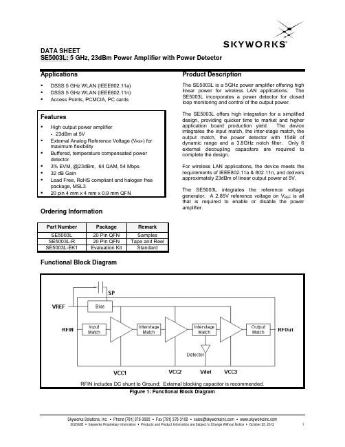
DATA SHEETSE5003L: 5 GHz, 23dBm Power Amplifier with Power Detector ▪ DSSS 5 GHz WLAN (IEEE802.11a) ▪ DSSS 5 GHz WLAN (IEEE802.11n) ▪ Access Points, PCMCIA, PC cardsFeatures▪ High output power amplifier - 23dBm at 5V▪ External Analog Reference Voltage (V REF ) for maximum flexibility▪ Buffered, temperature compensated power detector▪ 3% EVM, @23dBm, 64 QAM, 54 Mbps ▪ 32 dB Gain▪ Lead Free, RoHS compliant and halogen free package, MSL3▪20 pin 4 mm x 4 mm x 0.9 mm QFNOrdering InformationThe SE5003L is a 5GHz power amplifier offering high linear power for wireless LAN applications. The SE5003L incorporates a power detector for closed loop monitoring and control of the output power.The SE5003L offers high integration for a simplified design, providing quicker time to market and higher application board production yield. The device integrates the input match, the inter-stage match, the output match, the power detector with 15dB of dynamic range and a 3.8GHz notch filter. Only 6 external decoupling capacitors are required to complete the design.For wireless LAN applications, the device meets the requirements of IEEE802.11a & 802.11n, and delivers approximately 23dBm of linear output power at 5V.The SE5003L integrates the reference voltage generator. A 2.85V reference voltage on V REF is all that is required to enable or disable the power amplifier.Functional Block DiagramRFIN includes DC shunt to Ground; External blocking capacitor is recommended.Figure 1: Functional Block DiagramDATA SHEETSE5003L: 5 GHz, 23dBm Power Amplifier with Power DetectorFigure 2: SE5003L Pin Out (Top View Through Package)Pin Out DescriptionDATA SHEETSE5003L: 5 GHz, 23dBm Power Amplifier with Power DetectorThese are stress ratings only. Exposure to stresses beyond these maximum ratings for a long period of time may cause permanent damage to, or affect the reliability of the device. Avoid operating the device outside the recommended operating conditions defined below. This device is ESD sensitive. Handling and assembly of this device should be at ESD protected workstations.Recommended Operating ConditionsDC Electrical CharacteristicsConditions: V CC= 5.0V, V REF = 2.85 V, T A = 25 °C, as measured on Skyworks’ SE5003L-EK1 evaluation board,DATA SHEETSE5003L: 5 GHz, 23dBm Power Amplifier with Power Detector802.11a AC Electrical CharacteristicsConditions: V CC = 5.0 V, V REF = 2.85 V, f = 5.4 GHz, T A = 25 °C, as measured on Skyworks’ SE5003L-EK1DATA SHEETSE5003L: 5 GHz, 23dBm Power Amplifier with Power DetectorPower DetectorConditions: V CC = 5.0 V, V REF = 2.85 V, f = 5.4 GHz, T A = 25 °C, as measured on Skyworks’ SE5003L-EK1Figure 3: SE5003L Power Detector Characteristic over FrequencyDATA SHEETSE5003L: 5 GHz, 23dBm Power Amplifier with Power Detector Package DiagramFigure 4: SE5003L Package InformationDATA SHEETSE5003L: 5 GHz, 23dBm Power Amplifier with Power DetectorFigure 5: SE5003L Recommended Land PatternPackage Handling InformationBecause of its sensitivity to moisture absorption, instructions on the shipping container label must be followed regarding exposure to moisture after the container seal is broken, otherwise, problems related to moisture absorption may occur when the part is subjected to high temperature during solder assembly. The SE5003L is capable of withstanding a Pb free solder reflow. Care must be taken when attaching this product, whether it is done manually or in a production solder reflow environment. If the part is manually attached, precaution should be taken to insure that the device is not subjected to temperatures above its rated peak temperature for an extended period of time. For details on both attachment techniques, precautions, and handling procedures recommended, please refer to:▪“Quad Flat No-Lead Module Solder Reflow & Rework Information”, Document Number QAD-00045▪“Handling, Packing, Shipping and Use of Moisture Sensitive QFN”, Document Number QAD-00044Caution! Class 1B ESD sensitive deviceDATA SHEETSE5003L: 5 GHz, 23dBm Power Amplifier with Power DetectorFigure 6: SE5003L Branding InformationTape and Reel InformationFigure 7: SE5003L-R Tape and Reel InformationDATA SHEETSE5003L: 5 GHz, 23dBm Power Amplifier with Power DetectorCopyright © 2012 Skyworks Solutions, Inc. All Rights Reserved.Information in this document is provided in connection with Skyworks Solutions, Inc. (“Skyworks”) products or services. These materials, including the information contained herein, are provided by Skyworks as a service to its customers and may be used for informational purposes only by the customer. Skyworks assumes no responsibility for errors or omissions in these materials or the information contained herein. Skyworks may change its documentation, products, services, specifications or product descriptions at any time, without notice. Skyworks makes no commitment to update the materials or information and shall have no responsibility whatsoever for conflicts, incompatibilities, or other difficulties arising from any future changes.No license, whether express, implied, by estoppel or otherwise, is granted to any intellectual property rights by this document. Skyworks assumes no liability for any materials, products or information provided hereunder, including the sale, distribution, reproduction or use of Skyworks products, information or materials, except as may be provided in Skyworks Terms and Conditions of Sale.THE MATERIALS, PRODUCTS AND INFORMATION ARE PROVIDED “AS IS” WITHOUT WARRANTY OF ANY KIND, WHETHER EXPRESS, IMPLIED, STATUTORY, OR OTHERWISE, INCLUDING FITNESS FOR A PARTICULAR PURPOSE OR USE, MERCHANTABILITY, PERFORMANCE, QUALITY OR NON-INFRINGEMENT OF ANY INTELLECTUAL PROPERTY RIGHT; ALL SUCH WARRANTIES ARE HEREBY EXPRESSLY DISCLAIMED. SKYWORKS DOES NOT WARRANT THE ACCURACY OR COMPLETENESS OF THE INFORMATION, TEXT, GRAPHICS OR OTHER ITEMS CONTAINED WITHIN THESE MATERIALS. SKYWORKS SHALL NOT BE LIABLE FOR ANY DAMAGES, INCLUDING BUT NOT LIMITED TO ANY SPECIAL, INDIRECT, INCIDENTAL, STATUTORY, OR CONSEQUENTIAL DAMAGES, INCLUDING WITHOUT LIMITATION, LOST REVENUES OR LOST PROFITS THAT MAY RESULT FROM THE USE OF THE MATERIALS OR INFORMATION, WHETHER OR NOT THE RECIPIENT OF MATERIALS HAS BEEN ADVISED OF THE POSSIBILITY OF SUCH DAMAGE.Skyworks products are not intended for use in medical, lifesaving or life-sustaining applications, or other equipment in which the failure of the Skyworks products could lead to personal injury, death, physical or environmental damage. Skyworks customers using or selling Skyworks products for use in such applications do so at their own risk and agree to fully indemnify Skyworks for any damages resulting from such improper use or sale.Customers are responsible for their products and applications using Skyworks products, which may deviate from published specifications as a result of design defects, errors, or operation of products outside of published parameters or design specifications. Customers should include design and operating safeguards to minimize these and other risks. Skyworks assumes no liability for applications assistance, customer product design, or damage to any equipment resulting from the use of Skyworks products outside of stated published specifications or parameters.Skyworks, the Skyworks symbol, and “Breakthrough Simplicity” are trademarks or registered trademarks of Skyworks Solutions, Inc., in the United States and other countries. Third-party brands and names are for identification purposes only, and are the property of their respective owners. Additional information, including relevant terms and conditions, posted at , are incorporated by reference.。
SKY72301-22;中文规格书,Datasheet资料
DATA SHEETSKY72301-22: Spur-Free, 1.0 GHz Dual Fractional-N Frequency SynthesizerApplicationsx General purpose RF systemsx Low bit rate wireless telemetryx Instrumentationx Specialized Mobile Radios (SMRs) and Private Mobile Radios(PMRs)Featuresx Spur-free operationx1.0 GHz maximum operating frequencyx500 MHz maximum auxiliary synthesizerx Ultra-small step size, 100 Hz or lessx High internal reference frequency enables large loop bandwidthimplementationsx Very fast switching speed (e.g., below 100 P s)x Phase noise to –96 dBc/Hz inside the loop filter bandwidth@ 950 MHzx Software programmable power-down modesx High-speed serial interface up to 100 Mbpsx Three-wire programmingx Programmable division ratios on reference frequencyx Phase detectors with programmable gain provide aprogrammable loop bandwidthx Frequency power steering further enhances rapid acquistiontimex On-chip crystal oscillatorx Frequency adjust for temperature compensationx Direct digital modulationx3 V operationSkyworks offers lead (Pb)-free, RoHS (Restriction ofHazardous Substances) compliant packaging.x5 V output to loop filterx EP-TSSOP (28-pin, 9.7 x 6.4 x 1.1 mm) package (MSL3, 260 q Cper JEDEC J-STD-020)DescriptionSkyworks SKY72301-22 direct digital modulation fractional-Nfrequency synthesizer provides ultra-fine frequency resolution,fast switching speed, and low phase-noise performance. Thissynthesizer is a key building block for high-performance radiosystem designs that require low power and fine step size.The ultra-fine step size of less than 100 Hz allows this synthesizerto be used in very narrowband wireless applications. With propertemperature sensing or through control channels, thesynthesizer’s fine step size can compensate for crystal oscillatoror Intermediate Frequency (IF) filter drift. As a result, crystaloscillators or crystals can replace temperature- compensated orovenized crystal oscillators, reducing parts count and associatedcomponent cost. The device’s fine step size can also be used forDoppler shift corrections.The SKY72301-22 has a phase noise floor of –95 dBc/Hz up to1.0 GHz operation as measured inside the loop bandwidth. This ispermitted by the on-chip low noise dividers and low divide ratiosprovided by the device’s high fractionality.Reference crystals or oscillators up to 50 MHz can be used withthe SKY72301-22. The crystal frequency is divided down byindependent programmable divider ratios of 1 to 32 for the mainand auxiliary synthesizers. The phase detectors can operate at amaximum speed of 25 MHz, which allows better phase noise dueto the lower division value. With a high reference frequency, theloop bandwidths can also be increased. Larger loop bandwidthsimprove the settling times and reduce in-band phase noise.Therefore, typical switching times of less than 100 P s can beachieved. The lower in-band phase noise also permits the use oflower cost Voltage Controlled Oscillators (VCOs) in customerapplications.The SKY72301-22 has a frequency power steering circuit thathelps the loop filter steer the VCO when the frequency is too fastor too slow, further enhancing acquisition time.DATA SHEET • SKY72301-22 FREQUENCY SYNTHESIZERThe unit operates with a three-wire, high-speed serial interface. A combination of a large bandwidth, fine resolution, and the three-wire, high-speed serial interface allows for a direct frequency modulation of the VCO. This supports any continuous phase, constant envelope modulation scheme such as Frequency Modulation (FM), Frequency Shift Keying (FSK), Minimum Shift Keying (MSK), or Gaussian Minimum Shift Keying (GMSK).The capability to support such modulation schemes eliminates the need for In-Phase and Quadrature (I/Q) Digital-To-AnalogConverters (DACs), quadrature upconverters, and IF filters from the transmitter portion of the radio system.Figure 1 shows a functional block diagram for the SKY72301-22. The device package and pinout for the 28-pin Exposed Pad ThinShrink Small Outline Package (EP-TSSOP) are shown in Figure 2.C1447Figure 1. SKY72301-22 Functional Block DiagramC141212345678910111213142827262524232221201918171615Clock Mod_in Mux_out VSUBdigital GNDcml VCCcml_main Fvco_main Fvco_main LD/PSmain VCCcp_main CPout_main GNDcp_main Xtalacgnd/OSCXtalin/OSCCS Data VCCdigital GNDdigital VCCcml_aux VCCvco_aux Fvco_aux GNDcp_aux CPout_aux VCCcp_aux LD/PSaux GNDxtal VCCxtal Xtalout/NCFigure 2. SKY72301-22 Pinout, 28-Pin EP-TSSOP(Top View)DATA SHEET • SKY72301-22 FREQUENCY SYNTHESIZERTechnical DescriptionThe SKY72301-22 is a fractional-N frequency synthesizer using a '6 modulation technique. The fractional-N implementation provides low in-band noise by having a low division ratio and fast frequency settling time. In addition, the SKY72301-22 provides arbitrarily fine frequency resolution with a digital word, so that the frequency synthesizer can be used to compensate for crystal frequency drift in the RF transceiver.Serial InterfaceThe serial interface is a versatile three-wire interface consisting of three pins: Clock (serial clock), Data (serial input), and CS (chip select). It enables the SKY72301-22 to operate in a system where one or multiple masters and slaves are present. To perform a loopback test at start-up and to check the integrity of the board and processor, the serial data is fed back to the master device (e.g., a microcontroller or microprocessor unit) through a programmable multiplexer. This facilitates hardware and software debugging.RegistersThere are ten 16-bit registers in the SKY72301-22. For more information, see the Register Descriptions section of this document.Main and Auxiliary '6 ModulatorsThe fractionality of the SKY72301-22 is accomplished by the use of a proprietary, configurable 10-bit or 18-bit '6 modulator for the main synthesizer and 10-bit '6 modulator for the auxiliary synthesizer.Main and Auxiliary Fractional UnitsThe SKY72301-22 provides fractionality through the use of main and auxiliary '6 modulators. The output from the modulators is combined with the main and auxiliary divider ratios through their respective fractional units.VCO PrescalersThe VCO prescalers provide low-noise signal conditioning of the VCO signals. They translate from an off-chip, single-ended or differential signal to an on-chip differential Current Mode Logic (CML) signal. The SKY72301-22 has independent main and auxiliary VCO prescalers.Main and Auxiliary VCO DividersThe SKY72301-22 provides programmable dividers that control the CML prescalers and supply the required signals to the charge pump phase detectors. Programmable divide ratios ranging from 38 to 537 are possible in fractional-N mode and from 32 to 543 in integer-N mode.Reference Frequency OscillatorThe SKY72301-22 has a self-contained, low-noise crystal oscillator. This crystal oscillator is followed by the clock generation circuitry that generates the required clock for the programmable reference frequency dividers.Reference Frequency DividersThe crystal oscillator signal can be divided by a ratio of 1 to 32 to create the reference frequencies for the phase detectors. The SKY72301-22 has both a main and an auxiliary frequency synthesizer, and provides independently configurable dividers of the crystal oscillator frequency for both the main and auxiliary phase detectors. The divide ratios are programmed by the Reference Frequency Dividers Register.NOTE: The divided crystal oscillator frequencies (which are the internal reference frequencies), Fref_main and Fref_aux,are referred to as the reference frequencies throughoutthis document.Phase Detectors and Charge PumpsThe SKY72301-22 uses a separate charge pump phase detector for each synthesizer which provides a programmable gain, Kd, from 31.25 to 1000 P A/2S radians in 32 steps programmed using the Phase Detector/Charge Pumps Control Register. Frequency SteeringWhen programmed for frequency power steering, the SKY72301-22 has a circuit that helps the loop filter steer the VCO using the LD/PSmain signal (pin 9). In this configuration, the LD/PSmain signal can provide a more rapid acquisition.When programmed for lock detection, internal frequency steering is implemented and provides frequency acquisition times comparable to conventional phase/frequency detectors.Lock DetectionWhen programmed for lock detection, the SKY72301-22 provides an active low, pulsing open collector output using the LD/PSmain signal (pin 9) to indicate the out-of-lock condition. When locked, the LD/PSmain signal is tri-stated (high impedance).Power DownThe SKY72301-22 supports a number of power-down modes through the serial interface. For more information, see the Register Descriptions section of this document.DATA SHEET • SKY72301-22 FREQUENCY SYNTHESIZERSerial Interface OperationRegister ProgrammingThe serial interface consists of three signals: Clock (pin 1), Data (pin 27) and CS (pin 28). The Clock signal controls data on the two temporary register on the rising edge of Clock. The CS line allows individual selection transfers that synchronize and sample the information of slave devices on the same bus.Register programming equations, described in this section, use the following variables and constants: N fractionalDesired VCO division ratio in fractional-N applications. This is a real number and can be interpreted as the reference frequency (F ref ) multiplying factor such that the resulting frequency is equal to the desired VCO frequency.Figure 3 functionally depicts how a serial transfer takes place. A serial transfer is initiated when a microcontroller ormicroprocessor forces the CS line to a low state. This is followed immediately by an address/data stream sent to the Data pin that coincides with the rising edges of the clock presented on the Clock line.N integerDesired VCO division ratio in integer-N applications. This number is an integer and can be interpreted as the reference frequency (F ref ) multiplying factor so that the resulting frequency is equal to the desired VCO frequency.Each rising edge of the Clock signal shifts in one bit of data on the Data line into a shift register. At the same time, one bit of data is shifted out of the Mux_out pin (if the serial bit stream is selected) at each falling edge of Clock. To load any of the registers, 16 bits of address or data must be presented to the Data line with the LSB last while the CS signal is low. If the CS signal is low for more than 16 clock cycles, only the last address or data bits are used to load the registers.N regNine-bit unsigned input value to the divider ranging from 0 to 511 (integer-N mode) and from 6 to 505 (fractional-N mode).dividerThis constant equals 262144 when the '6 modulator is in 18-bit mode, and 1024 when the '6 modulator is in 10-bit mode.dividend When in 18-bit mode, this is the 18-bit signed inputvalue to the '6 modulator, ranging from–131072 to +131071 and providing 262144 steps, each step equal to F div_ref /218 Hz.If the CS signal is brought to a high state before the 13th Clock edge, the bit stream is assumed to be modulation data samples. In this case, it is assumed that no address bits are present and that all the bits in the stream should be loaded into the Modulation Data Register.When in 10-bit mode, this is the 10-bit signed input value to the '6 modulator, ranging from–512 to +511 and providing 1024 steps, each step equal to Fdiv_ref /210 Hz.F VCO Desired VCO frequency (either F vco_main or F vco_aux ). F div_ref Divided reference frequency presented to the phase detector (either F ref_main or F ref_aux ).X A3A2A1A0D11D10D9D8D7D6D5D4D3D2D1D0XXXClockLastData CSC1413Figure 3. Serial Transfer Timing DiagramDATA SHEET • SKY72301-22 FREQUENCY SYNTHESIZERFractional-N Applications. The desired division ratio for themain and auxiliary synthesizer is given by the following equation:where N fractional must be between 37.5 and 537.5.The value to be programmed by the Main or Auxiliary DividerRegister is given by the equation:NOTE: The Round function rounds the number to the nearest integer.When in fractional mode, allowed values for N reg are from 6 to 505, inclusive.The value to be programmed by either of the MSB/LSB Dividend registers or the Auxiliary Dividend Register is given by thefollowing equation:where the divider is either 1024 in 10-bit mode or 262144 in18-bit mode. Therefore, the dividend is a signed binary value either 10 or 18 bits long.NOTE: Because of the high fractionality of the SKY72301-22, there is no practical need for any integer relationshipbetween the reference frequency and the channel spacingor desired VCO frequencies.Sample calculations for two fractional-N applications are provided in Figure 4.Integer-N Applications. The desired division ratio for the main orauxiliary synthesizer is given by:where N integer is an integer number from 32 to 543.The value to be programmed by the Main or Auxiliary DividerRegister is given by the following equation:When in integer mode, allowed values for N reg are from 0 to 511 for both the main and auxiliary synthesizers.NOTE:As with all integer-N synthesizers, the minimum step size is related to the crystal frequency and reference frequencydivision ratio. A sample calculation for an integer-N application is provided in Figure 5.Register Loading Order. In applications where the main synthesizer is in 18-bit mode, the Main Dividend MSB Register holds the 10 MSBs of the dividend and the Main Dividend LSB Register holds the8 LSBs of the dividend. The registers that control the main synthesizer’s divide ratio are to be loaded in the following order:x Main Divider Registerx Main Dividend LSB Registerx Main Dividend MSB Register (at which point the new divide ratio takes effect)In applications where the main synthesizer is in 10-bit mode, the Main Dividend Register holds the 10 bits of the dividend. The registers that control the main synthesizer’s divide ratio are to be loaded in the following order:x Main Divider Registerx Main Dividend MSB Register (at which point the new divide ratio takes effect)For the auxiliary synthesizer, the Auxiliary Dividend Register holds the 10 bits of the dividend. The registers that control the auxiliary synthesizer’s divide ratio are to be loaded in the following order: x Auxiliary Divider Registerx Auxiliary Dividend Register (at which point the new divide ratio takes effect)NOTE: When in integer mode, the new divide ratios take effect when the Main or Auxiliary Divider Register is loaded. Direct Digital ModulationThe high fractionality and small step size of the SKY72301-22 allow the VCO to be tuned to practically any frequency in the VCO’s operating range. This allows direct digital modulation by programming the different desired frequencies at precise instants. Typically, the channel frequency is programmed by the Main Divider and MSB/LSB Dividend registers, and the instantaneous frequency offset from the carrier is programmed by the Modulation Data Register.The Modulation Data Register can be accessed in three ways as defined in the following subsections.DATA SHEET • SKY72301-22 FREQUENCY SYNTHESIZERCase 1: To achieve a desired F vco_main frequency of 902.4530 MHz using a crystal frequency of 40 MHz with operation of the synthesizer in 18-bit mode. Since the maximum internal reference frequency (F div_ref) is 25 MHz, the crystalfrequency is divided by 2 to obtain a F div_ref of 20 MHz. Therefore:N fractional = F vco_mainF div_ref902.4530=2045.12265=The value to be programmed in the Main Divider Register is:N reg = Round[N fractional] – 32= Round[45.12265] – 32= 45 – 32(decimal)=13(binary)=000001101With the modulator in 18-bit mode, the value to be programmed in the Main Dividend Registers is:dividend = Round[divider × (N fractional– N reg – 32)]= Round[262144 × (45.12265 – 13 – 32)]= Round[262144 × (0.12265)]Round[32151.9616]=(decimal)32152=000111110110011000(binary)=where 00 0111 1101 is loaded in the MSB of the Main Dividend Register and 1001 1000 is loaded in the LSB of theMain Dividend Register.Summary:·Main Divider Register = 0 0000 1101·Main Dividend Register, LSB = 1001 1000·Main Dividend Register, MSB = 00 0111 1101·The resulting main VCO frequency is 902.453 MHz·Step size is 76.3 HzNote: The frequency step size for this case is 20 MHz divided by 218, giving 76.3 Hz.C1414Figure 4. Fractional-N Applications: Sample Calculation (1 of 2)DATA SHEET • SKY72301-22 FREQUENCY SYNTHESIZERCase 2: To achieve a desired F vco_main frequency of 917.7786 MHz using a crystal frequency of 19.2 MHz with operation of the synthesizer in 10-bit mode. Since the maximum internal reference frequency (F div_ref) is 25 MHz, the crystalfrequency does not require the internal division to be greater than 1, which makes F div_ref= 19.2 MHz. Therefore: N fractional = F vco_mainF div_ref917.7786=19.247.80097=The value to be programmed in the Main Divider Register is:N reg = Round[N fractional] – 32= Round[47.80087] – 32= 48 – 32(decimal)=16(binary)=000010000With the modulator in 10-bit mode, the value to be programmed in the Main Dividend Registers is:dividend = Round[divider × (N fractional– N reg – 32)]= Round[1024 × (47.80087 – 16 – 32)](–0.1990312)]=Round[1024×Round[–203.808]=(decimal)204=(binary)=1100110100where 11 0011 0100 is loaded in the MSB of the Main Dividend Register.Summary:·Main Divider Register = 0 0001 0000·Main Dividend Register, MSB = 11 0011 0100·The resulting main VCO frequency is 917.775 MHz·Step size is 18.75 kHzNote: The frequency step size for this case is 19.2 MHz divided by 210, giving 18.75 kHz.C1415Figure 4. Fractional-N Applications: Sample Calculation (2 of 2)DATA SHEET • SKY72301-22 FREQUENCY SYNTHESIZERCase 1: To achieve a desired F vco_aux frequency of 400 MHz using a crystal frequency of 16 MHz. Since the minimum divide ratio is 32, the reference frequency (F div_ref ) must be a maximum of 12.5 MHz. Choosing a reference frequency divide ratio of 2 provides a reference frequency of 8 MHz. Therefore: N integer = F vco_auxF div_ref= 400 8 = 50The value to be programmed in the Auxiliary Divider Register is: N reg = N integer – 32= 50 – 32= 18 (decimal) = 000010010 (binary) Summary:· Auxiliary Divide Register = 0 0001 0010C1416Figure 5. Integer-N Applications: Sample CalculationNormal Register Write . A normal 16-bit serial interface writeoccurs when the CS signal is 16 clock cycles wide. The corresponding 16-bit modulation data is simultaneouslypresented to the Data pin. The content of the Modulation Data Register is passed to the modulation unit at the next falling edge of the divided main VCO frequency (F pd_main ).This method of data entry also eliminates the register address overhead on the serial interface and allows a different device than the one controlling the channel selection to enter the modulation data (e.g., a microcontroller for channel selection and a digital signal processor for modulation data).All serial interface bits are internally re-synchronized at the reference oscillator frequency and the content of the Modulation Data Register is passed to the modulation unit at the next falling edge of the divided main VCO frequency (F pd_main ).Short CS Through Data Pin (No Address Bits Required). A shortened serial interface write occurs when the CS signal is from 2 to 12 clock cycles wide. The corresponding modulation data (2 to 12 bits) is simultaneously presented to the Data pin. The Data pin is the default pin used to enter modulation data directly into the Modulation Data Register with shortened CS strobes. Modulation data samples in the Modulation Data Register can be from 2 to 12 bits long, and enable the user to select how many distinct frequency steps are to be used for the desired modulation scheme.This method of data entry eliminates the register address overhead on the serial interface. All serial interface bits are re-synchronized internally at the reference oscillator frequency. The content of the Modulation Data Register is passed to themodulation unit at the next falling edge of the divided main VCO frequency (F pd_main ).The user can also control the frequency deviation through the modulation data magnitude offset in the Modulation Control Register. This allows shifting of the modulation data to accomplish a 2m multiplication of frequency deviation.NOTE : The programmable range of –0.5 to +0.5 of the main'6 modulator can be exceeded up to the condition where the sum of the dividend and the modulation data conform to the following relationship:Short CS Through Mod_in Pin (No Address Bits Required). A shortened serial interface write occurs when the CS signal is from 2 to 12 clock cycles wide and modulation data (2 to 12 bits) is presented on the Mod_in pin, an alternate pin used to enter modulation data directly into the Modulation Data Register with shortened CS strobes. This mode is selected through the Modulation Control Register.DATA SHEET • SKY72301-22 FREQUENCY SYNTHESIZERTable 1. SKY72301-22 Register MapAddress (Hex) Register (Note 1) Length (Bits) Address (Bits)0 Main Divider Register 12 41 Main Dividend MSB Register 12 42 Main Dividend LSB Register 12 43 Auxiliary Divider Register 12 44 Auxiliary Dividend Register 12 45 Reference Frequency Dividers Register 12 46 Phase Detector/Charge Pumps Control Register 12 47 PowerDown/MultiplexerOutput Select Control Register 12 48 ModulationControlRegister 12 49 — Modulation Data RegisterModulation Data Register (Note 2) — direct input122 d length d 12 bits4Note 1: All registers are write only.Note 2: No address bits are required for modulation data. Any serial data between 2 and 12 bits long is considered modulation data.When the sum of the dividend and modulation data lie outside this range, the value of N integer must be changed.For a more detailed description of direct digital modulation functionality, refer to the Skyworks Application Note, Direct Digital Modulation Using the SKY72300, SKY72301-22, and SKY72302 Dual Synthesizers/PLLs (document number 101349). Register DescriptionsTable 1 lists the 10 16-bit registes that are used to program the SKY72301-22. All register writes are programmed address first, followed directly with data. MSBs are entered first. On power-up, all registers are reset to 0x000 except registers at address 0x0 and 0x3, which are set to 0x006.Main Synthesizer RegistersThe Main Divider Register contains the integer portion closest to the desired fractional-N (or the integer-N) value minus 32 for the main synthesizer. This register, in conjunction with the Main Dividend MSB/LSB registers (which control the fraction offset from –0.5 to +0.5), allows selection of a precise frequency. As shown in Figure 6, the value to be loaded is:x Main Synthesizer Divider Index = Nine-bit value for the integer portion of the main synthesizer dividers. Valid values for this register are from 6 to 505 (fractional-N) or 0 to 511 (integer-N). The Main Dividend MSB/LSB Registers control the fraction part of the desired fractional-N value and allow an offset of –0.5 to + 0.5 to the main integer selected through the Main Divider Register. As shown in Figures 7 and 8, values to be loaded are: x Main Synthesizer Dividend (MSBs) = Ten-bit value for the MSBs of the 18-bit dividend for the main synthesizer.x Main Synthesizer Dividend (LSBs) = Eight-bit value for the LSBs of the 18-bit dividend for the main synthesizer.The Main Dividend MSB/LSB Register values are 2's complement format.NOTE:When in 10-bit mode, the Main Dividend LSB Register is not required.Auxiliary Synthesizer RegistersThe Auxiliary Divider Register contains the integer portion closest to the desired fractional-N (or integer-N) value minus 32 for the auxiliary synthesizer. This register, in conjunction with the Auxiliary Dividend Register (which controls the fraction offset from –0.5 to + 0.5) allows selection of a precise frequency. As shown in Figure 9, the value to be loaded is:x Auxiliary Synthesizer Divider Index = Nine-bit value for the integer portion of the auxiliary synthesizer dividers. Valid values for this register are from 6 to 505 (fractional-N) or from 0 to 511 (integer-N).The Auxiliary Dividend Register controls the fraction part of the desired fractional-N value and allows an offset of –0.5 to + 0.5 to the auxiliary integer selected through the Auxiliary Divider Register. As shown in Figure 10, the value to be loaded is:x Auxiliary Synthesizer Dividend = Ten-bit value for the auxiliary synthesizer dividend.DATA SHEET • SKY72301-22 FREQUENCY SYNTHESIZERMain Synthesizer Divider IndexC1417Figure 6. Main Divider Register (Write Only)C1418Main Synthesizer Dividend (MSBs)Figure 7. Main Dividend MSB Register (Write Only)Main Synthesizer Dividend (LSBs)C1419Figure 8. Main Dividend LSB Register (Write Only)General Synthesizer RegistersThe dual-programmable reference frequency dividers provide the reference frequencies to the phase detectors by dividing the crystal oscillator frequency. The lower five bits hold the reference frequency divide index for the main phase detector. The next five bits hold the reference frequency divide index for the auxiliary phase detector. Divide ratios from 1 to 32 are possible for each reference frequency divider (see Tables 2 and 3).The Reference Frequency Dividers Register configures the dual-programmable reference frequency dividers for the main andauxiliary synthesizers. As shown in Figure 11, the values to be loaded are:x Main Reference Frequency Divider Index = Desired main oscillator frequency division ratio – 1. Default value on power-up is 0, signifying that the reference frequency is not divided for the main phase detector.x Auxiliary Reference Frequency Divider Index = Desired auxiliary oscillator frequency division ratio – 1. Default value on power-up is 0, signifying that the reference frequency is not divided for the auxiliary phase detector.分销商库存信息: SKYWORKS-SOLUTIONS SKY72301-22。
Skyworks SQ03 -0467 制程要求说明书
SQ03-0467Skyworks General Manufacturing Requirements forSMT Placed ComponentsSkyworks Solutions, Inc.Table of Contents1Purpose and Scope4 1.1Purpose4 1.2Scope4 2Acronyms / Terminology and Description / Definition4 3Associated Documents5 4General 5 5 Packaging Requirements 5 5.1 Moisture Barrier Bag 5 5.2 Dry Packaging Requirements 5 5.3 Dry Pack 5 5.3.1 Desiccant material 5 5.3.2 Humidity Indicator Card 6 5.4 Carrier Tape 6 5.4.1 Fit Analysis 6 5.4.2 Quantity of devices accepted per reel 6 5.4.3 Performance in SMT Machines 6 5.4.3.1 Peel off Strength 6 5.4.3.2 Carrier Tape Allowed 6 5.4.3.3 Splicing 65.4.3.4 Visual Criteria 66 Traceability 6 6.1 Labeling Requirements 6 6.2 Marking Laser Code7 6.3 FTP: File Transfer Protocol 76.4 1:1 Wafer production lot number: One Reel 77 Statistical Yield 7 7.1 Yield Control Limit 7Revision HistoryRev Name Change Date1 Magda Isabel Parra Initial Release 20.March.142 Magda Isabel Parra Add Item 7 Statistical Yield 14.Sept.153 Vincent Shi Change on 3 at page 5, add associated documents list doc-uments MXVA-1295 & MXVA-1296Change on 5.4.3.3 at page 6, add only Non-metallic splicingis allowed.Change on 6.4 at page 7, add 1 lot 1 reel requirement forall other components, and add partial reel minimum q’ty requirement.30.Oct.181 Purpose and ScopePurposeThe purpose of this document is to establish all the requirements that are needed for the correct and efficient usage of any SMT Placed Components on Skyworks manufacturing lines.Suppliers providing these materials must always align to the specifications established in this document.ScopeThis document is applicable to all suppliers providing any SMT Placed Products to Skyworks for mass production.2 Acronyms / Terminology and Description / DefinitionSMTSurface Mount Technology.Passive ComponentsElectronic components such as capacitors, resistors, inductors, transformers, etc.Bump Wafers (received in Tape & Reel)Wafer which contact points are heightened above the wafer surface by adding conductor material.SAW ComponentsSAW devices are used as filters, oscillators, duplexers and transformers, devices that are based on the transduction of acoustic waves. The transduction from electric energy to mechanical energy (in the form of SAWs) is accomplished by the use of piezoelectric materials.SAWS urface A coustic W ave.Sensitive DevicesAny component which can be damaged by common static charges.Moisture Barrier BagMBB; A bag designed to restrict the transmission of water vapor and used to pack moisture sensitive devices. DesiccantAn absorbent material used to maintain a low relative humidity.FTPFile Transfer Protocol; u sed to transfer files between computers on a network.TraceabilityAbility to verify the manufacturing history or application of an item.3 Associated DocumentsUsing SkyDocs System by External Partners SQ03-0268Joint Industry Standard IPC/JEDEC J-STD-033AEIA-481-D StandardSkyworks Quality Manual SQ02-0020 Available at Skydocs.Component Supplier Labeling Requirements SQ03-0394 Available at Skydocs.Defectos Visuales de Componentes MXVA-1295.Inspeccion Visual de Recibimiento de Componentes MXVA-1296.4 GeneralThe Manufacturing Requirement for SMT Placed Components was created as a material development tool in order to en-hance the traceability, information, preservation and handling of the material currently provided by the SMT Placed Com-ponent Suppliers. As well as ensuring the correct and efficient manufacturing of the supplier provided material. It is re-sponsibility of the Supplier to comply with the specifications established in this document as soon as they start providingmass production to Skyworks for any given part number.5 Packaging Requirements (Applies only for sensitive devices)5.1 Moisture Barrier BagMBB shall meet all requirements for flexibility, ESD Protection, mechanical strength and puncture resistance and heatsealable, following the applicable Jedec Standard.5.2 Dry Packaging RequirementsVarious sensitive levels are shown in below table:Dry Packing RequirementsLevel Dry Before Bag MBB Desiccant MSID* Label Caution Label1 Optional Optional Optional Not RequiredNot Required if classified at 220° - 225° C Required ** if classified at other than 220°- 225°C2 Optional Required Required Required Required2a-5a Required Required Required Required Required*MSID = Moisture-Sensitive Identification Label**A "Caution" Label is not required if level and reflow temperature are given, in human readable form, on the barcode label attached to the lowest level shipping container.Supplier need to provide data if the above Dry Packing Requirements is not met.5.3 Dry PackConsists of desiccant material and a Humidity Indicator Card sealed with the material.5.3.1 Desiccant material: shall be dustless, non-corrosive and absorbent and the amount of desiccant shall be based on the bag surface area in order to maintain an interior relative humidity in the MBB of less than 10% at 25° C.5.3.2 Humidity Indicator Card: at minimum shall have three color dots with sensitive values of 5, 10, 15% RH.5.4 Carrier Tape5.4.1 Fit Analysis. Supplier should ensure that Fit Analysis is conducted before carrier tape selection. Supplier should also provide this data upon request from Skyworks. Industry Standard EIA-481-D for package fit within the cavity must be followed.5.4.2 Quantity of devices accepted per reel: Suppliers should check Skyworks preference for reel size before 1st ship-ment. Suppliers should contact the relevant Supplier Quality engineer if the below cannot be met.Passives SAW Components * Bump Wafers * Quantity per Reel 30,000pcs Min 10,000 pcs Min 10,000 pcs Min* Please refer to section 6.4 for Additional Traceability Requirement5.4.3 Performance in SMT Machines. Supplier should ensure that the component supplied should meet Mexicali SMT components performance should be as shown below. Failures to meet these MXL SMT metrics require an improvement plan from the Supplier.Size 01005 0201 0302 0402 Pickup Rate 99.97% 99.97% 99.95% 99.94%Success Rate 99.95% 99.98% 99.96% 99.99%Empty Pockets0 0 0 0 (Machines stops at 2 consecutive empty pockets)5.4.3.1 Peel off Strength: Supplier should ensure that the peel force strength should be between 20-80 grams to remove the carrier tape.5.4.3.2 Carrier Tape Allowed: Carton Tape W8P1 & W8P2 and Embossed Tape W4P1. Changes in materials require a PCN.5.4.3.3 Splicing: Is only allowed a maximum of 2 splicing per reel, only Non-metallic splicing is allowed.5.4.3.4 Visual Criteria: Chipping, Damages, Carton tape residues on the cover tape and defects as per MXVA-1296 and MXVA-1295 are not allowed. Suppliers should also provide to Skyworks Supplier Quality Engineer their copy of Outgoing Visual Criteria for any new Part number.6 Traceability6.1 Labeling RequirementsAll suppliers should comply with Component Supplier Labeling Requirement SQ03-0394 Available in Skydocs.6.2 Marking Laser Code (Applies only for SAW Components & Bump Wafer Suppliers)Each piece should be marked with a code that identifies at least: Manufacturing Site, Manufacturing Date, Lot Number Used and Polarity. Example: Marking details inclusive ofManufacturing Site, Manufacturing Date, Lot Number Used and PolarityPolarity MarkIf supplier cannot follow above requirements, Please contact Skyworks Supplier Quality Engineer with a marking code proposal demonstrating traceability down to wafer level details.6.3 FTP: File Transfer Protocol (Applies only for SAW Components & Bump Wafer Suppliers)Skyworks maintains a FTP site for Supplier to upload relevant documents as agreed with Skyworks Supplier Quality Engi-neer. A user and password will be provided.SAW Components Bump WafersCertificate of Conformance Every Shipment / Lot Every Shipment / Lot Critical to Quality CPK reports Monthly or as needed Monthly or as needed Other reports as requested (Special care, EFR etc.) As requestedAs requested6.4 Additional Traceability Requirement for Bumped wafers and all componentsSkyworks request that each reel shipped to Skyworks should only contained parts from one production lot number.No mixed production lot is allowed in 1 reel for bumped wafers and all other components (including SAW/BAW, passives components, IPD, LDO). Partial quantity per reel is allowed.Please contact Skyworks Supplier Quality Engineer if this requirement cannot be met.Passives SAW Components Bump Wafers Quantity per Partial Reel5,000pcs Min 1,000 pcs Min 1,000 pcs Min7 Statistical Yield 7.1 Yield Control LimitSkyworks requests a Yield Control Limit to each Filter and Duplexer supplier in order to establish a min yield control for shipped lots and to prevent maverick lots from being shipped. Limits will be defined according to each supplier data, ca-pability and may be established at different processes. Limits are to be defined statistically wherever possible. Limits are to be agreed upon and reviewed on a fixed frequency with the relevant SQE.Suppliers are required to provide analysis and informed Skyworks SQE if lots that failed agreed limits are to be shipped as normal production lots. (See below Flow Chart)A B C D E F。
Skyworks SKY77916-21 Tx-Rx Front-End Module 产品说明书
PRODUCT SUMMARYSKY77916-21 Tx-Rx Front-End Module for Quad-Band GSM / GPRS / EDGE w/ 14 Linear TRx Switch Ports, Dual-Band TD-SCDMA, and TDD LTE Band 39Applications•Cellular handsets encompassing Quad-Band GSM/EDGE, Dual-Band TD-SCDMA, and TDD LTE-Class 4 GSM850/900-Class 1 DCS1800/PCS1900-Class 12 GPRS multi-slot operation-Linear EDGE operation-TD-SCDMA Bands 34/39-TDD LTE Band 39Features•Small, low profile package-5.5mm x 5.3mm x0.75mm-38-pad configuration•MIPI®RFFE control with dual-standard support-User-selectable register mappings-Linear or VRAMP-based GMSK power control•RF ports internally matched to 50 Ωload•High Efficiency (inclusive of coupler)-40% GSM85031% DCS1800-40% GSM90033% PCS1900•Tx harmonics below –40 dBm•Supports APT, buck DC-DC supply•14 low insertion loss/high linearity TRx switch ports •RF input switching to 3G/4G path•Integrated broadband directional coupler •Integrated noise suppression notch filter for WiFi coexistence•Built-in IEC-compliant antenna ESD protection•High impedance control inputs: 20µA, maximum •Current limiting and over-voltage protection for ruggedness and extended battery life•Power control circuitry built-in for improved TRP variation DescriptionSKY77916-21, a Tx/ Rx Front-End Module (FEM), offers the complete transmit VCO-to-Antenna and Antenna-to-receive SAW filter solution for advanced cellular handsets comprising quad-band GSM, GPRS, EDGE multi-slot operation, and TD-SCDMA and TDD LTE transmission. The FEM full y enables broadband 3G/4G RF switch-through, outward switching of the Power Amplifier (PA) RF inputs, 14transmit / receive (TRx) antenna switch ports, and an integrated directional coupler.A new multi-standard CMOS controller provides PA band/mode selection and bias control, including the Mobile Industry Processor Interface (MIPI®) RFFE logic, and switch decoder circuitry. The controller supports user-optional control of linear RF or analog VRAMP of the GMSK envelope. A distinct MIPI register mapping included in the Data Sheet provides for each of these control paradigms, including associated approaches to PA and switch control.The Heterojunction Bipolar Transistor (HBT) PA blocks are fabricated in Gallium Arsenide (GaAs). The low band (LB) PA transmits in theGSM850/900 bands. The high band (HB) PA supports DCS, PCS, TD-SCDMA bands 34/39, and TDD LTE band 39. The HBT, switch, and controller die, and passive components mount onto a multi-layer laminate substrate and the entire assembly encapsulated with plastic over-mold.Built into the SKY77916-21 is a complete features set for state-of-the-art performance and minimal phone board complexity, including PA over-voltage and over-cu rrent protection, 50 ohms matching and zero DC offset on all RF pins, TRx high linearity/low loss switching and high off-state isolation, integrated directional coupler, IEC ruggedness at antenna output, LB and HB input switching for alternate routing of3G/4G Tx paths, power supply pads shared between LB and HB, and ultra-low leakage currents for long standby times.Selecting the linear-GMSK operation standard disables VRAMP input so all PA biasing depends only on MIPI mode selection. The transmitted envelope is a linear function of RF input.Selecting VRAMP-enabled operation, the PA controller provides VRAMP control of the GMSK envelope and reduces sensitivity to input drive, temperature, power supply, and process variations. Skyworks’ Finger-Based Integrated Power Amplifier Control (FB-iPAC) minimizes output power variation into mismatch. In EDGE and TD-SCDMA / TDD LTE linear modes, VRAMP voltage and MIPI-based bias settings jointly optimize PA linearity and efficiency.Skyworks Solutions, Inc. • Phone [781] 376-3000 • Fax [781] 376-3100•*********************•203742B• Skyworks Proprietary and Confidential Information • Products and Product Information are Subject to Change Without Notice. • October 14, 20151Ordering InformationProduct Name Order Number Evaluation Board Part Number SKY77916-21Tx-Rx Front-End Module SKY77916-21© 2015, Skyworks Solutions, Inc. All Rights Reserved.Information in this document is provided in connection with Skyworks Solutions, Inc. (“Skyworks”) products or services. These materials, including the information contained herein, are provided by Skyworks as a service to its customers and may be used for informational purposes only by the customer. Skyworks assumes no responsibility for errors or omissions in these materials or the information contained herein. Skyworks may change its documentation, products, services, specifications or product descriptio n s at any time, without notice. Skyworks makes no commitment to update the materials or information and shall have no responsibility whatsoever for conflicts, incompatibilities, or other difficulties arising from any future changes.No license, whether express, implied, by estoppel or otherwise, is granted to any intellectual property rights by this document. Skyworks assumes no liability for any materials, products or information provided hereunder, including the sale, distribution, reproduction or use of Skyworks products, information or materials, except as may be provided in Skyworks Terms and Conditions of Sale.THE MATERIALS, PRODUCTS AND INFORMATION ARE PROVIDED “AS IS” WITHOUT WARRANTY OF ANY KIND, WHETHER EXPRESS, IMPLIED, STATUTORY, OR OTHERWISE, INCLUDING FITNESS FOR A PARTICULAR PURPOSE OR USE, MERCHANTABILITY, PERFORMANCE, QUALITY OR NON-INFRINGEMENT OF ANY INTELLECTUAL PROPERTY RIGHT; ALL SUCH WARRANTIES ARE HEREBY EXPRESSLY DISCLAIMED. SKYWORKS DOES NOT WARRANT THE ACCURACY OR COMPLETENESS OF THE INFORMATION, TEXT, GRAPHICS OR OTHER ITEMS CONTAINED WITHIN THESE MATERIALS. SKYWORKS SHALL NOT BE LIABLE FOR ANY DAMAGES, INCLUDING BUT NOT LIMITED TO ANY SPECIAL, INDIRECT, INCIDENTAL, STATUTORY, OR CONSEQUENTIAL DAMAGES, INCLUDING WITHOUT LIMITATION, LOST REVENUES OR LOST PROFITS THAT MAY RESULT FROM THE USE OF THE MATERIALS OR INFORMATION, WHETHER OR NOT THE RECIPIENT OF MATERIALS HAS BEEN ADVISED OF THE POSSIBILITY OF SUCH DAMAGE.Skyworks products are not intended for use in medical, lifesaving or life-sustaining applications, or other equipment in which the failure of the Skyworks products could lead to personal injury, death, physical or environmental damage. Skyworks customers using or selling Skyworks products for use in such applications d o so at their own risk and agree to fully indemnify Skyworks for any damages resulting from such improper use or sale.Customers are responsible for their products and applications using Skyworks products, which may deviate from published specifications as a result of design defects, errors, or operation of products outside of published parameters or design specifications. Customers should include design and operating safeguards to minimize these and other risks. Skyworks assumes no liability for applications assistance, customer product design, or damage to any equipment resulting from the use of Skyworks products outside of stated published specifications or parameters.Skyworks and the Skyworks symbol are trademarks or registered trademarks of Skyworks Solutions, Inc., in the United States and other countries. Third-party brands and names are for identification purposes only, and are the property of their respective owners. Additional information, including relevant terms and conditions, posted at , are incorporated by reference.。
Skyworks Sky78011-21 SkyOne多频多模前端模块说明书
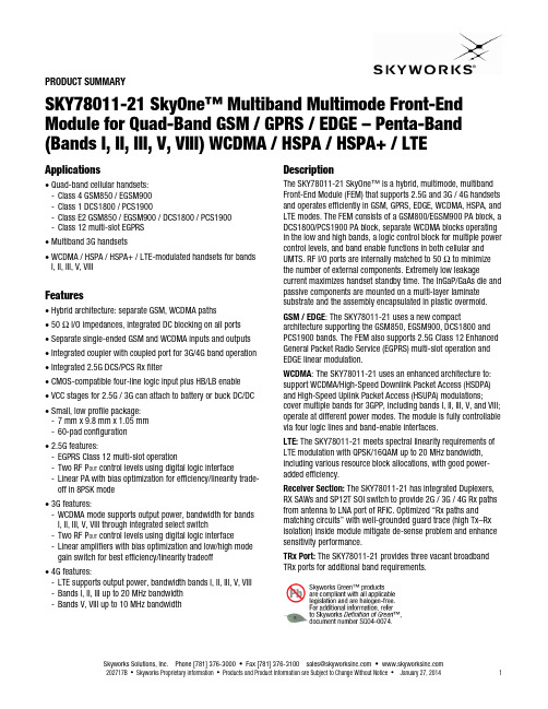
Skyworks Solutions, Inc. Phone [781] 376-3000 • Fax [781] 376-*************************•202717B • Skyworks Proprietary information • Products and Product Information are Subject to Change Without Notice • January 27, 20141PRODUCT SUMMARYSKY78011-21 SkyOne™ Multiband Multimode Front-End Module for Quad-Band GSM / GPRS / EDGE – Penta-Band (Bands I, II, III, V, VIII) WCDMA / HSPA / HSPA+ / LTEApplications• Quad -band cellular handsets: - Class 4 GSM850 / EGSM900 - Class 1 DCS1800 / PCS1900- Class E2 GSM850 / EGSM900 / DCS1800 / PCS1900 - Class 12 multi -slot EGPRS • Multiband 3G handsets• WCDMA / HS PA / HS PA + / LTE-modulated handsets for bands I, II, III, V, VIIIFeatures• Hy brid architecture: separate GSM, WCDMA pa ths • 50 Ω I/O impedances, integrated DC blocking on all ports • Se parate single -ended G S M and WCDMA in puts and out puts • Integrated coupler with coupled port for 3G/4G band operation • Integrated 2.5G DCS/PCS Rx filter• CMOS -c ompatible four-line logic input plus HB/LB enable • VCC stages for 2.5G / 3G can attach to battery or buck DC/DC • Small, low profile package: - 7 mm x 9.8 mm x 1.05 mm - 60-pad configuration• 2.5G features:- E GPRS Class 12 multi -slot operation- Two RF P OUT control levels using digital logic interface- Linear PA with bias optimization for efficiency/linearity trade -off i n 8PSK mode • 3G features:- WCDMA mode supports output power , bandwidth for bands I, II, III, V, VIII through integrated select switch- Two RF P OUT control levels using digital logic interface- Linear amplifiers with bias optimization and low/high mode gain switch for best efficiency/linearity tradeoff • 4G features:- LTE supports output power, bandwidth band s I, II, III, V, VIII - Bands I, II, III up to 20 MHz bandwidth - Bands V, VIII up to 10 MHz bandwidth DescriptionThe SKY78011-21 SkyOne™ is a hybrid, multimode, multiband Front -End Module (FEM) that supports 2.5G and 3G / 4G handsets and operates efficiently in GSM, GPRS, EDGE , WCDMA , HSPA, and LTE modes. The FEM consists of a GSM800/EGSM900 PA block, a DCS1800/PCS1900 PA block, separate WCDMA blocks operating in the low and high bands, a logic control block for multiple power control levels, and band enable functions in both cellular and UMTS. RF I/O ports are internally matched to 50 Ω to minimize the number of external components. Extremely low leakagecurrent maximizes handset standby time. The InGaP/GaAs die and passive components are mounted on a multi -layer laminate substrate and the assembly encapsulated in plastic overmold. GSM / EDGE : The SKY78011-21 uses a new compa ctarchitecture supporting the GSM850, EGSM900, DCS1800 and PCS1900 bands. The FEM also supports 2.5G Class 12 Enhanced General Packet Radio Service (EGPRS) multi -slot operation and EDGE linear modulation.WCDMA : The SKY78011-21 uses an enhanced architecture to : support WCDMA /High -Speed Downlink Packet Access (HSDPA ) and High -Speed Uplink Pa cket Access (HSUPA) modulations ; cover multiple bands for 3GPP , including bands I, II, III, V, and VIII; operate at different power modes . The module is fully controllable via four logic lines and band -enable interfaces.LTE: The SKY78011-21 meets spectral linearity requirements of LTE modulation with QPSK/16QAM up to 20 MHz bandwidth, including various resource block allocations , with good power -added efficiency .Receiver Section: The SKY78011-21 has integrated Duplexers, RX SAWs and SP12T SOI switch to provide 2G / 3G / 4G Rx paths from antenna to LNA port of RFIC. Optimized “Rx paths and matching circuits ” with well-grounded guard trace (high Tx –Rx isolation) inside module mitigate de -sense problem and enhance sensitivity performance.TRx Port: The SKY78011-21 provides three vacant broadband TRx ports for additional band requirements.Ordering InformationProduct Name Order Number Evaluation Board Part Number SKY78011-21 SkyOne™ Multiband Multimode Front-End Module SKY78011-21 —Copyright © 2013, 2014, Skyworks Solutions Inc. All Rights Reserved.Information in this document is provided in connection with Skyworks Solutions Inc. (“Skyworks”) products or services. These materials including the information contained herein are provided by Skyworks as a service to its customers and may be used for informational purposes only by the customer. Skyworks assumes no responsibility for errors or omissions in these materials or the information contained herein. Skyworks may change its documentation products services specifications or product descriptions at any time with out notice. Skyworks makes no commitment to update the materials or information and shall have no responsibility whatsoever for conflicts incompatibilities or other difficulties arising from any future changes.No license whether express implied by estoppel or otherwise is granted to any intellectual property rights by this document. Skyworks assumes no liability for any materials products or information provided hereunder including the sale distribution reproduction or use of Skyworks products information or materials except as may be provided in Skyworks Terms and Conditions of Sale.THE MATERIALS PRODUCTS AND INFORMATION ARE PROVIDED “AS IS” WITH OUT WARRANTY OF ANY KIND WHETHER EXPRESS IMPLIED STATUTORY OR OTHERWISE INCLUDING FITNESS FOR A PARTICULAR PURPOSE OR USE MERCHANTABILITY PERFORMANCE QUALITY OR NON–INFRINGEMENT OF ANY INTELLECTUAL PROPERTY RIGHT; ALL SUCH WARRANTIES ARE HEREBY EXPRESSLY DISCLAIMED. SKYWORKS DOES NOT WARRANT THE ACCURACY OR COMPLETENESS OF THE INFORMATION TEXT GRAPHICS OR OTHER ITEMS CONTAINED WITHIN THESE MATERIALS. SKYWORKS SHALL NOT BE LIABLE FOR ANY DAMAGES INCLUDING BUT NOT LIMITED TO ANY SPECIAL INDIRECT INCIDENTAL STATUTORY OR CONSEQUENTIAL DAMAGES INCLUDING WITH OUT LIMITATION LOST REVENUES OR LOST PROFITS THAT MAY RESULT FROM THE USE OF THE MATERIALS OR INFORMATION WHETHER OR NOT THE RECIPIENT OF MATERIALS HAS BEEN ADVISED OF THE POSSIBILITY OF SUCH DAMAGE.Skyworks products are not intended for use in medical lifesaving or life–sustaining applications or other equipment in which the failure of the Skyworks products could lead to personal injury death physical or environmental damage. Skyworks customers using or selling Skyworks products for use in such applications do so at their own risk and agree to fully indemnify Skyworks for any damages resulting from such improper use or sal e.Customers are responsible for their products and applications using Skyworks products which may deviate from published specifications as a result of design defects errors or operation of products OUT side of published parameters or design specifications. Customers should include design and operating safeguards to minimize these and other risks. Skyworks assumes no liability for applications assistance customer product design or damage to any equipment resulting from the use of Skyworks products OUT side of stated published specifications or parameters. Skyworks, the Skyworks symbol, “Breakthrough Simplicity”, and SkyOne are trademarks or registered trademarks of Skyworks Solutions Inc. in the United States and other countries. Third–pa rty brands and names are for identification purposes only and are the property of their respective owners. Additional information including relevant terms and conditions posted at are incorporated by reference.。
Skyworks SKY77161 PA模块TD-SCDMA(2010-2025MHz)产品概述说明
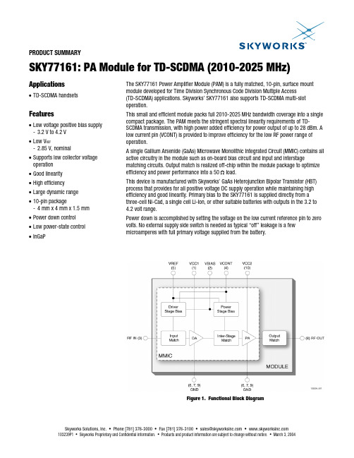
PRODUCT SUMMARYSKY77161: PA Module for TD-SCDMA (2010-2025 MHz)Applications• TD-SCDMA handsetsFeatures• Low voltage positive bias supply - 3.2 V to 4.2 V• Low V REF- 2.85 V, nominal• Supports low collector voltage operation• Good linearity• High efficiency• Large dynamic range• 10-pin package- 4 mm x 4 mm x 1.5 mm • Power down control• Low power-state control• InGaP The SKY77161 Power Amplifier Module (PAM) is a fully matched, 10-pin, surface mount module developed for Time Division Synchronous Code Division Multiple Access(TD-SCDMA) applications. Skyworks’ SKY77161 also supports TD-SCDMA multi-slot operation.This small and efficient module packs full 2010-2025 MHz bandwidth coverage into a single compact package. The PAM meets the stringent spectral linearity requirements of TD-SCDMA transmission, with high power added efficiency for power output of up to 28 dBm. A low current pin (VCONT) is provided to improve efficiency for the low RF power range of operation.A single Gallium Arsenide (GaAs) Microwave Monolithic Integrated Circuit (MMIC) contains all active circuitry in the module such as on-board bias circuit and input and interstage matching circuits. Output match is realized off-chip within the module package to optimize efficiency and power performance into a 50 Ω load.This device is manufactured with Skyworks’ GaAs Heterojunction Bipolar Transistor (HBT) process that provides for all positive voltage DC supply operation while maintaining high efficiency and good linearity. Primary bias to the SKY77161 is supplied directly from a three-cell Ni-Cad, a single cell Li-Ion, or other suitable batteries with outputs in the 3.2 to 4.2 volt range.Power down is accomplished by setting the voltage on the low current reference pin to zero volts. No external supply side switch is needed as typical “off” leakage is a few microamperes with full primary voltage supplied from the battery.Figure 1. Functional Block DiagramSkyworksSolutions,Inc.•Phone[781]376-3000•Fax[781]376-3100•*********************• 103239P1 • Skyworks Proprietary and Confidential information. • Products and product information are subject to change without notice. • March 3, 2004© 2004, Skyworks Solutions, Inc. All Rights Reserved.Information in this document is provided in connection with Skyworks Solutions, Inc. ("Skyworks") products. These materials are provided by Skyworks as a service to its customers and may be used for informational purposes only. Skyworks assumes no responsibility for errors or omissions in these materials. Skyworks may make changes to its products, specifications and product descriptions at any time, without notice. Skyworks makes no commitment to update the information and shall have no responsibility whatsoever for conflicts, incompatibilities, or other difficulties arising from future changes to its products and product descriptions.No license, express or implied, by estoppel or otherwise, to any intellectual property rights is granted by this document. Except as may be provided in Skyworks’ Terms and Conditions of Sale for such products, Skyworks assumes no liability whatsoever.THESE MATERIALS ARE PROVIDED "AS IS" WITHOUT WARRANTY OF ANY KIND, EITHER EXPRESS OR IMPLIED, RELATING TO SALE AND/OR USE OF SKYWORKS™ PRODUCTS INCLUDING WARRANTIES RELATING TO FITNESS FOR A PARTICULAR PURPOSE, MERCHANTABILITY, PERFORMANCE, QUALITY OR NON-INFRINGEMENT OF ANY PATENT, COPYRIGHT OR OTHER INTELLECTUAL PROPERTY RIGHT. SKYWORKS FURTHER DOES NOT WARRANT THE ACCURACY OR COMPLETENESS OF THE INFORMATION, TEXT, GRAPHICS OR OTHER ITEMS CONTAINED WITHIN THESE MATERIALS. SKYWORKS SHALL NOT BE LIABLE FOR ANY SPECIAL, INDIRECT, INCIDENTAL, OR CONSEQUENTIAL DAMAGES, INCLUDING WITHOUT LIMITATION, LOST REVENUES OR LOST PROFITS THAT MAY RESULT FROM THE USE OF THESE MATERIALS.Skyworks™ products are not intended for use in medical, lifesaving or life-sustaining applications. Skyworks’ customers using or selling Skyworks™ products for use in such applications do so at their own risk and agree to fully indemnify Skyworks for any damages resulting from such improper use or sale.The following are trademarks of Skyworks Solutions, Inc.: Skyworks™, the Skyworks symbol, and “Breakthrough Simplicity”™. Product names or services listed in this publication are for identification purposes only, and may be trademarks of third parties. Third-party brands and names are the property of their respective owners.Additional information, posted at , is incorporated by reference.。
OP07官方DataSheet
Ultralow Offset Voltage Operational AmplifierOP07Rev. EInformation furnished by Analog Devices is believed to be accurate and reliable. However , no responsibility is assumed by Analog Devices for its use, nor for any infringements of patents or other rights of third parties that may result from its use. Specifications subject to change without notice. No license is granted by implication or otherwise under any patent or patent rights of Analog Devices. T rademarks and registered trademarks are the property of their respective owners.One Technology Way, P.O. Box 9106, Norwood, M A 02062-9106, U.S.A.Tel: 781.329.4700 Fax: 781.461.3113 ©2006-2009 Analog Devices, Inc. All rights reserved.FEATURESLow V OS : 75 μV maximumLow V OS drift: 1.3 μV/°C maximumUltrastable vs. time: 1.5 μV per month maximum Low noise: 0.6 μV p-p maximumWide input voltage range: ±14 V typical Wide supply voltage range: 3 V to 18 V 125°C temperature-tested diceAPPLICATIONSWireless base station control circuits Optical network control circuits Instrumentation Sensors and controls ThermocouplesResistor thermal detectors (RTDs) Strain bridgesShunt current measurements Precision filtersGENERAL DESCRIPTIONThe OP07 has very low input offset voltage (75 μV maximum for OP07E) that is obtained by trimming at the wafer stage. These low offset voltages generally eliminate any need for externalnulling. The OP07 also features low input bias current (±4 nA for the OP07E) and high open-loop gain (200 V/mV for the OP07E). The low offset and high open-loop gain make the OP07particularly useful for high gain instrumentation applications. PIN CONFIGURATIONV OS TRIMV OS TRIM –IN V++IN OUTV–NCNC = NO CONNECT00316-0011R2A AND R2B ARE ELECTRONICALLY ADJUSTED ON CHIP AT FACTORY FOR MINIMUM INPUT OFFSET VOLTAGE.Figure 1.The wide input voltage range of ±13 V minimum combined with a high CMRR of 106 dB (OP07E) and high inputimpedance provide high accuracy in the noninverting circuit configuration. Excellent linearity and gain accuracy can be maintained even at high closed-loop gains. Stability of offsets and gain with time or variations in temperature is excellent. The accuracy and stability of the OP07, even at high gain, combined with the freedom from external nulling have made the OP07 an industry standard for instrumentation applications.The OP07 is available in two standard performance grades. The OP07E is specified for operation over the 0°C to 70°C range, and the OP07C is specified over the −40°C to +85°C temperature range.The OP07 is available in epoxy 8-lead PDIP and 8-lead narrow SOIC packages. For CERDIP and TO-99 packages and standard microcircuit drawing (SMD) versions, see the OP77.V 600316-002Figure 2. Simplified SchematicOP07Rev. E | Page 2 of 16TABLE OF CONTENTSFeatures .............................................................................................. 1 Applications ....................................................................................... 1 General Description ......................................................................... 1 Pin Configuration ............................................................................. 1 Revision History ............................................................................... 2 Specifications ..................................................................................... 3 OP07E Electrical Characteristics ............................................... 3 OP07C Electrical Characteristics .. (4)Absolute Maximum Ratings ............................................................6 Thermal Resistance .......................................................................6 ESD Caution...................................................................................6 Typical Performance Characteristics ..............................................7 Typical Applications ....................................................................... 11 Applications Information .......................................................... 12 Outline Dimensions ....................................................................... 13 Ordering Guide .. (14)REVISION HISTORY7/09—Rev. D. to Rev EChanges to Figure 29 Caption ....................................................... 11 Changes to Ordering Guide .......................................................... 14 7/06—Rev. C. to Rev D Changes to Features .......................................................................... 1 Changes to General Description .................................................... 1 Changes to Specifications Section .................................................. 3 Changes to Table 4 ............................................................................ 6 Changes to Figure 6 and Figure 8 ................................................... 7 Changes to Figure 13 and Figure 14 ............................................... 8 Changes to Figure 20 ........................................................................ 9 Changes to Figure 21 to Figure 25 ................................................ 10 Changes to Figure 26 and Figure 30 ............................................. 11 Replaced Figure 28 ......................................................................... 11 Changes to Applications Information Section ............................ 12 Updated Outline Dimensions ....................................................... 13 Changes to Ordering Guide . (14)8/03—Rev. B to Rev. CChanges to OP07E Electrical Specifications .................................. 2 Changes to OP07C Electrical Specifications ................................. 3 Edits to Ordering Guide ................................................................... 5 Edits to Figure 6 ................................................................................. 9 Updated Outline Dimensions ....................................................... 11 3/03—Rev. A to Rev. BUpdated Package Titles ...................................................... U niversal Updated Outline Dimensions ....................................................... 11 2/02—Rev. 0 to Rev. A Edits to Features ................................................................................. 1 Edits to Ordering Guide ................................................................... 1 Edits to Pin Connection Drawings ................................................. 1 Edits to Absolute Maximum Ratings .............................................. 2 Deleted Electrical Characteristics .............................................. 2–3 Deleted OP07D Column from Electrical Characteristics ....... 4–5 Edits to TPCs ................................................................................ 7–9 Edits to High-Speed, Low V OS Composite Amplifier . (9)OP07Rev. E | Page 3 of 16SPECIFICATIONSOP07E ELECTRICAL CHARACTERISTICSV S = ±15 V , unless otherwise noted. Table 1.Parameter Symbol Conditions Min Typ Max Unit I NPUT CHARACTERISTICS T A = 25°CInput Offset Voltage 1V OS30 75 μV Long-Term V OS Stability 2V OS /Time 0.3 1.5 μV/Month Input Offset Current I OS 0.5 3.8 nA Input Bias Current I B±1.2 ±4.0 nA Input Noise Voltagee n p-p 0.1 Hz to 10 Hz 3 0.35 0.6 μV p-p Input Noise Voltage Density e nf O = 10 Hz 10.3 18.0 nV/√Hz f O = 100 Hz 3 10.0 13.0 nV/√Hzf O = 1 kHz 9.6 11.0 nV/√Hz Input Noise CurrentI n p-p14 30 pA p-p Input Noise Current Density I n f O = 10 Hz 0.32 0.80 pA/√Hz f O = 100 Hz 3 0.14 0.23 pA/√Hzf O = 1 kHz 0.12 0.17 pA/√Hz Input Resistance, Differential Mode 4R IN 15 50 MΩ Input Resistance, Common Mode R INCM 160 GΩ Input Voltage RangeIVR±13 ±14 V Common-Mode Rejection Ratio CMRR V CM = ±13 V106 123 dB Power Supply Rejection Ratio PSRR V S = ±3 V to ±18 V 5 20 μV/V Large Signal Voltage Gain A VO R L ≥ 2 kΩ, V O = ±10 V200 500 V/mV R L ≥ 500 Ω, V O = ±0.5 V, V S = ±3 V 4150 400 V/mV 0°C ≤ T A ≤ 70°CInput Offset Voltage 1V OS 45 130 μV Voltage Drift Without External Trim 4TCV OS0.3 1.3 μV/°C Voltage Drift with External Trim 3TCV OSN R P = 20 kΩ 0.3 1.3 μV/°C Input Offset CurrentI OS 0.9 5.3 nA Input Offset Current Drift TCI OS 8 35 pA/°C Input Bias CurrentI B ±1.5 ±5.5 nA Input Bias Current Drift TCI B 13 35 pA/°C Input Voltage RangeIVR±13 ±13.5 V Common-Mode Rejection Ratio CMRR V CM = ±13 V103 123 dB Power Supply Rejection Ratio PSRR V S = ±3 V to ±18 V 7 32 μV/V Large Signal Voltage Gain A VOR L ≥ 2 kΩ, V O = ±10 V 180 450 V/mV OUTPUT CHARACTERISTICS T A = 25°COutput Voltage Swing V O R L ≥ 10 kΩ ±12.5 ±13.0 V R L ≥ 2 kΩ ±12.0 ±12.8 VR L ≥ 1 kΩ ±10.5 ±12.0 V 0°C ≤ T A ≤ 70°COutput Voltage Swing V O R L ≥ 2 kΩ ±12 ±12.6 VOP07Rev. E | Page 4 of 16ParameterSymbol Conditions Min Typ Max Unit DY N AMIC PERFORMA NCE T A = 25°CSlew RateSR R L ≥ 2 kΩ30.1 0.3 V/μs Closed-Loop BandwidthBW A VOL = 150.4 0.6 MHz Open-Loop Output Resistance R O V O = 0, I O = 060 Ω Power Consumption P d V S = ±15 V, No load 75 120 mWV S = ±3 V, No load 4 6 mW Offset Adjustment RangeR P = 20 kΩ±4 mV1 Input offset voltage measurements are performed by automated test equipment approximately 0.5 seconds after application of power.2Long-term input offset voltage stability refers to the averaged trend time of V OS vs. the time over extended periods after the first 30 days of operation. Excluding the initial hour of operation, changes in V OS during the first 30 operating days are typically 2.5 μV. Refer to the Typi section. Parameter is sample tested. cal Performance Characteristics 3Sample tested. 4Guaranteed by design. 5Guaranteed but not tested.OP07C ELECTRICAL CHARACTERISTICSV S = ±15 V , unless otherwise noted. Table 2.ParameterSymbol Conditions Min Typ Max UnitINPUT CHARACTERISTICS T A = 25°CInput Offset Voltage 1 V OS 60 150 μV Long-Term V OS Stability 2 V OS /Time 0.4 2.0 μV/Month Input Offset Current I OS 0.8 6.0 nA Input Bias Current I B ±1.8 ±7.0 nA Input Noise Voltagee n p-p 0.1 Hz to 10 Hz 3 0.38 0.65 μV p-p Input Noise Voltage Density e nf O = 10 Hz 10.5 20.0 nV/√Hz f O = 100 Hz 3 10.2 13.5 nV/√Hzf O = 1 kHz 9.8 11.5 nV/√Hz Input Noise Current I n p-p 15 35 pA p-p Input Noise Current Density I n f O = 10 Hz 0.35 0.90 pA/√Hz f O = 100 Hz 3 0.15 0.27 pA/√Hzf O = 1 kHz 0.13 0.18 pA/√Hz Input Resistance, Differential Mode 4 R IN8 33 MΩ Input Resistance, Common Mode R INCM 120 GΩ Input Voltage RangeIVR ±13 ±14 V Common-Mode Rejection Ratio CMRR V CM = ±13 V 100 120 dB Power Supply Rejection Ratio PSRR V S = ±3 V to ±18 V 7 32 μV/V Large Signal Voltage Gain A VO R L ≥ 2 kΩ, V O = ±10 V 120 400 V/mVR L ≥ 500 Ω, V O = ±0.5 V, V S = ±3 V 4100 400 V/mV −40°C ≤ T A ≤ +85°C Input Offset Voltage 1V OS 85 250 μV Voltage Drift Without External Trim 4TCV OS 0.5 1.8 μV/°C Voltage Drift with External Trim 3TCV OSN R P = 20 kΩ 0.4 1.6 μV/°C Input Offset CurrentI OS 1.6 8.0 nA Input Offset Current Drift TCI OS 12 50 pA/°C Input Bias CurrentI B ±2.2 ±9.0 nA Input Bias Current Drift TCI B 18 50 pA/°C Input Voltage RangeIVR ±13 ±13.5 V Common-Mode Rejection Ratio CMRR V CM = ±13 V 97 120 dB Power Supply Rejection Ratio PSRR V S = ±3 V to ±18 V 10 51 μV/V Large Signal Voltage Gain A VO R L ≥ 2 kΩ, V O = ±10 V 100 400 V/mVOP07Rev. E | Page 5 of 16ParameterSymbol Conditions Min Typ Max Unit OUTPUT CHARACTERISTICS T A = 25°COutput Voltage Swing V O R L ≥ 10 kΩ ±12.0 ±13.0 V R L ≥ 2 kΩ ±11.5 ±12.8 VR L ≥ 1 kΩ ±12.0 V −40°C ≤ T A ≤ +85°COutput Voltage Swing V O R L ≥ 2 kΩ ±12 ±12.6 V DYNAMIC PERFORMANCE T A = 25°CSlew RateSR R L ≥ 2 kΩ3 0.1 0.3 V/μs Closed-Loop BandwidthBW A VOL = 15 0.4 0.6 MHz Open-Loop Output Resistance R O V O = 0, I O = 060 Ω Power Consumption P d V S = ±15 V, No load 80 150 mWV S = ±3 V, No load 4 8 mW Offset Adjustment RangeR P = 20 kΩ±4mV1 Input offset voltage measurements are performed by automated test equipment approximately 0.5 seconds after application of power.2Long-term input offset voltage stability refers to the averaged trend time of V OS vs. the time over extended periods after the first 30 days of operation. Excluding the initial hour of operation, changes in V OS during the first 30 operating days are typically 2.5 μV. Refer to the Typi section. Parameter is sample tested. cal Performance Characteristics 3Sample tested. 4Guaranteed by design. 5Guaranteed but not tested.OP07Rev. E | Page 6 of 16ABSOLUTE MAXIMUM RATINGSTable 3.Parameter Ratings Supply Voltage (V S ) ±22 V Input Voltage 1±22 V Differential Input Voltage ±30 V Output Short-Circuit Duration Indefinite Storage Temperature Range S and P Packages −65°C to +125°COperating Temperature RangeOP07E 0°C to 70°COP07C −40°C to +85°CJunction Temperature 150°C Lead Temperature, Soldering (60 sec) 300°C1For supply voltages less than ±22 V, the absolute maximum input voltage is equal to the supply voltage.Stresses above those listed under Absolute Maximum Ratingsmay cause permanent damage to the device. This is a stress rating only; functional operation of the device at these or anyother conditions above those indicated in the operational section of this specification is not implied. Exposure to absolute maximum rating conditions for extended periods may affect device reliability. THERMAL RESISTANCE θJA is specified for the worst-case conditions, that is, a device soldered in a circuit board for surface-mount packages. Table 4. Thermal Resistance Package Type θJA θJC Unit8-Lead PDIP (P-Suffix) 103 43 °C/W 8-Lead SOIC_N (S-Suffix) 158 43 °C/WESD CAUTIONESD (electrostatic discharge) sensitive device. Electrostatic charges as high as 4000 V readily accumulate on the human body and test equipment and can discharge without detection. Although this product features proprietary ESD protection circuitry, permanent damage may occur on devices subjected to high energy electrostatic discharges. Therefore, proper ESD precautions are recommended to avoid performancedegradation or loss of functionality.OP07Rev. E | Page 7 of 16–50–75100500–251257525TYPICAL PERFORMANCE CHARACTERISTICS10000200400600800900100300500700O P E N -L O O P G A I N (V /m V )TEMPERATURE (°C)00 1.00.80.60.40.201001k10k100kMATCHED OR UNMATCHED SOURCE RESISTANCE (Ω)M A X I M U M E R R O R R E F E R R E D T O I N P U T(m V )00316-006316-003Figure 3. Open-Loop Gain vs. Temperature302520151050A B S O L U T E C H A N G E I N I N P U T O F F S E T V O L T A G E (µV )–20020406080100TIME (Seconds)316-00400Figure 4. Offset Voltage Change due to Thermal ShockOP07COP07E252015105A B S O L U T E C H A N G E I N I N P U T O F F S E T V O L T A G E (µV )V S = ±15V T A = 25°CFigure 6. Maximum Error vs. Source Resistance1.21.00.80.60.40.201001k10k100kMATCHED OR UNMATCHED SOURCE RESISTANCE (Ω)M A X I M U M E R R O R R E F E R R E D T O I N P U T (m V )00316-007Figure 7. Maximum Error vs. Source Resistance30–30–20–101020–30–20–103020100N O N I N V E R T I N G I N P U T B I A SC U R R E N T (n A )012345TIME AFTER SUPPLY TURN-ON (Minutes)00316-005Figure 5. Warm-Up Drift DIFFERENTIAL INPUT VALUE (V)316-00800Figure 8. Input Bias Current vs. Differential Input VoltageOP07Rev. E | Page 8 of 164321I N P U T B I A S C U R R E N T (n A )0TEMPERATURE (°C)–50–75100500–25125752500316-009Figure 9. Input Bias Current vs. Temperature2.52.01.51.00.50TEMPERATURE (°C)–50–100–75500–251007525I N P U T O F F S E T C U R RE N T (n A )00316-010Figure 10. Input Offset Current vs. TemperatureTIME (1s/DIV)V O L T A G E (200n V /D I V )00316-0111000100101FREQUENCY (Hz)I N P U T N O I S E V O L T A G E (n V H z )1011000100Figure 11. Low Frequency Noise 00316-012Figure 12. Total Input Noise Voltage vs. Frequency1010.1BANDWIDTH (Hz)R M S N O I S E (µV )1k 100100k10k00316-013Figure 13. Input Wideband Noise vs. Bandwidth,0.1 Hz to Frequency Indicated130120110100908070C M R R (d B )60FREQUENCY (Hz)101100k1k10k10000316-014Figure 14. CMRR vs. FrequencyOP07Rev. E | Page 9 of 1612011010090807060P S R R (d B )10080604020–20FREQUENCY (Hz)C L O S ED -L O O P G A I N (d B )101001k 10k 100k 1M 10M50FREQUENCY (Hz)100.1110k 1k 1001000800600400200O P E N -L O O P G A I N (V /m V )20T A = 25°C00316-015Figure 15. PSRR vs. FrequencyPOWER SUPPLY VOLTAGE (V)±100±5±±1500316-016Figure 16. Open-Loop Gain vs. Power Supply Voltage00316-018120100806040200–20–40FREQUENCY (Hz)O P E N -L O OP G A I N (d B )0.11101001k 10k 100k 1M 10M 00316-017Figure 17. Open-Loop Frequency Response Figure 18. Closed-Loop Frequency Response for Various Gain Configurations2824201612840FREQUENCY (Hz)P E A K -T O -P E A K A M PL I T U D E (V )1k10k 100k1M00316-019Figure 19. Maximum Output Swing vs. Frequency2015105M A X I M U MO U T P U T (V )0LOAD RESISTANCE TO GROUND (Ω)1001k10k00316-020Figure 20. Maximum Output Voltage vs. Load ResistanceOP07Rev. E | Page 10 of 161000100101TOTAL SUPPLY VOLTAGE, V+ TO V– (V)0102030405060P O W E R C O N S UM P T I O N (m W )00316-021Figure 21. Power Consumption vs. Power Supply3530252015TIME FROM OUTPUT BEING SHORTED (Minutes)04321O U T P U T S H O R T -C I R C U I T C U R R E N T (m A)00316-022Figure 22. Output Short-Circuit Current vs. Time85.0042.5063.7521.25O L U T E V A L U E O F O F F S E T V O L T A G E (µV )0TEMPERATURE (°C)A B S–751251007550250–25–5000316-02330.015.022.57.50TEMPERATURE (°C)A B S O L U T E V A L U E O F O F F S E T V O L T A G E (µV )–100–751007550250–25–50Figure 23. Untrimmed Offset Voltage vs. Temperature00316-02416–16–12–8–404812TIME (Months)T O T A L D R I F T W I T H T I M E (µV )0121110987654321Figure 24. Trimmed Offset Voltage vs. Temperature00316-025Figure 25. Offset Voltage Drift vs. TimeTYPICAL APPLICATIONSE OE INE O = –E IN –I BRFRF R100316-026Figure 26. Typical Offset Voltage Test CircuitE OE 3E 2E 1R410k Ω00316-027Figure 27. Typical Low Frequency Noise Circuit OUTV+00316-028Figure 28. Optional Offset Nulling CircuitE OR5R4R3E IN ±10V0316-0290Figure 29. Absolute Value CircuitE OE INO IN B RF R1NOTES1. PINOUT SHOWN FOR P PACKAGE00316-030Figure 30. High Speed, Low V OS Composite AmplifierE OE 3E 2E 1R410k ΩNOTES1. PINOUT SHOWN FOR P PACKAGE00316-031Figure 31. Adjustment-Free Precision Summing AmplifierNOTES1. PINOUT SHOWN FOR P PACKAGEE OREFERENCE JUNCTIONSENDING JUNCTION00316-032Figure 32. High Stability Thermocouple AmplifierE OR510k ΩR410k ΩR310k ΩE IN ±10VNOTES1. PINOUT SHOWN FOR P PACKAGE00316-033Figure 33. Precision Absolute-Value CircuitAPPLICATIONS INFORMATIONThe OP07 provides stable operation with load capacitance of up to 500 pF and ±10 V swings; larger capacitances should be decoupled with a 50 Ω decoupling resistor.Stray thermoelectric voltages generated by dissimilar metals at the contacts to the input terminals can degrade driftperformance. Therefore, best operation is obtained when both input contacts are maintained at the same temperature, preferably close to the package temperature.(IN PARENTHESES)ARE ROUNDED-OFF MILLIMETER EQUIVALENTS FOR REFERENCE ONLY AND ARE NOT APPROPRIATE FOR USE IN DESIGN.060506-AOUTLINE DIMENSIONSCONTROLLING DIMENSIONS ARE IN MILLIMETERS; INCH DIMENSIONS COMPLIANT TO JEDEC STANDARDS MS-012-AA0.25 (0.0098)0.17 (0.0067)0.40 (0.0157)45°0.25 (0.0098)0.10 (0.0040)COPLANARITY0.10Figure 34. 8-Lead Standard Small Outline Package [SOIC_N]Narrow Body S-Suffix(R-8)Dimensions shown in millimeters and (inches)COMPLIANT TO JEDEC STANDARDS MS-001CONTROLLING DIMENSIONS ARE IN INCHES; MILLIMETER DIMENSIONS A(IN PARENTHESES)ARE ROUNDED-OFF INCH EQUIVALENTS FORREFERENCE ONLY AND ARE NOT APPROPRIATE FOR USE IN DESIGN.CORNER LEADS MAY BE CONFIGURED AS WHOLE OR HALF LEADS.070606-0.060 (1.52)0.045 (1.14)BSCMAX0.325 (8.26)0.310 (7.87)0.015 (0.38)GAUGE PLANEFigure 35. 8-Lead Plastic Dual-in-Line Package [PDIP]P-Suffix (N-8)Dimensions shown in inches and (millimeters)ORDERING GUIDEPackage Description Package OptionRangeodel TemperatureOP07EP 0°C to 70°C 8-Lead PDIP N-8 (P-Suffix) OP07EPZ10°C to 70°C 8-Lead PDIP N-8 (P-Suffix) OP07CP 0°C to 70°C 8-Lead PDIP N-8 (P-Suffix) OP07CPZ1−40°C to +85°C 8-Lead PDIP N-8 (P-Suffix) OP07CS −40°C to +85°C 8-Lead SOIC_N R-8 (S-Suffix) OP07CSZ1−40°C to +85°C 8-Lead SOIC_N R-8 (S-Suffix) OP07CSZ-REEL1−40°C to +85°C 8-Lead SOIC_N R-8 (S-Suffix) OP07CSZ-REEL71−40°C to +85°C 8-Lead SOIC_N R-8 (S-Suffix)1 Z = RoHS Compliant Part.NOTESNOTES©2006-2009 Analog Devices, Inc. All rights reserved. Trademarks andregistered trademarks are the property of their respective owners.D00316-0-7/09(E)。
- 1、下载文档前请自行甄别文档内容的完整性,平台不提供额外的编辑、内容补充、找答案等附加服务。
- 2、"仅部分预览"的文档,不可在线预览部分如存在完整性等问题,可反馈申请退款(可完整预览的文档不适用该条件!)。
- 3、如文档侵犯您的权益,请联系客服反馈,我们会尽快为您处理(人工客服工作时间:9:00-18:30)。
Sky WAN®技术指标
网络类型
拓扑结构全网状、星状、混合状
卫星信道访问MF-TDMA多载波跳频,支持跨转发器和交叉
转发器操作
卫星信道分配BOD动态带宽按需分配,支持实时和非实时应
用,保证吞吐量及QoS服务优先等级
室内单元(IDU)
Modem速率64K~5M波特(64Kbps~8.75Mbps),每波特连续
可调,各载波速率独立设置,支持跳频跳速
调制方式QPSK
FEC前向纠错码率1/2、3/4、7/8
前向纠错方式卷积、RS级联编码及维特比译码
中频频率L频段,支持575MHz卫星全带宽访问
IDU接口4个串行接口和1个以太网/快速以太网接口
用户接口和业务
内置IP路由器
物理接口10/100Mbps以太网接口,IEEE 802.3,RJ-45 协议规程静态路由、OSPF动态路由、IP组播;
TCP、TCP加速、UDP、IGMP、V oIP、IP QoS、
DiffServ、ROHC强劲包头压缩;
V oIP和IP实时视频白金动态级QoS
内置帧中继交换机
物理接口X.21、RS-449、RS-232C和V.35
协议规程帧中继、UNI(用户-网络接口)、NNI(网络-网络
接口)、比特同步透明数据传输
数据速率~ 6Mbps
Sky WAN® FAD话音和数据
模拟话音/传真接口FXS、FXO和E&M标准
数字话音接口和信令E1/T1(G.703),CAS、R2 QSIG、中国1号信令
ISDN BRI/PRI
GSM接口和信令A-bis、A-ter、A、E、SS-7,自适应带宽优化话音压缩8Kbps ACELP及其它选项
传真G3传真,2.4Kbps ~ 14.4Kbps
串行数据接口 1 ~ 3个,可扩展
串行数据速率~ 6Mbps
串行数据协议规程HDLC、SDLC、异步、BSC、比特透明
局域网接口双10/100Mbps以太网接口,IEEE 802.3
Sky WAN®技术指标(续)
室外单元(ODU)
Ku频段RFT 5000:8、20、30瓦
RFT 2000:2、4瓦
C频段RFT 5000:10、20、40瓦
RFT 2000:5瓦
电源RFT 5000:交流90~260V或直流48V
RFT 2000:由IDU 2000内置直流模块供电
网络管理系统(NMS)
NMS平台Sky NMS
NMS布局中心站+任意站点异地备份(选项)
IDU管理接口❖SNMP远程带内管理访问(由中心站NMS通
过卫星网)
❖远程拨号访问(由Modem通过公用电话网)
❖本地访问(通过IDU内置控制端口EIA-232) 电气和机械
尺寸Sky WAN® IDU 5000
Sky WAN® IDU 2500/2000 4U(高) x 483毫米(宽,19") x 470毫米(深) 2U(高) x 483毫米(宽,19") x 470毫米(深)
重量Sky WAN® IDU 5000
Sky WAN® IDU 2500/2000 11.2公斤(5枚插卡满配置) 7.0公斤(3枚插卡满配置)
IDU供电100~240V±10%自动感测
输入频率47~63Hz
认证IEC 60950 CB体系,符合欧洲标准,满足安全
性、电磁兼容性、R&TTE(无线电和电信终端
设备),以及中国国家无线电管理委员会等方面
的规定。