LMZ10505
LMZ10503

5
LMZ10503
典型性能特性
时的波形和效率曲线。
除非另有规定,否则以下条件适用于:VIN=VEN=5.0V, CIN是47 μF 10V X5R 陶瓷电容器;TAMBIENT = 25℃
负载瞬态响应
VIN = 3.3V, VOUT = 2.5V, IOUT = 0.3A至2.7A至0.3A阶跃 20兆赫兹带宽限制
7
负载(A)
30111867
LMZ10503
负载(A)
电流降额 VIN = 5V, θJA = 20°C / W
LMZ10503
2010年6月10日
具备5.5V最高输入电压的3A SIMPLE SWITCHER® 电源模块
易于使用的7引脚封装
顶视图
底视图
TO-PMOD 7引脚封装
10.16x13.77x4.57mm(0.4x0.39x0.18英寸) θJA=20℃/W, θJC =1.9℃/W(注释3 ) 符合RoHS(危害物质限用指令)标准
订购信息
订购号 LMZ10503TZE-ADJ LMZ10503TZ-ADJ LMZ10503TZX-ADJ
顶视图 7引脚TO-PMOD
供货方式 每排45件 250件,卷带封装 500件,卷带封装
封装类型 TO-PMOD-7
30111872
NSC封装图纸 TZA07A
封装标识 LMZ10503TZ-ADJ
工作结温范围-40℃至+125℃ ■ 采用整块的裸露焊盘和标准引脚,更易于装配和制造 ■ 引脚到引脚兼容设计:
LMZ10504(最大4A/20W) LMZ10505(最大5A/25W) ■ 可得到WEBENCH® 和电源设计软件的全面支持
银玛绿光激光打标机
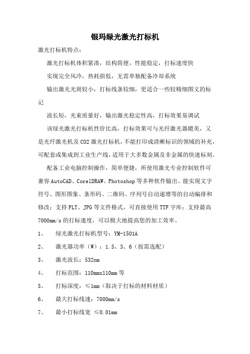
银玛绿光激光打标机
激光打标机特点:
激光打标机体积紧凑,结构简便,性能稳定,打标速度快
实现完全风冷,热耗损低,无需单独配备冷却系统
输出激光光斑较小,打标线条较细,更适合一些较精细图文的标
记
波长短,光束质量好,输出激光稳定性高,打标效果易调试
该绿光激光打标机性价比高,打标效果可与光纤激光器媲美,又
是光纤激光机及CO2激光打标机,不能打印成清晰标识的领域的补充,可配套或集成到工业生产线,适用于大多数金属及非金属的快速标刻。
配备工业电脑控制操作,简单便捷,所使用激光专业控制软件可
兼容AutoCAD、CorelDRAW、Photoshop等多种软件输出。
能实现文字符号、图形图象、条形码、二维码、序列号自动递增等的自动编排和修改;支持PLT、JPG等文件格式,可直接使用TTF字库;支持最高7000mm/s的打标速度,可以极大地提高您的加工效率。
1、绿光激光打标机型号:YM-1501A
2、激光器功率(W):1.5、
3、6(按需选配)
3、激光波长:532nm
4、打标范围:110mmx110mm等
5、打标深度:≤1mm(取决于打标的材料材质)
6、最大打标线速:7000mm/s
7、最小打标线宽≤0.01mm
8、最小字符高度:0.2mm
9、重复打标精度≤10μrad
10、打标形式:静态
11、耗电功率≤0.8KW
12、电力需求:220VAC/50Hz
13、工作环境:4-40°C,相对湿度:≤85%
14、整机尺寸:650*500*1650mm
2、应用行业:汽车配件、玻璃制品、水果、鸡蛋、电子元器件、集成电路(IC)、电工电器、通讯产品、标牌。
LM10线性磁编码器系统数据表说明书
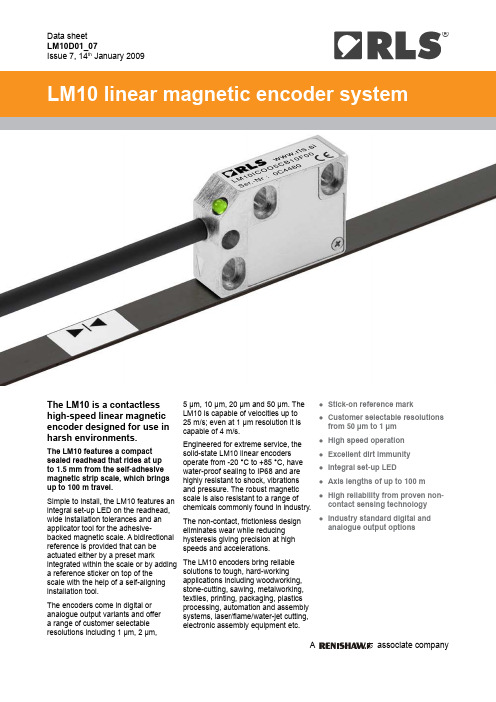
®Data sheet LM10D01_07Issue 7, 14thJanuary 2009The LM10 is a contactless high-speed linear magnetic encoder designed for use in harsh environments.The LM10 features a compact sealed readhead that rides at up to 1.5 mm from the self-adhesive magnetic strip scale, which brings up to 100 m travel.Simple to install, the LM10 features an integral set-up LED on the readhead, wide installation tolerances and an applicator tool for the adhesive-backed magnetic scale. A bidirectional reference is provided that can be actuated either by a preset markintegrated within the scale or by adding a reference sticker on top of thescale with the help of a self-aligninginstallation tool.The encoders come in digital or analogue output variants and offer a range of customer selectable resolutions including 1 µm, 2 µm,5 µm, 10 µm, 20 µm and 50 µm. The LM10 is capable of velocities up to 25 m/s; even at 1 µm resolution it is capable of 4 m/s.Engineered for extreme service, thesolid-state LM10 linear encoders operate from -20 °C to +85 °C, have water-proof sealing to IP68 and are highly resistant to shock, vibrations and pressure. The robust magnetic scale is also resistant to a range of chemicals commonly found in industry.The non-contact, frictionless design eliminates wear while reducinghysteresis giving precision at high speeds and accelerations.The LM10 encoders bring reliablesolutions to tough, hard-working applications including woodworking, stone-cutting, sawing, metalworking, textiles, printing, packaging, plasticsprocessing, automation and assembly systems, laser/flame/water-jet cutting, electronic assembly equipment etc.Stick-on reference mark●Customer selectable resolutions ●from 50 µm to 1 µm High speed operation ●Excellent dirt immunity ●Integral set-up LED ●Axis lengths of up to 100 m ●High reliability from proven non- ●contact sensing technology Industry standard digital and ●analogue output optionsData sheetLM10D01_07Dimensions and tolerances in mm.LM10 dimensionsLM10 installation tolerancesRide height0.1 - 1.5 mm®Maximum measuring length 50 m (100 m special order)Pole length2 mmAvailable resolution for digital outputs 1 µm, 2 µm, 5 µm, 10 µm, 20 µm and 50 µm Sinusoidal period length 2 mmMaximum speedFor analogue voltage and analogue current output: 25 m/s Sensor/magnetic scale gap With periodic or machined reference: 0.1 to 1.5 mm With stick-on reference: 0.5 to 1.5 mm Error band±40 µm at 20 °C Linear expansion coefficient ~ 17 × 10-6/KRepeatability Better than unit of resolution for movement in the same direction Hysteresis*< 3 µm up to 0.2 mm ride height Sub divisional error±3.5 µm for < 0.7 mm ride height (to ensure SDE remains under ±3.5 µm order option 01 that provides alarm and red LED at 0.7 mm ride height)±7.5 µm for 1 mm ride height Cable PUR high flexible cable, drag-chain compatible, double-shielded 8 × 0.05 mm 2; durability: 20 million cycles at 20 mm bend radiusReadhead (1 m cable, no connector) 56.4 g, Magnetic scale (1 m) 60 g, Cover foil (1 m) 3.5 gPower supply4.7 V to 7 V – reverse polarity protected; voltage on readhead Power consumption (without any load)< 30 mA for digital output type < 50 mA for analogue output types Voltage drop over cable 13 mV/m – without load 54 mV/m – with 120 Ω loadOutput signalsDigital – Open Collector NPN, Differential RS422, short circuit protected TemperatureOperating -10 °C to +80 °C (cable under non-dynamic conditions: -20 °C to +85 °C)Storage-40 °C to +85 °CEnvironmental sealing IP68 (according to IEC 60529)EMC ImmunityIEC 61000-6-2 (particularly: ESD: IEC 61000-4-2; EM fields: IEC 61000-4-3; Burst: IEC 61000-4-4; Surge: IEC 61000-4-5; Conducted disturbances: IEC 61000-4-6; Power frequency magnet fields: IEC 61000-4-8; Pulse magnetic fields: IEC 61000-4-9)EMC InterferenceIEC 61000-6-4 (for industrial, scientific and medical equipment: IEC 55011)Vibrations (55 Hz to 2000 Hz)300 m/s 2 (IEC 60068-2-6)Shocks (11 ms)300 m/s 2 (IEC 60068-2-27)LM10 technical specifications* Repeatable, and can be measured and compensated once installedData sheetLM10D01_07A B ZA B ZSquare wave differential line driver to EIA RS422NOTE : Set-up LED in the case of poor signal strenght is flashing red.LM10IC – Digital output signals, RS422Power supply voltage 4.7 V to 7 V – reverse polarity protected; voltage on readhead *Reverse polarity protectionIncremental signals2 square-wave signals A, B and their inverted signals A-, B-Reference signal 1 or more square-wave pulse Z and its inverted pulse Z-Signal levelDifferential line driver to EIA standard RS422:U H ≥ 2.5 V at -I H = 20 mA U L ≤ 0.5 V at I L = 20 mAPermissible loadZ O ≥ 100 Ω between associated outputs I L ≤ 20 mA max. load per output Capacitive load ≤ 1000 pFOutputs are protected against short circuit to 0 V and to +5 VAlarmHigh impedance on output lines A, B, A-, B-Switching time (10 to 90 %)t+, t- < 30 ns (with 1 m cable and recommended input circuit)Cable lengthmax. 100 mTiming diagramComplementary signals not shownRecommended signal terminationRecommended signal terminationSquare wave outputLM10IB – Digital output signals, Open Collector NPNPower supply voltage 5 V to 30 V Powerconsumption 30 mA Output signals A, B, ZReference signal 1 or more square-wave pulses Z Maximum load 20 mA Cablemax. 10 mTiming diagram* Please consider voltage drop over cable.®2 channels V1and V2differential sinusoidals (90° phase shifted)Timing diagramLM10AV – Analogue output signals (1 Vpp)Power supplyvoltage4.7 V to 7 V – reverse polarity protected;voltage on readhead *Reverse polarity protectionIncrementalsignalsAmplitude(with 120 Ω termination)0.6 Vppto 1.2 VppPhase shift90° ± 0.5°Reference signal Amplitude(with 120 Ω termination)0.8 Vppto 1.2 VppPosition45°Width45°Termination ZO= 120 Ω between associated outputsCable length max. 50 m(V1+) - (V1-)(V2+) - (V2-)(V+) - (V-) - 1.2 VppΩ0.6 Vpp- 1.2 Vppwith 120 Ωtermination0 V0 V0 V2 channels I1and I2sinusoidals (90° phase shifted)LM10AC – Analogue micro current output signals (12 µA)Power supplyvoltage4.7 V to 7 V – reverse polarity protected;voltage on readhead *Reverse polarity protectionIncrementalsignalsAmplitude7 µA to 16 µAPhase shift90° ± 0.5°Reference signal Amplitude8 µA to 12 µAPosition45°Width45°Cable length max. 10 mI1I2I0 µA0 µA0 µATiming diagram* Please consider voltage drop over cable.* Please consider voltage drop over cable.Reference markSet-up LEDProgrammingPositive direction3) Every 2 mm. The LM10 readhead should be ordered with this specific mode activated only.After the installation of the magnetic scale (see LM10 Installation guide) the readhead can be easily adjusted on the machine using the set-up LED indicator.Digital output signals – A leads BAnalogue output signals (1 V pp ) – V 1 leads V 2Analogue output signals (12 µA) – I 1 leads I 2A, B, A-, B- outputs become high impedance programming interface.NOTE : IB output type: LED flashes red.LM10 IC 010 CA 10 F 00LM10 readhead part numberingMinimum edge separation For AV and AC output types A - N/AFor IB and IC output types A - 0.12 µs (8.3 MHz)*B - 0.5 µs (2 MHz)C - 1 µs (1 MHz)D - 2 µs (0.5 MHz)E - 4 µs (0.25 MHz)ReferenceA - With referenceB - No referenceC - Periodic as per scale pitch (2 mm)Cable length10 - 1.0 m (standard)Connector option A - 9 pin D type plugB - 15 pin D type socket (for IC output type)D - 15 pin D type plug (for IC output type)L - 15 pin D type plug (for AV output type)F - Flying lead (no connector)Special requirements00 - No special requirements (standard)01 - 0.7 mm ride height alarmOutput typeIB - Incremental, Open Collector NPN; 5 V - 30 V IC - Incremental, RS422; 5 V AV - Analogue voltage, 1 V pp ; 5 V AC - Analogue micro current, 12 µA; 5 VResolution000 - for AV and AC output typesFor IB and IC output types 001 - 1 µm 002 - 2 µm 005 - 5 µm 010 - 10 µm 020 - 20 µm 050 - 50 µmPRG - Programmable from 1 µm to 50 µm (preset to 1 µm)LM10 system ReadheadScaleReadhead part number eg LM10IC010CA10F00Magnetic scale part number eg MS10B1000B0032RLS d.o.o. reserves the right to change specifications without notice.* Default for PRG option.+=CF10 1000MS10 B 1000 B 0032Positive counting30 mm10 mmMachined reference mark (Ri)Position of reference markMin. distance of Ri from left edgeMin. distance of Ri from rightedgeTape length = measuring length + 25 mmMeasuring lengthMagnetic scale part numberingAccessories part numberingCover foilFoil lengthxxxx - Where xxxx equals foil length in cmStick-on reference mark LM10SRM00Applicator tool for stick-on reference markLM10ARM00Applicator tool for magnetic scale and cover foil LM10ASC00End clamp kit (2 clamps + 2 screws)LM10ECL00Precision class B - 40 µm/mTape lengthxxxx - Where xxxx equals tape length in cmCover foilA - No cover foilB - Cover foil supplied (separately - 5 cm longer than tape)C - No cover foil, ends prepared for end clampingPosition of reference mark 0000 - No reference markxxxx - Where xxxx equals position of machined referencemark in cmNOTE: Reference mark position will be within ±1 cm fromrequested position.NOTE: tape length = measuring length + 25 mmRLS d.o.o. has made considerable effort to ensure the content of this document is correct at the date of publication but makes no warranties orrepresentations regarding the content. RLS d.o.o. excludes liability, howsoever arising, for any inaccuracies in this document. © 2009 RLS d.o.o.RLS merilna tehnika d.o.o.Cesta II. grupe odredov 25SI-1261 Ljubljana - Dobrunje SloveniaT +386 1 5272100F +386 1 5272129E ***********www.rls.siHead officeAustraliaT +61 3 9521 0922E **********************AustriaT +43 2236 379790E ********************BrazilT +55 11 4195 2866E *******************CanadaT +1 905 828 0104E *******************The People’s Republic of China T +86 10 8448 5306E ********************Czech Republic T +420 5 4821 6553E ******************FranceT +33 1 64 61 84 84E *******************GermanyT +49 7127 9810E ********************Hong KongT +852 2753 0638E *********************HungaryT +36 23 502 183E ********************IndiaT +91 20 6674 6751E ******************IsraelT +972 4 953 6595E *******************ItalyT +39 011 966 10 52E ******************JapanT +81 3 5366 5316E ******************The Netherlands T +31 76 543 11 00E ********************PolandT +48 22 577 11 80E *******************RussiaT +7 495 231 1677E *******************SingaporeT +65 6897 5466E **********************SloveniaT +386 1 52 72 100E ***********South KoreaT +82 2 2108 2830E ***********************SpainT +34 93 663 34 20E ******************SwedenT +46 8 584 90 880E *******************SwitzerlandT +41 55 415 50 60E ************************TaiwanT +886 4 2473 3177E *******************UKT +44 1453 524524E ***************USAT +1 847 286 9953E ****************For all other countries Please contact RLS’ head officeT +386 1 52 72 100E ***********IssueDatePageCorrections made0229.11.2007-Minor text errors corrected, Corrected Maximum speed table data on page 330.11.20072Changed Pitch and Yaw description and image layout 15. 1. 20083, 4, 5Minor text errors corrected 0328. 2. 20081, 3, 7Removed the 100 µm option2Added the Reference mark detection side symbol 5 New reference mark images8Added the magnetic scale dimensions image 04 6. 6. 20082, 5New installation drawing-Reference mark installation moved to LM10 Installation guide 4, 6Analogue output signal specifications added6IB output type removed, AC output type and connector option L added 0525. 11. 20084, 7, 8IB output type, new magnetic scale diagram and end clamping option added 06 5. 12. 20083Hysteresis data added 0714. 1. 2009-New layoutDocument issues。
LMZ10505EXTTZNOPB;LMZ10505EXTTZXNOPB;LMZ10505EXTTZENOPB;中文规格书,Datasheet资料

PRODUCTION DATA information is current as of
publication date. Products conform to specifications per
the terms of the Texas Instruments standard warranty.
EN61000 4-3
● Passes vibration standard
MIL-STD-883 Method 2007.2 Condition A JESD22-B103B Condition 1
● Passes drop standard
MIL-STD-883 Method 2002.3 Condition B JESD22-B110 Condition B
Key Features
● Integrated shielded inductor ● Flexible startup sequencing using external soft-start,
tracking, and precision enable
● Protection against in-rush currents and faults such as input
-65°C to 150°C
Peak Reflow Case Temperature (30 sec)
245°C
For soldering specifications, refer to the following document: /lit/snoa549c
Operating Ratings (Note 5)
Performance Benefits
● Operates at high ambient temperatures ● Low radiated emissions (EMI) complies with EN55022
LMZ1-0.5型电流互感器 说明书
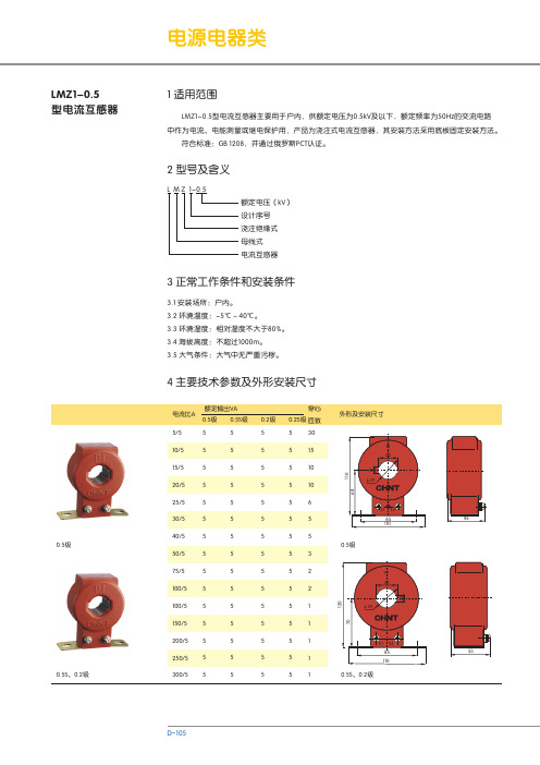
0.5级 0.5S、0.2级
电源电器类
1 适用范围
LMZ1-0.5型电流互感器主要用于户内,供额定电压为0.5kV及以下,额定频率为50Hz的交流电路 中作为电流、电能测量或继电保护用,产品为浇注式电流互感器,其安装方法采用底板固定安装方法。
符合标准:GB 1208,并通过俄罗斯PCT认证。
2 型号及含义
L M Z 1-0.5
额定电压(kV) 设计序号 浇注绝缘式 母线式 电流互感器
3 正常工作条件和安装条件
3.1 安装场所:户内。 3.2 环境温度:-5℃~40℃。 3.3 环境湿度:相对湿度不大于80%。 3.4 海拔高度:不超过1000m。 3.5 大气条件:大气中无严重污秽。
4 主要技术参数及外形安装尺寸
额定输出VA 电流比A
0.5级 0.5S级
5/5
5
5
0.2级 5
穿心 0.2S级 匝数 5 30
10/5
5
5
5
5 15
15/5
5
5
5
5 10
20/5
5
5
5
5 10
外形及安装尺寸
P1 32 φ29
110 68
10
25/5
5
5
5
56
S1 S2
30/5
5
5
5
55
85
46
110
40/5
5
5
50/5
5
5
5
55
例如:订货LMZ1-0.5型,电流比150/5A、额定输出5VA、准确级0.5级的互感器。 订货代号为:LMZ1-0.5 150/5A 5VA 0.5级 5.4 如有特殊要求时,可与厂家协商定制。
英飞凌 FZ1500R33HL3 IHM-B 模块 数据表
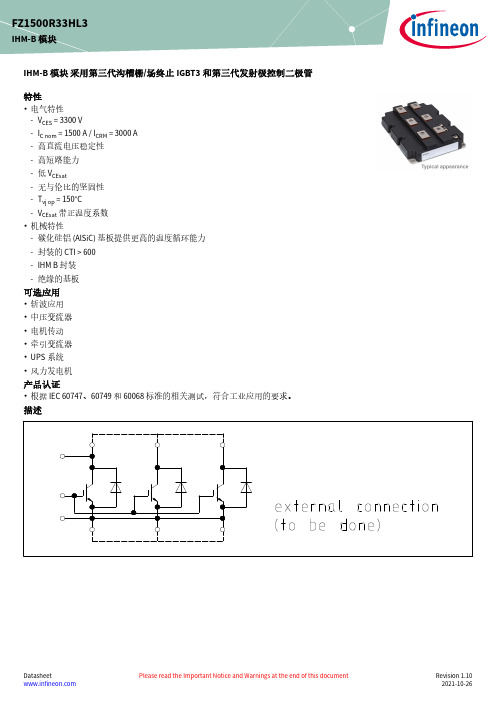
IHM-B 模块 采用第三代沟槽栅/场终止IGBT3和第三代发射极控制二极管特性•电气特性-V CES = 3300 V-I C nom = 1500 A / I CRM = 3000 A -高直流电压稳定性-高短路能力-低 V CEsat-无与伦比的坚固性-T vj op = 150°C -V CEsat 带正温度系数•机械特性-碳化硅铝 (AlSiC) 基板提供更高的温度循环能力-封装的 CTI > 600-IHM B 封装-绝缘的基板可选应用•斩波应用•中压变流器•电机传动•牵引变流器•UPS 系统•风力发电机产品认证•根据 IEC 60747、60749 和 60068标准的相关测试,符合工业应用的要求。
描述FZ1500R33HL3IHM-B 模块内容描述 . . . . . . . . . . . . . . . . . . . . . . . . . . . . . . . . . . . . . . . . . . . . . . . . . . . . . . . . . . . . . . . . . . . . . . . . . . . . . . . . . . . . . . . . .1特性 . . . . . . . . . . . . . . . . . . . . . . . . . . . . . . . . . . . . . . . . . . . . . . . . . . . . . . . . . . . . . . . . . . . . . . . . . . . . . . . . . . . . . . . . .1可选应用 . . . . . . . . . . . . . . . . . . . . . . . . . . . . . . . . . . . . . . . . . . . . . . . . . . . . . . . . . . . . . . . . . . . . . . . . . . . . . . . . . . . .1产品认证 . . . . . . . . . . . . . . . . . . . . . . . . . . . . . . . . . . . . . . . . . . . . . . . . . . . . . . . . . . . . . . . . . . . . . . . . . . . . . . . . . . . .1内容 . . . . . . . . . . . . . . . . . . . . . . . . . . . . . . . . . . . . . . . . . . . . . . . . . . . . . . . . . . . . . . . . . . . . . . . . . . . . . . . . . . . . . . . . .2 1封装 . . . . . . . . . . . . . . . . . . . . . . . . . . . . . . . . . . . . . . . . . . . . . . . . . . . . . . . . . . . . . . . . . . . . . . . . . . . . . . . . . . . . . . . . .3 2IGBT, 逆变器 . . . . . . . . . . . . . . . . . . . . . . . . . . . . . . . . . . . . . . . . . . . . . . . . . . . . . . . . . . . . . . . . . . . . . . . . . . . . . . . . .3 3二极管,逆变器 . . . . . . . . . . . . . . . . . . . . . . . . . . . . . . . . . . . . . . . . . . . . . . . . . . . . . . . . . . . . . . . . . . . . . . . . . . . . . . .5 4特征参数图表 . . . . . . . . . . . . . . . . . . . . . . . . . . . . . . . . . . . . . . . . . . . . . . . . . . . . . . . . . . . . . . . . . . . . . . . . . . . . . . . .7 5电路拓扑图 . . . . . . . . . . . . . . . . . . . . . . . . . . . . . . . . . . . . . . . . . . . . . . . . . . . . . . . . . . . . . . . . . . . . . . . . . . . . . . . . .10 6封装尺寸 . . . . . . . . . . . . . . . . . . . . . . . . . . . . . . . . . . . . . . . . . . . . . . . . . . . . . . . . . . . . . . . . . . . . . . . . . . . . . . . . . . .11 7模块标签代码 . . . . . . . . . . . . . . . . . . . . . . . . . . . . . . . . . . . . . . . . . . . . . . . . . . . . . . . . . . . . . . . . . . . . . . . . . . . . . . .12修订历史 . . . . . . . . . . . . . . . . . . . . . . . . . . . . . . . . . . . . . . . . . . . . . . . . . . . . . . . . . . . . . . . . . . . . . . . . . . . . . . . . . . .13免责声明 . . . . . . . . . . . . . . . . . . . . . . . . . . . . . . . . . . . . . . . . . . . . . . . . . . . . . . . . . . . . . . . . . . . . . . . . . . . . . . . . . . .141封装表 1绝缘参数特征参数代号标注或测试条件数值单位绝缘测试电压V ISOL RMS, f = 50 Hz, t = 1 min 6.0kV 局部放电熄弧电压V isol RMS, f = 50 Hz, Q PD≤ 10 pC 2.6kV DC 稳定性V CE(D)T vj=25°C, 100 Fit2100V 模块基板材料AlSiC内部绝缘基本绝缘 (class 1, IEC 61140)-爬电距离d Creep端子至散热器32.2mm 电气间隙d Clear端子至散热器19.1mm 相对电痕指数CTI>600表 2特征值特征参数代号标注或测试条件数值单位最小值典型值最大值外壳-散热器热阻R thCH每个模块, λPaste= 1 W /(m*K) / λgrease= 1 W/(m*K)5.5K/kW 杂散电感,模块L sCE6nH 模块引线电阻,端子-芯片R CC'+EE'T C=25°C, 每个开关0.12mΩ储存温度T stg-40150°C 模块安装的安装扭距M根据相应的应用手册进行安装M6, 螺丝 4.25 5.75Nm端子安装扭矩M根据相应的应用手册进行安装M4, 螺丝 1.8 2.1Nm M8, 螺丝810重量G1200g 2IGBT, 逆变器表 3最大标定值特征参数代号标注或测试条件数值单位集电极-发射极电压V CES T vj = -40 °C3300VT vj = 150 °C3300连续集电极直流电流I CDC T vj max = 150 °C T C = 95 °C1500A 集电极重复峰值电流I CRM t P = 1 ms3000A 栅极-发射极峰值电压V GES±20V表 4特征值特征参数代号标注或测试条件数值单位最小值典型值最大值集电极-发射极饱和电压V CE sat I C = 1500 A, V GE = 15 V T vj = 25 °C 2.40 2.85VT vj = 125 °C 2.95 3.50T vj = 150 °C 3.10栅极阈值电压V GEth I C = 72 mA, V CE = V GE, T vj = 25 °C 5.20 5.80 6.40V 栅极电荷Q G V GE = ±15 V, V CE = 1800 V42µC 内部栅极电阻R Gint T vj = 25 °C0.42Ω输入电容C ies f = 1000 kHz, T vj = 25 °C, V CE = 25 V, V GE = 0 V280nF 反向传输电容C res f = 1000 kHz, T vj = 25 °C, V CE = 25 V, V GE = 0 V6nF 集电极-发射极截止电流I CES V CE = 3300 V, V GE = 0 V T vj = 25 °C5mA 栅极-发射极漏电流I GES V CE = 0 V, V GE = 20 V, T vj = 25 °C400nA开通延迟时间(感性负载)t don I C = 1500 A, V CE = 1800 V,V GE = ±15 V,R Gon = 0.51 Ω,C GE = 330 nF T vj = 25 °C0.360µs T vj = 125 °C0.400T vj = 150 °C0.410上升时间(感性负载)t r I C = 1500 A, V CE = 1800 V,V GE = ±15 V,R Gon = 0.51 Ω,C GE = 330 nF T vj = 25 °C0.370µs T vj = 125 °C0.400T vj = 150 °C0.400关断延迟时间(感性负载)t doff I C = 1500 A, V CE = 1800 V,V GE = ±15 V, R Goff = 2.7 Ω,C GE = 330 nF T vj = 25 °C 4.100µs T vj = 125 °C 4.300T vj = 150 °C 4.300下降时间(感性负载)t f I C = 1500 A, V CE = 1800 V,V GE = ±15 V, R Goff = 2.7 Ω,C GE = 330 nF T vj = 25 °C0.400µs T vj = 125 °C0.400T vj = 150 °C0.400开通时间(阻性负载)t on_R I C = 500 A, V CE = 2000 V,V GE = ±15 V,R Gon = 0.51 Ω,C GE = 330 nFT vj = 25 °C 1.35µs开通损耗能量 (每脉冲)E on I C = 1500 A, V CE = 1800 V,Lσ = 85 nH, V GE = ±15 V,R Gon = 0.51 Ω,C GE = 330 nF, di/dt =4300 A/µs (T vj = 150 °C)T vj = 25 °C2300mJ T vj = 125 °C3200T vj = 150 °C3600(待续)表 4(续) 特征值特征参数代号标注或测试条件数值单位最小值典型值最大值关断损耗能量 (每脉冲)E off I C = 1500 A, V CE = 1800 V,Lσ = 85 nH, V GE = ±15 V,R Goff = 2.7 Ω,C GE = 330 nF, dv/dt =1550 V/µs (T vj = 150 °C)T vj = 25 °C2400mJ T vj = 125 °C2950T vj = 150 °C3100短路数据I SC V GE≤ 15 V, V CC = 2500 V,V CEmax=V CES-L sCE*di/dt t P≤ 10 µs,T vj=150 °C6400A结-外壳热阻R thJC每个 IGBT7.35K/kW 外壳-散热器热阻R thCH每个 IGBT, λgrease= 1 W/(m*K)10.0K/kW 允许开关的温度范围T vj op-40150°C3二极管,逆变器表 5最大标定值特征参数代号标注或测试条件数值单位反向重复峰值电压V RRM T vj = -40 °C3300VT vj = 150 °C3300连续正向直流电流I F1500A 正向重复峰值电流I FRM t P = 1 ms3000A I2t-值I2t t P = 10 ms, V R = 0 V T vj = 125 °C845kA²sT vj = 150 °C730最大损耗功率P RQM T vj = 150 °C2400kW 最小开通时间t onmin10µs表 6特征值特征参数代号标注或测试条件数值单位最小值典型值最大值正向电压V F I F = 1500 A, V GE = 0 V T vj = 25 °C 2.25 2.85VT vj = 125 °C 2.20 2.75T vj = 150 °C 2.20(待续)表 6(续) 特征值特征参数代号标注或测试条件数值单位最小值典型值最大值反向恢复峰值电流I RM V R = 1800 V, I F = 1500 A,V GE = -15 V, -di F/dt =4300 A/µs (T vj = 150 °C)T vj = 25 °C1600A T vj = 125 °C1800T vj = 150 °C1900恢复电荷Q r V R = 1800 V, I F = 1500 A,V GE = -15 V, -di F/dt =4300 A/µs (T vj = 150 °C)T vj = 25 °C1500µC T vj = 125 °C2600T vj = 150 °C2900反向恢复损耗(每脉冲)E rec V R = 1800 V, I F = 1500 A,V GE = -15 V, -di F/dt =4300 A/µs (T vj = 150 °C)T vj = 25 °C1600mJ T vj = 125 °C3150T vj = 150 °C3700结-外壳热阻R thJC每个二极管13.0K/kW 外壳-散热器热阻R thCH每个二极管, λgrease= 1 W/(m*K)11.0K/kW 允许开关的温度范围T vj op-40150°C5电路拓扑图图 16 封装尺寸6封装尺寸Array图 27 模块标签代码7模块标签代码图 3修订历史修订历史修订版本发布日期变更说明V2.12007-02-18Preliminary datasheetV2.22007-09-21Preliminary datasheetV2.32008-02-06Preliminary datasheetV2.42010-04-26Preliminary datasheetV3.02013-08-09Final datasheetV3.12013-12-11Final datasheetV3.22018-07-12Final datasheetV3.32019-07-24Final datasheetn/a2020-09-01Datasheet migrated to a new system with a new layout and new revisionnumber schema: target or preliminary datasheet = 0.xy; final datasheet =1.xy1.102021-10-26Final datasheet商标所有参照产品或服务名称和商标均为其各自所有者的财产。
电解电容 LXZ Series承认书
1,800
2,200
10
3,300 3,900
3,900
4,700
5,600
5,600
5,600
6,800
6,800
8,200
8,200
10,000
10,000
12,000
47
100
220
330
470
470
560
16 680
1,000
1,200
1,500
1,500
2,200
2,700
2,700
5×11.5 6.3×11.5 6.3×15
抽气构造
φD 5 6.3 8 10 12.5 16 18
φd 0.5 0.5 0.6 0.6 0.6 0.8 0.8
F 2.0 2.5 3.5 5.0 5.0 7.5 7.5
φD'
φD+0.5max.
L'
L+1.5max.
◆产品型号体系
1 2 3 4 5 6 7 8 9 10 11 12 13 14 15 16 17 18
175 290 400 555 760 730 810 1,050 1,220 1,440 1,690 1,660 1,950 2,310 2,510 2,210 2,870 2,560 2,490 3,010 3,150 2,740 3,710 3,330 3,680 3,800 175 290 400 555 730 760 810 1,050 1,220 1,440 1,690 1,660 1,950 2,310 2,210 2,510 2,870 2,560 2,490 3,010 2,740 3,150 3,330 3,710 3,680 3,800 175 290 400 555 730 760 810 1,050 1,220 1,440 1,690 1,660 1,950 2,310 2,210
LMZ10501SEXNOPB;LMZ10501SENOPB;LMZ10501SEENOPB;LMZ10501EVALNOPB;中文规格书,Datasheet资料

LMZ10501 1A SIMPLE SWITCHER® Nano Module with 5.5V Maximum Input Voltage
Literature Number: SNVS677B
/
SIMPLE SWITCHER® Nano Module with 5.5V Maximum Input Voltage
Key Features
■ Integrated inductor ■ Miniature form factor (3.0 mm x 2.5 mm x 1.2 mm) ■ 8-pin LLP footprint ■ -40°C to 125°C junction temperature range ■ Adjustable output voltage ■ 2.0MHz fixed PWM switching frequency ■ Integrated compensation ■ Soft start function ■ Current limit protection ■ Thermal shutdown protection ■ Input voltage UVLO for power-up, power-down, and
Supplied As 250 units, Tape-and-Reel 1000 units, Tape-and-Reel 3000 units, Tape-and-Reel
Note: The actual physical placement of the package marking will vary from part to part. The package marking “X” designates the date code. “V” is a NSC inter code for die traceability. Both will vary in production. “S” designates device type as switcher and “SP” identifies the device (part number).
RCP1500Q03 datasheet

SpecificationForLTCC 3dB Hybrid Coupler Model Name : RCP1500Q03RN2 Technologies co., Ltd.RN2 Technologies co., Ltd.284-2, Galgot-ri, Jinwe-myeon, Pyeongtaek-si, Kyunggi-do, KOREA Phone : (+82) 31 - 376 - 5400FAX : (+82) 31 - 376 - 9151 Distributor:Shenzhen Jushou electronics Co., Ltd.6F,building3,Sege science park, futian shenzhen Tel: 0086-0755-******** Mobile:0086-136******** Email: Fisher@Contact:Mr yu1. Description1-1. Part number: RCP1500Q031-2. Features- Hybrid Coupler 3dB, 90˚- Surface mount type- Suitable for operation frequency 1200~1700MHz- RoHS compliance- High stability in temperature and humidity for LTCC base - Low loss for Silver(Ag) conductor- Miniature size and high power capability- Lead-free alloy solderable- Thermal expansion corresponding with common substrate 2. Electrical SpecificationFreq. (MHz) Amplitude Balancemax (dB)Isolationmin (dB)Insertion Lossmax (dB)1200-1700 ±0.3 -20 -0.25VSWR MaxPhase(degrees)Power CapacityAvg. (Watt)Operating Temp.(℃)1.2 90 ± 3.0 80 -55 to +1253. Mechanical Specification 3-1. Outline Dimension3-2. Weight- 0.15 Grams typical4. Port ConfigurationConfiguration Port 1 Port 2 Port 3 Port 4Case 1. Input Isolated Coupling-3dB, 0˚Output-3dB, -90˚Case 2. Isolated Input Output-3dB, 90˚Coupling -3dB, 0˚Case 3. Coupling-3dB, 0˚Output-3dB, 90˚Input IsolatedCase 4.Output-3dB, 90˚Coupling-3dB, 0˚Isolated Input * Once Port 1 is determined, the other three ports are defined automatically.5. Schematic DrawingPort1P inP cou P out P isoPort3 Port4Port26. Typical Performance Data (25℃)Return Loss [dB]Freq. [MHz]Coupling[dB]Out [dB] IL [dB]Amp.Bal.[dB]Phase[degree]S11 S22 S33 S441100 -3.48 -2.97 -0.21 ±0.26 -90.26 -21.61 -22.18 -22.21 -21.9 1125 -3.41 -3.01 -0.20 ±0.20 -90.39 -22 -22.79 -22.71 -22.37 1150 -3.36 -3.06 -0.20 ±0.15 -90.44 -22.42 -23.4 -23.25 -22.87 1175 -3.32 -3.09 -0.19 ±0.12 -90.52 -22.78 -23.9 -23.67 -23.33 1200 -3.29 -3.12 -0.19 ±0.09 -90.57 -23.07 -24.29 -24 -23.73 1225 -3.27 -3.14 -0.19 ±0.06 -90.61 -23.28 -24.55 -24.21 -24.04 1250 -3.23 -3.17 -0.19 ±0.03 -90.65 -23.82 -25.27 -24.74 -24.87 1275 -3.2 -3.2 -0.19 ±0.00 -90.69 -24.28 -25.93 -25.14 -25.63 1300 -3.17 -3.24 -0.19 ±0.03 -90.72 -24.89 -26.93 -25.6 -26.64 1325 -3.14 -3.27 -0.19 ±0.06 -90.77 -25.62 -28.08 -26.03 -27.66 1350 -3.12 -3.29 -0.19 ±0.09 -90.8 -26.31 -29.02 -26.39 -28.48 1375 -3.09 -3.32 -0.19 ±0.12 -90.81 -27.33 -30.16 -26.78 -29.67 1400 -3.08 -3.34 -0.20 ±0.13 -90.84 -28.51 -31.28 -27.04 -31.19 1425 -3.07 -3.35 -0.20 ±0.14 -90.83 -29.83 -32.55 -27.08 -33.19 1450 -3.05 -3.36 -0.19 ±0.16 -90.87 -30.98 -33.51 -27.01 -35.23 1475 -3.05 -3.38 -0.20 ±0.17 -90.89 -32.66 -34.2 -26.85 -38.57 1500 -3.05 -3.39 -0.21 ±0.17 -90.86 -34.73 -33.98 -26.59 -42.97 1525 -3.06 -3.39 -0.21 ±0.17 -90.83 -36.82 -33.31 -26.28 -48.01 1550 -3.07 -3.39 -0.22 ±0.16 -90.86 -40.63 -32.07 -25.8 -47.01 1575 -3.08 -3.38 -0.22 ±0.15 -90.86 -46.27 -30.7 -25.25 -39.56 1600 -3.1 -3.38 -0.23 ±0.14 -90.85 -43.82 -29.37 -24.62 -34.91 1625 -3.12 -3.37 -0.23 ±0.13 -90.84 -39.39 -28.3 -24.11 -32.4 1650 -3.14 -3.35 -0.23 ±0.11 -90.88 -35.66 -26.97 -23.49 -30.17 1675 -3.19 -3.34 -0.25 ±0.07 -90.87 -33.01 -25.69 -22.9 -28.57 1700 -3.22 -3.32 -0.26 ±0.05 -90.88 -31.25 -24.72 -22.44 -27.52* Data with PCB and Connector Loss ( 0.89 GHz = 0.04dB )7. Operation Temperature Curve (a)RCP1500Q03 Return Loss(Port1)M a g n i t u d e [d B ]Frequency[MHz]11001200130014001500160017001800RCP1500Q03 Return Loss(Port2)M a g n i t u d e [d B ]Frequency[MHz]11001200130014001500160017001800RCP1500Q03 Return Loss(Port3)M a g n i t u d e [d B ]Frequency[MHz]11001200130014001500160017001800RCP1500Q03 Return Loss(Port4)M a g n i t u d e [d B ]Frequency[MHz]8. Operation Temperature Curve (b)11001200130014001500160017001800RCP1500Q03 Coupling & Transmission LossM a g n i t u d e [d B ]Frequency[MHz]11001200130014001500160017001800RCP1500Q03 Insertion LossM a g n i t u d e [d B ]Frequency[MHz]11001200130014001500160017001800RCP1500Q03 IsolationM a g n i t u d e [d B ]Frequency[MHz]11001200130014001500160017001800RCP1500Q03 Phase BalanceP h a s e [d e g ]Frequency[MHz]9. Test Method- Refer to ‘Case 1’ of ‘4. Port Configuration’ on page 4 - Have the network analyzer calibrated properly.- Measure the data of Coupling through port 1 to port 3. (S31) - Measure the data of Transmission through port 1 to port 4. (S41) - Measure the data of Isolation through port 1 to port 2. (S21)- Calculate the Insertion Loss and Amplitude Balance of coupler on the below power method formula.in out P cou : Power of Coupling PortP iso : Power of Isolated Port10. Measurement board layout11. Recommended PCB layout and Solder mask pattern12. Reflow profilePeakSoakingUpPre-HeatingRamp℃ T1:160±5℃ T2:180±5℃ T4:260±5℃ T3:230±5℃Temp.[]Time [sec] t1:60±5sec t2:100±15sec t3:30±5sec t4:60±10sec13. Using note for LTCC CouplersI.Be careful when transportingA.Excessive stress or shock may make products broken or cracked due to the nature ofceramics structure.B.The products cracked or damaged on terminals may have their property changed.II.Be careful during storageA.Store the products in the temperature of -55 ~ 125℃B.Keep the humidity at 45 ~ 75% around the products.C.Prevent corrosive gas (Cl2, NH3, SO X, NO X, etc.) from contacting the products.D.It is recommended to use the products within 6 months of receipt. If the period exceeds6 months, solderability may need to be verified.III.Be careful when solderingA.All the ground terminals, IN and OUT pad of coupler should be soldered on the groundplane of the PCB.B.Products may be cracked or broken by uneven forces from a claw or suction device.C.Mechanical stress by any other devices may damage products when positioning them onPCB.D. A dropped product is recommended not to be used.E.Soldering must be carried out by the condition of specification sheet.F.Any couplers which are de-soldered from PCB should not be used again.14. Packaging15. Environmental ReliabilityITEM PROCEDURE REQUIREMENTS/RESULTTemperature Cycle (Thermal Shock)1. One Cycle : 30 minStep1: 125 ± 5 °C for 15 min Step2: -55 ± 5 °C for 15 min2. Approach high or low temperature in 10 seconds3. Number of Cycles : 1004. Normal temperature for 1 hour1. Meet the electrical Specification after testSolderability1. Solder : 230 ± 5°C for 5± 1 sec. 1. More than 85% of the I/Oelectrode pad shall be covered with solder.Heat Resistance 1. Temperature : 100 ± 2 °C 2. Duration : 96 ± 2 hours 1. Meet the electrical Specification after testLow Temp. Resistance1. Temperature : -55 ± 5 °C2. Duration : 24 ± 2 hours 1. Meet the electrical Specification after testVibration Resistance1. Frequency: 5~ 15MHz2. Acceleration : 10g3. Sweep Time: 0.1 oct/min, 15min/axis4. Axis : X, Y and Z direction 1. No appearance damage 2. Meet the electrical Specification after testHumidity Resistance1. One Cycle :Step1:increase Temperature -25~65°C for 2hours with humidity 85%Step2:Maintain for 4 hour after increasing Humidity 90% to 95%Step3: Decrease Temperature 65°C to 25°C 2. Number of Cycles : 103. Maintain for 3hour after decreasing temperature -10°C 1. Meet the electrical Specification after testDrop Shock 1. Dropped onto hard wood from height of 50 cm for 5 times; each x, y and z direction except I/O direction.1. No appearance damage2. Meet the electrical Specification after test16. RoHS test result-RN2 Technologies warrants and represents as follows.。
MX555ABA50M0000 超低阶噪声 50MHz LVPECL XO 时钟芯片说明书

MX555ABA50M0000 Ultra-Low Jitter 50MHz LVPECL XO ClockWorks® FUSIONGeneral DescriptionThe MX555ABA50M0000 is an ultra-low phase jitter XO with LVPECL output optimized for high line rate applications.Features• 50MHz LVPECL• Typical phase noise:- 101fs (Integration range: 1.875MHz-20MHz)• ±50ppm total frequency stability• -40°C to +85°C temperature range• Industry standard 6-Pin 5mm x 3.2mm LGA packageAbsolute Maximum Ratings¹Supply Voltage (VIN)..................................................+4.6V Lead Temperature (soldering, 10s)..............................260°C Case Temperature........................................................115°C Storage Temperature (T )............................-65°C to +125°CSESD Machine Model (200V)ESD Rating (HBM).........................................................2kV Operating Ratings²Supply Voltage (VIN).......................+2.375V to +3.63V Ambient Temperature (TA)....................-40°C to +85°C Junction Thermal ResistanceLGA (T ) Still Air.....................................58°C/W JCElectrical CharacteristicsVDD = 2.375 - 3.63V, TA = -40°C to +85°C, outputs terminated with 50 Ohms to VDD - 2V.³Symbol Parameter Condition Min.Typ.Max.Units IDD Supply Current120mA F0Center Frequency50MHz Frequency Stability Note 4±50ppmØj Phase Noise Integration Range (12kHz to 20MHz)Integration Range (1.875MHz to 20MHz)142101200-fsRMSTstart Start-Up Time20ms TR/TF Rise/Fall time85350ps Duty Cycle4555% VOH Output High Voltage LVPECL output levels VDD - 1.35VDD - 1.01VDD - 0.8V VOL Output Low Voltage LVPECL output levels VDD - 2.0VDD - 1.78VDD - 1.6VVswing Peak to Peak OutputVoltage Swing0.650.770.95VNotes:1. Exceeding the absolute maximum ratings may damage the device.2. The device is not guaranteed to function outside its operating ratings.3. Guaranteed after thermal equilibrium.4. Inclusive of initial accuracy, temperature drift, aging, shock, vibration.ClockWorks is a registered trademark of Microchip Technology Inc.Microchip Technology Inc. March 12, 2020Revision 1.0********************* MX555AB1-2912Ordering InformationOrdering Part Number Marking Line 1Marking Line 3Shipping PackageMX555ABA50M0000MX555A BA0500Tube6-Pin 5mm x 3.2mm LGA MX555ABA50M0000-TR MX555A BA0500Tape and Reel6-Pin 5mm x 3.2mm LGA Devices are Green and RoHS compliant. Sample material may have only a partial top mark.Pin ConfigurationOE DNC GND VDD /QQPin DescriptionPin Number Pin Name Pin Type Pin Level Pin Function1OE I, SE LVCMOS Output Enable, disables output to tri-state,0 = Disabled, 1 = Enabled, 50k Ohms Pull-Up (Internal)2DNC Make no connection, leave floating.3GND PWR Power Supply Ground4, 5Q, /Q O, Diff LVPECL Clock Output Frequency = 50MHz6VDD PWR Power SupplyEnvironmental SpecificationsThermal Shock MIL-STD-883, Method 1011, Condition AMoisture Resistance MIL-STD-883, Method 1004Mechanical Shock MIL-STD-883, Method 2002, Condition CMechanical Vibration MIL-STD-883, Method 2007, Condition AResistance to Soldering Heat J-STD-020C, Table 5-2 Pb-free devices (except 2 cycles max)Hazardous Substance Pb-Free / RoHS / Green CompliantSolderability JESD22-B102-D Method 2 (Preconditioning E)Terminal Strength MIL-STD-883, Method 2004, Test Condition DGross Leak MIL-STD-883, Method 1014, Condition CFine Leak MIL-STD-883, Method 1014, Condition A2, R1=2x10⁻⁸ atm cc/sMSL Level Crystal - MSL-1, Package MSL-3Solvent Resistance MIL-STD-202, Method 215March 12, 20202Revision 1.0********************* MX555AB1-2912Figure 1. LVPECL Output 50MHz 1.875MHz-20MHz 101fsFigure 2. LVPECL Output 50MHz 12kHz-20MHz 142fsMarch 12, 20203Revision 1.0*********************MX555AB1-2912Package Information and Recommended Land Pattern for 6-Pin LGA³6-Pin LGA (5x3.2mm)Note:3. Package information is correct as of the publication date. For updates and most current information, go to .Microchip Technology Inc. Microchip makes no representations or warranties with respect to the accuracy or completeness of the information furnished in this data sheet. This information is not intended as a warranty and Microchip does not assume responsibility for its use. Microchip reserves the right to change circuitry, specifications and descriptions at any time without notice. No license, whether express, implied, arising by estoppel or otherwise, to any intellectual property rights is granted by this document. Except as provided in Microchip's terms and conditions of sale for such products, Microchip assumes no liability whatsoever, and Microchip disclaims any express or implied warranty relating to the sale and/or use of Microchip products including liability or warranties relating to fitness for a particular purpose, merchantability, or infringement of any patent, copyright or otherintellectual property right.© 2020 Microchip Technology Inc.March 12, 20204Revision 1.0 MX555AB1-2912*********************。
DS110DF111 低功耗多速率双通道重定时器
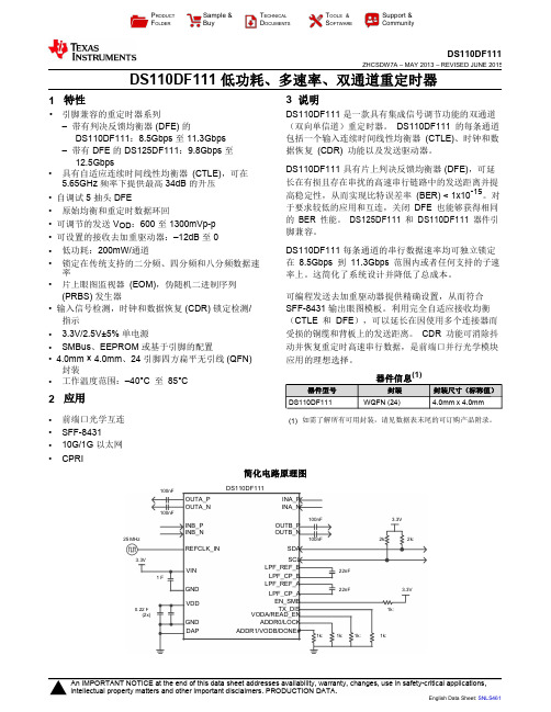
PRODUCT Sample&T ECHNICAL T OOLS&Support&F OLDER Buy D OCUMENTS S OFTWARE CommunityDS110DF111ZHCSDW7A–MAY2013–REVISED JUNE2015 DS110DF111低功耗、多速率、双通道重定时器1特性3说明•引脚兼容的重定时器系列DS110DF111是一款具有集成信号调节功能的双通道–带有判决反馈均衡器(DFE)的(双向单信道)重定时器。
DS110DF111的每条通道DS110DF111:8.5Gbps至11.3Gbps包括一个输入连续时间线性均衡器(CTLE)、时钟和数–带有DFE的DS125DF111:9.8Gbps至据恢复(CDR)功能以及发送驱动器。
12.5GbpsDS110DF111具有片上判决反馈均衡器(DFE),可延•具有自适应连续时间线性均衡器(CTLE),可在长在有损且存在串扰的高速串行链路中的发送距离并提5.65GHz频率下提供最高34dB的升压•自调试5抽头DFE高稳定性,从而实现比特误差率(BER)<1x10-15。
对于要求较低的应用和互连,关闭DFE也能够获得相同•原始均衡和重定时数据环回的BER性能。
DS125DF111和DS110DF111器件引•可调节的发送V OD:600至1300mVp-p脚兼容。
•可设置的接收去加重驱动器:–12dB至0•低功耗:200mW/通道DS110DF111每条通道的串行数据速率均可独立锁定•锁定在传统支持的二分频、四分频和八分频数据速在8.5Gbps到11.3Gbps范围内或者任何支持的子速率率上。
这简化了系统设计并降低了总成本。
•片上眼图监视器(EOM),伪随机二进制序列(PRBS)发生器可编程发送去加重驱动器提供精确设置,从而符合•输入信号检测,时钟和数据恢复(CDR)锁定检测/SFF-8431输出眼图模板。
DS30BA101-3.125Gbps差分缓冲器

DS30BA101 ZHCS811A–FEBRUARY2012–REVISED APRIL2013DS30BA1013.125Gbps差分缓冲器查询样品:DS30BA101特性•DC的数据速率达到3.125Gbps•支持标清(SD)和高清(HD)视频分辨率•功耗:典型值为165mW•工业温度范围:-40°C至+85°C应用范围•电缆延长•信号缓冲和重复•安全和监控典型应用说明DS30BA101是一款高速差分缓冲器,此缓冲器用于电缆驱动、信号缓冲和信号重复应用。
它的全差分信号路径确保了出色的信号完整性和抗扰度。
DS30BA101以高达 3.125Gbps的数据速率驱动差分和单端传输线路。
输出电压振幅可由电缆的一个单个外部电阻器调节,此电缆将应用驱动进入75Ω单端和100Ω差分模式阻抗。
DS30BA101由一个单个3.3V电源供电,功耗165mW (典型值)。
它运行在-40°C至+85°C的全工业温度范围内,并且采用4mm x4mm16引脚超薄型四方扁平无引线(WQFN)封装。
S eri ali ze r 150Mbps100:Differential Cable orto75:Coaxial Cable3.125GbpsDS30BA101DS30EA101Max Cable Loss~50dB@1.5GHzDeserializerPlease be aware that an important notice concerning availability,standard warranty,and use in critical applications of Texas Instruments semiconductor products and disclaimers thereto appears at the end of this data sheet.长期备有HD/3G-SDI高清视频IC-TI,ADI,ST等品牌IC万*先*生*Q*Q:1*8*6*6*5*8*3*9*2*4*1ADV7611/ADV7280/ADV7441/AD9889/GV7600/GV7601/GV7704/STDP4020/STDP6038/LMH0002/LMH0340/LMH0341/LMH0074/LMH1983/LM1881/LM2611/LM2662/LM2576/LM2587/LM3674/LM22670/LM226 72/LM22675/LM22676/LM49450/LMZ12003/LMZ12002/LMZ12010/LMZ10503/LMZ10505/LMZ30606/L MZ30602/LMZ22005/LMZ31710/FDC2114/TMDS251/DRV5033/RTL8201/FLI32626H/GS2971/GS2989/DS25CP104A/高清SDI-TI-ADI品牌IC选型Q*Q*群:566162116高清视频类工程师技术沟通及资料分享,纯技术交流,禁止一切广告连接图NCNC NC NC 16151413IN+112OUT+IN-2DS30BA10111OUT-V EE3(top view)10V EE RVO49VCC5678NC CCNC NCDAP =V EEV 外露裸片连接垫是用于这个器件的一个负电端子。
里氏硬度计异型支撑环
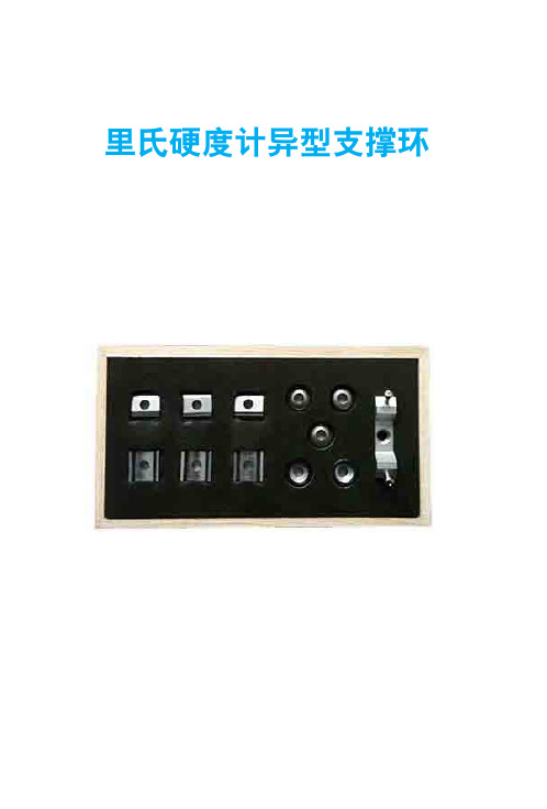
里氏硬度计异型支撑环序号代 号型 号异型支承环简图备 注103-03.7Z10-15测外圆柱面R10~R15203-03.8Z14.5-30测外圆柱面R14.5~R30303-03.9Z25-50测外圆柱面R25~R50403-03.10HZ11-13测内圆柱面R11~R13503-03.11HZ12.5-17测内圆柱面R12.5~R17603-03.12HZ16.5-30测内圆柱面R16.5~R30703-03.13K10-15测外球面SR10~SR15803-03.14K14.5-30测外球面SR14.5~SR30903-03.15HK11-13测内球面SR11~SR131003-03.16HK12.5-17测内球面SR12.5~SR171103-03.17HK16.5-30测内球面SR16.5~SR301203-03.18UN测外圆柱面,半径可调R10~∞沧州欧谱感谢以下网站对本资料的大力支持:测厚仪 超声波测厚仪钢板测厚仪 金属测厚仪管道测厚仪 钢管测厚仪厚度测量仪 超声测厚仪高温测厚仪 壁厚测量仪覆层测厚仪 膜厚仪涂层测厚仪 镀层测厚仪油漆测厚仪 漆膜测厚仪锌层测厚仪 防腐层测厚仪麦考特测厚仪 尼克斯测厚仪磁感应测厚仪 涡流测厚仪膜厚测试仪 覆层测厚仪 电镀层测厚仪 涂镀层测厚仪镀锌层测厚仪 电解测厚仪氧化膜测厚仪 磁性测厚仪干膜测厚仪 湿膜测厚仪镀铬测厚仪 超声波探伤仪超声波探伤仪 超声探伤仪数字超声波探伤仪 电火花检测仪焊缝探伤仪 超声波探伤仪金属探伤仪 便携式探伤仪钢结构探伤仪 磁粉探伤仪邵氏硬度计 橡胶硬度计便携式硬度计 便携式硬度计尼克斯测厚仪 里氏硬度计轧辊硬度计 巴氏硬度计韦氏硬度计 w-20韦氏硬度计模具硬度计 超声波硬度计洛氏硬度计 金属硬度计硬度测试仪 布氏硬度计肖氏硬度计 铸件硬度计轧辊硬度计 硬度仪钢板硬度计 铝合金硬度计电火花检测仪 电火花检漏仪电火花检测仪 漆膜划格器表面粗糙度仪 粗糙度测量仪粗糙度测试仪 喷砂粗糙度仪光洁度仪 便携式粗糙度仪粗糙度仪 附着力测试仪百格刀测试 百格刀 LED观片灯 黑白密度计光泽度仪 特价机票无损检测资源网 无损检测仪器无损123 网站目录标线测厚仪 硬度计超声波测厚仪 涂层测厚仪硬度计http://www.yingduji.top 无损检测http://www.wusunjiance.top探伤仪http://www.tanshangyi.top 硬度计测厚仪http://www.cehouyi.top 布氏硬度计洛氏硬度计 便携硬度计钢管硬度计 磷化膜测厚仪934-1巴氏硬度计 钢轨探伤仪lx-a邵氏硬度计 邵氏橡胶硬度计 涂层测厚仪 防腐层检测仪橡胶硬度计 工业观片灯油漆测厚仪 粗糙度检测仪。
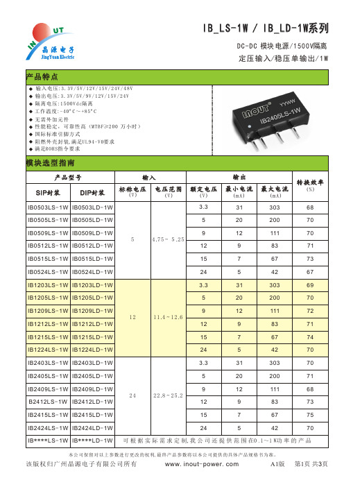
IB0505LS-1W.PDF
第2页 共3页
外观尺寸和引脚定义
19.6
9.5
IB****LS-1W
0.5
12
4
6
2.54
正视图
20.00
10.00 IB****LD-1W
正视图
6.0
印字面
12
0.90
4
6
0.50
4.10
0.50
建 议印 刷板 图:
0.30
12 4 6
侧视图
印字面 6.50
4.10 侧视图
底视图
15.24
1
7
7.62
14
11 9
0.50
5.08
底视图
俯 视 图,栅 格 间 距2 . 5 4 m m 开 孔 直 径1 . 0 0 m m
14
11 9
1
7
IB****LS-1W
引脚
1
2
4
6
定义 + Vin -Vin 0V + Vo
说明 输入正 输入负 输出地 输出
单 位 :mm
公差: 0.25
IB****LD-1W
引脚
A1版
第3页 共3页
1
7
9
11 14
定义 -Vin NC + Vo 0V + Vin
说明 输入负 无功能 输出正 输出地 输入正
基 本 应 用 电 路 推 荐:
+Vin -Vin
+Vin
C1
DC
-Vin
Vo
DC
C2
0V
LOAD
容 性 负 载 值 表:
输入电压
(VDC)
3.3或5
伊顿电子产品参考手册说明书

提供动力。
探索今天的伊顿。
我们提供:• 方案• • •动及动力总成解决方案马达控制设备命令和控制设备终端保护产品自动化和驱动产品134MOEM 市场综合样本目录2马达和线路控制设备伊顿拥有超过百年的接触器研发和制造经验,为用户提供至3185A 的线路控制解决方案,并提供不同系列的产品以满足用户的的多种要求Xstart 系列接触器:全球化的产品,提供包括UL 在内的主流认证,最高达3185安培(AC-1)的产品:• 独特的CT 型励磁机构,功耗更小;• 115A 以上集成电子线路板,降低功耗同时工作电压幅度更宽;• 580A 以上真空灭弧,应对严苛使用环境,业界最长预期寿命;• 提供本地化的XstartC 系列(认证情况请咨询当地销售办事处)。
D 系列接触器:本地化的产品,提供最高到500A 的高效控制和保护方案,应用于泵、风机、压缩机等场合,提供功能全面的辅助触点和宽幅的控制线圈电压选项。
• 齐全的线圈控制电压,185A 以上更提供交直流通用产品;• 全系列内置辅助触点• 百万次以上电气寿命• 使用温度-20 °C ~ +55 °CE 系列接触器:全球最小的电磁接触器之一,有效地利用空间,可靠性增强,材料使用更高效。
E 系列接触器额定值可至AC-3, 95A@400V ,最高工作电压高达660V ,体积小巧,却提供强大的性能。
• 百万次以上电气寿命• 690V 绝缘额定值• 最多可加装6个辅助触点模块• 常用交流控制电压及直流24VDC 线圈1马达控制设备目录电机控制产品 xStart C 接触器式继电器DILA..C 接触器DILM..C 过载继电器ZB..C电动机保护断路器PKZMC 电机控制产品 D 系列接触器 XTCD 热过载继电器 XTOD 电气行业解决方案 Eline 控制继电器 XTRG 接触器 XTCG热过载继电器 XTOD/XTOG电机控制产品 xStart C电机控制产品 D 系列电气行业解决方案Eline1接触器式继电器DILA..C目录系统概览 . . . . . . . . . . . . . . . . . . . . . . . . . . . . . . . . . . . . . . . . . . . . . . . . . . . . . . . . . . . . . . . . . . . . .本体DILA..C . . . . . . . . . . . . . . . . . . . . . . . . . . . . . . . . . . . . . . . . . . . . . . . . . . . . . . . . . . . . . . . . . .辅助触点模块 . . . . . . . . . . . . . . . . . . . . . . . . . . . . . . . . . . . . . . . . . . . . . . . . . . . . . . . . . . . . . . . .附件 . . . . . . . . . . . . . . . . . . . . . . . . . . . . . . . . . . . . . . . . . . . . . . . . . . . . . . . . . . . . . . . . . . . . . . . . .操作电压 . . . . . . . . . . . . . . . . . . . . . . . . . . . . . . . . . . . . . . . . . . . . . . . . . . . . . . . . . . . . . . . . . . . . .特性曲线,触点行程图 . . . . . . . . . . . . . . . . . . . . . . . . . . . . . . . . . . . . . . . . . . . . . . . . . . . . . . . .技术数据 . . . . . . . . . . . . . . . . . . . . . . . . . . . . . . . . . . . . . . . . . . . . . . . . . . . . . . . . . . . . . . . . . . . . .尺寸 . . . . . . . . . . . . . . . . . . . . . . . . . . . . . . . . . . . . . . . . . . . . . . . . . . . . . . . . . . . . . . . . . . . . . . . . .4极触点多种组合约定发热电流(I th )16A 交流与直流操作的产品尺寸相同直流操作的产品内置浪涌抑制器••••接触器式继电器DILA..C35791112131911接触器式继电器DILA..C说明121接触器式继电器DILA..C系统概览31接触器式继电器DILA..C系统概览4系统概览本体AC 或DC 操作电磁系统AC DC 可以扩展到8对触点反向互锁触点模块化系统螺钉连接和卡装手指接触防护螺钉端子第5页起抑制电路用于直流操作接触器式继电器的保护电路(所有直流型均内置)用于交流操作接触器式继电器的保护电路第32页起辅助触点模块23, 42或4极反向互锁触点第7页起124 – 400V, 50, 60, 50/60 Hz0.8 – 1.1 × U c 24 VA/3.4 VA 24 – 220 V DC0.8 – 1.1 × U c 于24 V :0.7 – 1.3 × U c 无附加辅助触点模块环境温度+40°C 3W/3W1接触器式继电器DILA..C本体5接线方式:螺钉端子触点N/O = 常开N/C = 常闭带反向互锁触点的本体额定工作电流AC – 15220 V230 V240 VI e约定发热电流,敞开,于60°CI th代码序号触点序号380 V400 V415 VI e1本体DILAC-XHI(V)...DILAC-XHI(V)...DILAC-XHI(V)...DILA-40C(220-230V50Hz)114842DILA-31C(220-230V50Hz)114852DILA-22C(220-230V50Hz)114862DILA-40C(24VDC)114847DILA-31C(24VDC)114857DILA-22C(24VDC)1148671件1件1件可以组合辅助触点模块标准包装说明AC 操作型号订货号操作电压220-230V50HzDC 操作型号订货号操作电压24VDC附件1 抑制器2 辅助触点模块操作电压页数32711触点编号,符合EN 50011线圈端子标记,符合EN 50005直流操作的接触器式继电器具有一个内置的保护电路。
LMZ10501和LMZ10500SIMPLE SWITCHER nano 模块评估板用户指南说明书
User's GuideSNVA491B–August2011–Revised April2013 AN-2166LMZ10501and LMZ10500SIMPLE SWITCHER®Nano Module Evaluation Board1IntroductionThe LMZ10501and LMZ10500SIMPLE SWITCHER nano modules are easy-to-use DC-DC solutionsoptimized for space-constrained applications.The LMZ10501is capable of driving up to1A load withexcellent power conversion efficiency,line and load regulation,and EMI performance.The LMZ10500is a 650mA version module and is pin-to-pin compatible with the LMZ10501.The LMZ10501and LMZ10500Evaluation Board is configured for1.8V output voltage from2.7V to5.5Vinput.The resistor voltage divider RT and RBset the output voltage.The external capacitor CVCbypassesthe VCON pin and provides additional soft start time.for component selection and device informationdetails,see the device-specific data sheet.The board features additional component footprints for various device enabling schemes and AC signal injection terminals for feedback loop measurements.The evaluation board with its default Bill of Materials offers great EMI performance,complying with the EN 55022Class B radiated emissions standard.2Board Specifications•VIN=2.7V to5.5V•VOUT=1.8V(default setting)•1A max load(LMZ10501)•650mA max load(LMZ10500)•2MHz switching frequency•4layers PCB with1oz copper• 4.3x4.3cm(1700x1700mil)PCB size•Low radiated EMI(EN55022Class B compliant)SIMPLE SWITCHER is a registered trademark of Texas Instruments.All other trademarks are the property of their respective owners.1 SNVA491B–August2011–Revised April2013AN-2166LMZ10501and LMZ10500SIMPLE SWITCHER®Nano ModuleEvaluation Board Submit Documentation FeedbackCopyright©2011–2013,Texas Instruments IncorporatedTypical Performance Characteristics 3Typical Performance CharacteristicsOutput RippleRadiated EMI2AN-2166LMZ10501and LMZ10500SIMPLE SWITCHER ®Nano Module SNVA491B–August 2011–Revised April 2013Evaluation BoardSubmit Documentation FeedbackCopyright ©2011–2013,Texas Instruments IncorporatedOPTIONAL COMPONENT FOR AC INJECTION FOR CONTROL LOOP MEASUREMENTSBOARD EDGE PAD ASSIGNMENTS FOR QUICK CONNECTIONOPTIONALPLACE CIN AS CLOSE AS POSSIBLE TO THE PVIN AND PGND PINS FOR GOOD BYPASSRESISTORS RT AND RB SET THE OUTPUTVOLTAGEPLACE C VC AS CLOSE AS POSSIBLE TO THE VCONAND SGND PINSENABLE OPTComponents marked with (*) are notpopulated on the board Evaluation Board Schematic and Bill of Materials4Evaluation Board Schematic and Bill of MaterialsFigure 1.Evaluation Board SchematicTable 1.LMZ10501and LMZ10500Bill of Materials,V IN =2.7V to 5.5V,V OUT =1.8V,I OUT (MAX)=1000mA /650mADesignatorDescription Case Size Manufacturer Manufacturer P/N QuantityU1SIMPLE SWITCHERSE08A Texas InstrumentsLMZ10501SE or 1Nano Module LMZ10500SE C IN ,C OUT10µF,X5R,10V0805KEMET C0805C106K8PACTU 2C VC 1000pF 0603TDK C1608C0G2A102J 1R B 82.5k Ω0603Vishay-Dale CRCW060382K5FKEA 1R T 187k Ω0603Vishay-Dale CRCW0603187KFKEA 1R EN1k Ω0603Vishay-Dale CRCW06031K00FKEA 1(optional)R INJ10Ω0603Vishay-DaleCRCW060310R0FKEA1(optional)3SNVA491B–August 2011–Revised April 2013AN-2166LMZ10501and LMZ10500SIMPLE SWITCHER ®Nano ModuleEvaluation BoardSubmit Documentation FeedbackCopyright ©2011–2013,Texas Instruments IncorporatedEvaluation Board Layout 4.1Optional Components and Footprints•RINJ resistor–allows for a network analyzer connection to measure the control loop response.Replacethis resistor with a short in a final design if control loop measurements are not needed.•RPU resistor–an optional footprint to pull EN up to VINwith an external resistor.EN is internally pulledup to VINby a790kΩresistor.•REN–an optional resistor in series with the EN pin.•RPD –an optional pull-down resistor for the QENgate.•QEN–an optional footprint to use an N-ch MOSFET as a pull-down device for EN.•J1–jumper to select how to drive EN.Connecting the jumper pins1and2allows for driving ENdirectly from the EN turret at the edge of the board.Connecting the jumper pins2and3allows fordriving the gate of the pull-down device QEN.•EC1–board edge connector for quick testing.•COUT footprints–the solder mask on the VOUTside of the board is removed to allow for different outputcapacitor configurations.5Evaluation Board LayoutFigure2.Evaluation Board Top View4AN-2166LMZ10501and LMZ10500SIMPLE SWITCHER®Nano Module SNVA491B–August2011–Revised April2013 Evaluation Board Submit Documentation FeedbackCopyright©2011–2013,Texas Instruments Incorporated Evaluation Board LayoutFigure3.Evaluation Board Bottom ViewFigure4.Evaluation Board Assembly(DNP=not populated components)5 SNVA491B–August2011–Revised April2013AN-2166LMZ10501and LMZ10500SIMPLE SWITCHER®Nano ModuleEvaluation Board Submit Documentation FeedbackCopyright©2011–2013,Texas Instruments Incorporated30 mV/Div250 MHz BW500 µs/DivCOUT = 10 F 10V 0805 X5RLOAD CURRENTOUTPUT VOLTAGE500 mA/Div 10 mV/Div500 MHz BW1 µs/DivCOUT = 10 F 10V 0805 X5RVOUT RIPPLETypical Performance for V OUT =1.8V6Typical Performance for V OUT =1.8VUnless otherwise specified the following conditions apply:V IN =5V,I OUT =1A,T A =25°C6AN-2166LMZ10501and LMZ10500SIMPLE SWITCHER ®Nano Module SNVA491B–August 2011–Revised April 2013Evaluation BoardSubmit Documentation FeedbackCopyright ©2011–2013,Texas Instruments IncorporatedCf = 0603YD105MAT AVXLf = VLS252015T-1R0N1R7 TDKTypical Performance for V OUT =1.8VInput LC Filter for Conducted EMI 7SNVA491B–August 2011–Revised April 2013AN-2166LMZ10501and LMZ10500SIMPLE SWITCHER ®Nano ModuleEvaluation BoardSubmit Documentation FeedbackCopyright ©2011–2013,Texas Instruments IncorporatedTypical Performance for V OUT =1.8V8AN-2166LMZ10501and LMZ10500SIMPLE SWITCHER ®Nano Module SNVA491B–August 2011–Revised April 2013Evaluation BoardSubmit Documentation FeedbackCopyright ©2011–2013,Texas Instruments Incorporated Other Output Voltage Settings7Other Output Voltage SettingsFigure 5.V OUT =1.2VFigure 6.V OUT =2.5VFigure 7.V OUT =3.3VFor other output voltages,choose R T =80k Ωto 300k ΩThen calculate R B usingR B =V OUT x R T /(5.875V –V OUT )(1)9SNVA491B–August 2011–Revised April 2013AN-2166LMZ10501and LMZ10500SIMPLE SWITCHER ®Nano ModuleEvaluation BoardSubmit Documentation FeedbackCopyright ©2011–2013,Texas Instruments IncorporatedIMPORTANT NOTICETexas Instruments Incorporated and its subsidiaries(TI)reserve the right to make corrections,enhancements,improvements and other changes to its semiconductor products and services per JESD46,latest issue,and to discontinue any product or service per JESD48,latest issue.Buyers should obtain the latest relevant information before placing orders and should verify that such information is current and complete.All semiconductor products(also referred to herein as“components”)are sold subject to TI’s terms and conditions of sale supplied at the time of order acknowledgment.TI warrants performance of its components to the specifications applicable at the time of sale,in accordance with the warranty in TI’s terms and conditions of sale of semiconductor products.Testing and other quality control techniques are used to the extent TI deems necessary to support this warranty.Except where mandated by applicable law,testing of all parameters of each component is not necessarily performed.TI assumes no liability for applications assistance or the design of Buyers’products.Buyers are responsible for their products and applications using TI components.To minimize the risks associated with Buyers’products and applications,Buyers should provide adequate design and operating safeguards.TI does not warrant or represent that any license,either express or implied,is granted under any patent right,copyright,mask work right,or other intellectual property right relating to any combination,machine,or process in which TI components or services are rmation published by TI regarding third-party products or services does not constitute a license to use such products or services or a warranty or endorsement e of such information may require a license from a third party under the patents or other intellectual property of the third party,or a license from TI under the patents or other intellectual property of TI.Reproduction of significant portions of TI information in TI data books or data sheets is permissible only if reproduction is without alteration and is accompanied by all associated warranties,conditions,limitations,and notices.TI is not responsible or liable for such altered rmation of third parties may be subject to additional restrictions.Resale of TI components or services with statements different from or beyond the parameters stated by TI for that component or service voids all express and any implied warranties for the associated TI component or service and is an unfair and deceptive business practice. TI is not responsible or liable for any such statements.Buyer acknowledges and agrees that it is solely responsible for compliance with all legal,regulatory and safety-related requirements concerning its products,and any use of TI components in its applications,notwithstanding any applications-related information or support that may be provided by TI.Buyer represents and agrees that it has all the necessary expertise to create and implement safeguards which anticipate dangerous consequences of failures,monitor failures and their consequences,lessen the likelihood of failures that might cause harm and take appropriate remedial actions.Buyer will fully indemnify TI and its representatives against any damages arising out of the use of any TI components in safety-critical applications.In some cases,TI components may be promoted specifically to facilitate safety-related applications.With such components,TI’s goal is to help enable customers to design and create their own end-product solutions that meet applicable functional safety standards and requirements.Nonetheless,such components are subject to these terms.No TI components are authorized for use in FDA Class III(or similar life-critical medical equipment)unless authorized officers of the parties have executed a special agreement specifically governing such use.Only those TI components which TI has specifically designated as military grade or“enhanced plastic”are designed and intended for use in military/aerospace applications or environments.Buyer acknowledges and agrees that any military or aerospace use of TI components which have not been so designated is solely at the Buyer's risk,and that Buyer is solely responsible for compliance with all legal and regulatory requirements in connection with such use.TI has specifically designated certain components as meeting ISO/TS16949requirements,mainly for automotive use.In any case of use of non-designated products,TI will not be responsible for any failure to meet ISO/TS16949.Products ApplicationsAudio /audio Automotive and Transportation /automotiveAmplifiers Communications and Telecom /communicationsData Converters Computers and Peripherals /computersDLP®Products Consumer Electronics /consumer-appsDSP Energy and Lighting /energyClocks and Timers /clocks Industrial /industrialInterface Medical /medicalLogic Security /securityPower Mgmt Space,Avionics and Defense /space-avionics-defense Microcontrollers Video and Imaging /videoRFID OMAP Applications Processors /omap TI E2E Community Wireless Connectivity /wirelessconnectivityMailing Address:Texas Instruments,Post Office Box655303,Dallas,Texas75265Copyright©2013,Texas Instruments Incorporated。
LMZ10505EXT:5A SIMPLE SWITCHER电源方案

LMZ10505EXT:5A SIMPLE SWITCHER电源方案佚名【期刊名称】《世界电子元器件》【年(卷),期】2010(000)011【摘要】@@ NS公司的LMZ10505EXT是5A SIMPLE SWITCHER电源模块,最大输入电压5.5V,符合军用标准.LMZ10505EXT电源模块的最大输出功率为25W,输出电流高达5A,它的输入电压2.95V至5.5V,输出电压0.8V~5V,效率高达96%,LMZ10505EXT电源模块主要用在点负载转换,空间受限的应用,极端温度/无空气对流的环境以及对噪音敏感如传感器,医疗设备等.【总页数】2页(P18-19)【正文语种】中文【相关文献】1.全新的SIMPLE SWITCHER易电源电源模块 [J],2.SIMPLE SWITCHER易电源产品系列及电源模块 [J], NS公司3.TI LMR33630SIMPLE SWITCHER高效稳压器解决方案 [J],4.Development of simple HPLC/UV with a column-switching method for the determination of nicotine and cotinine in hair samples [J], Masayoshi Tsuji;Yayoi Mori;Hideyuki Kanda;Teruna Ito;Tomoo Hidaka;Takeyasu Kakamu;Tomohiro Kumagai;Takehito Hayakawa;Yoneatsu Osaki;Tetsuhito Fukushima5.TI推出最高效率的SIMPLE SWITCHER同步转换器 [J],因版权原因,仅展示原文概要,查看原文内容请购买。
- 1、下载文档前请自行甄别文档内容的完整性,平台不提供额外的编辑、内容补充、找答案等附加服务。
- 2、"仅部分预览"的文档,不可在线预览部分如存在完整性等问题,可反馈申请退款(可完整预览的文档不适用该条件!)。
- 3、如文档侵犯您的权益,请联系客服反馈,我们会尽快为您处理(人工客服工作时间:9:00-18:30)。
LMZ10505 SNVS633G–JANUARY2010–REVISED APRIL2013 LMZ105055A SIMPLE SWITCHER®Power Module with5.5V Maximum Input VoltageCheck for Samples:LMZ10505FEATURESELECTRICAL SPECIFICATIONS •Integrated Shielded Inductor•25W Maximum Total Output Power•Flexible Startup Sequencing Using External•Up to5A Output Current Soft-Start,Tracking,and Precision Enable•Input Voltage Range2.95V to5.5V •Protection Against In-Rush Currents and•Output Voltage Range0.8V to5V Faults such as Input UVLO and Output Short-Circuit•±1.63%Feedback Voltage Accuracy OverTemperature•-40°C to+125°C Junction TemperatureOperating Range•Efficiency up to96%•Single Exposed Pad and Standard Pinout forPERFORMANCE BENEFITS Easy Mounting and Manufacturing•Pin-to-Pin Compatible with•Operates at High Ambient Temperatures –LMZ10503(3A/15W max)•High Efficiency up to96%Reduces SystemHeat Generation–LMZ10504(4A/20W max)•Low Radiated Emissions(EMI)Complies with •Fully Enable for WEBENCH®and PowerEN55022Class B Standard(2) Designer•Passes10V/m Radiated Immunity EMI Ttest APPLICATIONS Standard EN610004-3•Low Output Voltage Ripple of10mV Allows •Point-of-Load Conversions from3.3V and5Vfor Powering Noise-Sensitive Transceiver and RailsSignaling ICs•Space constrained applications•Fast Transient Response for Powering FPGAs •Extreme Temperatures/no Air Flowand ASICsEnvironments•Noise Sensitive Applications(i.e.Transceiver,DESCRIPTIONMedical)The LMZ10505SIMPLE SWITCHER®power moduleis a complete,easy-to-use DC-DC solution capable ofdriving up to a5A load with exceptional powerconversion efficiency,output voltage accuracy,lineand load regulation.The LMZ10505is available in aninnovative package that enhances thermalperformance and allows for hand or machinesoldering.Figure1.Easy to Use7Pin PackagePFM7Pin Package10.16x13.77x4.57mm(0.4x0.39x0.18in)θJA=20°C/W,θJC=1.9°C/W(1)RoHS Compliant(1)θJA measured on a2.25”x2.25”(5.8cm x5.8cm)four layerboard,with one ounce copper,thirty six10mil thermal vias,noair flow,and1W power dissipation.Refer to PCB LayoutDiagrams or Evaluation Board Application Note:AN-2022(2)EN55022:2006,+A1:2007,FCC Part15Subpart B:2007.(SNVA421).See Table9and layout for information on device under test.Please be aware that an important notice concerning availability,standard warranty,and use in critical applications ofTexas Instruments semiconductor products and disclaimers thereto appears at the end of this data sheet.All trademarks are the property of their respective owners.PRODUCTION DATA information is current as of publication date.Copyright©2010–2013,Texas Instruments Incorporated Products conform to specifications per the terms of the TexasInstruments standard warranty.Production processing does notnecessarily include testing of all parameters.LMZ10505SNVS633G–JANUARY2010–REVISED DESCRIPTION(CONTINUED)The LMZ10505can accept an input voltage rail between2.95V and5.5V and deliver an adjustable and highly accurate output voltage as low as0.8V.One megahertz fixed frequency PWM switching provides a predictable EMI characteristic.Two external compensation components can be adjusted to set the fastest response time,while allowing the option to use ceramic and/or electrolytic output capacitors.Externally programmable soft-start capacitor facilitates controlled startup.The LMZ10505is a reliable and robust solution with the following features:lossless cycle-by-cycle peak current limit to protect for over current or short-circuit fault,thermal shutdown,input under-voltage lock-out,and pre-biased startup.System PerformanceFigure2.Current Derating(V OUT=3.3V)Figure3.Efficiency(V OUT=3.3V)Figure4.Radiated Emissions(EN55022,Class B)2Submit Documentation Feedback Copyright©2010–2013,Texas Instruments IncorporatedProduct Folder Links:LMZ10505LMZ10505SNVS633G –JANUARY 2010–REVISED APRIL 2013Typical Application CircuitConnection DiagramFigure 5.7-Lead PFM -Top View Package Number NDW0007APIN DESCRIPTIONSPin NumberName Description1VIN Power supply input.A low ESR input capacitance should be located as close as possible to the VIN pin and exposed pad (EP).2EN Active high enable input for the device.3SSSoft-start control pin.An internal 2µA current source charges an external capacitor connected between SS and GND pins to set the output voltage ramp rate during startup.The SS pin can also be used to configure the tracking feature.4GND Power ground and signal ground.Provide a direct connection to the EP.Place the bottom feedback resistor as close as possible to GND and FB pin.5FB Feedback pin.This is the inverting input of the error amplifier used for sensing the output voltage.Keep the copper area of this node small.6,7VOUT The output terminal of the internal inductor.Connect the output filter capacitor between VOUT pin and EP.EPExposed Exposed pad is used as a thermal connection to remove heat from the device.Connect this pad to the PC Padboard ground plane in order to reduce thermal resistance value.EP must also provide a direct electrical connection to the input and output capacitors ground terminals.Connect EP to pin 4.These devices have limited built-in ESD protection.The leads should be shorted together or the device placed in conductive foam during storage or handling to prevent electrostatic damage to the MOS gates.Copyright ©2010–2013,Texas Instruments Incorporated Submit Documentation Feedback3Product Folder Links:LMZ10505LMZ10505SNVS633G–JANUARY2010–REVISED Absolute Maximum Ratings(1)(2)VIN,VOUT,EN,FB,SS to GND-0.3V to6.0V ESD Susceptibility(3)±2kV Power Dissipation Internally Limited Junction Temperature150°C Storage Temperature Range-65°C to150°C Peak Reflow Case Temperature245°C (30sec)For soldering specifications,refer to the following document:/lit/snoa549c(1)Absolute Maximum Ratings are limits beyond which damage to the device may occur.Operating Ratings are conditions under whichoperation of the device is intended to be functional.For ensured specifications and test conditions,see the Electrical Characteristics. (2)If Military/Aerospace specified devices are required,please contact the Texas Instruments Sales Office/Distributors for availability andspecifications.(3)The human body model is a100pF capacitor discharged through a1.5kΩresistor into each pin.Test method is per JESD22-AI14S.Operating Ratings(1)VIN to GND 2.95V to5.5V Junction Temperature(T J)-40°C to125°C (1)Absolute Maximum Ratings are limits beyond which damage to the device may occur.Operating Ratings are conditions under whichoperation of the device is intended to be functional.For ensured specifications and test conditions,see the Electrical Characteristics.Electrical CharacteristicsSpecifications with standard typeface are for T J=25°C only;limits in bold face type apply over the operating junction temperature range T J of-40°C to125°C.Minimum and maximum limits are ensured through test,design,or statistical correlation.Typical values represent the most likely parametric norm at T J=25°C,and are provided for reference purposes only.V IN=V EN=3.3V,unless otherwise indicated in the conditions column.Symbol Parameter Conditions Min(1)Typ(2)Max(1)Units SYSTEM PARAMETERSV FB Total Feedback Voltage Variation V IN=2.95V to5.5V0.780.80.82V Including Line and Load Regulation V OUT=2.5VI OUT=0A to5AV FB Feedback Voltage Variation V IN=3.3V,V OUT=2.5V0.7870.80.812VI OUT=0AV FB Feedback Voltage Variation V IN=3.3V,V OUT=2.5V0.7850.7980.81VI OUT=5AV IN(UVLO)Input UVLO Threshold(Measured at VIN Rising 2.6 2.95V pin)Falling 1.95 2.4I SS Soft-Start Current Charging Current2µAI Q Non-Switching Input Current V FB=1V 1.553mAI SD Shut Down Quiescent Current V IN=5.5V,V EN=0V267500µAI OCL Output Current Limit(Average Current)V OUT=2.5V 5.17.38.7Af FB Frequency Fold-back In current limit250kHz PWM SECTIONf SW Switching Frequency75010001160kHzD range PWM Duty Cycle Range0100% ENABLE CONTROLV EN-IH EN Pin Rising Threshold 1.23 1.8V V EN-IF EN Pin Falling Threshold0.8 1.06V (1)Min and Max limits are100%production tested at an ambient temperature(T A)of25°C.Limits over the operating temperature range areensured through correlation using Statistical Quality Control(SQC)methods.Limits are used to calculate Average Outgoing Quality Level(AOQL).(2)Typical numbers are at25°C and represent the most likely parametric norm.4Submit Documentation Feedback Copyright©2010–2013,Texas Instruments IncorporatedProduct Folder Links:LMZ10505LMZ10505 SNVS633G–JANUARY2010–REVISED APRIL2013Electrical Characteristics(continued)Specifications with standard typeface are for T J=25°C only;limits in bold face type apply over the operating junction temperature range T J of-40°C to125°C.Minimum and maximum limits are ensured through test,design,or statistical correlation.Typical values represent the most likely parametric norm at T J=25°C,and are provided for reference purposes only.V IN=V EN=3.3V,unless otherwise indicated in the conditions column.Symbol Parameter Conditions Min(1)Typ(2)Max(1)Units THERMAL CONTROLT SD T J for Thermal Shutdown145°C T SD-HYS Hysteresis for Thermal Shutdown10°C THERMAL RESISTANCEθJA Junction to Ambient See(3)20°C/W θJC Junction to Case No air flow 1.9°C/W PERFORMANCE PARAMETERSΔV OUT Output Voltage Ripple Refer to Table310mV pk-V OUT=2.5V pkBandwidth Limit=2MHzΔV OUT Output Voltage Ripple Refer to Table55mV pk-Bandwidth Limit=20MHz pk ΔV FB/V FB Feedback Voltage Line RegulationΔV IN=2.95V to5.5V0.04%I OUT=0AΔV OUT/V OUT Output Voltage Line RegulationΔV IN=2.95V to5.5V0.04%I OUT=0A,V OUT=2.5VΔV FB/V FB Feedback Voltage Load Regulation I OUT=0A to5A0.25%ΔV OUT/V OUT Output Voltage Load Regulation I OUT=0A to5A0.25%V OUT=2.5VEfficiencyηPeak Efficiency(1A)V IN=5V V OUT=3.3V96.1V OUT=2.5V94.8V OUT=1.8V93.1%V OUT=1.5V92V OUT=1.2V90.4V OUT=0.8V86.8ηPeak Efficiency(1A)V IN=3.3V V OUT=2.5V95.7%V OUT=1.8V94.1V OUT=1.5V93.0V OUT=1.2V91.6V OUT=0.8V88.3ηFull Load Efficiency(3A)V IN=5V V OUT=3.3V93.1%V OUT=2.5V91.2V OUT=1.8V88.5V OUT=1.5V86.7V OUT=1.2V84.1V OUT=0.8V78.2ηFull Load Efficiency(3A)V IN=3.3V V OUT=2.5V89.8%V OUT=1.8V86.9V OUT=1.5V85.1V OUT=1.2V82.5V OUT=0.8V76.2(3)θJA measured on a2.25”x2.25”(5.8cm x5.8cm)four layer board,with one ounce copper,thirty six10mil thermal vias,no air flow,and1W power dissipation.Refer to PCB Layout Diagrams or Evaluation Board Application Note:AN-2022(SNVA421).Copyright©2010–2013,Texas Instruments Incorporated Submit Documentation Feedback5Product Folder Links:LMZ10505LMZ10505SNVS633G–JANUARY2010–REVISED Typical Performance CharacteristicsUnless otherwise specified,the following conditions apply:V IN=V EN=5.0V,C IN is47µF10V X5R ceramic capacitor;T AMBIENT=25°C for efficiency curves and waveforms.Load Transient Response Load Transient Response V IN=3.3V,V OUT=2.5V,I OUT=0.5A to4.5A to0.5A step V IN=5.0V,V OUT=2.5V,I OUT=0.5A to4.5A to0.5A step 20MHz Bandwidth Limited20MHz Bandwidth Limited Refer to Table5for BOM,includes optional components Refer to Table5for BOM,includes optional componentsFigure6.Figure7.Output Voltage Ripple Output Voltage Ripple V IN=3.3V,V OUT=2.5V,I OUT=5A,20mV/DIV V IN=5.0V,V OUT=2.5V,I OUT=5A,20mV/DIV Refer to Table5for BOM Refer to Table5for BOMFigure8.Figure9.Efficiency EfficiencyV OUT=3.3V V OUT=2.5VFigure10.Figure11.6Submit Documentation Feedback Copyright©2010–2013,Texas Instruments IncorporatedProduct Folder Links:LMZ10505LMZ10505 SNVS633G–JANUARY2010–REVISED APRIL2013Typical Performance Characteristics(continued)Unless otherwise specified,the following conditions apply:V IN=V EN=5.0V,C IN is47µF10V X5R ceramic capacitor;T AMBIENT =25°C for efficiency curves and waveforms.Efficiency EfficiencyV OUT=1.8V V OUT=1.5VFigure12.Figure13.Efficiency EfficiencyV OUT=1.2V V OUT=0.8VFigure14.Figure15.Current Derating Current DeratingV IN=5V,θJA=20°C/W V IN=3.3V,θJA=20°C/WFigure16.Figure17.Copyright©2010–2013,Texas Instruments Incorporated Submit Documentation Feedback7Product Folder Links:LMZ10505LMZ10505SNVS633G–JANUARY2010–REVISED Typical Performance Characteristics(continued)Unless otherwise specified,the following conditions apply:V IN=V EN=5.0V,C IN is47µF10V X5R ceramic capacitor;T AMBIENT =25°C for efficiency curves and waveforms.Radiated Emissions(EN55022,Class B)V IN=5V,V OUT=2.5V,I OUT=5A StartupEvaluation Board V OUT=2.5V,I OUT=0AFigure18.Figure19.Pre-biased StartupV OUT=2.5V,I OUT=0AFigure20.8Submit Documentation Feedback Copyright©2010–2013,Texas Instruments IncorporatedProduct Folder Links:LMZ10505C in8I OUT xD x (1 - D)f SW x 'VINLMZ10505 SNVS633G–JANUARY2010–REVISED APRIL2013Block DiagramDESIGN GUIDELINE AND OPERATING DESCRIPTIONDesign StepsLMZ10505is fully supported by Webench®and offers the following:component selection,performance, electrical,and thermal simulations as well as the Build-It board,for a reduced design time.On the other hand,all external components can be calculated by following the design procedure below.1.Determine the input voltage and output voltage.Also,make note of the ripple voltage and voltage transientrequirements.2.Determine the necessary input and output capacitance.3.Calculate the feedback resistor divider.4.Select the optimized compensation component values.5.Estimate the power dissipation and board thermal requirements.6.Follow the PCB design guideline.7.Learn about the LMZ10505features such as enable,input UVLO,soft-start,tracking,pre-biased startup,current limit,and thermal shutdown.Design ExampleFor this example the following application parameters exist.•V IN=5V•V OUT=2.5V•I OUT=5A•ΔV OUT=20mV pk-pk•ΔV o_tran=±20mV pk-pkInput Capacitor SelectionA22µF or47µF high quality dielectric(X5R,X7R)ceramic capacitor rated at twice the maximum input voltage is typically sufficient.The input capacitor must be placed as close as possible to the VIN pin and GND exposed pad to substantially eliminate the parasitic effects of any stray inductance or resistance on the PC board and supply lines.Neglecting capacitor equivalent series resistance(ESR),the resultant input capacitor AC ripple voltage is a triangular waveform.The minimum input capacitance for a given peak-to-peak value(ΔV IN)of V IN is specified as follows:(1) Copyright©2010–2013,Texas Instruments Incorporated Submit Documentation Feedback9Product Folder Links:LMZ10505I step x V FB x L x V IN4 x V OUT x (V IN -V OUT ) x 'Vo_tranC ot'i L =(5V ± 2.5V) x 1.5 P H x 1 MHz2.5V 5V= 833 mA'i L =(V IN - V OUT ) x DL x f SW'C OUT ='i L8 x f SW x ['V OUT ± ('i L x R ESR )]I Cin(RMS) = I OUT x D(1-D)C in 85A x ( ) x (1 - )1 MHz x 50 mV2.5V 5V2.5V 5V 8 25 µF D =V OUT V INLMZ10505SNVS633G –JANUARY 2010–REVISED APRIL 2013where the PWM duty cycle,D,is given by:(2)If ΔV IN is 1%of V IN ,this equals to 50mV and f SW =1MHz(3)A second criteria before finalizing the C in bypass capacitor is the RMS current capability.The necessary RMS current rating of the input capacitor to a buck regulator can be estimated by(4)(5)With this high AC current present in the input capacitor,the RMS current rating becomes an important parameter.The maximum input capacitor ripple voltage and RMS current occur at 50%duty cycle.Select an input capacitor rated for at least the maximum calculated I Cin(RMS).Additional bulk capacitance with higher ESR may be required to damp any resonance effects of the input capacitance and parasitic inductance.Output Capacitor SelectionIn general,22µF to 100µF high quality dielectric (X5R,X7R)ceramic capacitor rated at twice the maximum output voltage is sufficient given the optimal high frequency characteristics and low ESR of ceramic dielectrics.Although,the output capacitor can also be of electrolytic chemistry for increased capacitance density.Two output capacitance equations are required to determine the minimum output capacitance.One equation determines the output capacitance (C O )based on PWM ripple voltage.The second equation determines C O based on the load transient characteristics.Select the largest capacitance value of the two.The minimum capacitance,given the maximum output voltage ripple (ΔV OUT )requirement,is determined by the following equation:(6)Where the peak to peak inductor current ripple (Δi L )is equal to:(7)R ESR is the total output capacitor ESR,L is the inductance value of the internal power inductor,where L =1.5µH,and f SW =1MHz.Therefore,per the design example:(8)The minimum output capacitance requirement due to the PWM ripple voltage is:(9)(10)Three miliohms is a typical R ESR value for ceramic capacitors.The following equation provides a good first pass capacitance requirement for a load transient:(11)Where I step is the peak to peak load step (10%to 90%of the maximum load for this example),V FB =0.8V,and ΔV o_tran is the maximum output voltage deviation,which is ±20mV.Therefore the capacitance requirement for the given design parameters is:10Submit Documentation FeedbackCopyright ©2010–2013,Texas Instruments IncorporatedProduct Folder Links:LMZ10505V OUT = 0.8V x R fbt + R fbbRfbb (12)(13)In this particular design the output capacitance is determined by the load transient requirements.Table1lists some examples of commercially available capacitors that can be used with the LMZ10505.Table1.Recommended Output Filter CapacitorsC O(µF)Voltage(V),R ESR(mΩ)Make Manufacturer Part Number Case Size22 6.3,<5Ceramic,X5R TDK C3216X5R0J226M120647 6.3,<5Ceramic,X5R TDK C3216X5R0J476M120647 6.3,<5Ceramic,X5R TDK C3225X5R0J476M12104710.0,<5Ceramic,X5R TDK C3225X5R1A476M1210100 6.3,<5Ceramic,X5R TDK C3225X5R0J107M1210100 6.3,50Tantalum AVX TPSD157M006#0050D,7.5x4.3x2.9mm 100 6.3,25Organic Polymer Sanyo6TPE100MPB2B2,3.5x2.8x1.9mm 150 6.3,18Organic Polymer Sanyo6TPE150MIC2C2,6.0x3.2x1.8mm 330 6.3,18Organic Polymer Sanyo6TPE330MIL D3L,7.3x4.3x2.8mm 470 6.3,23Niobium Oxide AVX NOME37M006#0023E,7.3x4.3x4.1mmOutput Voltage SettingA resistor divider network from V OUT to the FB pin determines the desired output voltage as follows:(14) R fbt is defined based on the voltage loop requirements and R fbb is then selected for the desired output voltage. Resistors are normally selected as0.5%or1%tolerance.Higher accuracy resistors such as0.1%are also available.The feedback voltage(at V OUT=2.5V)is accurate to within-2.5%/+2.5%over temperature and over line and load regulation.Additionally,the LMZ10505contains error nulling circuitry to substantially eliminate the feedback voltage variation over temperature as well as the long term aging effects of the internal amplifiers.In addition the zero nulling circuit dramatically reduces the1/f noise of the bandgap amplifier and reference.The manifestation of this circuit action is that the duty cycle will have two slightly different but distinct operating points,each evident every other switching cycle.Loop CompensationThe LMZ10505preserves flexibility by integrating the control components around the internal error amplifier while utilizing three small external compensation components from V OUT to FB.An integrated type II(two pole,one zero)voltage-mode compensation network is featured.To ensure stability,an external resistor and small value capacitor can be added across the upper feedback resistor as a pole-zero pair to complete a type III(three pole, two zero)compensation network.The compensation components recommended in Table2provide type III compensation at an optimal control loop performance.The typical phase margin is45°with a bandwidth of80 kHz.Calculated output capacitance values not listed in Table2should be verified before designing into production.A detailed application note is available to provide verification support,AN-2013(SNVA417).In general,calculated output capacitance values below the suggested value will have reduced phase margin and higher control loop bandwidth.Output capacitance values above the suggested values will experience a lower bandwidth and increased phase margin.Higher bandwidth is associated with faster system response to sudden changes such as load transients.Phase margin changes the characteristics of the response.Lower phase margin is associated with underdamped ringing and higher phase margin is associated with overdamped response.Losing all phase margin will cause the system to be unstable;an optimized area of operation is30°to 60°of phase margin,with a bandwidth of100kHz±20kHz.500T CA Board Area_cm 28o C x cm2W.T CA <T J(MAX) - T A(MAX)P IC_LOSS- TJCTable 2.LMZ10505Compensation Component ValuesV IN (V)C O (µF)ESR (m Ω)R fbt (k Ω)(1)C comp (pF)(1)R comp (k Ω)(1)MinMax 2222020027 1.54722012456 1.410011082.512011501563.4180 1.215.0150102563.422016.5150265044.222023.7220153063.422023.7220316076.822057.622220118399.094722076.8828.4510011049.9180 4.121501540.2330 2.03.3150102543.233011.5150265049.927025.5220153040.239015.4220316048.733035.7(1)In the special case where the output voltage is 0.8V,it is recommended to remove R fbb and keep R fbt ,R comp ,and C comp for a type III compensation.Estimate Power Dissipation And Board Thermal RequirementsUse the current derating curves in the Typical Performance Characteristics section to obtain an estimate of power loss (P IC_LOSS ).For the design case of V IN =5V,V OUT =2.5V,I OUT =5A,T A(MAX)=85°C ,and T J(MAX)=125°C,the device must see a thermal resistance from case to ambient (θCA )of less than:(15)(16)Given the typical thermal resistance from junction to case (θJC )to be 1.9°C/W (typ.).Continuously operating at a T J greater than 125°C will have a shorten life span.To reach θCA =27.5°C/W,the PCB is required to dissipate heat effectively.With no airflow and no external heat,a good estimate of the required board area covered by 1oz.copper on both the top and bottom metal layers is:(17)(18)As a result,approximately 18square cm of 1oz.copper on top and bottom layers is required for the PCB design.C The PCB copper heat sink must be connected to the exposed pad (EP).Approximately thirty six,10mils (254μm)thermal vias spaced 59mils (1.5mm)apart must connect the top copper to the bottom copper.For an extended discussion and formulations of thermal rules of thumb,refer to AN-2020(SNVA419).For an example of a high thermal performance PCB layout with θJA of 20°C/W,refer to the evaluation board application note AN-2022(SNVA421)and for results of a study of the effects of the PCB designs,refer to AN-2026(SNVA424).PC Board Layout GuidelinesPC board layout is an important part of DC-DC converter design.Poor board layout can disrupt the performance of a DC-DC converter and surrounding circuitry by contributing to EMI,ground bounce and resistive voltage drop in the traces.These can send erroneous signals to the DC-DC converter resulting in poor regulation or instability.Good layout can be implemented by following a few simple design rules.Figure 21.High Current Loops1.Minimize area of switched current loops.From an EMI reduction standpoint,it is imperative to minimize the high di/dt current paths.The high current that does not overlap contains high di/dt,see Figure 21.Therefore physically place input capacitor (C in1)as close as possible to the LMZ10505VIN pin and GND exposed pad to avoid observable high frequency noise on the output pin.This will minimize the high di/dt area and reduce radiated EMI.Additionally,grounding for both the input and output capacitor should consist of a localized top side plane that connects to the GND exposed pad (EP).2.Have a single point ground.The ground connections for the feedback,soft-start,and enable components should be routed only to the GND pin of the device.This prevents any switched or load currents from flowing in the analog ground traces.If not properly placed,poor grounding can result in degraded load regulation or erratic output voltage ripple behavior.Provide the single point ground connection from pin 4to EP.3.Minimize trace length to the FB pin.Both feedback resistors,R fbt and R fbb ,and the compensation components,R comp and C comp ,should be located close to the FB pin.Since the FB node is high impedance,keep the copper area as small as possible.This is most important as relatively high value resistors are used to set the output voltage.4.Make input and output bus connections as wide as possible.This reduces any voltage drops on the input or output of the converter and maximizes efficiency.To optimize voltage accuracy at the load,ensure that a separate feedback voltage sense trace is made at the load.Doing so will correct for voltage drops and provide optimum output accuracy.5.Provide adequate device heat-sinking.Use an array of heat-sinking vias to connect the exposed pad to the ground plane on the bottom PCB layer.If the PCB has multiple copper layers,thermal vias can also be employed to make connection to inner layer heat-spreading ground planes.For best results use a 6x 6via array with minimum via diameter of 10mils (254μm)thermal vias spaced 59mils (1.5mm).Ensure enough copper area is used for heat-sinking to keep the junction temperature below 125°C.t SS x I SS V REFCMaster Power SupplyV IN(UVLO) = 1.23V x R trkb + R trktR trktAdditional FeaturesENABLEThe LMZ10505features an enable(EN)pin and associated comparator to allow the user to easily sequence the LMZ10505from an external voltage rail,or to manually set the input UVLO threshold.The turn-on or rising threshold and hysteresis for this comparator are typically1.23V and0.15V respectively.The precise reference for the enable comparator allows the user to ensure that the LMZ10505will be disabled when the system demands it to be.The EN pin should not be left floating.For always-on operation,connect EN to VIN.ENABLE AND UVLOUsing a resistor divider from VIN to EN as shown in the schematic diagram below,the input voltage at which the part begins switching can be increased above the normal input UVLO level according to(19) For example,suppose that the required input UVLO level is3.69V.Choosing R enb=10kΩ,then we calculate R ent=20kΩ.Alternatively,the EN pin can be driven from another voltage source to cater to system sequencing requirements commonly found in FPGA and other multi-rail applications.The following schematic shows an LMZ10505that is sequenced to start based on the voltage level of a master system rail(V OUT1).SOFT-STARTThe LMZ10505begins to operate when both the VIN and EN,voltages exceed the rising UVLO and enable thresholds,respectively.A controlled soft-start eliminates inrush currents during startup and allows the user more control and flexibility when sequencing the LMZ10505with other power supplies.In the event of either VIN or EN decreasing below the falling UVLO or enable threshold respectively,the voltage on the soft-start pin is collapsed by discharging the soft-start capacitor by a14µA(typ.)current sink to ground. SOFT-START CAPACITORDetermine the soft-start capacitance with the following relationship(20)C SS =。
