KIC9309F-006中文资料
9309中文资料

TL F 66029309 DM9309 Dual 4-Bit Data Selectors MultiplexersJune19899309 DM9309Dual4-Bit Data Selectors Multiplexers General DescriptionThese data selectors multiplexers contain inverter driversto supply full complementary on-chip binary decoded dataselectionThe9309 DM9309contains two separate4-bit multiplexerswith complementary Y and Y outputs however the two sec-tions have common address select inputsFeaturesY Complementary outputsY Dual one-of-four data selectorsConnection DiagramDual-In-Line PackageTL F 6602–1Order Number9309DMQB 9309FMQB or DM9309NSee NS Package Number J16A N16E or W16AFunction TableInputs OutputsSelect DataY YB A C0C1C2C3L L L X X X L HL L H X X X H LL H X L X X L HL H X H X X H LH L X X L X L HH L X X H X H LH H X X X L L HH H X X X H H LSelect inputs A and B are common to both sectionsH e High Level L e Low Level X e Don’t CareC1995National Semiconductor Corporation RRD-B30M105 Printed in U S AAbsolute Maximum Ratings(Note)If Military Aerospace specified devices are required please contact the National Semiconductor Sales Office Distributors for availability and specifications Supply Voltage7V Input Voltage5 5V Operating Free Air Temperature RangeMilitary b55 C to a125 C Commercial0 C to a70 C Storage Temperature Range b65 C to a150 C Note The‘‘Absolute Maximum Ratings’’are those values beyond which the safety of the device cannot be guaran-teed The device should not be operated at these limits The parametric values defined in the‘‘Electrical Characteristics’’table are not guaranteed at the absolute maximum ratings The‘‘Recommended Operating Conditions’’table will define the conditions for actual device operationRecommended Operating ConditionsSymbol ParameterMilitary CommercialUnits Min Nom Max Min Nom MaxV CC Supply Voltage4 555 54 7555 25V V IH High Level Input Voltage22V V IL Low Level Input Voltage0 80 8V I OH High Level Output Current b0 8b0 8mA I OL Low Level Output Current1616mA T A Free Air Operating Temperature b55125070 C Electrical Characteristics over recommended operating free air temperature range(unless otherwise noted)Symbol Parameter Conditions MinTypMax Units (Note1)V I Input Clamp Voltage V CC e Min I I e b12mA b1 5VV OH High Level Output V CC e Min I OH e Max2 43 4VVoltage V IL e Max V IH e MinV OL Low Level Output V CC e Min I OL e Max0 20 4VVoltage V IH e Min V IL e MaxI I Input Current Max V CC e Max V I e5 5V1mA Input VoltageI IH High Level Input V CC e Max V I e2 4V40m A CurrentI IL Low Level Input V CC e Max V I e0 4Vb1 6mA CurrentI OS Short Circuit V CC e Max MIL b20b70mA Output Current(Note2)COM b30b85I CC Supply Current V CC e Max(Note3)2744mA Note1 All typicals are at V CC e5V T A e25 CNote2 Not more than one output should be shorted at a timeNote3 I CC is measured with the outputs open and all inputs at4 5V2Switching Characteristics at V CC e5V and T A e25 C(See Section1for Test Waveforms and Output Load)Military CommercialFrom(Input)Symbol Parameter To(Output)R L e400X C L e15pF UnitsMin Max Min Maxt PLH Propagation Delay Time Select2940ns Low to High Level Output to Yt PHL Propagation Delay Time Select2736ns High to Low Level Output to Yt PLH Propagation Delay Time Select2124ns Low to High Level Output to Yt PHL Propagation Delay Time Select2129ns High to Low Level Output to Yt PLH Propagation Delay Time Data2027ns Low to High Level Output to Yt PHL Propagation Delay Time Data2134ns High to Low Level Output to Yt PLH Propagation Delay Time Data1221ns Low to High Level Output to Yt PHL Propagation Delay Time Data1313ns High to Low Level Output to YLogic Diagram9309TL F 6602–234Physical Dimensions inches(millimeters)16-Lead Ceramic Dual-In-Line Package(J)Order Number9309DMQBNS Package Number J16A16-Lead Molded Dual-In-Line Package(N)Order Number DM9309NNS Package Number N16E59309 D M 9309D u a l 4-B i t D a t a S e l e c t o r s M u l t i p l e x e r sPhysical Dimensions inches (millimeters)(Continued)16-Lead Ceramic Flat Package (W)Order Number 9309FMQB NS Package Number W16ALIFE SUPPORT POLICYNATIONAL’S PRODUCTS ARE NOT AUTHORIZED FOR USE AS CRITICAL COMPONENTS IN LIFE SUPPORT DEVICES OR SYSTEMS WITHOUT THE EXPRESS WRITTEN APPROVAL OF THE PRESIDENT OF NATIONAL SEMICONDUCTOR CORPORATION As used herein 1 Life support devices or systems are devices or 2 A critical component is any component of a life systems which (a)are intended for surgical implant support device or system whose failure to perform can into the body or (b)support or sustain life and whose be reasonably expected to cause the failure of the life failure to perform when properly used in accordance support device or system or to affect its safety or with instructions for use provided in the labeling can effectivenessbe reasonably expected to result in a significant injury to the userNational Semiconductor National Semiconductor National Semiconductor National Semiconductor CorporationEuropeHong Kong LtdJapan Ltd1111West Bardin RoadFax (a 49)0-180-530858613th Floor Straight Block Tel 81-043-299-2309。
IMX9中文资料
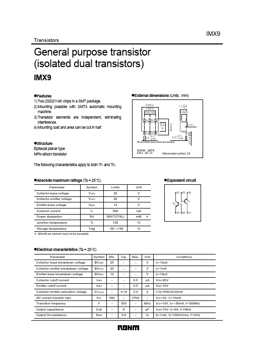
TransistorsGeneral purpose transistor (isolated dual transistors)IMX9z Features1) Two 2SD2114K chips in a SMT package.2) Mounting possible with SMT3 automatic mounting machine.3) Transistor elements are independent, eliminating interference.4) Mounting cost and area can be cut in half.z StructureEpitaxial planar type NPN silicon transistorThe following characteristics apply to both Tr 1 and Tr 2.z External dimensions (Units : mm)z Absolute maximum ratings (T a = 25°C)z Equivalent circuitParameterSymbol Limits Unit V CBO 25V V CEO 20V V EBO 12V I C 500mA Tj 150°C Tstg−55~+150°CPd 300(TOTAL)mW ∗Collector-base voltage Collector-emitter voltage Emitter-base voltage Collector current Junction temperature Storage temperaturePower dissipation ∗ 200mW per element must not be exceeded.z Electrical characteristics (T a = 25°C)ParameterSymbol BV CBO BV CEO BV EBO I CBO I EBO h FE V CE(sat)Min.252012−−560−−−−−−−0.18−−−0.50.527000.4V I C =10µA I C =1mA I E =10µA V CB =20V V EB =10VV CE =3V, I C =10mAI C /I B =500mA/20mA V V µA µA −V Typ.Max.Unit Conditionsf T RonCob −−−3500.88−−−V CE =10V, I E =−50mA, f =100MHz I B =1mA, V i =100mVrms, f =1kHzV CB =10V, I E =0A, f =1MHz MHz ΩpF Collector-base breakdown voltage Collector-emitter breakdown voltage Emitter-base breakdown voltage Collector cutoff current Emitter cutoff currentDC current transfer ratio Transition frequency Output capacitance Output On-resistanceCollector-emitter saturation voltageTransistorsz Packaging specificationsIMX9Part No.T1103000Packaging type CodeBasic ordering unit (pieces)Taping z Electrical characteristic curvesC O L L E C T O R C U R R E N T : I C(m A )COLLECTOR TO EMITTER VOLTAGE : V CE (V)Fig.1 Grounded emitter outputcharacteristics(Ι)C O L L E C T O R C U R R E N T : I C (m A )COLLECTOR TO EMITTER VOLTAGE : V CE (V)Fig.2 Grounded emitter outputcharacteristics (ΙΙ)C O L L E C T O R C U R R E N T : I C (m A )BASE TO EMITTER VOLTAGE : V BE (V)Fig.3 Grounded emitter propagationcharacteristicsD C C U R RE N T G A I N : hF ECOLLECTOR CURRENT : I C (mA)Fig.4 DC current gain vs. collectorcurrent (Ι)D C C U R RE N T G A IN : h F ECOLLECTOR CURRENT : I C (mA)Fig.5 DC current gain vs.collector current (ΙΙ)C O L L E C T O R S A T U R A T I O N V O L T A G E : V C E (s a t ) (m V )COLLECTOR CURRENT : I C (mA)Fig.6 Collector-emitter saturationvoltage vs. collector current (Ι)TransistorsC O L L E C T O R S A T U R A T I O N V O L T A G E : V C E (s a t ) (m V )COLLECTOR CURRENT : I C (mA)Fig.7 Collector-emitter saturationvoltage vs. collector current (ΙΙ)B A S E S A T U R A T I O N V O L T A G E : V B E (s a t ) (m V )COLLECTOR CURRENT : I C (mA)Fig.8 Base-emitter saturationvoltage vs. collector current (Ι)B A S E S A T U R A T I O N V O L T A G E : V B E (s a t ) (m V )COLLECTOR CURRENT : I C (mA)Fig.9 Base-emitter saturation voltagevs. collector current (ΙΙ)EMITTER CURRENT : I E (mA)T R A N S I T I O N F R E Q U E N C Y : f T (M H z )Fig.10 Gain bandwidth product vs.emitter currentC O L L E C T O R O U T P U T C A P A C I T A N C E : C o b (p F )COLLECTOR TO BASE VOLTAGE : V CB(V)Fig.11 Collector output capacitancevs. collector-base voltageO N R E S I S T A N C E: R o n (Ω)BASE CURRENT : I B (mA)Fig.12 Output-on resistance vs.base currentz Ron measurement circuitRon = ×R LV 0Vi-V 0V 0Input Vi 1kHzAppendixAbout Export Control Order in JapanProducts described herein are the objects of controlled goods in Annex 1 (Item 16) of Export Trade ControlOrder in Japan.In case of export from Japan, please confirm if it applies to "objective" criteria or an "informed" (by MITI clause)on the basis of "catch all controls for Non-Proliferation of Weapons of Mass Destruction.Appendix1-Rev1.0。
KAIJO910焊线机

第 1 章使用机台前为了长久使用本机台,在执行本机台的操作或与本机台相关的作业前,详细阅读所附的操作手册,理解使用中的注意事项,机台的概要,操作方法及与机台安全相关的事宜。
又,禁止擅自转载或复制本操作手册的全部或一部分供第三者使用。
目录1-1本文所记载的危险・警告・注意事项1-2保障与免除责任1-3使用中的注意事项(为了安全使用)1-1本文所记载的危险・警告・注意事项本机台的操作及保养手册把对人命,机台,产品的危险,作为危险程度分为【危险】,【警告】,【注意】3个阶段。
操作本机台之前,请仔细阅读所示注意事项,警告事项之后,正确使用。
●表示若无视此标识进行误操作或误作保养,可能导致重大事故或人员死亡危险的发生。
请遵守危险回避方法操作机器。
●表示若无视此标识,不严格遵守正确的操作手顺,正确的保养手顺,可能导致重伤事故的发生。
请根据灾害回避方法正确使用机器。
表示若无视此标识,不严格遵守正确的操作手顺,正确的保养手顺,可能导致伤害事故的发生。
请根据正确的操作及保养手顺正确使用机器。
另外,还有如下标识。
●表示记载了有关操作,保养中简便的产品功能,容易出错的事项,若不遵守或不纠正可能会导致产品本身损伤的各项事项。
1-2保证与免除责任机器保证规定如下。
保证期限1天使用8小时为基准,当地交货后1年内。
本机器的保证仅适用于故障原因明确为弊公司的场合。
责任不明确时,另行需要特别的同意。
无效保证期限内,下列情况不在保证范围内。
但,根据情况可提供修理。
(1)确定非弊公司的责任所造成的故障。
(2)由于天灾等不可抗拒的自然灾害引起的故障。
(3)未经弊公司的同意擅自改造本机台产生的故障(4)轴承,齿轮,回转轴,传送带,刀(叶片),螺母,电器控制零件,油消耗品的自然耗损。
(5)违反操作手册指示使用,操作,设置等引起的故障。
(6)机器的设定,保养,补给及调整作业点检不充分所引起的故障。
上述内容以外的项目,需另行签订个别协议。
1-3使用中的注意事项(为了安全使用机器)使用弊司的机器之前,为了安全请遵守下记注意事项。
KEMA 09ATEX0048 产品说明书

(13) SCHEDULE(14) to EC-Type Examination Certificate KEMA 09ATEX0048 Issue No. 4(15) DescriptionDifferential Pressure Transmitters DELTABAR M Model PMD55 and Pressure transmittersCERABAR M Model PMC51, Model PMP51 and Model PMP55 and DELTAPILOT M Model FMB50, Model FMB51, Model FMB52 and Model FMB53 are used in potentially explosive atmospheres caused by the presence of flammable gases, liquids, vapours or dusts for the measurement of level, flow, differential pressure, over- and under pressure.The pressure signal at the ceramic or metal sensor is converted into an electrical signal.The output of the Pressure or Differential Pressure Transmitter is a 4 - 20 mA current output signal with or without a superimposed HART digital signal, or the transmitter is intended to be connected to a fieldbus system (Profibus PA or Foundation Fieldbus).The several versions of the Pressure and Differential Pressure Transmitters differ in type of sensor, type of enclosure, process connection etc.Optionally all versions of the Pressure and Differential Pressure Transmitters may be provided with an indicator.Optionally, the display connector can be used for temporary connection of a service tool (e.g.Endress+Hauser Commubox type FXA191 or type FXA195).Optionally the Pressure Transmitters that are intended for application in explosive gas atmospheres, may be provided with a sensor with extension cable.Ambient temperature range -50 ºC to +70 ºC.The relation between temperature class, ambient temperature and process temperature is given in the following table.temperatureclassambienttemperatureprocess temperatureFMB50 FMB51 FMB52,FMB53PMD55 PMP55 1),PMC51, PMP51T6 ≤ 40 °C ≤ 80 °C ≤ 80 °C ≤ 80 °C ≤ 80 °C ≤ 80 °CT4 ≤ 70 °C ≤ 100 °C ≤ 85 °C ≤ 80 °C ≤ 120 °C ≤ 100 °C 2)T3 ≤ 70 °C ≤ 150 °CNOTE 1: Depending on the diaphragm seal used in model PMP55, a higher process temperature is permitted. For details, refer to the relevant equipment manual.NOTE 2: Process temperature for Models PMC51 and PMP51 with hygienic process connection ≤ 130 °C.. The maximum surface temperature of the enclosure T75 °C, respectively T500 100 °C (transmitters with interface 4 - 20 mA) or T500 105 °C (transmitters with Fieldbus interface) is b ased on the maximum ambient temperature of 70 °C for a dust lay er with a maximum thickness of 5 mm respectively 500 mm.(13) SCHEDULE(14) to EC-Type Examination Certificate KEMA 09ATEX0048 Issue No. 4Electrical dataTransmitters in type of protection intrinsic safety Ex iaInterface 4 - 20 mA (with or without HART communication):Supply and output circuit (terminals + and - or connector):in type of protection intrinsic safety Ex ia IIC, only for connection to a certified intrinsically safe circuit, with the following maximum values:U i = 30 V; I i = 300 mA; P i = 1 W; L i = 0 mH; C i = 10 nF.Interface Profibus PA or Foundation Fieldbus:Supply and data circuit (terminals + and - or connector):in type of protection intrinsic safety Ex ia IIC, only for connection to a certified intrinsically safecircuit, with the following maximum values:U i = 24 V; I i = 250 mA; P i = 1,2 W; L i = 10 µH; C i = 5 nF;or to an intrinsically safe fieldbus in accordance with FISCO, with the following maximum values: U i = 17,5 V; I i = 500 mA; P i = 5,5 W; L i = 10 µH; C i = 5 nF.Display connector:in type of protection intrinsic safety Ex ia IIC, for connection to a certified intrinsically safe circuit, with following maximum values:U o = 8,6 V; I o = 39 mA; P o = 124 mW andU i = 8,5 V; I i = 7 mA; P i = 10 mW; C i = 0 nF; L o = 0 mH.Transmitters in type of protection Ex tU max = 45 V (interface 4 - 20 mA), respectively 32 V (fieldbus interface).Installation instructionsThe instructions provided with the equipment shall be followed in detail to assure safe operation. (16) Test ReportNo. NL/KEM/ExTR09.0017/**.(17) Special conditions for safe useNone.(18) Essential Health and Safety RequirementsCovered by the standards listed at (9).(19) Test documentationAs listed in Test Report No. NL/KEM/ExTR09.0017/**.。
EZFK942FM中文资料

■ Characteristics
System EGSM DCS PCS Part No. EZFK897FM EZFK942FM EZFKH47FM EZFKJ42FM EZFKJ80FM EZFKK60FM Center Frequency (MHz) 897.5 942.5 1747.5 1842.5 1880.0 1960.0 Passband Width (MHz) ±17.5 ±17.5 ±37.5 ±37.5 ±30.0 ±30.0 Insertion Loss (dB) 4.6 5.8 3.5 3.5 3.2 3.0 Attenuation (dB)(MHz) 9.5 (925 to 960) 40 (880 to 915) 20 (1805 to 1880) 20 (1710 to 1785) 20 (1930 to 1990) 20 (1850 to 1910)
Design and specifications are each subject to change without notice. Ask factory for the current technical specifications before purchase and/or use. Should a safety concern arise regarding this product, please be sure to contact us immediately.
10.0
Mar. 2005
14.0
EZFK
Lot No.
FM
I/O
I/O 2.0 5.0
1.0
1.0 3.0 3.0 8.0 6.0
Design and specifications are each subject to change without notice. Ask factory for the current technical specifications before purchase and/or use. Should a safety concern arise regarding this product, please be sure to contact us immediately.
SEMIKRON ESD9L系列电路保护扇形电阻说明书

ESD9L, SESD9L Series Transient Voltage SuppressorsESD Protection Diodes with Ultra−Low CapacitanceThe ESD9L Series is designed to protect voltage sensitive components that require ultra−low capacitance from ESD and transient voltage events. Excellent clamping capability, low capacitance, low leakage, and fast response time, make these parts ideal for ESD protection on designs where board space is at a premium. Because of its low capacitance, it is suited for use in high frequency designs such as USB 2.0 high speed and antenna line applications.Specification Features:•Ultra Low Capacitance 0.5 pF •Low Clamping V oltage•Small Body Outline Dimensions:0.039″ x 0.024″(1.00 mm x 0.60 mm)•Low Body Height: 0.016″ (0.4 mm)•Stand−off V oltage: 3.3 V , 5 V •Low Leakage•Response Time is Typically < 1.0 ns •IEC61000−4−2 Level 4 ESD Protection•S and SZ Prefixes for Automotive and Other Applications Requiring Unique Site and Control Change Requirements; AEC−Q101Qualified and PPAP Capable•These Devices are Pb−Free and are RoHS CompliantMechanical Characteristics:CASE: V oid-free, transfer-molded, thermosetting plasticEpoxy Meets UL 94 V−0LEAD FINISH: 100% Matte Sn (Tin)MOUNTING POSITION: AnyQUALIFIED MAX REFLOW TEMPERATURE: 260°CDevice Meets MSL 1 RequirementsMAXIMUM RATINGSRatingSymbolValue Unit IEC 61000−4−2 (ESD)ContactAir±10±15kVTotal Power Dissipation on FR−5 Board (Note 1) @ T A = 25°C P D 150mW Storage Temperature Range T stg −55 to +150°CJunction Temperature Range T J −55 to +150°C Lead Solder Temperature − Maximum(10 Second Duration)TL 260°CStresses exceeding those listed in the Maximum Ratings table may damage the device. If any of these limits are exceeded, device functionality should not be assumed, damage may occur and reliability may be affected.1.FR−5 = 1.0 x 0.75 x 0.62 in.See Application Note AND8308/D for further description of survivability specs.Device PackageShipping †ORDERING INFORMATIONSOD−923CASE 514ABESD9LxxxST5G SOD−923(Pb−Free)8000/T ape & Reel MARKING DIAGRAMSee specific marking information in the device marking column of the Electrical Characteristics tables starting on page 2 of this data sheet.DEVICE MARKING INFORMATION†For information on tape and reel specifications,including part orientation and tape sizes, please refer to our T ape and Reel Packaging Specifications Brochure, BRD8011/D.X = Specific Device Code M = Date Code*Date Code orientation and/or position may vary depending upon manufacturing location.PIN 1.CATHODE2.ANODE12122SESD9LxxxST5G SOD−923(Pb−Free)8000/T ape & Reel SZESD9LxxxST5GSOD−923(Pb−Free)8000/T ape & ReelELECTRICAL CHARACTERISTICS(T A = 25°C unless otherwise noted)Symbol ParameterI PP Maximum Reverse Peak Pulse Current V C Clamping Voltage @ I PP V RWM Working Peak Reverse VoltageI R Maximum Reverse Leakage Current @ VRWM V BR Breakdown Voltage @ I T I T Test Current I F Forward Current V F Forward Voltage @ I F P pk Peak Power DissipationCMax. Capacitance @ V R = 0 and f = 1.0 MHz*See Application Note AND8308/D for detailed explanations of datasheet parameters.ELECTRICAL CHARACTERISTICS (T A = 25°C unless otherwise noted, V F = 1.0 V Max. @ I F = 10 mA for all types)Device*Device Marking V RWM (V)I R (m A)@ VRWM V BR (V) @ I T (Note 2)I T C (pF)V C (V)@ I PP = 1 AV CMax Max Min mA Typ Max Max Per IEC61000−4−2(Note 4)ESD9L3.3ST5G 6** 3.3 1.0 4.8 1.00.50.99.0Figures 1 and 2See Below ESD9L5.0ST5GD5.01.05.41.00.50.99.8Figures 1 and 2See Below*Includes S and SZ-prefix devices where applicable.**Rotated 180°.2.V BR is measured with a pulse test current I T at an ambient temperature of 25°C.3.Surge current waveform per Figure 5.4.For test procedure see Figures 3 and 4 and Application Note AND8307/D.Figure 1. ESD Clamping Voltage Screenshot Positive 8 kV Contact per IEC61000−4−2Figure 2. ESD Clamping Voltage Screenshot Negative 8 kV Contact per IEC61000−4−2IEC 61000−4−2 Spec.Level Test Volt-age (kV)First Peak Current (A)Current at 30 ns (A)Current at 60 ns (A)127.5422415843622.51264830168IEC61000−4−2 WaveformFigure 3. IEC61000−4−2 SpecOscilloscopeThe following is taken from Application NoteAND8308/D − Interpretation of Datasheet Parameters for ESD Devices.ESD Voltage ClampingFor sensitive circuit elements it is important to limit the voltage that an IC will be exposed to during an ESD event to as low a voltage as possible. The ESD clamping voltage is the voltage drop across the ESD protection diode during an ESD event per the IEC61000−4−2 waveform. Since the IEC61000−4−2 was written as a pass/fail spec for largersystems such as cell phones or laptop computers it is not clearly defined in the spec how to specify a clamping voltage at the device level. ON Semiconductor has developed a way to examine the entire voltage waveform across the ESD protection diode over the time domain of an ESD pulse in the form of an oscilloscope screenshot, which can be found on the datasheets for all ESD protection diodes. For more information on how ON Semiconductor creates these screenshots and how to interpret them please refer to AND8307/D.Figure 5. 8 X 20 ms Pulse Waveform1009080706050403020100t, TIME (m s)% O F P E A K P U L S E C U R R E N TPACKAGE DIMENSIONSSOD−923CASE 514AB ISSUE CNOTES:1.DIMENSIONING AND TOLERANCING PER ASME Y14.5M, 1994.2.CONTROLLING DIMENSION: MILLIMETERS.3.MAXIMUM LEAD THICKNESS INCLUDES LEAD FINISH. MINIMUM LEAD THICKNESS IS THE MINIMUM THICKNESS OF BASE MATERIAL.4.DIMENSIONS D AND E DO NOT INCLUDE MOLD FLASH, PROTRUSIONS, OR GATE BURRS.DIM MIN NOM MAX MILLIMETERS A 0.340.370.40b 0.150.200.25c 0.070.120.17D 0.750.800.85E 0.550.600.650.95 1.00 1.05L 0.19 REF H E 0.0130.0150.0160.0060.0080.0100.0030.0050.0070.0300.0310.0330.0220.0240.0260.0370.0390.0410.007 REFMIN NOM MAX INCHEScADIMENSIONS: MILLIMETERS*For additional information on our Pb−Free strategy and soldering details, please download the ON Semiconductor Soldering and Mounting Techniques Reference Manual, SOLDERRM/D.SOLDERING FOOTPRINT*See Application Note AND8455/D for more mounting details 2X0.252XOUTLINE2X0.08X YTOP VIEW2XBOTTOM VIEWL2XL20.050.100.150.0020.0040.006ON Semiconductor and are trademarks of Semiconductor Components Industries, LLC dba ON Semiconductor or its subsidiaries in the United States and/or other countries.ON Semiconductor owns the rights to a number of patents, trademarks, copyrights, trade secrets, and other intellectual property. A listing of ON Semiconductor’s product/patent PUBLICATION ORDERING INFORMATION。
K-9可选配件,微维克斯硬度试验机剪子订单号型号及描述说明书
G
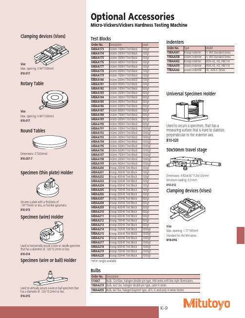
steel ball 1471N(150kgf) beryllium copper, phosphor bronze
H
1/8”
588.4N(60kgf) Bearing metal
E
diameter 980.7N(100kgf)
K
steel ball 1471N(150kgf)
L
1/4”
588.4N(60kgf) Plastics, lead
50x50mm travel stage
Dimensions: 4.92x4.92”(125x125mm) Minimum reading: 0.01mm 810-012
Clamping devices (Vises)
Vise Max. opening: 1.77”(45mm) Standard for the MH series. 810-016
Indenters
Order No. 19BAA061 19BAA058 19BAA062 19BAA059 19BAA060
Type Knoop Indenter Vickers Indenter Knoop Indenter Vickers Indenter Vickers Indenter
Model H, HM Standard Series H, HM Standard Series MVK-H2, H3, HM114 MVK-H2, H3, HM114 HV, AVK-C Series
Micro-Vickers/Vickers Hardness Testing Machine
Test Blocks
Order No. 64BAA173 64BAA174 64BAA175 64BAA176 64BAA177 64BAA178 64BAA179 64BAA180 64BAA181 64BAA182 64BAA183 64BAA184 64BAA185 64BAA186 64BAA187 64BAA188 64BAA189 64BAA190 64BAA191 64BAA192 64BAA193 64BAA194 64BAA195 64BAA196 64BAA197 64BAA198 64BAA199 64BAA200 64BAA201 64BAA202 64BAA203 64BAA204 64BAA205 64BAA206 64BAA207 64BAA208 64BAA209 64BAA210 64BAA211 64BAA212 64BAA213 64BAA214 64BAA215 64BAA216 64BAA217 64BAA218 64BAA219 64BAA220
Freescale Kinetis E 系列 KE06 微控制器开发板用户指南说明书
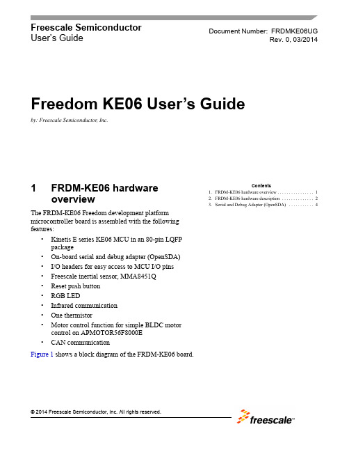
Freescale Semiconductor User’s Guide1FRDM-KE06 hardware overviewThe FRDM-KE06 Freedom development platform microcontroller board is assembled with the following features:•Kinetis E series KE06 MCU in an 80-pin LQFP package•On-board serial and debug adapter (OpenSDA)•I/O headers for easy access to MCU I/O pins •Freescale inertial sensor, MMA8451Q •Reset push button •RGB LED•Infrared communication •One thermistor•Motor control function for simple BLDC motor control on APMOTOR56F8000E •CAN communication Figure 1 shows a block diagram of the FRDM-KE06 board.Document Number:FRDMKE06UGRev. 0, 03/2014Contents1.FRDM-KE06 hardware overview . . . . . . . . . . . . . . . . 12.FRDM-KE06 hardware description . . . . . . . . . . . . . . 23.Serial and Debug Adapter (OpenSDA) . . . . . . . . . . . 4Freedom KE06 User’s Guideby: Freescale Semiconductor, Inc.FRDM-KE06 hardware descriptionFigure1. FRDM-KE06 block diagramThe FRDM-KE06 features two microcontrollers, the target MCU and a serial and debug adapter (OpenSDA) MCU. The target MCU is a Kinetis E series KE06 family device. The OpenSDA MCU is a Kinetis K series K20 family device, the K20DX128VFM5.2FRDM-KE06 hardware description2.1Power supplyThe FRDM-KE06 offers a design with multiple power supply options. It can be powered from the USB connector, the V IN pin on the I/O header, an off-board 1.71-3.6V supply from the 3.3V pin on the I/O header or 3.3V from motor control board. The USB and V IN supplies are regulated on-board using a 3.3V linear regulator to produce the main power supply. The other two sources are not regulated on-board. Note that KE06 on FRDM board can be powered by 5V or 3.3V.The following figure shows the schematic drawing for the power supply inputs and the on-board voltage regulator.FRDM-KE06 hardware descriptionFigure 2. FRDM-KE06 power supplyTable 1 provides the operational details and requirements for the power supplies.Note that the OpenSDA circuit is only operational when a USB cable is connected and supplying power to J6. However, the protection circuitry is in place to allow multiple sources to be powered at once.Table 1. Power supply requirementsSupply Source Valid RangeOpenSDA Operational?Regulated on-board?OpenSDA USB (J6)5VYes Yes V IN Pin on I/O header 4.3-9V Yes Yes 3.3V Pin on I/O header 1.71-3.6V Yes No 3.3V Pin on motor control header3.3VYesNoTable 2. Power suppliesPower Supply Name DescriptionVDD_PERIPHPeripheral power supply, including RGB LED, Key buttons, infrared, thermistor, reset circuit.J14 Pin1&2 connected, 3.3V power supply;J14 Pin2&3 connected, 5V power supply.Serial and Debug Adapter (OpenSDA)Notes:1.J9 and J10 are not populated by default on the production version. The two pins of these headers are shorted together by 0 ohm resistor R12 and R26 on the PCB. To measure the energyconsumption of either the KE06 or the OpenSDA MCU, the 0 ohm resistor between these pins must first be cut. A current probe or a shunt resistor and voltage meter can then be applied to measure the energy consumption on these rails. When the MCU current measurement is done, this 0 ohm resistor can be soldered on again.2.To better get ADC accuracy on KE06, it is recommended that a 0 ohm resistor R13 be soldered on. Ensure there is no power supply from P3V3_MOTOR and P3V3 sourced from I/O headers.3Serial and Debug Adapter (OpenSDA)OpenSDA is an open-standard serial and debug adapter. It bridges serial and debug communications between a USB host and an embedded target processor as shown in Figure 3.VDD_KE06KE06 MCU power supply.Header J9 provides a convenient means for KE06 energy consumption measurements.Header J14 for KE06 power supply selection: 3.3V or 5V.J14 Pin1&2 connected, 3.3V power supply,J14 Pin2&3 connected, 5V power supply.P3V3_SDAOpenSDA circuit power supply. Can be 3.3V only.Header J10 provides a convenient means for K20 energy consumption measurements.P5V_SDA INPUT [J6 Pin1] Input 5V Power supplied from the OpenSDA USB connector. P5-9V_VIN INPUT [J4 Pin16] Power supplied from the V IN pin of the I/O headers.P3V3_MOTOR INPUT [J2 Pin13] Input 3.3V power supplied from motor control header.P5V_USB OUTPUT[J4 Pin10] Output 5V to the I/O headers.Sourced from J6 USB (P5V_SDA) supply through a back drive protection Schottky diode.Table 2. Power suppliesSerial and Debug Adapter (OpenSDA)Figure3. OpenSDA block diagramOpenSDA is managed by a Kinetis K20 MCU built on the ARM® Cortex™-M4 core. The OpenSDA circuit includes a status LED (D4) and a reset pushbutton (SW1). The pushbutton asserts the reset signal to the KE06 target MCU. It can also be used to place the OpenSDA circuit into Bootloader mode by holding down the reset pushbutton while plugging the USB cable to USB connector J6. Once the OpenSDA enters bootloader mode, other OpenSDA applications such as debug app can be programmed. SPI and GPIO signals provide an interface to the SWD debug port of the KE06. Additionally, signal connections are available to implement a UART serial channel. The OpenSDA circuit receives power when the USB connector J6 is plugged into a USB host.3.1Debugging InterfaceSignals with SPI and GPIO capability are used to connect directly to the SWD of the KE06. These signals are also brought out to a standard 10-pin (0.05”) Cortex Debug connector (J7) as shown in Figure 4. It is possible to isolate the KE06 MCU from the OpenSDA circuit and use J7 to connect to an off-board MCU. To accomplish this, cut the 0 ohm resistor R58. This will disconnect the SWD_CLK pin to the KE06 so that it will not interfere with the communications to an off-board MCU connected to J7.When KE06 on FRDM board is 5V powered, and the OpenSDA is power off, there need to connect an external debugger to debug KE06 on board.Serial and Debug Adapter (OpenSDA)Figure4. SWD debug connector to KE063.2Virtual Serial PortA serial port connection is available between the OpenSDA MCU and UART1 pin PTC7 (TXD1) and PTC6 (RXD1) of KE06. Several of the default OpenSDA applications provided by Freescale, including the MSD Flash Programmer and the P&E Debug Application, provide a USB Communications Device Class (CDC) interface that bridges serial communications between the USB host and this serial interface on the KE06.3.3KE06 Microcontroller3.3.1Clock SourceThe Kinetis KE06 microcontrollers feature an on-chip oscillator compatible with two ranges of input crystal or resonator frequencies: 32 kHz (low frequency mode), 4-20 MHz (high frequency mode).The KE06 on the FRDM-KE06 is clocked from an 8 MHz crystal.3.3.2Serial PortThe serial port interface signals used with OpenSDA are UART1 pin PTC7 (TXD1) and PTC6 (RXD1). These signals are also connected to I/O header J1.3.3.3ResetThe PTA5/RESET signal on the KE06 is connected externally to a pushbutton SW1. The reset button can be used to force an external reset event in the target MCU. The reset button can also be used to force the OpenSDA circuit into bootloader mode when plugging the USB cable to J6. See Section3, “Serial and Debug Adapter (OpenSDA)” section for more details.Serial and Debug Adapter (OpenSDA)3.3.4DebugThe sole debug interface on all Kinetis E Series devices is a Serial Wire Debug (SWD) port. The primary controller of this interface on the FRDM-KE06 is the onboard OpenSDA circuit. However, a 2x5-pin (0.05”) Cortex Debug connector, J7, provides access to the SWD signals for the KE06 MCU. The following table shows SWD connector signals description for KE06:3.4ThermistorOne thermistor (RT1) is connected to two ADC inputs (PTF4/ADP12, PTF5/ADP13) of KE06 for evaluating the ADC module.Figure 5. Thermistor connectionTable 3. ARM JTAG/SWD mini Connector DescriptionPin FunctionConnection to KE061VTref 3.3V or 5V KE06 power supply (VDD_KE06)2SWDIO/TMS PTA4/SWD_DIO 3GNDGND4SWDCLK/TCK PTC4/SWD_CLK 5GND GND 6SWO/TDO NC 7NC NC 8TDI NC 9NC NC10RESETPTA5/RESETSerial and Debug Adapter (OpenSDA)3.5Infrared PortOne infrared Rx port and one Tx port (as shown in the following figure) are connected to ACMP0 input pin (ACMP0_IN1) and UART0 TXD0 pin of KE06 to demonstrate the capability of SCI0 modulated by a flextimer to generate infrared signals and use ACMP0 as a filter to receive the SCI data via infrared signal.Figure6. Infrared connection3.6Key buttonsTwo key buttons are connected to PTH3/4 to demonstrate KBI function of KE06, which can capture both falling edge and rising edge of key button input, as shown in the following figure.Serial and Debug Adapter (OpenSDA)Figure7. Key buttons connection3.7Three-axis accelerometerA Freescale MMA8451Q low power, three-axis accelerometer is interfaced through an I2C bus and two GPIO signals as shown in the following table. By default, the I2C address is 0x1D (SA0 pulled high).Table4. Accelerometer signal connectionsMMA8451Q KE06SCL PTA3SDA PTA2INT1 PTD4INT2 PTD3Serial and Debug Adapter (OpenSDA)Figure8. Accelerometer connection3.8RGB LEDThree PWM-capable pins are connected to a red, green, blue LED. The signal connections are shown in the table below.Table5. RGB LED Signal ConnectionsRGB LED KE06Red Cathode PTG5/FTM2CH3Green Cathode PTG6/FTM2CH4Blue Cathode PTG7/FTM2CH5Serial and Debug Adapter (OpenSDA)Figure9. GB LED connection3.9CANThe CAN phy on KE06 FRDM board is 3.3V powered.Table6. CAN signal connectionCAN Phy KE06D CAN_TXR CAN_RXSerial and Debug Adapter (OpenSDA)Figure10. CAN3.10Input/Output HeadersThe KE06 microcontroller is packaged in an 80-pin LQFP. Some pins are utilized in on-board circuitry, but many are directly connected to one of four I/O headers (J1, J2, J3, J4 and J5). J1 and J2 also function as motor control headers to provide access to a motor control board such as simple BLDC motor driving board APMOTOR56F8000E.Serial and Debug Adapter (OpenSDA)Figure11. I/O headers3.11Arduino CompatibilityThe I/O headers on the FRDM-KE06 are arranged to allow compatibility with peripheral boards (known as shields) that connect to Arduino and Arduino-compatible microcontroller boards. The pins on the headers share the same mechanical spacing and placement as the I/O headers on the Arduino Uno Revision 3 board design. See Figure11 for compatible signals.Document Number:FRDMKE06UG Rev. 003/2014Information in this document is provided solely to enable system and software implementers to use Freescale products. There are no express or implied copyright licenses granted hereunder to design or fabricate any integrated circuits based on the information in this document.Freescale reserves the right to make changes without further notice to any products herein. Freescale makes no warranty, representation, or guarantee regarding the suitability of its products for any particular purpose, nor does Freescale assume any liability arising out of the application or use of any product or circuit, and specifically disclaims any and all liability, including without limitation consequential or incidental damages. “Typical” parameters that may be provided in Freescale data sheets and/or specifications can and do vary in different applications, and actual performance may vary over time. All operating parameters, including “typicals,” must be validated for each customer application by customer’s technical experts. Freescale does not convey any license under its patent rights nor the rights of others. Freescale sells products pursuant to standard terms and conditions of sale, which can be found at the following address: /SalesTermsandConditions.How to Reach Us:Home Page:Web Support:/supportFreescale, the Freescale logo, and Kinetis, are trademarks of FreescaleSemiconductor, Inc., Reg. U.S. Pat. & Tm. Off. All other product or service names arethe property of their respective owners. ARM and Cortex are the registered trademarksof ARM Limited. ARMCortex-M4 is the trademark of ARM Limited.© 2014 Freescale Semiconductor, Inc.。
装配式热电偶
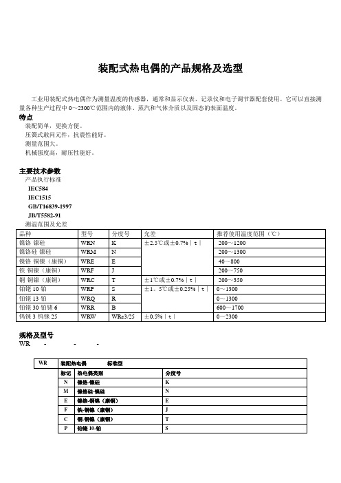
装配式热电偶的产品规格及选型工业用装配式热电偶作为测量温度的传感器,通常和显示仪表、记录仪和电子调节器配套使用。
它可以直接测量各种生产过程中0~2300℃范围内的液体、蒸汽和气体介质以及固态的表面温度。
特点装配简单,更换方便。
压簧式敢问元件,抗震性能好。
测量范围大。
机械强度高,耐压性能好。
主要技术参数产品执行标准IEC584IEC1515GB/T16839-1997JB/T5582-91测温范围及允差品种型号分度号允差推荐使用温度范围(℃)镍铬-镍硅WRN K ±2.5℃或±0.7%∣t∣-200~1200镍铬硅-镍硅WRM N -200~1300镍铬-铜镍(康铜)WRE E -40~800铁-铜镍(康铜)WRF J -200~750铜-铜镍(康铜)WRC T ±1℃或±0.7%∣t∣-200~350铂铑10-铂WRP S ±1。
5℃或±0.25%∣t∣0~1300铂铑13-铂WRQ R 0~1300铂铑30-铂铑6 WRR B 600~1700钨铼3-钨铼25 WRW WRe3/25 ±0.5%∣t∣0~2300规格及型号WR - - -WR 装配热电偶标准型标记热电偶类别分度号N 镍铬-镍硅KM 镍铬硅-镍硅NE 镍铬-铜镍(康铜) EF 铁-铜镍(康铜)JC 铜-铜镍(康铜)TP 铂铑10-铂SQ 铂铑13-铂RR 铂铑30-铂铑6 BW 钨铼3-钨铼25 WRe3/25标记热电偶对数1 单支式2 双支式标记安装固定方式1 无固定装置2 固定螺纹3 活动法兰4 固定法兰5 活络管接头式6 锥形固定螺纹7 直形管接头式8 固定螺纹管接头式9 活动螺纹接头式标记接线盒形式2 防溅式3 防水式4 防爆式标记保护管直径(mm)0 ¢161 ¢20(S、R、B型热电偶为¢25双层管)2 ¢16(高铝管、限用于K、N型热电偶)3 ¢25(高铝管、限用于K、N型热电偶)标记测量端形式X 接壳型(小惰性热电偶限用于K、N、E型)无标记绝缘型总长L (mm)标记保护管材质B 1Cr18Ni9TiA 碳钢20C Cr25TiR 刚玉质Q 高铝质MS 二硅化钼SC 碳化硅X 特殊保护管订货时加以说明插入长度l(mm)标记隔爆等级BT4 dIIBT4CT4 dIICT4。
集成晶体振荡器产品手册

1.25~100 ±0.5~5 -55~+85℃ 1.25~300 ±0.5~5 -55~+85℃
12/5 12/5
S/T/H/C S/T/H/C
MP2525 MP3030 MP3232 MP3627 MP4025
TXM11 系列 (表面贴装) 10~30 ±1~5 -30~+85℃ 5/3.3 T/H/C
fT=±(fmax-fmin)/(fmax+fmin) fTref=±MAX〔|(fmax-fref)/ fref|,|(fmin-fref)/ fref| fT:频率温度稳定度(不带隐含基准温度) fTref:频率温度稳定度(带隐含基准温度) fmax:规定温度范围内测得的最高频率 fmin:规定温度范围内测得的最低频率 fref:规定基准温度测得的频率
0.5
5
OX50 系列
10~100
±0.005~0.2
/
0.5
5
OXLN 系列 (超低相噪)
10、~0.3
-155/-170(SC) -147/-170(AT)
0.5
7
*:S-Sinewave;T-TTL;H-HCMOS;C-Clipped Sine
MP2525 MP3030 MP3627 MP3838 MP5050
TX12 系列
10~35 ±0.5~5 -40~+85℃ 5/3.3 T/H/C
DIP14
TX14 系列
10~100 ±0.5~5 -40~+85℃ 12/5 S/T/H/C
DIP14D
TX20 系列
1.25~100 ±0.5~5 -55~+85℃ 12/5 S/T/H/C
K9F2G08U0M-PCB0中文资料
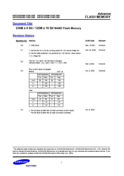
2
元器件交易网
K9F2G08Q0M-YCB0,YIB0 K9F2G08U0M-YCB0,YIB0
K9F2G16Q0M-YCB0,YIB0 K9F2G16U0M-YCB0,YIB0
Advance FLASH MEMORY
PIN CONFIGURATION (TSOP1)
K9F2GXXX0M-YCB0/YIB0 X16
Draft Date
Sep. 19.2001 Nov. 22. 2002
Remark
Advance Advance
0.2
Mar. 6.2003
Advance
0.3
Few current value is changed. Before K9F2G08Q0M Typ. ISB2 ILI ILO After K9F2G08Q0M Typ. ISB2 ILI ILO 10 Max. 50 ±10 ±10 20 Max. 100 ±20 ±20
N.C N.C N.C N.C N.C N.C R/B RE CE N.C N.C Vcc Vss N.C N.C CLE ALE WE WP N.C N.C N.C N.C N.C
X8
N.C N.C N.C N.C N.C N.C R/B RE CE N.C N.C Vcc Vss N.C N.C CLE ALE WE WP N.C N.C N.C N.C N.C 1 2 3 4 5 6 7 8 9 10 11 12 13 14 15 16 17 18 19 20 21 22 23 24 48 47 46 45 44 43 42 41 40 39 38 37 36 35 34 33 32 31 30 29 28 27 26 25
X8
N.C N.C N.C N.C I/O7 I/O6 I/O5 I/O4 N.C N.C PRE Vcc Vss N.C N.C N.C I/O3 I/O2 I/O1 I/O0 N.C N.C N.C N.C
丹福斯690V电机驱动器系列产品介绍说明书

Dedicated enclosure sizes down to 1.1 kW No need for large over-dimensioned drive Operate motors down to 0.37 kW No need for step-down transformerSmallest size and required spaceCost for cabinet and installation room reduced Side-by-side mounting without derating Saves valuable panel spaceIntegrated harmonic filters (<40% THiD)Maintain mains quality without external filters Integrated EMC filter (A1/EN 55011) with up to 150 m screened motor cableProvide reliable operation of the installation without additional external filtersClass 3C3 conformal coating (IEC60721-3-3) as standardIncrease lifetime and reliability in harsh environmentsFull performance at 50˚C ambient temperature (D-frames 45˚C)Secure operation without derating/over-dimensioningDanfoss output filtersMatching Sine-Wave or du/dt filtersComplete range of 690V drives up to 1.4 MWOne drive series covers all your system needsDanfoss makes 690 V installations most cost efficient. The high perfor-mance frequency converters now cover the complete 690 Vpower range from 1.4 MW down to 1.1 kW.Danfoss presents the smallest 690 V enclosure on the market below 7.5 kW and extends the power range of its IP 20 drives up to 75 kW with 4 new enclosure sizes.Now you can even control 690 V mo-tors down to 0.37 kW without expen-sive over-dimensioned drives or step down transformers.Built on the powerful and reliable VLT® platform, the drives off er system designers, machine builders, and end users the efficiency enhancing benefits offered by Danfoss’ single drive concept for industrial applications.Suitable for use on normal TN and IT (isolated) grids, the IP 20 protectedd rives are especially useful in installa-tions within chemical, mining, water/wastewater and marine applications./drives65%less cabinet space requiredEspecially for power sizes below 7.5 kW, Danfoss offers a remarkable spacereduction in comparison to other solutions.Technical dataVLT® power rating: Power ratings correspond to both HO and NO ratingsBrake resistors2VLT® drives for 690 V | 1.1 kW – 75 kW |IMPORTANT INSTALLATION INSTRUCTIONSDanfoss recommends that all drives below 7.5 kW should be installedwith output filters, unless the manufacturer specifically confirms that the motors comply with IEC60034-25 curve B for 690 V. If the motor is converter rated, but not for 690 V – then a du/dt filter is needed. In all other situations a sine-wave filter should be used.ATEX-certified thermistor inputThe PTB ATEX-certified VLT® PTC Thermistor Card MCB 112 can be used to monitor both Ex d and Ex e motors.It is certified according to IEC 61508 for use in low demand ap-plications to protect motors placed in zones 1, 2, 21 and 22. The option can be used as the sole protective device of an explosion-proof motor operated by a frequency converter.Universal residual current monitoringThe RCMB20/35 external fault current monitoring module reliably detects insulation faults in drives systems operating on IT or TN mains.In addition to usual pro-tection against suddeninsulation faults, this modulesupports preventive maintenance by detecting gradual insulation deterioration in the equipment in advance, avoiding unexpected andexpensive machine standstills.Sine-Wave Filtersdu/dt FiltersVLT® AutomationDrivef requency converters can be individually configured with additional safety functions through special options andaccessories.| 1.1 kW – 75 kW | VLT® drives for 690 V3Danfoss extends the power range of its IP 20 drives up to 75 kWwith 4 new enclosure sizes.B4A3C3D3h1) FC 102 only 2)FC 202 only 3)FC 302 only* F or upgrade from Enclosure type IP 20 to IP 21, an additional IP 21/NEMA 1 kit is required** 1.1 – 7.5 kW power sizes always include brake chopper[1][2][3][4][5][6][7][8][9][10][11][12][13][14][15][16][17][18][19][20]DKDD.PM.402.A3.02 VLT® is a trademark of Danfoss A/S Produced by PE-MSMBM 2014.09Ordering typecode for 690 V IP 20 drives (1.1 – 75 kW)See High Power Drives Selection Guide for ordering typecodes for power sizes > 90 kWDanfoss VLT Drives , Ulsnaes 1, DK-6300 Graasten, Denmark, Tel. +45 74 88 22 22, Fax +45 74 65 25 /drives,E-mail:****************。
贴片电容选型
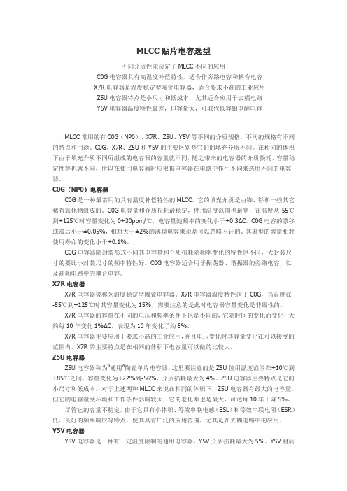
MLCC贴片电容选型不同介质性能决定了MLCC不同的应用C0G电容器具有高温度补偿特性,适合作旁路电容和耦合电容X7R电容器是温度稳定型陶瓷电容器,适合要求不高的工业应用Z5U电容器特点是小尺寸和低成本,尤其适合应用于去耦电路Y5V电容器温度特性最差,但容量大,可取代低容铝电解电容MLCC常用的有C0G(NP0)、X7R、Z5U、Y5V等不同的介质规格,不同的规格有不同的特点和用途。
C0G、X7R、Z5U和Y5V的主要区别是它们的填充介质不同。
在相同的体积下由于填充介质不同所组成的电容器的容量就不同,随之带来的电容器的介质损耗、容量稳定性等也就不同,所以在使用电容器时应根据电容器在电路中作用不同来选用不同的电容器。
C0G(NP0)电容器C0G是一种最常用的具有温度补偿特性的MLCC。
它的填充介质是由铷、钐和一些其它稀有氧化物组成的。
C0G电容量和介质损耗最稳定,使用温度范围也最宽,在温度从-55℃到+125℃时容量变化为0±30ppm/℃,电容量随频率的变化小于±0.3ΔC。
C0G电容的漂移或滞后小于±0.05%,相对大于±2%的薄膜电容来说是可以忽略不计的。
其典型的容量相对使用寿命的变化小于±0.1%。
C0G电容器随封装形式不同其电容量和介质损耗随频率变化的特性也不同,大封装尺寸的要比小封装尺寸的频率特性好。
C0G电容器适合用于振荡器、谐振器的旁路电容,以及高频电路中的耦合电容。
X7R电容器X7R电容器被称为温度稳定型陶瓷电容器。
X7R电容器温度特性次于C0G,当温度在-55℃到+125℃时其容量变化为15%,需要注意的是此时电容器容量变化是非线性的。
X7R电容器的容量在不同的电压和频率条件下也是不同的,它随时间的变化而变化,大约每10年变化1%ΔC,表现为10年变化了约5%。
X7R电容器主要应用于要求不高的工业应用,并且电压变化时其容量变化在可以接受的范围内,X7R的主要特点是在相同的体积下电容量可以做的比较大。
EB-9V Battery-powered Automatic Flashing Module Us

KUTAI ELECTRONICS INDUSTRY CO., LTD.TEL : +886-7-8121771FAX : +886-7-8121775Website : Headquarters : No.3, Ln. 201, Qianfu St., Qianzhen Dist., Kaohsiung City 806037, TaiwanEB-9VBattery-powered Automatic Flashing ModuleUser Manual※Lithium Battery Not IncludedSECTION 1 : FEATURES●No external battery or DC power supply required, excitation power provided by an internal battery.●Small size, light weight and easy installation saving labor.●Automatic excitation detection requires no manual operation or settings.●Very low static power consumption, Up to 3 years between battery replacement in standby mode.●Excitation function repeats 3 times and stops automatically when voltage is established.●Battery low voltage indicator reminds user to change battery.●Up to three repeat flashing attempts and will automatically stop when voltage builds up.●Excitation failure indicator. Resets automatically when voltage builds up or engine is stopped.●Battery reverse polarity protection.●Excitation field F+, F- Reverse Polarity Protection.●Built in manual forced excitation push button.SECTION 2 : SPECIFICATIONSensing Voltage Input Lithium Battery SpecificationsVoltage 1 300 Vac 1 phase 2 wire Model no. Ultralife U9VL-J-PFrequency 50/60 Hz Voltage 9 VdcCurrent Normal discharge 700 mA Max Excitation Output Pulse discharge 1050 mA MaxVoltage 9 Vdc Capacity 1200 mAh @ 23 ˚CCurrent 700 mA Max.Service Life 10 yearsFlashing Output Conditions EnvironmentWhen voltage less than 10 Vac at frequency greater Operating Temperature -20 to +60 ˚Cthan 40 Hz Storage Temperature -40 to +60 ˚CRelative Humidity Max. 95%Flashing Output Time Vibration 5 Gs @ 60 HzExcitation output 5 seconds. Up to 3 attempts at 5second intervals Dimensions87.0 (L) x 41.5 (W) x 61.7 (H) mmTime Between Battery Change 3.42 (L) x 1.63 (W) x 2.43 (H) inch3 years Max. Weight( Use only Ultralife U9VL-J-P lithium battery ) 85 g +/- 2%0.19 lb +/- 2%___________________________________________________________________________________________ 2EB-9V___________________________________________________________________________________________ EB-9V3SECTION 3 : Explanation of Terminals, Indicators, and AdjustmentsSECTION 4 : Dimensions / Connection DiagramB AExternal DimensionsConnection Diagram※ Appearance and specifications of products are subject to change for improvement without prior notice.Low DC :Battery Voltage Low (red) Blinks every 5 sec when battery voltage lowPower :Power indicator (green)Blinks every 5 sec in standby modeIlluminates continuously during excitation output F+、F-:Excitation OutputConnects to generator excitation field Sensing Voltage input :1 300 VacMounting Holes * 2Manual :Manual forced excitation push button Pressing this button forces excitation output※ Both Power and Low DC indicators will blink when excitation fails。
Frsky Taranis X9E 说明书

Tarani
Frsky taranis x9 lite firmware update. Frsky taranis x9d+.
FrSky Electronic Co., FrSky 2.4GHz ACCST Taranis X9E Manual FrSky Electronic Co., Cautions on handling antennaDo not touch the antenna during operation. Doing so could interfere with transmission, causing a crash.Do not carry the transmitter by the antenna. The antenna wire could break and prevent transmission.Do not pull the antenna forcefully. The antenna wire could break and prevent transmission.SpecificationsModel Name: Taranis X9ENumber of Channels: 16 Channels (extensible to 32 channels)Operating Voltage Range: 6~15V (2S, 3S Lipos are acceptable)Operating Current: 260mA maximum (both RF module and backlit are on)Operating Temperature: -10~60℃Backlight LCD Screen: 212*64Model Memories: 60 (ex
国外玻璃熔窑氧化锡电极的牌号

国外玻璃熔窑氧化锡电极的牌号国外玻璃熔窑氧化锡电极是指用于玻璃熔窑工业中的一种重要材料。
它通常是由氧化锡制成的电极,用于在玻璃熔化过程中起到导电和加热的作用。
作为一种关键的工业材料,国外玻璃熔窑氧化锡电极的牌号非常多,下面我们就来详细了解一些常见的牌号及其特点。
首先,国外玻璃熔窑氧化锡电极的牌号通常包括不同的品牌和型号。
例如,美国康宁公司生产的玻璃熔窑氧化锡电极常见的牌号有TO6901、TO6902、TO6903等,而德国施耐德公司的产品则有SE301、SE302、SE303等。
这些不同的牌号代表着不同的规格和性能,用户可以根据具体需求选择合适的产品。
其次,国外玻璃熔窑氧化锡电极的牌号通常还包括不同的规格和尺寸。
这些规格和尺寸的区别主要体现在电极的直径、长度和形状等方面。
例如,TO6901电极的直径为13mm、长度为600mm,而TO6902电极的直径为15mm、长度为700mm。
不同的规格和尺寸适用于不同类型的玻璃熔窑,用户在选择时需要根据具体的熔化工艺和设备参数进行合理的搭配。
此外,国外玻璃熔窑氧化锡电极的牌号还可能包括不同的优化配方和特殊工艺。
由于不同厂家和品牌生产的玻璃熔窑氧化锡电极具有不同的技术优势和专利技术,因此在配方和工艺上也会存在一定的差异。
有的产品采用了先进的材料改性技术,使电极具有更高的导电性和耐腐蚀性;有的产品则采用了特殊的表面处理工艺,使电极在高温、高湿环境下具有更好的稳定性和可靠性。
这些特殊的优化配方和工艺使得不同的牌号在使用中具有各自的优势和特色。
总的来说,国外玻璃熔窑氧化锡电极的牌号是种类繁多、规格多样的。
用户在选购时应该根据具体的熔化工艺和设备要求进行合理选择,以确保电极能够发挥最佳的作用,提高生产效率和产品质量。
同时,用户在使用时还要注意正确的保养和维护,延长电极的使用寿命,降低生产成本。
希望以上介绍能够对国外玻璃熔窑氧化锡电极的牌号有所帮助。
TDK各大料号大全,TDK规格书大全,TDK最新版规格书
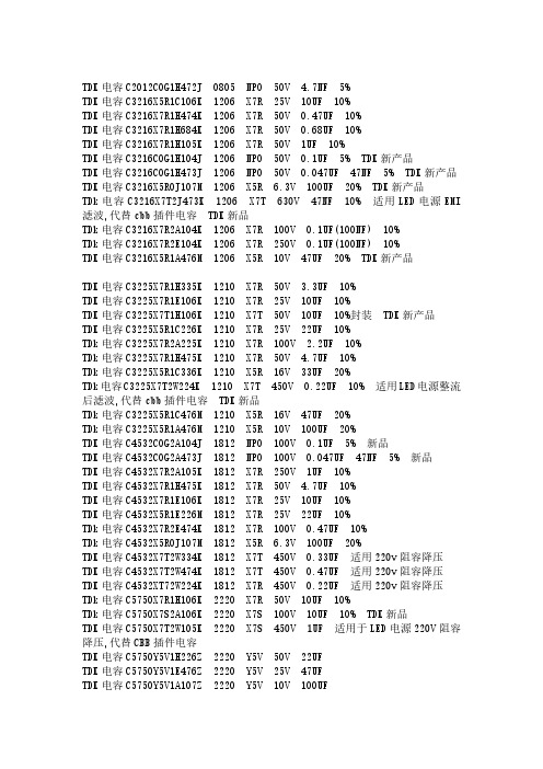
TDK电容C2012C0G1H472J0805NPO50V 4.7NF5%TDK电容C3216X5R1C106K1206X7R25V10UF10%TDK电容C3216X7R1H474K1206X7R50V0.47UF10%TDK电容C3216X7R1H684K1206X7R50V0.68UF10%TDK电容C3216X7R1H105K1206X7R50V1UF10%TDK电容C3216COG1H104J1206NPO50V0.1UF5%TDK新产品TDK电容C3216COG1H473J1206NPO50V0.047UF47NF5%TDK新产品TDK电容C3216X5R0J107M1206X5R 6.3V100UF20%TDK新产品TDk电容C3216X7T2J473K1206X7T630V47NF10%适用LED电源EMI 滤波,代替cbb插件电容TDK新品TDk电容C3216X7R2A104K1206X7R100V0.1UF(100NF)10%TDk电容C3216X7R2E104K1206X7R250V0.1UF(100NF)10%TDK电容C3216X5R1A476M1206X5R10V47UF20%TDK新产品TDK电容C3225X7R1H335K1210X7R50V 3.3UF10%TDK电容C3225X7R1E106K1210X7R25V10UF10%TDK电容C3225X7T1H106K1210X7T50V10UF10%封装TDK新产品TDK电容C3225X5R1C226K1210X7R25V22UF10%TDk电容C3225X7R2A225K1210X7R100V 2.2UF10%TDk电容C3225X7R1H475K1210X7R50V 4.7UF10%TDk电容C3225X5R1C336K1210X5R16V33UF20%TDk电容C3225X7T2W224K1210X7T450V0.22UF10%适用LED电源整流后滤波,代替cbb插件电容TDK新品TDk电容C3225X5R1C476M1210X5R16V47UF20%TDk电容C3225X5R1A476M1210X5R10V100UF20%TDK电容C4532COG2A104J1812NPO100V0.1UF5%新品TDK电容C4532COG2A473J1812NPO100V0.047UF47NF5%新品TDK电容C4532X7R2A105K1812X7R250V1UF10%TDK电容C4532X7R1H475K1812X7R50V 4.7UF10%TDK电容C4532X7R1E106K1812X7R25V10UF10%TDK电容C4532X5R1E226M1812X7R25V22UF10%TDk电容C4532X7R2E474K1812X7R100V0.47UF10%TDk电容C4532X5R0J107M1812X5R 6.3V100UF20%TDK电容C4532X7T2W334K1812X7T450V0.33UF适用220v阻容降压TDK电容C4532X7T2W474K1812X7T450V0.47UF适用220v阻容降压TDK电容C4532XT72W224K1812X7R450V0.22UF适用220v阻容降压TDk电容C5750X7R1H106K2220X7R50V10UF10%TDk电容C5750X7S2A106K2220X7S100V10UF10%TDK新品TDK电容C5750X7T2W105K2220X7S450V1UF适用于LED电源220V阻容降压,代替CBB插件电容TDK电容C5750Y5V1H226Z2220Y5V50V22UFTDK电容C5750Y5V1E476Z2220Y5V25V47UFTDK电容C5750Y5V1A107Z2220Y5V10V100UFTDK电容C5750Y5V1C107Z2220Y5V16V100UFTDK电容C5750X5R1A107M2220X5R10V100UFTDK电容C5750X5R0J107M2220X5R16V100UFTDK电容C5750X5R1A686M2220X5R10V68UFTDK电容C5750X5R1C336M2220X5R16V33UFTDK电容C5750X5R1E226M2220X5R25V22UFTDK电容C5750X5R1H106K2220X5R50V10UFTDK电容C5750X7R1C476M2220X7R16V47UFTDK电容C5750X7R1E226M2220X7R25V15UFTDK电容C5750X7R1E156M2220X7R25V 4.7UFTDK电容C5750X7R1H475K2220X7R50V 4.7UFTDK电容C5750X7R1H685K2220X7R50V 6.8UFTDK电容C5750X7R1H685M2220X7R50V 6.8UF20%TDK电容C5750X7R1H106M2220X7R50V10UF20%TDK电容C5750X7T2W684K2220X7T450V0.68UFTDK电容C5750X7R2E684K2220X7R250V0.68UFTDK电容C5750X7R2A105K2220X7R100V1UFTDK电容C5750X7T2J474K2220X7T630V0.47UFTDK电容C5750X7R2E474K2220X7R250V0.47UFTDK电容C5750X7R2A225M2220X7R100V 2.2UFTDK电容C5750X7R2A475K2220X7R100V 4.7UFTDK电容C5750X7R2A475M2220X7R100V 4.7U20%TDK电容C5750X7S2A685K2220X7S100V 6.8UF孙先生136********qq2877735032TDK共模电感(滤波器)ACM2012-900-2P-T002TDK原装新货TDK共模电感(滤波器)ACM7060-701-2PL-TL01TDK原装新货TDK贴片功率电感NLCV32T-2R2M-PF TDK原装新货TDK贴片功率电感NL453232T-102J-PF TDK原装新货TDK电感SLF6045T-1R5N4R0-3PFTDK电感SLF6045T-1R5N4R0-3PFTDK电感SLF6045T-2R2N3R3-3PFTDK电感SLF6045T-3R3N2R8-3PFTDK电感SLF6045T-4R7N2R4-3PFTDK电感SLF6045T-6R8N2R0-3PFTDK电感SLF6045T-100M1R6-3PFTDK电感SLF6045T-150M1R3-3PFTDK电感SLF6045T-220M1R1-3PFTDK电感VLCF4020T-100MR85TDK蜂鸣器PS1240P02CT3TDK-PS1240P02BT-蜂鸣器压电型70dB12.2MM制造商:TDK库存编号:制TDK蜂鸣器PS1240P02BT造商编号:PS1240P02BT输出音调类型:Low Frequency谐振频率:4kHz声压级SPL:70dB功能:Buzzer外径:12.2mm外部深度:6.5mm输出音调类型:Low Frequency谐振频率:4kHz声压级SPL:70dB功能:Buzzer外径:12.2mm外部深度:6.5mm详情咨询电话:1.利用贴片陶瓷电容器介质层的薄层化和多层叠层技术,使电容值大为扩大2.单片结构保证有极佳的机械性强度及可靠性3.极高的精确度,在进行自动装配时有高度的准确性4.因仅有陶瓷和金属构成,故即便在高温,低温环境下亦无渐衰的现象出现,具有较强可靠性与稳定性5.低集散电容的特性可完成接近理论值的电路设计6.残留诱导系数小,确保上佳的频率特性7.因电解电容器领域也获得了电容,故使用寿命延长,更造于具有高可靠性的电源8.由于esr低,频率特性良好,故最适合于高频,高密度类型的电源工作温度范围:-55~125℃额定电压:100vdc~3000vdc温度特性:npo:≤±30ppm/℃,-55~125℃(eia class i)x7r:≤±15%,-55~125℃(eia class ii)容量范围:npo:2pf to100nf;x7r:150pf to 2.2uf损失角正切(tanδ):npo:q≥1000;x7r:d.f.≤2.5%绝缘电阻:10gω或500/cω取两者最小值老化速率:npo:1%;x7r:2.5%一个decade时间日本tdk一级代理供应高频贴片电容,无线充电器专用,日本原装进口,大量现货,欢迎来电详询。
真空干燥箱
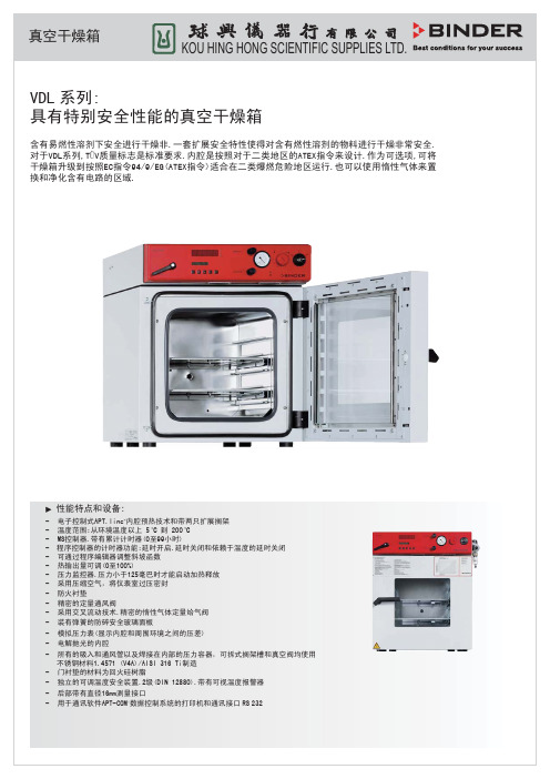
性能特点和设备:
- 电子控制式APT.line®内腔预热技术和带两只扩展搁架 - 温度范围:从环境温度以上 5 ° 到 200 ° C C - MS控制器,带有累计计时器(0至99小时) - 程序控制器的计时器功能:延时开启,延时关闭和依赖于温度的延时关闭 - 可通过程序编辑器调整斜坡函数 - 热输出量可调(0至100%) - 压力监控器,压力小于125毫巴时才能启动加热释放 - 采用压缩空气,将仪表室过压密封 - 防火衬垫 - 精密的定量通风阀 - 采用交叉流动技术,精密的惰性气体定量给气阀 - 装有弹簧的防碎安全玻璃面板 - 模拟压力表(显示内腔和周围环境之间的压差) - 电解抛光的内腔 - 所有的吸入和通风管以及焊接在内部的压力容器,可拆式搁架槽和真空阀均使用 不锈钢材料1.4571 (V4A)/AISI 316 Ti制造 - 门衬垫的材料为回火硅树脂 - 独立的可调温度安全装置,2级(DIN 12880),带有可视温度报警器 - 后部带有直径16mm测量接口 - 用于通讯软件APT-COM®数据控制系统的打印机和通讯接口 RS 232
VDL系列的技术规格
KOU HING HONG SCIENTIFIC SUPPLIES LTD.
VDL 23 外部尺寸 宽度VDL或真空模组(毫米/英寸) 高度(包括小脚)(毫米/英寸) 高度选项真空模组(毫米/英寸) 总高度VD及真空模组(毫米/英寸) 深度VDL或真空模组(毫米/英寸) 包括门把手,连接器(毫米/英寸) 后部与墙壁间隔 (毫米/英寸) 侧面与墙壁间隔 (毫米/英寸) 内部尺寸 宽度(毫米/英寸) 高度(毫米/英寸) 深度(毫米/英寸) 内膛容积(公升/立方英尺) 置物层架(铝制)(标准/最多) 层架之间距离(毫米/英寸) 层架可用空间(宽x深)(毫米/英寸) 每层架负荷重量(公斤/磅) 总承载重量(公斤/磅) 净重(空置)(公斤/磅) 温度数据 温度范围, 环境温度以上5 ° ° C到( C) 温度偏差1) 在 100 ° (± ° C C) 在 200 ° (± ° C C) 温度波动范围 (±° C) 升温时间1),2) 至 100 ° (分钟) C 至 200 ° (分钟) C 真空连接端口小型法兰管(DN毫米/英寸) 测量存取瑞口小型法兰管(DN毫米/英寸 惰性气体通气管接口,备各有控流量器-线 (RP”) 惰性气体通气管接口,备各有控流量器 备有Hose Olive接管的调制器(DN毫米/英寸) 最大真空度(bar/torr) 泄漏比率 (最高 mbar 每小时 / torr 每小时) 压缩空气接口直径 (毫米/英寸) 压缩空气流量 (升/分钟) 电气数据 箱体保护 (依照 EN60529) 额定电压 (±10 %) 50/60 Hz (V) 额定功率 (W) 耗电量 当 100 ° (W) C 当 200 ° (W) C
初期干燥抗裂试验仪的参数介绍
初期干燥抗裂试验仪的参数介绍
初期干燥抗裂试验仪用于复层建筑涂料初期干燥抗开裂性能的测定,该仪器采用轴流风机送风,风机可无级调速。
适用于GB/T9779-1988标准。
初期干燥抗裂试验仪设备仪器:
试板架和风量调节装置。
计时器。
风速计。
轴流风机。
试验风洞。
初期干燥抗裂试验仪参数:
仪器总功率:l00w。
风机风速:3米/秒±0.3(可无级调速)。
风速仪:O~10米/秒。
外形尺寸:主机1000x30Ox360mm(长x宽x高)控制器240x210Xll0mm(长X宽X 高)。
整机重量:27Kg。
工作原理:
电机通过齿轮减速后拖动顶杆作上升运动,刃口产生上顶力,使石棉水泥板在规定的区域内逐步产生细微裂纹并控制裂纹缓慢扩展,观察腻子层的开裂情况,以此表征腻子抵抗基材裂纹扩展的能力。
结果判断:
三块试板中以数值较近的每块试板的测试结果的算术平均值作为zui终结果。
标签:
初期干燥抗裂试验仪。
- 1、下载文档前请自行甄别文档内容的完整性,平台不提供额外的编辑、内容补充、找答案等附加服务。
- 2、"仅部分预览"的文档,不可在线预览部分如存在完整性等问题,可反馈申请退款(可完整预览的文档不适用该条件!)。
- 3、如文档侵犯您的权益,请联系客服反馈,我们会尽快为您处理(人工客服工作时间:9:00-18:30)。
元器件交易网
元器件交易网
元器件交易网
元器件交易网
元器件交易网
元器件交易网
元器件交易网
元器件交易网
元器件交易网
元器件交易网
元器件交易网
元器件交易网
元器件交易网
元器件交易网
元器件交易网
元器件交易网
元器件交易网
元器件交易网
元器件交易网www.ceபைடு நூலகம்
元器件交易网
元器件交易网
元器件交易网
元器件交易网
元器件交易网
元器件交易网
元器件交易网
元器件交易网
元器件交易网
元器件交易网
元器件交易网
元器件交易网
元器件交易网
元器件交易网
元器件交易网
元器件交易网
元器件交易网
元器件交易网
元器件交易网
元器件交易网
元器件交易网
