UGN3177LTTR中文资料
LM317T应用电路及其资料

/p-54101912.html
LM317中文资料
LM117/LM317 是美国国家半导体公司的三端可调正稳压器集成电路。
LM117/LM317 的输出电压范围是1.2V至37V,负载电流最大为1.5A。
它的使用非常简单,仅需两个外接电阻来设置输出电压。
此外它的线性调整率和负载调整率也比标准的固定稳压器好。
LM117/LM317 内置有过载保护、安全区保护等多种保护电路。
通常 LM117/LM317 不需要外接电容,除非输入滤波电容到
LM117/LM317 输入端的连线超过 6 英寸(约 15 厘米)。
使用输出电容能改变瞬态响应。
调整端使用滤波电容能得到比标准三端稳压器高的多的纹波抑制比。
LM117/LM317能够有许多特殊的用法。
比如把调整端悬浮到一个较高的电压上,可以用来调节高达数百伏的电压,只要输入输出压差不超过LM117/LM317的极限就行。
当然还要避免输出端短路。
还可以把调整端接到一个可编程电压上,实现可编程的电源输出。
特性简介
可调整输出电压低到1.2V。
保证1.5A 输出电流。
典型线性调整率0.01%。
典型负载调整率0.1%。
80dB 纹波抑制比。
输出短路保护。
过流、过热保护。
调整管安全工作区保护。
标准三端晶体管封装。
电压范围
LM117/LM317 1.25V 至 37V 连续可调。
其封装形式如下:。
LM317中英文资料
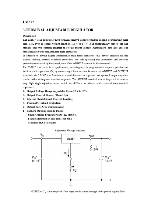
LM3173-TERMINAL ADJUSTABLE REGULATORDescriptionThe LM317 is an adjustable three-terminal positive-voltage regulator capable of supplying more than 1.5A over an output-voltage range of 1.2 V to 37 V. It is exceptionally easy to use and requires only two external resistors to set the output voltage. Furthermore, both line and load regulation are better than standard fixed regulators.In addition to having higher performance than fixed regulators, this device includes on-chip current limiting, thermal overload protection, and safe-operating-area protection. All overload protection remains fully functional, even if the ADJUST terminal is disconnected.The LM317 is versatile in its applications, including uses in programmable output regulation and local on-card regulation. Or, by connecting a fixed resistor between the ADJUST and OUTPUT terminals, the LM317 can function as a precision current regulator. An optional output capacitor can be added to improve transient response. The ADJUST terminal can be bypassed to achieve very high ripple-rejection ratios, which are difficult to achieve with standard three-terminal regulators.1、Output Voltage Range Adjustable From1.2 V to 37 V2、Output Current Greater Than 1.5 A3、Internal Short-Circuit Current Limiting4、Thermal Overload Protection5、Output Safe-Area Compensation6、Package Options Include PlasticSmall-Outline Transistor SOT-223 (DCY),Flange Mounted (KTE) and Heat-SinkMounted (KC) PackagesAdjustable V oltage regulatorNOTES:A.Cis not required if the regulator is closed enough to the power-supply filter.inB.Coimproves transient response, but is not needed for stability.Vout is calculated as Vout=Vref(1+12RR)+(IAdj×R2)APPLICATION INFORMATIONBasic Circuit OperationThe LM317 is a 3−terminal floating regulator. In operation, the LM317 develops and maintains a nominal 1.25 V reference (Vref) between its output and adjustment terminals. This reference voltage is converted to a programming current (IPROG) by R1 (see Figure 17), and this constant current flows through R2 to ground. The regulated output voltage is given by:Vout =Vref(1+12RR)+(IAdj×R2)Since the current from the adjustment terminal (IAdj) represents an error term in the equation, theLM317 was designed to control IAdjto less than 100 A and keep it constant. To do this, all quiescent operating current is returned to the output terminal. This imposes the requirement for a minimum load current. If the load current is less than this minimum, the output voltage will rise. Since the LM317 is a floating regulator, it is only the voltage differential across the circuit which is important to performance, and operation at high voltages with respect to ground is possible.Basic Circuit ConfigurationVref=1.25V TypicalLoad RegulationThe LM317 is capable of providing extremely good load regulation, but a few precautions are needed to obtain maximum performance. For best performance, the programming resistor (R1) should be connected as close to the regulator as possible to minimize line drops which effectively appear in series with the reference, thereby degrading regulation. The ground end of R2 can be returned near the load ground to provide remote ground sensing and improve load regulation.External CapacitorsA 0.1 μF disc or 1.0 μF tantalum input bypass capacitor (Cin) is recommended to reduce the sensitivity to input line impedance. The adjustment terminal may be bypassed to ground toimprove ripple rejection. This capacitor (CAdj) prevents ripple from being amplified as the output voltage is increased. A 10 μF capacitor should improve ripple rejection about 15 dB at 120 Hz in a 10 V application. Although the LM317 is stable with no output capacitance, like any feedback circuit, certain values of external capacitance can cause excessive ringing. An output capacitance(Co) in the form of a 1.0 μF tantalum or 25 μF aluminum electrolytic capacitor on the output swamps this effect and insures stability.Protection DiodesWhen external capacitors are used with any IC regulator it is sometimes necessary to add protection diodes to prevent the capacitors from discharging through low current points into the regulator. Figure 18 shows the LM317 with the recommended protection diodes for outputvoltages in excess of 25 V or high capacitance values (Co > 25 μF, CAdj> 10 μF). Diode D1prevents Cofrom discharging thru the IC during an input short circuit. Diode D2 protects againstcapacitor CAdjdischarging through the IC during an output short circuit. The combination ofdiodes D1 and D2 prevents CAdjfrom discharging through the IC during an input short circuit. Voltage Regulator with Protection DiodesLM317—三端可调节输出正电压稳压器概述LM317是3端可调节输出正电压稳压器,在输出范围为1.2V到37V范围时能提供超过1.5A的电流。
TL317中文资料

元器件交易网IMPORTANT NOTICETexas Instruments and its subsidiaries (TI) reserve the right to make changes to their products or to discontinueany product or service without notice, and advise customers to obtain the latest version of relevant informationto verify, before placing orders, that information being relied on is current and complete. All products are soldsubject to the terms and conditions of sale supplied at the time of order acknowledgement, including thosepertaining to warranty, patent infringement, and limitation of liability.TI warrants performance of its semiconductor products to the specifications applicable at the time of sale inaccordance with TI’s standard warranty. Testing and other quality control techniques are utilized to the extentTI deems necessary to support this warranty. Specific testing of all parameters of each device is not necessarilyperformed, except those mandated by government requirements.CERTAIN APPLICATIONS USING SEMICONDUCTOR PRODUCTS MAY INVOLVE POTENTIAL RISKS OFDEATH, PERSONAL INJURY, OR SEVERE PROPERTY OR ENVIRONMENTAL DAMAGE (“CRITICALAPPLICATIONS”). TI SEMICONDUCTOR PRODUCTS ARE NOT DESIGNED, AUTHORIZED, ORWARRANTED TO BE SUITABLE FOR USE IN LIFE-SUPPORT DEVICES OR SYSTEMS OR OTHERCRITICAL APPLICATIONS. INCLUSION OF TI PRODUCTS IN SUCH APPLICATIONS IS UNDERSTOOD TOBE FULLY AT THE CUSTOMER’S RISK.In order to minimize risks associated with the customer’s applications, adequate design and operatingsafeguards must be provided by the customer to minimize inherent or procedural hazards.TI assumes no liability for applications assistance or customer product design. TI does not warrant or representthat any license, either express or implied, is granted under any patent right, copyright, mask work right, or otherintellectual property right of TI covering or relating to any combination, machine, or process in which suchsemiconductor products or services might be or are used. TI’s publication of information regarding any thirdparty’s products or services does not constitute TI’s approval, warranty or endorsement thereof.Copyright © 1999, Texas Instruments Incorporated。
lm317中文资料及应用

LM317中文资料LM117/LM317 是美国国家半导体公司的三端可调正稳压器集成电路。
LM117/LM317 的输出电压范围是1.2V至37V,负载电流最大为1.5A。
它的使用非常简单,仅需两个外接电阻来设置输出电压。
此外它的线性调整率和负载调整率也比标准的固定稳压器好。
LM117/LM317 内置有过载保护、安全区保护等多种保护电路。
通常 LM117/LM317 不需要外接电容,除非输入滤波电容到LM117/LM317 输入端的连线超过 6 英寸(约 15 厘米)。
使用输出电容能改变瞬态响应。
调整端使用滤波电容能得到比标准三端稳压器高的多的纹波抑制比。
LM117/LM317能够有许多特殊的用法。
比如把调整端悬浮到一个较高的电压上,可以用来调节高达数百伏的电压,只要输入输出压差不超过LM117/LM317的极限就行。
当然还要避免输出端短路。
还可以把调整端接到一个可编程电压上,实现可编程的电源输出。
特性简介可调整输出电压低到1.2V。
保证1.5A 输出电流。
典型线性调整率0.01%。
典型负载调整率0.1%。
80dB 纹波抑制比。
输出短路保护。
过流、过热保护。
调整管安全工作区保护。
标准三端晶体管封装。
电压范围LM117/LM317 1.25V 至 37V 连续可调。
其封装形式如下:绝对最大额定值符号参数值单位VI-O 输入-输出电压差40 VIO 输出电流内部限制Top 工作结温LM117 -55到150 ℃LM217 -25到150LM317 0到125Ptot 功耗内部限制Tstg 储存温度-65到150 ℃LM317工作原理:LM317的输入最同电压为30多伏,输出电压1.5----32V...电流1.5A...不过在用的时候要注意功耗问题...注意散热问题。
LM317有三个引脚.一个输入一个输出一个电压调节。
输入引脚输入正电压,输出引脚接负载, 电压调节引脚一个引脚接电阻(200左右)在输出引脚,另一个接可调电阻(几K)接于地.输入和输出引脚对地要接滤波电容.LM317内部原理图:LM317应用电路图:1.LM317标准应用电路图2.LM317带可调限流和输出电压的标准应用电路图3. LM317的5.0V电子关断稳压器应用电路图4.LM317电流稳压器应用电路图5.LM317可调节电流限流器的应用电路图6. LM317软启动应用电路图图1 基本的LM317稳压电源电路正电压输出型图2 基本的LM337稳压电源电路负电压输出型图3 完整的LM317稳压电源电路正电压输出型LM317输出电流为1.5A,输出电压可在1.25-37V之间连续调节,其输出电压由两只外接电阻R1、 RP1决定,输出端和调整端之间的电压差为1.25V,这个电压将产生几毫安的电流,经R1、RP1到地,在RP1上分得的电压加到调整端,通过改变 RP1就能改变输出电压。
三端可调节输出正电压稳压器LM317T资料
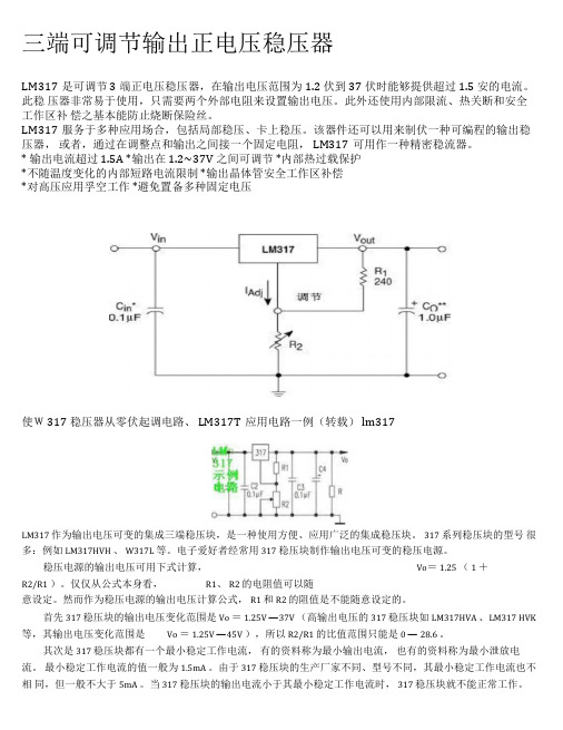
三端可调节输出正电压稳压器LM317是可调节3 端正电压稳压器,在输出电压范围为1.2 伏到37 伏时能够提供超过1.5 安的电流。
此稳压器非常易于使用,只需要两个外部电阻来设置输出电压。
此外还使用内部限流、热关断和安全工作区补偿之基本能防止烧断保险丝。
LM317服务于多种应用场合,包括局部稳压、卡上稳压。
该器件还可以用来制伏一种可编程的输出稳压器,或者,通过在调整点和输出之间接一个固定电阻,LM317可用作一种精密稳流器。
* 输出电流超过1.5A *输出在1.2~37V 之间可调节*内部热过载保护*不随温度变化的内部短路电流限制*输出晶体管安全工作区补偿*对高压应用孚空工作*避免置备多种固定电压使W317 稳压器从零伏起调电路、LM317T应用电路一例(转载)lm317LM317 作为输出电压可变的集成三端稳压块,是一种使用方便、应用广泛的集成稳压块。
317 系列稳压块的型号很多:例如LM317HVH 、W317L 等。
电子爱好者经常用317 稳压块制作输出电压可变的稳压电源。
稳压电源的输出电压可用下式计算,Vo=1.25 (1 +R2/R1 )。
仅仅从公式本身看,R1、R2 的电阻值可以随意设定。
然而作为稳压电源的输出电压计算公式,R1 和R2 的阻值是不能随意设定的。
首先317 稳压块的输出电压变化范围是Vo =1.25V —37V (高输出电压的317 稳压块如LM317HVA 、LM317 HVK 等,其输出电压变化范围是Vo =1.25V —45V ),所以R2/R1 的比值范围只能是0 —28.6 。
其次是317 稳压块都有一个最小稳定工作电流,有的资料称为最小输出电流,也有的资料称为最小泄放电流。
最小稳定工作电流的值一般为1.5mA 。
由于317 稳压块的生产厂家不同、型号不同,其最小稳定工作电流也不相同,但一般不大于5mA 。
当317 稳压块的输出电流小于其最小稳定工作电流时,317 稳压块就不能正常工作。
lm317中文资料及应用

lm317中文资料及应用LM317中文资料LM117/LM317 是美国国家半导体公司的三端可调正稳压器集成电路。
LM117/LM317 的输出电压范围是1.2V至37V,负载电流最大为1.5A。
它的使用非常简单,仅需两个外接电阻来设置输出电压。
此外它的线性调整率和负载调整率也比标准的固定稳压器好。
LM117/LM317 内置有过载保护、安全区保护等多种保护电路。
通常 LM117/LM317 不需要外接电容,除非输入滤波电容到 LM117/LM317 输入端的连线超过 6 英寸(约 15 厘米)。
使用输出电容能改变瞬态响应。
调整端使用滤波电容能得到比标准三端稳压器高的多的纹波抑制比。
LM117/LM317能够有许多特殊的用法。
比如把调整端悬浮到一个较高的电压上,可以用来调节高达数百伏的电压,只要输入输出压差不超过LM117/LM317的极限就行。
当然还要避免输出端短路。
还可以把调整端接到一个可编程电压上,实现可编程的电源输出。
特性简介可调整输出电压低到1.2V。
保证1.5A 输出电流。
典型线性调整率0.01%。
典型负载调整率0.1%。
80dB 纹波抑制比。
输出短路保护。
过流、过热保护。
调整管安全工作区保护。
标准三端晶体管封装。
电压范围LM117/LM317 1.25V 至 37V 连续可调。
其封装形式如下:绝对最大额定值符号参数值单位输入,输出电压VI-O 40 V 差IO 输出电流内部限制Top 工作结温 LM117 -55到150 ?LM217 -25到150LM317 0到125Ptot 功耗内部限制Tstg 储存温度 -65到150 ?LM317工作原理:LM317的输入最同电压为30多伏,输出电压1.5----32V...电流1.5A...不过在用的时候要注意功耗问题...注意散热问题。
LM317有三个引脚.一个输入一个输出一个电压调节。
输入引脚输入正电压,输出引脚接负载, 电压调节引脚一个引脚接电阻(200左右)在输出引脚,另一个接可调电阻(几K)接于地.输入和输出引脚对地要接滤波电容.LM317内部原理图:LM317应用电路图:1.LM317标准应用电路图2.LM317带可调限流和输出电压的标准应用电路图3. LM317的5.0V电子关断稳压器应用电路图4.LM317电流稳压器应用电路图5.LM317可调节电流限流器的应用电路图6. LM317软启动应用电路图图1 基本的LM317稳压电源电路正电压输出型图2 基本的LM337稳压电源电路负电压输出型图3 完整的LM317稳压电源电路正电压输出型LM317输出电流为1.5A,输出电压可在1.25,37V之间连续调节,其输出电压由两只外接电阻R1、 RP1决定,输出端和调整端之间的电压差为1.25V,这个电压将产生几毫安的电流,经R1、RP1到地,在RP1上分得的电压加到调整端,通过改变 RP1就能改变输出电压。
LM317T中文资料_数据手册_参数
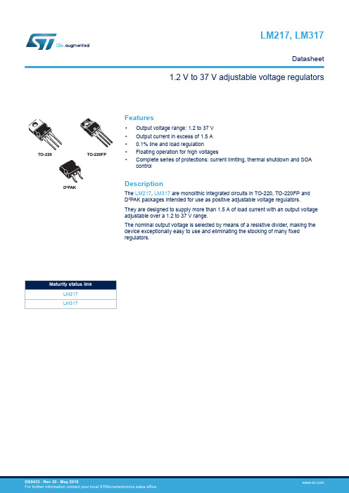
Description
The LM217, LM317 are monolithic integrated circuits in TO-220, TO-220FP and D²PAK packages intended for use as positive adjustable voltage regulators.
1.5 2.2 A
0.4
eN
Output noise voltage (percentage of VO)
B = 10 Hz to 100 kHz, TJ = 25°C
0.003
%
SVR
Supply voltage rejection (1)
CADJ = 0
65
TJ = 25°C, f = 120 Hz
0.02 0.07
ΔVO
Load regulation
VO ≤ 5 V IO = 10 mA to IMAX
VO ≥ 5 V, IO = 10 mA to IMAX
TJ= 25°C TJ = 25°C
5 25 mV
20 70 0.1 0.5
% 0.3 1.5
IADJ
Adjustment pin current
Table 4. Electrical characteristics for LM317
Symbol
Parameter
Test conditions
Min. Typ. Max. Unit
ΔVO
Line regulation
VI - VO = 3 to 40 V
TJ = 25°C
0.01 0.04 %/V
Maturity status link LM217 LM317
lm317工作原理

lm317工作原理
LM317是一种电流稳压器,采用了可调输出电压的线性稳压
器电路。
它具有广泛的应用领域,特别是在电子设备中常被用作电源稳压器。
其工作原理是通过调节输出电压与调节电阻之间的关系来实现稳压输出。
它的输入端通过一个截止电容和一个电源电阻与输入电源相连,输出端则连接到负载电阻上。
通过调节电阻的大小,可以改变输入端和输出端之间的电位差,从而达到稳压的效果。
在LM317内部,有一个参考电压源,其电位差为1.25V。
在
电路中的调节电阻通过改变输出电压和参考电压之间的电流差,以调整输出电压的大小。
当调节电阻减小时,输出电压将增加;反之,当调节电阻增加时,输出电压将减小。
为了保证稳定的输出电压,LM317还通过集电极电流(输出
电流)和输出电阻来进行反馈。
这使得输出电压的变化对输入电压的变化不敏感,从而实现稳定的输出。
需要注意的是,为了保证正常工作,LM317的工作电流应大
于最小负载电流,否则可能会导致输出电压不稳定。
此外,还需要合理选择输入电源和散热器,以确保LM317能正常工作
并避免过热。
总之,LM317通过调节输出电压与调节电阻之间的关系,以
及反馈机制来实现稳压输出。
它是一种常用的线性稳压器电路,广泛应用于各类电子设备中。
UTCLM317L

U T C LM317L LINEAR INTEGRATED CIRCUITUTC UNISONIC TECHNOLOGIES CO., LTD.1QW-R101-008,ALOW CURRENT 1.25V TO 37V ADJUSTABLE VOLTAGE REGULATORDESCRIPTIONThe UTC LM317L is a monolithic integrated circuit, designed for use as positive adjustable voltage regulator. It is designed to supply until 100mA of load current with an output voltage adjustable over a 1.25V to 37V range.FEATURES*Output voltage range: 1.25V to 37V *Output current in excess of 100mA *Line regulation typ. 0.01%*Load regulation typ. 0.1%*Thermal overload protection *Short circuit protection*Output transistor safe area compensation*Floating operation for high voltage applicationsPIN CONFIGURATIONS12348765NC V OUTV OUT V INUTC LM317LADJV OUTV OUTNCTO-92 Plastic PackageBottom ViewSOP-8 PACKAGEABSOLUTE MAXIMUM RATINGPARAMETERSYMBOL VALUE UNIT Input-Output Differential Voltage Vi-Vo 40V Power DissipationPd Internally LimitedOperating Junction Temperature Range Topr 0~125°C Storage Temperature RangeTstr-55 ~ 150°CU T C LM317L LINEAR INTEGRATED CIRCUITUTC UNISONIC TECHNOLOGIES CO., LTD.2QW-R101-008,ASCHEMATIC DIAGRAMTEST CIRCUITOUTPUT INPUTADJUSTU T C LM317L LINEAR INTEGRATED CIRCUITUTC UNISONIC TECHNOLOGIES CO., LTD.3QW-R101-008,AELECTRICAL CHARACTERISTICS (Vi-Vo=5V, Io=40mA, 0<=Tj<=125°C, unless otherwise specified)PARAMETER SYMBOL TEST CONDITIONS MIN TYP MAXUNIT Line Regulation ∆Vo Vi-Vo=3~40V I L <20mATj=25°C 0.010. 04%/V 0.020.07%/V Load Regulation∆VoVo<=5VIo=5~100mA Tj=25°C525mV 2070mV Vo>=5V Io=5~100mATj=25°C0.10.5%0.3 1.5%Adjustment Pin Current I ADJ 50100µA Adjustment Pin Current ∆I ADJ Vi-Vo=3~40VIo=5~100mA, Pd< 625 mW0.25µA Reference VoltageV REF Vi-Vo=3~40VIo=5~100 mA , Pd< 625 mW 1.21.25 1.3V Output Voltage Temperature Stability∆Vo/Vo 0.7%Minimum Load Current Io(min)Vi-Vo=40V 3.55mA Maximum Output CurrentIo(max)Vi-Vo=3~13V Vi-Vo=40V 10020050mA Output Noise Voltage (Percentance of Vo)eN B=10Hz~10KHzTj=25°C0.003%Supply Voltage Rejection(*)SVRTj=25°C f=120HzC ADJ =065dB C ADJ =10µF6680dB(*) CADJ is connected between Adjust pin and Ground.100200300I 0(mA)N OUT (V)CURRENT LIMIT I 0(mA)N OUT (V)MINIMUM OPERATING CURRENT0.51.01.52.02.53.0U T C LM317L LINEAR INTEGRATED CIRCUIT APPLICATION INFORMATIONThe UTC LM317L provides an internal reference voltage of 1.25V between the output and adjustments terminals. This is used to set a constant current flow across an external resistor divider, giving an output voltage VO of:VO=V REF (1+R2/R1) + I ADJ R2The device is designed to minimize the term I ADJ (100µA max) and to maintain it very constant with line and load changes. Usually, the error term IADJ. R2 can be neglected. To obtain the previous requirement, all the regulator quiescent current is returned to the output terminal, imposing a minimum load current condition. If the load is insufficient, the output voltage will rise. The UTC LM317L is a floating regulator, input-output differential voltage, supplies of very high voltage with respect to ground can be regulated as long as the maximum input-output differential is not exceeded. Furthermore, programmable regulators are easily obtainable and, by connecting a fixed resistor between the adjustment and output, the device can be used as a precision current regulator.UTC UNISONIC TECHNOLOGIES CO., LTD.4QW-R101-008,AU T C LM317L LINEAR INTEGRATED CIRCUITUTC UNISONIC TECHNOLOGIES CO., LTD.5QW-R101-008,AIo=Vref R1+I ADJ ≅1.25V R1DIGITAL INPUTS(R2 sets maximun Vo)DIGITALLY SELECTED OUTPUTSCURRENT REGULATORSLOW TURN-ON 15V REGULATOR5V ELECTRONIC SHUT-DOWN REGULATORVOLTAGE REGULATOR WITH PROTECTION DIODES。
LM317LDR2中文资料
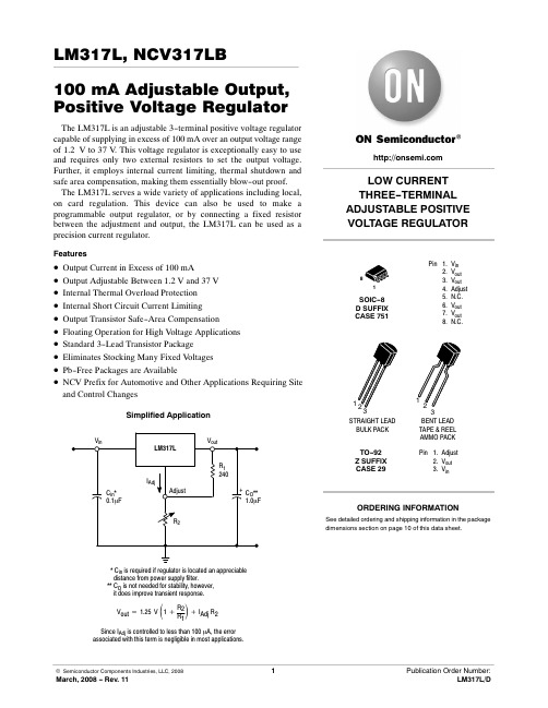
4
RR
dB
60
80
-
-
80
-
-
-
-
180
-
°C
Long Term Stability, TJ = Thigh (Note 8) TA = 25°C for Endpoint Measurements
3
S
-
0.3
1.0
%/1.0 k
Hrs.
3. Tlow to Thigh = 0° to +125°C for LM317L -40° to +125°C for LM317LB, NCV317LB 4. Imax = 100 mAąąPmax = 625 mW 5. Load and line regulation are specified at constant junction temperature. Changes in VO due to heating effects must be taken into account
1
Regline
-
0.02
0.07
%/V
Load Regulation (Note 5)
ą10 mA ≤ IO ≤ Imax - LM317L ąąVO ≤ 5.0 V ąąVO ≥ 5.0 V
2
Regload
-
20
70
mV
0.3
1.5
% VO
Temperature Stability (Tlow ≤ TJ ≤ Thigh)
Vin
300
300
300
3.0k 300
70
lm317中文资料
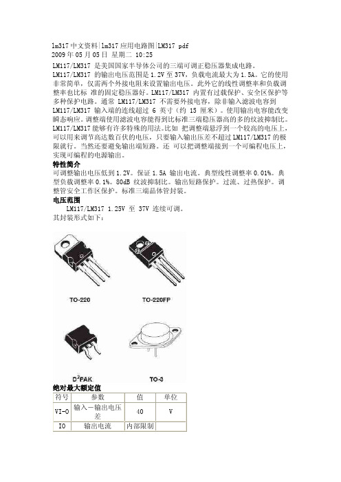
lm317中文资料|lm317应用电路图|LM317 pdf2009年05月05日 星期二 10:25LM117/LM317 是美国国家半导体公司的三端可调正稳压器集成电路。
LM117/LM317 的输出电压范围是1.2V至37V,负载电流最大为1.5A。
它的使用非常简单,仅需两个外接电阻来设置输出电压。
此外它的线性调整率和负载调整率也比标 准的固定稳压器好。
LM117/LM317 内置有过载保护、安全区保护等多种保护电路。
通常 LM117/LM317 不需要外接电容,除非输入滤波电容到LM117/LM317 输入端的连线超过 6 英寸(约 15 厘米)。
使用输出电容能改变瞬态响应。
调整端使用滤波电容能得到比标准三端稳压器高的多的纹波抑制比。
LM117/LM317能够有许多特殊的用法。
比如 把调整端悬浮到一个较高的电压上,可以用来调节高达数百伏的电压,只要输入输出压差不超过LM117/LM317的极限就行。
当然还要避免输出端短路。
还 可以把调整端接到一个可编程电压上,实现可编程的电源输出。
特性简介可调整输出电压低到1.2V。
保证1.5A 输出电流。
典型线性调整率0.01%。
典型负载调整率0.1%。
80dB 纹波抑制比。
输出短路保护。
过流、过热保护。
调整管安全工作区保护。
标准三端晶体管封装。
电压范围LM117/LM317 1.25V 至 37V 连续可调。
其封装形式如下:LM317工作原理:LM317的输入最同电压为30多伏,输出电压1.5----32V...电流1.5A...不过在用的时候要注意功耗问题...注意散热问题。
LM317有三个引脚.一个输入一个输出一个电压调节。
输入引脚输入正电压,输出引脚接负载, 电压调节引脚一个引脚接电阻(200左右)在输出引脚,另一个接可调电阻(几K)接于地.输入和输出引脚对地要接滤波电容.LM317内部原理图:LM317应用电路图:1.LM317标准应用电路图2.LM317带可调限流和输出电压的标准应用电路图3. LM317的5.0V电子关断稳压器应用电路图4.LM317电流稳压器应用电路图5.LM317可调节电流限流器的应用电路图6. LM317软启动应用电路图。
三端可调节输出正电压稳压器LM317T资料

三端可调节输出正电压稳压器LM317是可调节3 端正电压稳压器,在输出电压范围为1.2 伏到37 伏时能够提供超过1.5 安的电流。
此稳压器非常易于使用,只需要两个外部电阻来设置输出电压。
此外还使用内部限流、热关断和安全工作区补偿之基本能防止烧断保险丝。
LM317服务于多种应用场合,包括局部稳压、卡上稳压。
该器件还可以用来制伏一种可编程的输出稳压器,或者,通过在调整点和输出之间接一个固定电阻,LM317可用作一种精密稳流器。
* 输出电流超过1.5A *输出在1.2~37V 之间可调节*内部热过载保护*不随温度变化的内部短路电流限制*输出晶体管安全工作区补偿*对高压应用孚空工作*避免置备多种固定电压使W317 稳压器从零伏起调电路、LM317T应用电路一例(转载)lm317LM317 作为输出电压可变的集成三端稳压块,是一种使用方便、应用广泛的集成稳压块。
317 系列稳压块的型号很多:例如LM317HVH 、W317L 等。
电子爱好者经常用317 稳压块制作输出电压可变的稳压电源。
稳压电源的输出电压可用下式计算,Vo=1.25 (1 +R2/R1 )。
仅仅从公式本身看,R1、R2 的电阻值可以随意设定。
然而作为稳压电源的输出电压计算公式,R1 和R2 的阻值是不能随意设定的。
首先317 稳压块的输出电压变化范围是Vo =1.25V —37V (高输出电压的317 稳压块如LM317HVA 、LM317 HVK 等,其输出电压变化范围是Vo =1.25V —45V ),所以R2/R1 的比值范围只能是0 —28.6 。
其次是317 稳压块都有一个最小稳定工作电流,有的资料称为最小输出电流,也有的资料称为最小泄放电流。
最小稳定工作电流的值一般为1.5mA 。
由于317 稳压块的生产厂家不同、型号不同,其最小稳定工作电流也不相同,但一般不大于5mA 。
当317 稳压块的输出电流小于其最小稳定工作电流时,317 稳压块就不能正常工作。
LM317T中文资料

元器件交易网LM317T (KA317)LM317T (KA317)ABSOLUTE MAXIMUM RATINGS (T A = +25°C, unless otherwise speci fied)ELECTRICAL CHARACTERISTICS(V I - V O = 5V, I O = 0.5A, 0°C ≤ T J ≤ +125°C, I MAX = 1.5A, P MAX = 20W, unless otherwise specified) *Load and line regulation are specified at constant junction temperature. Change in V D due to heating effects must be taken into account separately. Pulse testing with low duty is used. (PMAX = 20W)CharacteristicSymbol Value Unit Input-Output Voltage Differential V I - V O 40V Lead T emperature T LEAD 230°C Power DissipationP D Internally limitedW Operating T emperature Range T OPR 0 ~ +125°C Storage T emperature RangeT STG -65 ~ +125°C T emperature Coef ficient of Output VoltageV O /T0.02%/°CCharacteristicSymbol Test ConditionsMinTyp Max Unit Line Regulation Rline T A = +25°C 3V ≤ V I - V O ≤ 40V0.010.04%/V 3V ≤ V I - V O ≤ 40V0.020.07%/V Load RegulationRloadT A = +25°C, 10mA ≤ I O ≤ I MAX V O < 5V V O ≥ 5V180.4250.5mV %/V O 10mA ≤ I O ≤ I MAX V O < 5V V O ≥ 5V400.8701.5mV %/V O Adjustable Pin CurrentI ADJ 46100µA Adjustable Pin Current Change∆ I ADJ3V ≤ V I - V O ≤ 40V 10mA ≤ I O ≤ I MAX P ≤ P MAX2.05µAReference VoltageV REF3V ≤ V IN - V OUT ≤ 40V 10mA ≤ I O ≤ I MAX P D ≤ P MAX 1.20 1.25 1.30VT emperature StabilityST t 0.7%/V O Minimum Load Current to Maintain RegulationL (MIN) V I - V O = 40V3.512mA Maximum Output Current I O(MAX) V I - V O ≤ 15V , P D ≤ P MAXV I - V O ≤ 40V, P D ≤ P MAX , T A = 25°C 1.0 2.20.3ARMS Noise, % of V OUT e N T A = +25°C, 10Hz ≤ f ≤ 10KHz 0.0030.01%/V O Ripple RejectionRRV O = 10V , f = 120Hz without C ADJ C ADJ = 10µF666075dBLong-Term Stability, T J = T HIGH ST T A = +25°C for end point measurements, 1000HR0.31%Thermal Resistance Junction to CaseR θ JC5°C/W元器件交易网元器件交易网LM317T (KA317)TRADEMARKSThe following are registered and unregistered trademarks Fairchild Semiconductor owns or is authorized to use and is not intended to be an exhaustive list of all such trademarks.ACEx™Bottomless™CoolFET™CROSSVOLT™E2CMOS™FACT™FACT Quiet Series™FAST®FASTr™GTO™HiSeC™ISOPLANAR™MICROWIRE™POP™PowerTrench®QFET™QS™Quiet Series™SuperSOT™-3SuperSOT™-6SuperSOT™-8SyncFET™TinyLogic™UHC™VCX™DISCLAIMERFAIRCHILD SEMICONDUCTOR RESERVES THE RIGHT TO MAKE CHANGES WITHOUT FURTHER NOTICE TO ANY PRODUCTS HEREIN TO IMPROVE RELIABILITY, FUNCTION OR DESIGN. FAIRCHILD DOES NOT ASSUME ANY LIABILITY ARISING OUT OF THE APPLICATION OR USE OF ANY PRODUCT OR CIRCUIT DESCRIBED HEREIN; NEITHER DOES IT CONVEY ANY LICENSE UNDER ITS PATENT RIGHTS, NOR THE RIGHTS OF OTHERS.LIFE SUPPORT POLICYFAIRCHILD’S PRODUCTS ARE NOT AUTHORIZED FOR USE AS CRITICAL COMPONENTS IN LIFE SUPPORT DEVICES OR SYSTEMS WITHOUT THE EXPRESS WRITTEN APPROVAL OF FAIRCHILD SEMICONDUCTOR CORPORATION.As used herein:1. Life support devices or systems are devices or systems which, (a) are intended for surgical implant into the body, or (b) support or sustain life, or (c) whose failure to perform when properly used in accordance with instructions for use provided in the labeling, can be reasonably expected to result in significant injury to the user.2. A critical component is any component of a life support device or system whose failure to perform can be reasonably expected to cause the failure of the life support device or system, or to affect its safety or effectiveness.PRODUCT STATUS DEFINITIONSDefinition of TermsDatasheet Identification Product Status DefinitionAdvance Information Formative or InDesign This datasheet contains the design specifications for product development. Specifications may change in any manner without notice.Preliminary First Production This datasheet contains preliminary data, andsupplementary data will be published at a later date.Fairchild Semiconductor reserves the right to makechanges at any time without notice in order to improvedesign.No Identification Needed Full Production This datasheet contains final specifications. FairchildSemiconductor reserves the right to make changes atany time without notice in order to improve design.Obsolete Not In Production This datasheet contains specifications on a productthat has been discontinued by Fairchild semiconductor.The datasheet is printed for reference information only.元器件交易网。
UGN3177LT中文资料

These Hall-effect latches are temperature-stable and stress-resistant sensors especially suited for electronic commutation in brushless dc motors using multipole ring magnets. Each device includes a voltage regulator, quadratic Hall voltage generator, temperature compensation circuit, signal amplifier, Schmitt trigger, and an open-collector output on a single silicon chip. The on-board regulator permits operation with supply voltages of 4.5 volts to 18 volts. The switch output can sink 10 mA. With suitable output pull up, they can be used directly with bipolar or MOS logic circuits.The three package styles available provide a magnetically optimized package for most applications. Suffix ‘LT’ is a surface-mount SOT-89/TO-243AA package; suffixes ‘U’ and ‘UA’ feature wire leads for through-hole mounting.HALL-EFFECT LATCHESAlways order by complete part number, e.g., UGN3175LT .See Magnetic Characteristics table for differences between devices.Data Sheet27609.4AFEATURESI Symmetrical Response I 4.5 V to 18 V Operation I Open-Collector Output I Reverse Battery ProtectionI Activate With Small, Commercially Available Permanent Magnets I Solid-State Reliability I Small SizeI Superior Temperature Stability I Resistant to Physical Stress3175 AND 3177115 Northeast Cutoff, Box 15036Worcester, Massachusetts 01615-0036 (508) 853-5000NOTE:As used here, negative flux densities are defined as less than zero (algebraic convention).Complete part number includes a suffix denoting package type (LT, U, or UA).T A = +25°CT A = -20°C to +85°CCharacteristic Min.Typ.Max.Min.Typ.Max.Operate Point, B OPUGN317525—17015—180UGN317750—15025—150Release Point, B RPUGN3175-170—-25-180—-15UGN3177-150—-50-150—-25Hysteresis, B hysUGN3175100200—80180—UGN3177100200—50180—Part Number*MAGNETIC CHARACTERISTICS in gauss; V CC = 4.5 V to 18 V.Copyright © 1991, 1999, Allegro MicroSystems, Inc.TYPICAL OPERATING CHARACTERISTICSSuffix “UA”-10103050AMBIENT TEMPERATURE IN °C-30Dwg. GH-020S W I T C H P O I N T I N G A U S S100200-100-200Dwg. MH-011BDwg. MH-002-3BSuffix “U”Suffix “LT”Dwg. MH-008-1B0.030"0.76 mm NOMSENSOR LOCATIONS(±0.005” [0.13mm] die placement)115 Northeast Cutoff, Box 15036Worcester, Massachusetts 01615-0036 (508) 853-5000PACKAGE DESIGNATOR ‘LT’Dimensions in Inches (for reference only)Dimensions in Millimeters (controlling dimensions)Dwg. MA-009-3 in0.0550.0630.0140.0170.0840.090Dwg. MA-009-3 mm1.401.600.350.442.132.29NOTES: 1.Tolerances on package height and width represent allowable mold offsets. Dimensions given aremeasured at the widest point (parting line).2.Exact body and lead configuration at vendor’s option within limits shown.3.Height does not include mold gate flash.4.Recommended minimum PWB hole diameter to clear transition area is 0.035" (0.89 mm).PACKAGE DESIGNATOR ‘U’Dimensions in Inches Dimensions in Millimeters (controlling dimensions)(for reference only)°°Devices in the ‘U’ package areNOT RECOMMENDED FOR NEW DESIGN115 Northeast Cutoff, Box 15036Worcester, Massachusetts 01615-0036 (508) 853-5000PACKAGE DESIGNATOR ‘UA’Dimensions in Inches Dimensions in Millimeters (controlling dimensions)(for reference only)NOTES: 1.Tolerances on package height and width represent allowable mold offsets. Dimensions given are measured at the widest point(parting line).2.Exact body and lead configuration at vendor’s option within limits shown.3.Height does not include mold gate flash.°°HALL-EFFECT SENSORS SELECTION GUIDE Partial Part Avail. Oper.Characteristics at T A = +25°CNumber Temp.B OP(max)B RP(min)B hys(typ)Features Notes HALL-EFFECT UNIPOLAR SWITCHES in order of B OP and B hys3240E/L+50+5.010chopper stabilized13210E±70±5.07.7micropower, chopper stabilized3361E+120+50 5.0*2-wire, chopper stabilized3362E+120+50 5.0*2-wire, chopper stabilized3161E+160+30202-wire3141E/L+160+10553235S+175+2515*output 12-25-17515*output 225140E+200+5055300 mA output1, 3 3142E/L+230+75553143E/L+340+165553144E/L+350+50553122E/L+400+1401053123E/L+440+1801053121E/L+450+1251053150J+40 to +850–20programmable, chopper stabilized1HALL-EFFECT LATCHES & BIPOLAR SWITCHES †in order of B OP and B hys3260E/L+30-3020bipolar, chopper stabilized3280E/L+40-4045chopper stabilized3134E/L+50-5027bipolar switch3133K/L/S+75-7552bipolar switch3281E/L+90-90100chopper stabilized3132K/L/S+95-9552bipolar switch3187E/L+150-150100*3177S+150-1502003625S+150-150200900 mA outputs1, 3, 5 3626S+150-150200400 mA outputs1, 3, 5 3195E/L+160-1602201, 4 3197L+160-1602301 3175S+170-1702003188E/L+180-180200*3283E/L+180-180300chopper stabilized3189E/L+230-230100*3275S+250-250100*5 3185E/L+270-270340*S = -20°C to +85°C, E = -40°C to +85°C, J = -40°C to +115°C, K = -40°C to +125°C, L = -40°C to +150°CNotes 1.Protected.2.Output 1 switches on south pole, output 2 switches on north pole for 2-phase, bifilar-wound, unipolar-driven brushless dcmotor control.3.Power driver output.4.Active pull down.plementary outputs for 2-phase bifilar-wound, unipolar-driven brushless dc motor control.*Minimum.†Latches will not switch on removal of magnetic field; bipolar switches may switch on removal of field but require field reversal for reliable operation over operating temperature range.115 Northeast Cutoff, Box 15036Worcester, Massachusetts 01615-0036 (508) 853-5000Allegro MicroSystems, Inc. reserves the right to make, from time to time, such departures from the detail specifications as may be required to permit improvements in the design of its products.The information included herein is believed to be accurate and reliable. However, Allegro MicroSystems, Inc. assumes no responsi-bility for its use; nor for any infringements of patents or other rights of third parties which may result from its use.。
A3175中文资料

These Hall-effect latches are temperature-stable and stress-resistant sensors especially suited for electronic commutation in brushless dc motors using multipole ring magnets. Each device includes a voltage regulator, quadratic Hall voltage generator, temperature compensation circuit, signal amplifier, Schmitt trigger, and an open-collector output on a single silicon chip. The on-board regulator permits operation with supply voltages of 4.5 volts to 18 volts. The switch output can sink 10 mA. With suitable output pull up, they can be used directly with bipolar or MOS logic circuits.The three package styles available provide a magnetically optimized package for most applications. Suffix ‘LT’ is a surface-mount SOT89/TO-243AA package; suffixe ‘UA’ features wire leads for through-hole mounting.HALL-EFFECT LATCHESAlways order by complete part number, e.g., UGN3175LT .See Magnetic Characteristics table for differences between devices.Data Sheet27609.4CFEATURESs Symmetrical Response s 4.5 V to 18 V Operation s Open-Collector Output s Reverse Battery Protections Activate With Small, Commercially Available Permanent Magnets s Solid-State Reliability s Small Sizes Superior Temperature Stability s Resistant to Physical Stress3175 AND 3177115 Northeast Cutoff, Box 15036Worcester, Massachusetts 01615-0036 (508) 853-5000NOTE:As used here, negative flux densities are defined as less than zero (algebraic convention).Complete part number includes a suffix denoting package type (LT or UA).T A = +25°CT A = -20°C to +85°CCharacteristic Min.Typ.Max.Min.Typ.Max.Operate Point, B OPUGN317525—17015—180UGN317750—15025—150Release Point, B RPUGN3175-170—-25-180—-15UGN3177-150—-50-150—-25Hysteresis, B hysUGN3175100200—80180—UGN3177100200—50180—Part Number*MAGNETIC CHARACTERISTICS in gauss; V CC = 4.5 V to 18 V.Copyright © 1991, 2002 Allegro MicroSystems, Inc.TYPICAL OPERATING CHARACTERISTICSSuffix “UA”-10103050AMBIENT TEMPERATURE IN °C-30Dwg. GH-020S W I T C H P O I N T I N G A U S S100200-100-200Dwg. MH-011CSuffix “LT”Dwg. MH-008-1C0.0305"NOMSENSOR LOCATIONS(±0.005” [0.13mm] die placement)The products described herein are manufactured under one or more of the following U.S. patents: 5,045,920; 5,264,783; 5,442,283;5,389,889; 5,581,179; 5,517,112; 5,619,137; 5,621,319; 5,650,719;5,686,894; 5,694,038; 5,729,130; 5,917,320; and other patents pending.Allegro MicroSystems, Inc. reserves the right to make, from time to time, such departures from the detail specifications as may berequired to permit improvements in the performance, reliability, or manufacturability of its products. Before placing an order, the user is cautioned to verify that the information being relied upon is current.Allegro products are not authorized for use as critical components in life-support appliances, devices, or systems without express written approval.The information included herein is believed to be accurate and reliable. However, Allegro MicroSystems, Inc. assumes no responsi-bility for its use; nor for any infringements of patents or other rights of third parties that may result from its use.115 Northeast Cutoff, Box 15036Worcester, Massachusetts 01615-0036 (508) 853-5000PACKAGE DESIGNATOR ‘LT’(SOT89/TO-243AA)Dimensions in Inches (for reference only)Dimensions in Millimeters (controlling dimensions)NOTES: 1.Exact body and lead configuration at vendor’s option within limits shown.2.Supplied in bulk pack (500 pieces per bag) or add "TR" to part number for tape and reel.3.Only low-temperature (≤240°C) reflow-soldering techniques are recommended for SOT89 devices.0.440.35Dwg. MA-012-3 inPads 1, 2, 3, and B — Low-Stress VersionPads 1, 2, and 3 only — Lowest Stress, But Not Self AligningDwg. MA-012-3 mmPads 1, 2, 3, and B — Low-Stress VersionPads 1, 2, and 3 only — Lowest Stress, But Not Self AligningDimensions in Inches (controlling dimensions)Dimensions in Millimeters(for reference only)PACKAGE DESIGNATOR ‘UA’NOTES: 1.Tolerances on package height and width representallowable mold offsets. Dimensions given are measured at the widest point (parting line).2.Exact body and lead configuration at vendor’s optionwithin limits shown.3.Height does not include mold gate flash.4.Recommended minimum PWB hole diameter to cleartransition area is 0.035" (0.89 mm).5.Where no tolerance is specified, dimension is nominal.6.Supplied in bulk pack (500 pieces per bag).Dwg. MH-014E in0.050BSC°Dwg. MH-014E mm1.27BSC°Radial Lead Form (order A317xxUA-LC)NOTE:Lead-form dimensions are the nominals produced on theforming equipment. No dimensional tolerance is implied or guaranteed for bulk packaging (500 pieces per bag).(2.5 mm)Dwg. MH-026115 Northeast Cutoff, Box 15036Worcester, Massachusetts 01615-0036 (508) 853-5000HALL-EFFECT SENSORSUNIPOLAR HALL-EFFECT DIGITAL SWITCHESPartial Operate Release Hysteresis Replaces Part Point (G)Point (G)(G)Oper.and Number Over Oper. Voltage & Temp. Range Temp.PackagesCommentsA3121x 220 to 50080 to 41060 to 150E, L LT, UA 3019, 3113, 3119A3122x 260 to 430120 to 36070 to 140E, L LT, UA A3123x 230 to 470160 to 33070 to 140E, L LT, UA A3141x 30 to 17510 to 14520 to 80E, L LT, UA 3040, 3140A3142x 115 to 24560 to 19030 to 80E, L LT, UA A3143x 205 to 355150 to 30030 to 80E, L LT, UA A3144x 35 to 45025 to 430>20E, L LT, UA 3020, 3120A3161E <160 (Typ 130)>30 (Typ 110) 5 to 80E LT, UA 2-wire operation A3163E <160 (Typ 98)>30 (Typ 79) 5 to 40E LT, UA 2-wire A3240x <50 (Typ 35)>5 (Typ 25)Typ 10E, L LH, LT, UA chopper stabilizedA3250x <50 to >350_ 5 to 35J, L UA programmable, chopper stabilized A3251x <50 to >350_5 to 35J, L UA programmable, chopper stabilizedA3361E <125>40 5 to 30E LH, LT, UA2-wire, chopper stabilized,output normally high A3362E<125>405 to 30ELH, LT, UA2-wire, chopper stabilized,output normally lowMICROPOWER OMNIPOLAR HALL-EFFECT DIGITAL SWITCHESPartial Operate Release Hysteresis Average Part Points (G)Points (G)(G)Oper.Supply Number Over Oper. Voltage & Temp. Range Temp.Packages Current (µA)A3209E >-60, <60<-5, >5Typ 7.7E LH, UA <425 (Typ 145)A3210E >-60, <60<-5, >5Typ 7.7E LH, UA <60 (Typ 8.8)A3212E>-55, <55<-10, >10Typ. 8ELH, UA<10 (Typ 4.2)BIPOLAR HALL-EFFECT DIGITAL SWITCHESPartial Operate Release Hysteresis Replaces Part Point (G)Point (G)(G)Oper.and Number Over Oper. Voltage & Temp. Range Temp.Packages Comments UGx3132<95 (Typ 32)>-95 (Typ -20)>30 (Typ 52)K, L, S LT, UA 3030, 3130, 3131UGx3133<75 (Typ 32)>-75 (Typ -20)>30 (Typ 52)K, L, S LT, UA UGx3134-40 to 50-50 to 40 5 to 55E, L LT, UA A3260x<30 (Typ 10)>-30 (Typ -10)Typ 20E, LLH, LT, UA2 wire, chopper stabilizedNotes:1) Typical data is at T A = +25°C and nominal operating voltage.2) “x” = Operating Temperature Range [suffix letter or (prefix)]: S (UGN) = -20°C to +85°C, E = -40°C to +85°C,J = -40°C to +115°C, K (UGS) = -40°C to +125°C, L (UGL) = -40°C to +150°C.。
- 1、下载文档前请自行甄别文档内容的完整性,平台不提供额外的编辑、内容补充、找答案等附加服务。
- 2、"仅部分预览"的文档,不可在线预览部分如存在完整性等问题,可反馈申请退款(可完整预览的文档不适用该条件!)。
- 3、如文档侵犯您的权益,请联系客服反馈,我们会尽快为您处理(人工客服工作时间:9:00-18:30)。
NOTE: For detailed information on purchasing options, contact your local Allegro field applications engineer or sales representative.Allegro MicroSystems, Inc. reserves the right to make, from time to time, revisions to the anticipated product life cycle plan for a product to accommodate changes in production capabilities, alternative product availabilities, or market demand. The information included herein is believed to be accurate and reliable. However, Allegro MicroSystems, Inc. assumes no responsibility for its use; nor for any infringements of patents or other rights of third parties which may result from its use.Recommended Substitutions:Hall Effect LatchesA3175 and A3177For new customers and applications: • for the A3175, refer to the A1211• for the A3177, refer to the A1210Date of status change: October 31, 2005These parts are no longer in production The device should not bepurchased for new design applications. Samples are no longer available.Discontinued ProductThese Hall-effect latches are temperature-stable and stress-resistant sensors especially suited for electronic commutation in brushless dc motors using multipole ring magnets. Each device includes a voltage regulator, quadratic Hall voltage generator, temperature compensation circuit, signal amplifier, Schmitt trigger, and an open-collector output on a single silicon chip. The on-board regulator permits operation with supply voltages of 4.5 volts to 18 volts. The switch output can sink 10 mA. With suitable output pull up, they can be used directly with bipolar or MOS logic circuits.The three package styles available provide a magnetically optimized package for most applications. Suffix ‘LT’ is a surface-mount SOT89/TO-243AA package; suffixe ‘UA’ features wire leads for through-hole mounting.HALL-EFFECT LATCHESAlways order by complete part number, e.g., UGN3175LT .See Magnetic Characteristics table for differences between devices.Data Sheet27609.4CFEATURESs Symmetrical Response s 4.5 V to 18 V Operation s Open-Collector Output s Reverse Battery Protections Activate With Small, Commercially Available Permanent Magnets s Solid-State Reliability s Small Sizes Superior Temperature Stability s Resistant to Physical Stress3175 AND 3177115 Northeast Cutoff, Box 15036Worcester, Massachusetts 01615-0036 (508) 853-5000NOTE:As used here, negative flux densities are defined as less than zero (algebraic convention).Complete part number includes a suffix denoting package type (LT or UA).T A = +25°CT A = -20°C to +85°CCharacteristic Min.Typ.Max.Min.Typ.Max.Operate Point, B OPUGN317525—17015—180UGN317750—15025—150Release Point, B RPUGN3175-170—-25-180—-15UGN3177-150—-50-150—-25Hysteresis, B hysUGN3175100200—80180—UGN3177100200—50180—Part Number*MAGNETIC CHARACTERISTICS in gauss; V CC = 4.5 V to 18 V.Copyright © 1991, 2002 Allegro MicroSystems, Inc.TYPICAL OPERATING CHARACTERISTICSSuffix “UA”-10103050AMBIENT TEMPERATURE IN °C-30Dwg. GH-020S W I T C H P O I N T I N G A U S S100200-100-200Dwg. MH-011CSuffix “LT”Dwg. MH-008-1C0.0305"NOMSENSOR LOCATIONS(±0.005” [0.13mm] die placement)The products described herein are manufactured under one or more of the following U.S. patents: 5,045,920; 5,264,783; 5,442,283;5,389,889; 5,581,179; 5,517,112; 5,619,137; 5,621,319; 5,650,719;5,686,894; 5,694,038; 5,729,130; 5,917,320; and other patents pending.Allegro MicroSystems, Inc. reserves the right to make, from time to time, such departures from the detail specifications as may berequired to permit improvements in the performance, reliability, or manufacturability of its products. Before placing an order, the user is cautioned to verify that the information being relied upon is current.Allegro products are not authorized for use as critical components in life-support appliances, devices, or systems without express written approval.The information included herein is believed to be accurate and reliable. However, Allegro MicroSystems, Inc. assumes no responsi-bility for its use; nor for any infringements of patents or other rights of third parties that may result from its use.115 Northeast Cutoff, Box 15036Worcester, Massachusetts 01615-0036 (508) 853-5000PACKAGE DESIGNATOR ‘LT’(SOT89/TO-243AA)Dimensions in Inches (for reference only)Dimensions in Millimeters (controlling dimensions)NOTES: 1.Exact body and lead configuration at vendor’s option within limits shown.2.Supplied in bulk pack (500 pieces per bag) or add "TR" to part number for tape and reel.3.Only low-temperature (≤240°C) reflow-soldering techniques are recommended for SOT89 devices.0.440.35Dwg. MA-012-3 inPads 1, 2, 3, and B — Low-Stress VersionPads 1, 2, and 3 only — Lowest Stress, But Not Self AligningDwg. MA-012-3 mmPads 1, 2, 3, and B — Low-Stress VersionPads 1, 2, and 3 only — Lowest Stress, But Not Self AligningDimensions in Inches (controlling dimensions)Dimensions in Millimeters(for reference only)PACKAGE DESIGNATOR ‘UA’NOTES: 1.Tolerances on package height and width representallowable mold offsets. Dimensions given are measured at the widest point (parting line).2.Exact body and lead configuration at vendor’s optionwithin limits shown.3.Height does not include mold gate flash.4.Recommended minimum PWB hole diameter to cleartransition area is 0.035" (0.89 mm).5.Where no tolerance is specified, dimension is nominal.6.Supplied in bulk pack (500 pieces per bag).Dwg. MH-014E in0.050BSC°Dwg. MH-014E mm1.27BSC°Radial Lead Form (order A317xxUA-LC)NOTE:Lead-form dimensions are the nominals produced on theforming equipment. No dimensional tolerance is implied or guaranteed for bulk packaging (500 pieces per bag).(2.5 mm)Dwg. MH-026115 Northeast Cutoff, Box 15036Worcester, Massachusetts 01615-0036 (508) 853-5000HALL-EFFECT SENSORSUNIPOLAR HALL-EFFECT DIGITAL SWITCHESPartial Operate Release Hysteresis Replaces Part Point (G)Point (G)(G)Oper.and Number Over Oper. Voltage & Temp. Range Temp.PackagesCommentsA3121x 220 to 50080 to 41060 to 150E, L LT, UA 3019, 3113, 3119A3122x 260 to 430120 to 36070 to 140E, L LT, UA A3123x 230 to 470160 to 33070 to 140E, L LT, UA A3141x 30 to 17510 to 14520 to 80E, L LT, UA 3040, 3140A3142x 115 to 24560 to 19030 to 80E, L LT, UA A3143x 205 to 355150 to 30030 to 80E, L LT, UA A3144x 35 to 45025 to 430>20E, L LT, UA 3020, 3120A3161E <160 (Typ 130)>30 (Typ 110) 5 to 80E LT, UA 2-wire operation A3163E <160 (Typ 98)>30 (Typ 79) 5 to 40E LT, UA 2-wire A3240x <50 (Typ 35)>5 (Typ 25)Typ 10E, L LH, LT, UA chopper stabilizedA3250x <50 to >350_ 5 to 35J, L UA programmable, chopper stabilized A3251x <50 to >350_5 to 35J, L UA programmable, chopper stabilizedA3361E <125>40 5 to 30E LH, LT, UA2-wire, chopper stabilized,output normally high A3362E<125>405 to 30ELH, LT, UA2-wire, chopper stabilized,output normally lowMICROPOWER OMNIPOLAR HALL-EFFECT DIGITAL SWITCHESPartial Operate Release Hysteresis Average Part Points (G)Points (G)(G)Oper.Supply Number Over Oper. Voltage & Temp. Range Temp.Packages Current (µA)A3209E >-60, <60<-5, >5Typ 7.7E LH, UA <425 (Typ 145)A3210E >-60, <60<-5, >5Typ 7.7E LH, UA <60 (Typ 8.8)A3212E>-55, <55<-10, >10Typ. 8ELH, UA<10 (Typ 4.2)BIPOLAR HALL-EFFECT DIGITAL SWITCHESPartial Operate Release Hysteresis Replaces Part Point (G)Point (G)(G)Oper.and Number Over Oper. Voltage & Temp. Range Temp.Packages Comments UGx3132<95 (Typ 32)>-95 (Typ -20)>30 (Typ 52)K, L, S LT, UA 3030, 3130, 3131UGx3133<75 (Typ 32)>-75 (Typ -20)>30 (Typ 52)K, L, S LT, UA UGx3134-40 to 50-50 to 40 5 to 55E, L LT, UA A3260x<30 (Typ 10)>-30 (Typ -10)Typ 20E, LLH, LT, UA2 wire, chopper stabilizedNotes:1) Typical data is at T A = +25°C and nominal operating voltage.2) “x” = Operating Temperature Range [suffix letter or (prefix)]: S (UGN) = -20°C to +85°C, E = -40°C to +85°C,J = -40°C to +115°C, K (UGS) = -40°C to +125°C, L (UGL) = -40°C to +150°C.。
