Atmel
Atmel软件框架ASF-3.40文档说明书

The Atmel® Software Framework (ASF, /asf) is a compilation of embedded software for Atmel flash MCUs: megaAVR®, AVR XMEGA®, AVR UC3 and SAM devices. It has been designed to help develop and glue together the different components of a software design. It can easily integrate into an operating system (OS) or run as a stand-alone product.
• Added SAM D20 Services (GFX_mono, Delay, Dataflash, FreeRTOS) • Added SAM D20 applications (DAC sound player, SPI/I2C bootloader, Led toggle d OSC8 calibration,
Installation Instructions
Device Support
This release supports the following devices:
• AVR UC3 • AVR UC3 A0/A1 (revision H and later) • AVR UC3 A3/A4 (revision E and later) • AVR UC3 A3xS/A4xS (revision E and later) • AVR UC3 B (revision F and later) • AVR UC3 C (revision D and later) • AVR UC3 D • AVR UC3 L
at89单片机的命名

at89单片机的命名AT89单片机的命名源自其制造商Atmel公司的命名惯例。
AT代表Atmel,89代表系列编号,表示该系列单片机是基于8051架构的。
8051是一种经典的8位单片机架构,广泛应用于嵌入式系统和微控制器领域。
在AT89系列中,每个单片机都有一个具体的型号名称,例如AT89C51、AT89S52等。
这些型号名称中的字母和数字代表了不同的特性和功能。
下面我将从多个角度解释AT89单片机命名中的含义:1. AT,代表制造商Atmel,这是该系列单片机的品牌标识。
2. 89,代表8051系列的第八代产品。
8051系列是一种经典的8位单片机架构,从8051到8052,再到后来的89C51、89S52等型号,都是基于这一架构的。
3. C/S,代表单片机的类型。
C代表CMOS技术,S代表Flash存储器技术。
CMOS技术的单片机工作电压范围广,功耗低,适用于大多数应用场景;而Flash存储器技术的单片机可以实现可编程的程序存储,方便更新程序。
4. 数字,代表型号的具体特性和功能。
不同的数字代表不同的型号,每个型号都有其独特的特性和功能。
例如,AT89C51是一款具有4K字节Flash存储器的单片机,而AT89S52则是一款具有8K 字节Flash存储器和更多IO口的单片机。
总结起来,AT89单片机的命名采用了Atmel公司的命名惯例,其中的AT代表制造商,89代表8051系列的第八代产品,而后面的字母和数字则代表具体的型号、特性和功能。
这种命名方式使得用户可以根据自己的需求选择适合的单片机型号,从而满足不同的应用需求。
AT88SC0808C Atmel 密码型存储器数据手册说明书
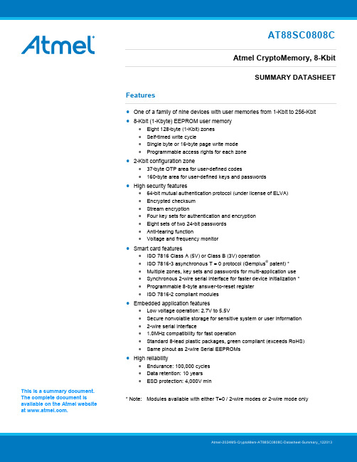
AT88SC0808CAtmel CryptoMemory, 8-KbitSUMMARY DATASHEETFeatures • One of a family of nine devices with user memories from 1-Kbit to 256-Kbit •8-Kbit (1-Kbyte) EEPROM user memory• Eight 128-byte (1-Kbit) zones • Self-timed write cycle• Single byte or 16-byte page write mode • Programmable access rights for each zone• 2-Kbit configuration zone• 37-byte OTP area for user-defined codes• 160-byte area for user-defined keys and passwords •High security features• 64-bit mutual authentication protocol (under license of ELVA) • Encrypted checksum • Stream encryption• Four key sets for authentication and encryption • Eight sets of two 24-bit passwords • Anti-tearing function• Voltage and frequency monitor•Smart card features• ISO 7816 Class A (5V) or Class B (3V) operation• ISO 7816-3 asynchronous T = 0 protocol (Gemplus ®patent) * • Multiple zones, key sets and passwords for multi-application use • Synchronous 2-wire serial interface for faster device initialization * • Programmable 8-byte answer-to-reset register •ISO 7816-2 compliant modules•Embedded application features• Low voltage operation: 2.7V to 5.5V• Secure nonvolatile storage for sensitive system or user information • 2-wire serial interface• 1.0MHz compatibility for fast operation• Standard 8-lead plastic packages, green compliant (exceeds RoHS) •Same pinout as 2-wire Serial EEPROMs•High reliability• Endurance: 100,000 cycles • Data retention: 10 years • ESD protection: 4,000V min* Note: Modules available with either T=0 / 2-wire modes or 2-wire mode onlyThis is a summary document. The complete document is available on the Atmel website at .AT88SC0808C [SUMMARY DATASHEET]Atmel-2024MS-CryptoMem-AT88SC0808C-Datasheet-Summary_1220132Table 1. Pin AssignmentFigure 1.Pin Configuration1. DescriptionThe Atmel ®AT88SC0808C member of the Atmel CryptoMemory ®family is a high-performance secure memory providing 8-Kbits of user memory with advanced security and cryptographic features built in. The user memory is divided into eight 128-byte zones, each of which may be individually set with different security access rights or effectively combined together to provide space for one to eight data files.1.1 Smart Card ApplicationsThe AT88SC0808C provides high security, low cost, and ease of implementation without the need for a microprocessor operating system. The embedded cryptographic engine provides for dynamic and symmetric mutual authentication between the device and host, as well as performing stream encryption for all data and passwords exchanged between the device and host. Up to four unique key sets may be used for these operations. The AT88SC0808C offers the ability to communicate with virtually any smart card reader using the asynchronous T = 0 protocol (Gemplus Patent) defined in ISO 7816-3.1.2 Embedded ApplicationsThrough dynamic and symmetric mutual authentication, data encryption, and the use of encrypted checksums, theAT88SC0808C provides a secure place for storage of sensitive information within a system. With its tamper detection circuits, this information remains safe even under attack. A 2-wire serial interface running at 1.0MHz is used for fast and efficientcommunications with up to 15 devices that may be individually addressed. The AT88SC0808C is available in industry standard 8-lead packages with the same familiar pinout as 2-wire Serial EEPROMs.V CC =C1RST=C2SCL/CLK=C3NC=C4ISO Smart Card ModuleC5=GND C6=NC C7=SDA/IO C8=NCNC NC NC GND123487658-lead SOIC, PDIP V CC NC SCL SDAV CC =C1NC=C2SCL/CLK=C3NC=C4TWI Smart Card ModuleC5=GND C6=NC C7=SDA/IO C8=NCAT88SC0808C [SUMMARY DATASHEET]Atmel-2024MS-CryptoMem-AT88SC0808C-Datasheet-Summary_1220133Figure 1-1. Block Diagram2.Pin Descriptions2.1Supply Voltage (V CC )The V CC input is a 2.7V to 5.5V positive voltage supplied by the host.2.2 Clock (SCL/CLK)In the asynchronous T = 0 protocol, the SCL/CLK input is used to provide the device with a carrier frequency f . The nominal length of one bit emitted on I/O is defined as an “elementary time unit” (ETU) and is equal to 372/f. When the synchronous protocol is used, the SCL/CLK input is used to positive edge clock data into the device and negative edge clock data out of the device.2.3 Reset (RST)The AT88SC0808C provides an ISO 7816-3 compliant asynchronous answer to reset sequence. When the reset sequence is activated, the device will output the data programmed into the 64-bit answer-to-reset register. An internal pull-up on the RST input pad allows the device to be used in synchronous mode without bonding RST. The AT88SC0808C does not support the synchronous answer-to-reset sequence2.4 Serial Data (SDA/IO)The SDA pin is bidirectional for serial data transfer. This pin is open-drain driven and may be wired with any number of other open drain or open collector devices. An external pull-up resistor should be connected between SDA and V CC . The value of this resistor and the system capacitance loading the SDA bus will determine the rise time of SDA. This rise time will determine the maximum frequency during read operations. Low value pull-up resistors will allow higher frequency operations while drawing higher average power. SDA/IO information applies to both asynchronous and synchronous protocols.When the synchronous protocol is used, the SCL/CLK input is used to positive edge clock data into the device and negative edge clock data out of the device.V CCAT88SC0808C [SUMMARY DATASHEET]Atmel-2024MS-CryptoMem-AT88SC0808C-Datasheet-Summary_12201343.*NOTICE: Stresses beyond those listed under “AbsoluteMaximum Ratings” may cause permanent damage to the device. This is a stress rating only and functional operation of the device at these or any other condition beyond those indicated in the operational sections of this specification is not implied. Exposure to absolute maximum rating conditions for extended periods of time may affect device reliability.Table 3-1.DC CharacteristicsNote:1. V IL min and V IH max are reference only and are not tested2. To prevent latch up conditions from occurring during power up of the AT88SCxxxxC, V CC must be turned onbefore applying V IH . For powering down, V IH must be removed before turning V CC offAT88SC0808C [SUMMARY DATASHEET]Atmel-2024MS-CryptoMem-AT88SC0808C-Datasheet-Summary_1220135Table 3-2.AC CharacteristicsApplicable over recommended operating range from V CC = +2.7 to 5.5V,4. Device Operation for Synchronous ProtocolsClock and Data Transitions:The SDA pin is normally pulled high with an external device. Data on the SDA pin may change only during SCL low time periods (see Figure 4-3 on page 7). Data changes during SCL high periods will indicate a start or stop condition as defined below.Start Condition:A high-to-low transition of SDA with SCL high is a start condition which must precede any other command (see Figure 4-4 on page 7).Stop Condition:A low-to-high transition of SDA with SCL high is a stop condition. After a read sequence, the stop command will place the EEPROM in a standby power mode (see Figure 4-4 on page 7).Acknowledge:All addresses and data words are serially transmitted to and from the EEPROM in 8-bit words. The EEPROM sends a zero to acknowledge that it has received each word. This happens during the ninth clock cycle (see Figure 4-5 on page 7). Memory Reset:After an interruption in protocol, power loss or system reset, any 2-wire part can be reset by following these steps: 1. Clock up to nine cycles2. Look for SDA high in each cycle while SCL is high3. Create a start conditionAT88SC0808C [SUMMARY DATASHEET] Atmel-2024MS-CryptoMem-AT88SC0808C-Datasheet-Summary_1220136 Figure 4-1. Bus Timing for 2-wire Communications:SCL: Serial Clock, SDA – Serial Data I/OFigure 4-2. Write Cycle Timing:SCL: Serial Clock, SDA – Serial Data I/ONote: The write cycle time t WR is the time from a valid stop condition of a write sequence to the end of the internalclear/write cycleSCLSDA INSDA OUTSTOPCONDITIONSTARTCONDITIONSCLSDAAT88SC0808C [SUMMARY DATASHEET]Atmel-2024MS-CryptoMem-AT88SC0808C-Datasheet-Summary_1220137Figure 4-3. Data ValidityFigure 4-4. Start and Stop DefinitionsFigure 4-5. Output AcknowledgeDATA CHANGE ALLOWEDDATA STABLEDATA STABLESDASCLSDASCLSTART STOPSCLDAT A INDAT A OUTEG D E L W O N K C A T R A T S 981AT88SC0808C [SUMMARY DATASHEET]Atmel-2024MS-CryptoMem-AT88SC0808C-Datasheet-Summary_12201385.Device Architecture5.1User ZonesThe EEPROM user memory is divided into eight zones of 1024 bits each. Multiple zones allow for different types of data or files to be stored in different zones. Access to the user zones is allowed only after security requirements have been met. These security requirements are defined by the user during the personalization of the device in the configuration memory. If the same security requirements are selected for multiple zones, then these zones may effectively be accessed as one larger zone.6. Control LogicAccess to the user zones occurs only through the control logic built into the device. This logic is configurable through access registers, key registers and keys programmed into the configuration memory during device personalization. Also implemented in the control logic is a cryptographic engine for performing the various higher-level security functions of the device.AT88SC0808C [SUMMARY DATASHEET]Atmel-2024MS-CryptoMem-AT88SC0808C-Datasheet-Summary_12201397. Configuration MemoryThe configuration memory consists of 2048 bits of EEPROM memory used for storing passwords, keys and codes and defining security levels to be used for each user zone. Access rights to the configuration memory are defined in the control logic and may not be altered by the user.AT88SC0808C [SUMMARY DATASHEET]Atmel-2024MS-CryptoMem-AT88SC0808C-Datasheet-Summary_122013108. Security FusesThere are three fuses on the device that must be blown during the device personalization process. Each fuse locks certain portions of the configuration memory as OTP memory. Fuses are designed for the module manufacturer, card manufacturer and card issuer and should be blown in sequence, although all programming of the device and blowing of the fuses may be performed at one final step.9. Protocol selectionThe AT88SC0808C supports two different communication protocols.• Smart Card Applications:The asynchronous T = 0 protocol defined by ISO 7816-3 is used for compatibility with the industry’s standard smart card readers• Embedded Applications:A 2-wire serial interface is used for fast and efficient communication with logic or controllersThe power-up sequence determines which of the two communication protocols will be used.9.1 Asynchronous T = 0 ProtocolThis power-up sequence complies with ISO 7816-3 for a cold reset in smart card applications.• V CC goes high; RST, I/O-SDA and CLK-SCL are low • Set I/O-SDA in receive mode • Provide a clock signal to CLK-SCL •RST goes high after 400 clock cyclesThe device will respond with a 64-bit ATR code, including historical bytes to indicate the memory density within theCryptoMemory family. Once the asynchronous mode has been selected, it is not possible to switch to the synchronous mode without powering off the device.Figure 9-1. Asynchronous T = 0 Protocol (Gemplus Patent)V cc I/O-SDARSTCLK-SCL9.2 Synchronous 2-wire Serial InterfaceThe synchronous mode is the default after powering up V CC due to an internal pull-up on RST. For embedded applications using CryptoMemory in standard plastic packages, this is the only communication protocol.• Power-up V CC , RST goes high also• After stable V CC , CLK-SCL and I/O-SDA may be drivenFigure 9-2. Synchronous 2-wire ProtocolNote:Five clock pulses must be sent before the first command is issued10. Communication Security ModesCommunications between the device and host operate in three basic modes. Standard mode is the default mode for the device after power-up. Authentication mode is activated by a successful authentication sequence. Encryption mode is activated by a successful encryption activation following a successful authentication. Table 10-1. Communication Security Modes (1)Note:1. Configuration data include viewable areas of the configuration zone except the passwords:• MDC: Modification Detection Code •MAC: Message Authentication CodeV cc I/O-SDARST CLK-SCL1234511. Security Options11.1 Anti-tearingIn the event of a power loss during a write cycle, the integrity of the device’s stored data may be recovered. This function is optional: the host may choose to activate the anti-tearing function, depending on application requirements. When anti-tearing is active, write commands take longer to execute, since more write cycles are required to complete them, and data are limited to eight bytes.Data are written first to a buffer zone in EEPROM instead of the intended destination address, but with the same accessconditions. The data are then written in the required location. If this second write cycle is interrupted due to a power loss, the device will automatically recover the data from the system buffer zone at the next power-up.In 2-wire mode, the host is required to perform ACK polling for up to 8mS after write commands when anti-tearing is active. At power-up, the host is required to perform ACK polling, in some cases for up to 2mS, in the event that the device needs to carry out the data recovery process.11.2 Write LockIf a user zone is configured in the write lock mode, the lowest address byte of an 8-byte page constitutes a write access byte for the bytes of that page.Example: The write lock byte at $080 controls the bytes from $080 to $087The write lock byte may also be locked by writing its least significant (rightmost) bit to “0”. Moreover, when write lock mode is activated, the write lock byte can only be programmed — that is, bits written to “0” cannot return to “1”.In the write lock configuration, only one byte can be written at a time. Even if several bytes are received, only the first byte will be taken into account by the device.12. Password VerificationPasswords may be used to protect read and/or write access of any user zone. When a valid password is presented, it ismemorized and active until power is turned off, unless a new password is presented or RST becomes active. There are eight password sets that may be used to protect any user zone. Only one password is active at a time, but write passwords give read access also..12.1 Authentication ProtocolThe access to a user zone may be protected by an authentication protocol. Any one of four keys may be selected to use with a user zone.The authentication success is memorized and active as long as the chip is powered, unless a new authentication is initialized or RST becomes active. If the new authentication request is not validated, the card loses its previous authentication and itshould be presented again. Only the last request is memorized.Note: Password and authentication may be presented at any time and in any order. If the trials limit has been reached (after four consecutive incorrect attempts), the password verification or authentication process will not be takeninto accountFigure 12-1. Password and Authentication OperationsREAD ACCESS12.2 ChecksumThe AT88SC0808C implements a data validity check function in the form of a checksum, which may function in standard,authentication or encryption modes.In the standard mode, the checksum is implemented as a Modification Detection Code (MDC), in which the host may read an MDC from the device in order to verify that the data sent was received correctly.In the authentication and encryption modes, the checksum becomes more powerful since it provides a bidirectional dataintegrity check and data origin authentication capability in the form of a Message Authentication Code (MAC). Only thehost/device that carried out a valid authentication is capable of computing a valid MAC. While operating in the authentication or encryption modes, the use of a MAC is required. For an ingoing command, if the device calculates a MAC different from the MAC transmitted by the host, not only is the command abandoned but the mode is also reset. A new authentication and/or encryption activation will be required to reactivate the MAC.12.3 EncryptionThe data exchanged between the device and the host during read, write and verify password commands may be encrypted to ensure data confidentiality.The issuer may choose to require encryption for a user zone by settings made in the configuration memory. Any one of four keys may be selected for use with a user zone. In this case, activation of the encryption mode is required in order to read/write data in the zone and only encrypted data will be transmitted. Even if not required, the host may elect to activate encryption provided the proper keys are known.12.4 Supervisor ModeEnabling this feature allows the holder of one specific password to gain full access to all eight password sets, including the ability to change passwords.12.5 Modify ForbiddenNo write access is allowed in a user zone protected with this feature at any time. The user zone must be written during device personalization prior to blowing the security fuses.12.6 Program OnlyFor a user zone protected by this feature, data within the zone may be changed from a “1” to a “0”, but never from a “0” to a “1”.13. Initial Device ProgrammingTo enable the security features of CryptoMemory, the device must first be personalized to set up several registers and load in the appropriate passwords and keys. This is accomplished through programming the configuration memory of CryptoMemory using simple write and read commands. To gain access to the configuration memory, the secure code must first besuccessfully presented. For the AT88SC0808C device, the secure code is $22 E8 3F. After writing and verifying data in the configuration memory, the security fuses must be blown to lock this information in the device. For additional information on personalizing CryptoMemory, please see the application notes Programming CryptoMemory for Embedded Applications and Initializing CryptoMemory for Smart Card Applications (at ).14.Note: 1. Formal drawings may be obtained from an Atmel sales office2. Both the J and P module packages are used for either ISO (T=0 / 2-wire mode) or TWI (2-wire mode only)15. Packaging InformationOrdering Code: MJ or MJTG Ordering Code: MP or MPTGModule Size: M2Dimension*: 12.6 x 11.4 [mm] Glob Top: Round - ∅ 8.5 [mm] Thickness: 0.58 [mm]Pitch: 14.25mm Module Size: M2Dimension*: 12.6 x 11.4 [mm]Glob Top: Square - 8.8 x 8.8 [mm] Thickness: 0.58 [mm]Pitch: 14.25mmNote: *The module dimensions listed refer to the dimensions of the exposed metal contact area. The actual dimensions of the module after excise or punching from the carrier tape are generally 0.4mm greater in both directions (i.e., apunched M2 module will yield 13.0 x 11.8mm)15.1 Atmel AT88SC0808C Package Marking Information15.2 Ordering Code: SH8S1 – 8-lead JEDEC SOIC15.3 Ordering Code: PU8P3 – 8-lead PDIP16. Revision History。
常见的单片机品牌与型号介绍

常见的单片机品牌与型号介绍单片机(Microcontroller Unit,简称MCU)作为嵌入式系统的核心部件,广泛应用于各种电子设备中。
随着科技的不断发展,市场上涌现了众多单片机品牌和型号。
本文将为大家介绍常见的单片机品牌与型号,供读者参考选择。
一、Atmel(爱特梅尔)Atmel是全球领先的单片机厂商之一,其产品在市场上占据了显著的份额。
Atmel的单片机以高性能、低功耗、易用性和可靠性著称。
以下是Atmel单片机的几个典型型号:1. ATmega328P:这是一款广泛应用于Arduino开发板中的单片机,具有32KB的Flash存储器和2KB的SRAM,适合中小规模的嵌入式应用。
2. ATtiny85:这是一款微型单片机,具有8KB的Flash存储器和512字节的SRAM,尺寸小巧,适合于资源受限的应用场景。
3. ATSAM4S16C:这是一款高性能的ARM Cortex-M4核心单片机,具有256KB的Flash存储器和64KB的SRAM,适用于复杂的嵌入式系统设计。
二、STMicroelectronics(意法半导体)STMicroelectronics是全球领先的半导体解决方案供应商之一,其STMicroelectronics单片机也备受认可。
STMicroelectronics的单片机以性能稳定、丰富的外设接口以及低功耗特性而著称。
以下是几款常见的型号:1. STM32F103C8T6:这是STMicroelectronics的一款32位ARM Cortex-M3核心单片机,具有64KB的Flash存储器和20KB的SRAM,适合于中等规模的嵌入式应用。
2. STM8S003F3P6:这是STMicroelectronics的一款8位单片机,具有8KB的Flash存储器和1KB的SRAM,适合于资源受限的应用场景。
3. STM32F407VET6:这是STMicroelectronics的一款高性能32位ARM Cortex-M4核心单片机,具有512KB的Flash存储器和192KB的SRAM,适用于要求较高计算能力的嵌入式系统设计。
Atmel ATmegaS128 微控制器商品说明书

The new Atmel ® AVR ® ATmegaS128 microcontroller (MCU) brings the industry-leading AVR core to the aerospace industry. The ATmegaS128 MCU is designed for enhanced radiation performance and increased reliability in space applications. It takes advantage of mature Atmel AVR tools designed and used in the mass market worldwide for many years. The ATmegaS128 microcontroller targets many of the most common space applications, which typically require a small footprint, low power and analog control of motors and sensors.Key FeaturesHigh-performance, Low-power 8-bit Atmel AVR MCU• Advanced RISC architecture / Up to 8MIPS• On-chip 2-cycle multiplier• 3V-3.6V / 0 - 8MHz operating voltages & speed grades High-endurance Non-volatile Memory • 128 Kbytes of Flash program memory• 4 Kbytes EEPROM – 4 Kbytes internal SRAM1Advance Risc Architecture 8 Mips3.0 3-55 • Up to 64 Kbytes optionalexternal memory space • SPI interface for in-system programmingPeripheral Features • Two 8-bit and two 16-bit timers/counters • 6 PWM channels • 8-channel, 10-bit ADC• TWI/USARTs/SPI serial interface • Programmable watchdog timer • On-chip analog comparator Special Microcontroller Features• Power-on reset and programmable brown-out detection• Internal calibrated RC oscillator • External and internal interrupt sources• Six Sleep modes: Idle, ADC Noise Reduction, Power-save, Power-down, Standby, and Extended StandbyKey Highlights for Space Environment• Full wafer lot traceability • 64-lead ceramic package (CQFP) • Space screening • Space qualification• Total ionizing Dose: up to 30 Krad (Si)• Single event latch-up LET > 62.5MeV.cm²/mg• Single event upset LET > 3 MeV.cm²/mg•SEU 10-3 to 10-1 error/ device/dayATmegaS128 Starter kitTo ease your design process and reduce time-to-market, Atmel delivers a complete starter kit STK600 and development system for the ATmegaS128 AVR microcontroller. With its advanced features for proto-typing and testing new designs, the kit gives designers a head start for developing code on AVR devices. Customers can start with the industrial version using the ATmega128 MCU or the Space Version ATme-gaS128 device as both share the same pinout.Atmel Corporation 1600 Technology Drive, San Jose, CA 95110 USA T : (+1)(408) 441. 0311 F : (+1)(408) 436. 4200 | © 2015 Atmel Corporation. / Rev.: Atmel-45160A-ATmegaS128-Aerospace-Rad-Tolerant-Flyer_E_US_102015Atmel,® Atmel logo and combinations thereof, Enabling Unlimited Possibilities,® and others are registered trademarks or trademarks of Atmel Corporation in U. S. and other countries. Other terms and product names may be trademarks of others.Disclaimer: The information in this document is provided in connection with Atmel products. No license, express or implied, by estoppel or otherwise, to any intellectual property right is granted by this document or in connection with the sale of Atmel products. EXCEPT AS SET FORTH IN THE ATMEL TERMS AND CONDITIONS OF SALES LOCATED ON THE ATMEL WEBSITE, ATMEL ASSUMES NO LIABILITY WHATSOEVER AND DISCLAIMS ANY EXPRESS, IMPLIED OR STATUTORY WARRANTY RE-LATING TO ITS PRODUCTS INCLUDING, BUT NOT LIMITED TO, THE IMPLIED WARRANTY OF MERCHANTABILITY, FITNESS FOR A PARTICULAR PURPOSE, OR NON-INFRINGEMENT. IN NO EVENT SHALL ATMEL BE LIABLE FOR ANY DIRECT, INDIRECT, CONSEQUENTIAL, PUNITIVE, SPECIAL OR INCIDENTAL DAMAGES (INCLUDING, WITHOUT LIMITATION, DAMAGES FOR LOSS AND PROFITS, BUSINESS INTERRUPTION, OR LOSS OF INFORMATION) ARISING OUT OF THE USE OR INABILITY TO USE THIS DOCUMENT, EVEN IF ATMEL HAS BEEN ADVISED OF THE POSSIBILITY OF SUCH DAMAGES. Atmel makes no representations or warranties with respect to the accuracy or completeness of the contents of this document and reserves the right to make changes to specifications and products descriptions at any time without notice. Atmel does not make any commitment to update the information contained herein. Unless specifically provided otherwise, Atmel products are not suitable for, and shall not be used in, automotive applications. Atmel products are not intended, authorized, or warranted for use as components in applications intended to support or sustain life.Atmel StudioAtmel Studio is the integrated development platform (IDP) for developing and debugging Atmel AVR and Atmel | SMART ARM ® processor-based MCU applications. The Atmel Studio IDP gives you a seamless and easy-to-use environment to write, build and debug your applications written in C/C++ or assembly code. Atmel Studio supports all 8- and 32-bit AVR MCUs. It also connects seamlessly to Atmel debuggers and development kits.Atmel Software FrameworkThe Atmel Software Framework (ASF) is an MCU software library providing a 1,600 project examples of embedded software for Atmel Flash-based MCUs, including AVR and Atmel | SMART devices. This library contains basic C code examples for all ATmegaS128 peripherals.Application NotesIn addition to the Atmel Software framework, Atmel provides a broad range of application notes to implement different peripherals of the ATmegaS128 device. Most of those ap-plication notes are provided with source code in C language.。
常用的单片机品牌和型号介绍

常用的单片机品牌和型号介绍单片机(Microcontroller)是一种集成了微处理器核心、存储器和各种外设接口的集成电路,广泛应用于嵌入式系统中。
单片机能够完成各种控制和计算任务,因此在电子领域中使用非常广泛。
本文将介绍几个常用的单片机品牌和型号,以帮助读者选择适合自己项目的单片机。
一、STMicroelectronicsSTMicroelectronics(意法半导体)是全球领先的半导体供应商之一,提供多种单片机产品。
其中,STM32系列是STMicroelectronics最为著名的单片机系列之一,基于ARM Cortex-M内核。
STM32系列广泛应用于各种嵌入式设备,具有高性能、低功耗等特点。
常见的型号包括STM32F0、STM32F1、STM32F4等,适用于不同的应用场景。
二、AtmelAtmel是一家美国公司,也是全球最大的单片机供应商之一。
Atmel的AVR系列单片机以其高性能和易用性而闻名。
AVR系列单片机具有低功耗、快速执行速度和丰富的外设接口,非常适合于各种嵌入式应用。
其中,ATmega328P是最常用的型号之一,广泛使用于Arduino开发板等项目中。
三、Texas InstrumentsTexas Instruments(德州仪器)是一家世界领先的半导体公司,提供多种单片机产品。
MSP430系列是Texas Instruments的一系列低功耗、高集成度的单片机产品,适用于各种便携式设备和电池供电系统。
MSP430系列单片机具有强大的外设功能和丰富的存储器选项,常见的型号有MSP430G2553、MSP430F5529等。
四、MicrochipMicrochip是一家专注于微控制器和模拟半导体的供应商,其PIC 单片机系列非常知名。
PIC系列单片机具有低功耗、高稳定性和广泛的外设接口,适用于各种应用场景。
其中,PIC16F877A是最常用的型号之一,常见于工业自动化、家电控制等领域。
部分51单片机系列品牌和型号整理

部分51单片机系列品牌和型号整理51单片机作为一种常用的微控制器,有着广泛的应用领域。
本文将对一些常见的51单片机品牌和型号进行整理,以帮助读者更好地选择适合自己需求的产品。
1. STC系列STC系列是由中国的宏晶科技生产的一类51单片机。
宏晶科技在国内有着较高的知名度,并且产品质量良好。
STC系列单片机有着丰富的型号选择,从较低性能的51系列到高性能的ARM Cortex-M0系列都有覆盖。
其中较为常见的型号有STC89C52、STC12C5A60S2、STC15W408AS等,它们在不同领域都有着广泛的应用。
2. NXP系列NXP公司是一家全球知名的半导体制造商,在51单片机市场上也有着一席之地。
NXP系列的单片机性能稳定可靠,并且具有较高的集成度。
常见的型号有P89V51RD2、P89V51RB2、P89V660等,它们在汽车电子、工控领域等有着广泛的应用。
3. TI系列德州仪器(TI)公司也是一家全球知名的半导体制造商,其51单片机产品具有优良的性能和稳定性。
TI系列的单片机在银行、电源管理等领域有着广泛的应用。
常见的型号有TMS320F28335、TMS320F28027等,它们具有较高的运算速度和丰富的外设接口。
4. Atmel系列Atmel公司是一家专业从事微控制器、存储器和半导体解决方案的制造商,其51单片机产品在市场上有着良好的声誉。
Atmel系列单片机以其低功耗和可靠性而受到广泛认可。
常见的型号有AT89C51、AT89S52等,它们在消费电子、智能家居等领域应用广泛。
5. Silicon Labs系列Silicon Labs是一家总部位于美国的半导体公司,其51单片机产品拥有较高的性能和集成度。
Silicon Labs系列的单片机在无线通信、工控领域等有着广泛的应用。
常见的型号有C8051F120、C8051F340等,它们具有较高的运算速度和丰富的外设接口。
6. Renesas系列Renesas电子公司是一家日本半导体制造商,其51单片机产品具有较高的可靠性和稳定性。
Atmel 2322I 可编程串行存储器数据手册说明书
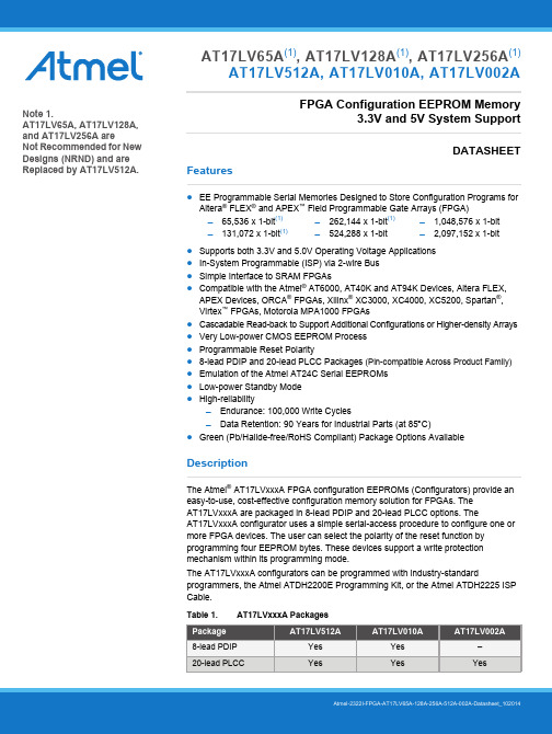
Features●EE Programmable Serial Memories Designed to Store Configuration Programs forAltera ® FLEX ® and APEX ™ Field Programmable Gate Arrays (FPGA)●Supports both 3.3V and 5.0V Operating Voltage Applications ●In-System Programmable (ISP) via 2-wire Bus ●Simple Interface to SRAM FPGAs●Compatible with the Atmel ® AT6000, AT40K and AT94K Devices, Altera FLEX,APEX Devices, ORCA ® FPGAs, Xilinx ® XC3000, XC4000, XC5200, Spartan ®, Virtex ™ FPGAs, Motorola MPA1000 FPGAs●Cascadable Read-back to Support Additional Configurations or Higher-density Arrays ●Very Low-power CMOS EEPROM Process ●Programmable Reset Polarity●8-lead PDIP and 20-lead PLCC Packages (Pin-compatible Across Product Family)●Emulation of the Atmel AT24C Serial EEPROMs ●Low-power Standby Mode ●High-reliabilityEndurance: 100,000 Write CyclesData Retention: 90 Years for Industrial Parts (at 85 C)●Green (Pb/Halide-free/RoHS Compliant) Package Options AvailableDescriptionThe Atmel ® AT17LVxxxA FPGA configuration EEPROMs (Configurators) provide an easy-to-use, cost-effective configuration memory solution for FPGAs. The AT17LVxxxA are packaged in 8-lead PDIP and 20-lead PLCC options. TheAT17LVxxxA configurator uses a simple serial-access procedure to configure one or more FPGA devices. The user can select the polarity of the reset function by programming four EEPROM bytes. These devices support a write protection mechanism within its programming mode.The AT17LVxxxA configurators can be programmed with industry-standardprogrammers, the Atmel ATDH2200E Programming Kit, or the Atmel ATDH2225 ISP Cable.Table 1.AT17LVxxxA Packages65,536 x 1-bit (1)131,072 x 1-bit (1)262,144 x 1-bit (1)524,288 x 1-bit 1,048,576 x 1-bit 2,097,152 x 1-bitAT17LV65A (1), AT17LV128A (1), AT17LV256A (1)AT17LV512A, AT17LV010A, AT17LV002AFPGA Configuration EEPROM Memory3.3V and 5V System SupportDATASHEETNote 1.AT17LV65A, AT17LV128A, and AT17LV256A areNot Recommended for New Designs (NRND) and are Replaced by AT17LV512A.AT17LV65A/128A/256A/512A/002A [DATASHEET]Atmel-2322I-FPGA-AT17LV65A-128A-256A-512A-002A-Datasheet_10201421.Pin Configuration and DescriptionsTable 1-1.Pin Descriptions3AT17LV65A/128A/256A/512A/002A [DATASHEET]Atmel-2322I-FPGA-AT17LV65A-128A-256A-512A-002A-Datasheet_102014Table 1-2.Pin ConfigurationsNotes:1.The nCASC feature is not available on the AT17LV65A (NRND) device.2.The AT17LV65A, AT17LV128A, and AT17LV256A are not recommended for new designs.Figure 1-1.Pinouts (1)Notes: 1. Drawings are not to scale.2. This pin is only available on the AT17LV65A/128A/256A (NRND).3. This pin is only available on the AT17LV512A/010A/002A.4. The nCASC feature is not available on the AT17LV65A (NRND).8-lead PDIP(Top View)DATA DCLK(WP (2)) RESET/OEnCSV CC SER_EN nCASC (4) (A2)GND1234876520-lead PLCC(Top View)N CD A T AN CV C CN CSER_EN NC NCNC (READY (3))NCDCLK WP1(3)NC NC(WP (2)) RESET/OEn C SG N DN C(A 2) n C A S C (4)N C3212019910111213456781817161514AT17LV65A/128A/256A/512A/002A [DATASHEET]Atmel-2322I-FPGA-AT17LV65A-128A-256A-512A-002A-Datasheet_10201442.Block DiagramFigure 2-1.Block DiagramNotes:1.This pin is only available on AT17LV65A/128A/256A (NRND).2.This pin is only available on AT17LV512A/010A/002A.3.The nCASC feature is not available on the AT17LV65A (NRND).(WP (1))5AT17LV65A/128A/256A/512A/002A [DATASHEET]Atmel-2322I-FPGA-AT17LV65A-128A-256A-512A-002A-Datasheet_1020143.Device DescriptionThe control signals for the configuration EEPROM (nCS, RESET/OE and DCLK) interface directly with the FPGA device control signals. All FPGA devices can control the entire configuration process and retrieve data from the configuration EEPROM without requiring an external controller.The configuration EEPROM’s RESET/OE and nCS pins control the tri-state buffer on the DATA output pin and enable the address counter and the oscillator. When RESET/OE is driven Low, the configuration EEPROM resets its address counter and tri-states its DATA pin. The nCS pin also controls the output of the AT17LVxxxA configurator. If nCS is held High after the RESET/OE pulse, the counter is disabled and the DATA output pin is tri-stated. When nCS is driven subsequently Low, the counter and the DATA output pin are enabled. When RESET/OE is driven Low again, the address counter is reset and the DATA output pin is tri-stated, regardless of the state of the nCS.When the configurator has driven out all of its data and nCASC is driven Low, the device tri-states the DATA pin to avoid contention with other configurators. Upon power-up, the address counter is automatically reset.This is the default setting for the device. Since almost all FPGAs use RESET Low and OE High, this document will describe RESET/OE.4.FPGA Master Serial Mode SummaryThe I/O and logic functions of any SRAM-based FPGA are established by a configuration program. Theprogram is loaded either automatically upon power-up, or on command, depending on the state of the FPGA mode pins. In Master mode, the FPGA automatically loads the configuration program from an external memory. The AT17LVxxxA Serial Configuration EEPROM has been designed for compatibility with the Master Serial mode.This document discusses the Altera FLEX FPGA device interfaces.5.Control of ConfigurationMost connections between the FPGA device and the AT17LVxxxA Serial EEPROM are simple and self-explanatory.●The DATA output of the AT17LVxxxA configurator drives DIN of the FPGA devices.●The master FPGA DCLK output or external clock source drives the DCLK input of the AT17LVxxxA configurator.●The nCASC output of any AT17LVxxxA configurator drives the nCS input of the next configurator in a cascaded chain of EEPROMs.●SER_EN must be connected to V CC (except during ISP).AT17LV65A/128A/256A/512A/002A [DATASHEET]Atmel-2322I-FPGA-AT17LV65A-128A-256A-512A-002A-Datasheet_10201466.Cascading Serial Configuration EEPROMsFor multiple FPGAs configured as a daisy-chain, or for FPGAs requiring larger configuration memories, cascaded configurators provide additional memory.After the last bit from the first configurator is read, the next clock signal to the configurator asserts its nCASC output low and disables its DATA line driver. The second configurator recognizes the low level on its nCS input and enables its DATA output.After configuration is complete, the address counters of all cascaded configurators are reset if the RESET/OE on each configurator is driven to a Low level.If the address counters are not to be reset upon completion, then the RESET/OE input can be tied to a High level.The AT17LV65A (NRND) does not have the nCASC feature to perform cascaded configurations.7.AT17LVxxxA Reset PolarityThe AT17LVxxxA configurator allows the user to program the polarity of the RESET/OE pin as either RESET/OE or RESET/OE. This feature is supported by industry-standard programmer algorithms.8.Programming ModeThe programming mode is entered by bringing SER_EN Low. In this mode the chip can be programmed by the 2-wire serial bus. The programming is done at V CC supply only. Programming super voltages are generated inside the chip.9.Standby ModeThe AT17LVxxxA enters a low-power standby mode whenever nCS is asserted High. In this mode,the configurator consumes less than 150μA of current at 3.3V. The output remains in a high-impedance state regardless of the state of the RESET/OE input.7AT17LV65A/128A/256A/512A/002A [DATASHEET]Atmel-2322I-FPGA-AT17LV65A-128A-256A-512A-002A-Datasheet_10201410.Electrical Specifications10.1Absolute Maximum Ratings*10.2Operating ConditionsTable 10-1.Operating Conditions10.3DC CharacteristicsTable 10-2.DC Characteristics for V CC = 3.3V ± 10%Note:1.The AT17LV65A, AT17LV128A, and AT17LV256A are not recommended for new designs.Operating Temperature . . . . . . . . . . . .-40︒C to +85︒C Storage Temperature. . . . . . . . . . . . .-65︒C to +150︒C Voltage on Any Pinwith Respect to Ground . . . . . . . . .-0.1V to V CC +0.5V Supply Voltage (V CC ) . . . . . . . . . . . . . . -0.5V to +7.0V Maximum Soldering Temp. (10s @ 1/16 in.) . . .260︒C ESD (R ZAP = 1.5K, C ZAP = 100 pF)2000V*Notice:Stresses beyond those listed under AbsoluteMaximum Ratings may cause permanent damage to the device. This is a stress rating only and functional operation of the device at these or any other conditions beyond those listed underoperating conditions is not implied. Exposure to Absolute Maximum Rating conditions for extended periods of time may affect device reliability.AT17LV65A/128A/256A/512A/002A [DATASHEET]Atmel-2322I-FPGA-AT17LV65A-128A-256A-512A-002A-Datasheet_1020148Table 10-3.DC Characteristics for V CC = 5.0V ± 10%Note:1.The AT17LV65A, AT17LV128A, and AT17LV256A are not recommended for new designs.10.4AC CharacteristicsTable 10-4.AC Characteristics for V CC = 3.3V ± 10%Notes:1.AC test lead = 50pF.2.Float delays are measured with 5pF AC loads. Transition is measured ± 200mV from steady-state active levels.3.The AT17LV65A, AT17LV128A, and AT17LV256A are not recommended for new designs.9AT17LV65A/128A/256A/512A/002A [DATASHEET]Atmel-2322I-FPGA-AT17LV65A-128A-256A-512A-002A-Datasheet_102014Notes:1.AC test lead = 50pF.2.Float delays are measured with 5pF AC loads. Transition is measured ± 200mV from steady-state active levels.3.The AT17LV65A, AT17LV128A, and AT17LV256A are not recommended for new designs.Table 10-6.AC Characteristics for V CC = 5.0V ± 10%Notes:1.AC test lead = 50pF.2.Float delays are measured with 5pF AC loads. Transition is measured ± 200mV from steady-state active levels.3.The AT17LV65A, AT17LV128A, and AT17LV256A are not recommended for new designs.AT17LV65A/128A/256A/512A/002A [DATASHEET]Atmel-2322I-FPGA-AT17LV65A-128A-256A-512A-002A-Datasheet_10201410Notes:1.AC test lead = 50pF.2.Float delays are measured with 5pF AC loads. Transition is measured ± 200mV from steady-state active levels.3.The AT17LV65A, AT17LV128A, and AT17LV256A are not recommended for new designs.Figure 10-1.AC WaveformsFigure 10-2.AC Waveforms when CascadingnCSRESET/OEDCLKDATAnCSRESET/OEDCLKDATAnCASL11AT17LV65A/128A/256A/512A/002A [DATASHEET]Atmel-2322I-FPGA-AT17LV65A-128A-256A-512A-002A-Datasheet_10201410.5Thermal Resistance CoefficientsTable 10-8.Thermal Resistance CoefficientsNotes:1.Airflow = 0ft/min.2.The AT17LV65A, AT17LV128A, and AT17LV256A are not recommended for new designs.AT17LV65A/128A/256A/512A/002A [DATASHEET]Atmel-2322I-FPGA-AT17LV65A-128A-256A-512A-002A-Datasheet_1020141211.1Ordering Code Detail11.2Ordering InformationNotes:e 512-Kbit density parts to replace Altera EPC1441.e 1-Mbit density parts to replace Altera EPC1e 2-Mbit density parts to replace Altera EPC2.4.The AT17LVxxxA do not support JTAG programming. They use a 2-wire serial interface for in-system programming.A T 17L V 512A -10P UAtmel DesignatorProduct FamilyDevice DensitySpecial PinoutsProduct Variation65 = 65 kilobit 128 = 128 kilobit 256 = 256 kilobit 512 = 512 kilobit010 = 1 Mbit 002 = 2 MbitA = AlteraBlank = Xilinx/Atmel/Other17LV = FPGA EEPROM Configuration MemoryPackage Device GradeU = Green, Industrial Temperature Range (-40°C to +85°C)10 = Default ValuePackage OptionP = 8P3, 8-lead PDIP J =20J, 20-lead PLCC12.18P3 – PDIPAT17LV65A/128A/256A/512A/002A [DATASHEET]13Atmel-2322I-FPGA-AT17LV65A-128A-256A-512A-002A-Datasheet_102014AT17LV65A/128A/256A/512A/002A [DATASHEET]Atmel-2322I-FPGA-AT17LV65A-128A-256A-512A-002A-Datasheet_1020141412.220J – PLCC15AT17LV65A/128A/256A/512A/002A [DATASHEET]Atmel-2322I-FPGA-AT17LV65A-128A-256A-512A-002A-Datasheet_10201413.Revision HistoryX X X X X XAtmel Corporation1600 Technology Drive, San Jose, CA 95110 USAT: (+1)(408) 441.0311F: (+1)(408) 436.4200|© 2014 Atmel Corporation. / Rev.: Atmel-2322I-FPGA-AT17LV65A-128A-256A-512A-002A-Datasheet_102014.Atmel ®, Atmel logo and combinations thereof, Enabling Unlimited Possibilities ®, and others are registered trademarks or trademarks of Atmel Corporation in U.S. and other countries. Other terms and product names may be trademarks of others.DISCLAIMER: The information in this document is provided in connection with Atmel products. No license, express or implied, by estoppel or otherwise, to any intellectual property right is granted by this document or in connection with the sale of Atmel products. EXCEPT AS SET FORTH IN THE ATMEL TERMS AND CONDITIONS OF SALES LOCATED ON THE ATMEL WEBSITE, ATMEL ASSUMES NO LIABILITY WHATSOEVER AND DISCLAIMS ANY EXPRESS, IMPLIED OR STATUTORY WARRANTY RELATING TO ITS PRODUCTS INCLUDING, BUT NOT LIMITED TO, THE IMPLIED WARRANTY OF MERCHANTABILITY, FITNESS FOR A PARTICULAR PURPOSE, OR NON-INFRINGEMENT. IN NO EVENT SHALL ATMEL BE LIABLE FOR ANY DIRECT, INDIRECT, CONSEQUENTIAL, PUNITIVE, SPECIAL OR INCIDENTAL DAMAGES (INCLUDING, WITHOUT LIMITATION, DAMAGES FOR LOSS AND PROFITS, BUSINESS INTERRUPTION, OR LOSS OF INFORMATION) ARISING OUT OF THE USE OR INABILITY TO USE THIS DOCUMENT, EVEN IF ATMEL HAS BEEN ADVISED OF THE POSSIBILITY OF SUCH DAMAGES. Atmel makes no representations or warranties with respect to the accuracy or completeness of the contents of this document and reserves the right to make changes to specifications and products descriptions at any time without notice. Atmel does not make any commitment to update the information contained herein. Unless specifically provided otherwise, Atmel products are not suitable for, and shall not be used in, automotive applications. Atmel products are not intended,authorized, or warranted for use as components in applications intended to support or sustain life.SAFETY-CRITICAL, MILITARY, AND AUTOMOTIVE APPLICATIONS DISCLAIMER: Atmel products are not designed for and will not be used in connection with any applications where the failure of such products would reasonably be expected to result in significant personal injury or death (“Safety-Critical Applications”) without an Atmel officer's specific written consent. Safety-Critical Applications include, without limitation, life support devices and systems, equipment or systems for the operation of nuclear facilities and weapons systems.Atmel products are not designed nor intended for use in military or aerospace applications or environments unless specifically designated by Atmel as military-grade. Atmel products are not designed nor intended for use in automotive applications unless specifically designated by Atmel as automotive-grade.。
ATMEL命名规则

ATMEL命名规则
IC 封装及命名规则--- ATMEL ATMEL产品型号命名AT XX X XX XX X X X
1 2 3 4 5 6
1.前缀:ATMEL 公司产品代号
2.器件型号
3.速度
4.封装形式:
A TQFP 封装
B 陶瓷钎焊双列直插
C 陶瓷熔封
D 陶瓷双列直插
F 扁平封装
G 陶瓷双列直插,一次可编程
J 塑料J 形引线芯片载体
K 陶瓷J 形引线芯片载体
L 无引线芯片载体
M 陶瓷模块
N 无引线芯片载体,一次可编程
P 塑料双列直插
Q 塑料四面引线扁平封装
R 微型封装集成电路
S 微型封装集成电路
T 薄型微型封装集成电路
U 针阵列
V 自动焊接封装
W 芯片
Y 陶瓷熔封
Z 陶瓷多芯片模块
5.温度范围:
C 0℃至70℃,
I -40℃至85℃,
M -55℃至125℃
6.工艺:
空白标准
/883 Mil-Std-883, 完全符合B 级B Mil-Std-883,不符合B 级。
atmel简介

爱特梅尔半导体成立于1984年,总部位于美国。
是世界上高级半导体产品设计、制造和行销的领先者,产品包括了微处理器、可编程逻辑器件、非易失性存储器、安全芯片、混合信号及RF射频集成电路。
通过这些核心技术的组合,ATMEL生产出了各种通用目的及特定应用的系统级芯片,以满足当今电子系统设计工程师不断增长和演进的需求。
ATMEL在系统级集成方面所拥有的世界级专业知识和丰富的经验使其产品可以在现有模块的基础上进行开发,保证最小的开发延期和风险。
凭借业界最广泛的知识产权(IP)组合,Atmel提供电子系统完整的系统解决方案的厂商。
这使客户能够带领他们与市场的电子产品的体积更小,更聪明,更符合成本效益比以往任何时候都通用的服务。
Atmel集成电路的主要集中在消费,工业,安全,通信,计算和汽车市场。
Atmel公司的股票代码为“交易代码”在纳斯达克股票市场上市。
ATMEL公司是世界上高级半导体产品设计、制造和行销的领先者,产品包括了微处理器、可编程逻辑器件、非易失性存储器、安全芯片、混合信号及RF射频集成电路。
通过这些核心技术的组合,ATMEL生产出了各种通用目的及特定应用的系统级芯片,以满足当今电子系统设计工程师不断增长和演进的需求。
ATMEL在系统级集成方面所拥有的世界级专业知识和丰富的经验使其产品可以在现有模块的基础上进行开发,保证最小的开发延期和风险。
通过分布于超过60个国家的生产、工程、销售及分销网络,ATMEL承诺面向客户,为北美、欧洲和亚洲的电子市场服务。
确保及时介绍产品以及对客户持续的支持已经使ATMEL的产品成为最新电子产品的核心器件。
这些产品进而帮助最终用户完成更多的工作,享受更多的便利并保持与外界的沟通,不论身在何处。
ATMEL帮助客户设计更小、更便宜、更多特性的产品来领导市场。
因此,那些领导全球革新的公司都选择ATMEL的高性能产品来加快自身产品上市,并使自己的产品能够从竞争的产品之中区分出来,不论是传统的市场还是正在发展的市场。
Atmel

Atmel (艾特梅尔)
Atmel 公司成立于1984年,总部在美国加州,全球有超过5000名员
工。
高峰时期年销售额超过15亿美金,市值超过30亿美金。
其单片机
产品和EEPROM 产品应用很广泛,在汽车电子、射频、安全存储产品上
也有一定优势。
∙ ATmega 系列单片机
∙ ATtiny 系列单片机
∙ AVR32系列单片机
∙ ATxmega 系列单片机
∙ 8051单片机
∙ AT90系列单片机
∙ EEPROM 存储器
∙ 汽车电子单片机
∙ 触摸屏控制IC
∙ 其它单片机
∙ 其它存储器
∙ RF 收发器
Xilinx 公司成立于1984年,总部在美国加州,员工超过3000名,年销售额超过20亿美金,市值达70亿美金。
是全球可编程平台解决方案的领导者,其FPGA 产品被广泛应用于通讯、网络、工控、航天、军工等各个技术领域。
∙ Virtex-6 FPGA (XC6V)
∙ Virtex-5 FPGA (XC5V)
∙ Virtex-II FPGA (XC2V)
∙ Virtex-E FPGA (XCV5)
∙ SPARTAN-6 FPGA (XC6S)
∙ SPARTAN-3 FPGA (XC3S)
∙ CoolRunner-II CPLD (XC2C)
∙ 配置存储器
∙ 其它FPGA
∙ 其它CPLD。
ATMEGA16A中文资料
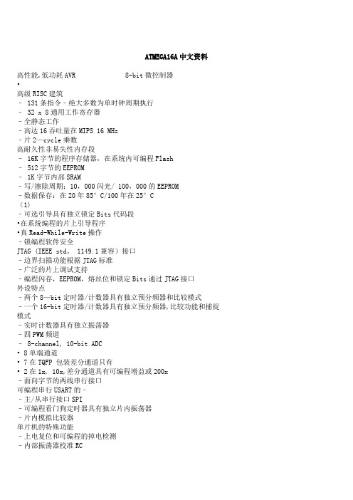
ATMEGA16A中文资料高性能,低功耗AVR 8-bit微控制器•高级RISC建筑– 131条指令–绝大多数为单时钟周期执行– 32 x 8通用工作寄存器–全静态工作–高达16吞吐量在MIPS 16 MHz–片2—cycle乘数高耐久性非易失性内存段– 16K字节的程序存储器,在系统内可编程Flash– 512字节的EEPROM– 1K字节内部SRAM–写/擦除周期:10,000闪光/ 100,000的EEPROM–数据保存:在20年85°C/100年在25°C(1)–可选引导具有独立锁定Bits代码段•在系统编程的片上引导程序•真Read-While-Write操作–锁编程软件安全JTAG (IEEE std。
1149.1兼容)接口–边界扫描功能根据JTAG标准–广泛的片上调试支持–编程闪存,EEPROM,熔丝位和锁定Bits通过JTAG接口外设特点–两个8—bit定时器/计数器具有独立预分频器和比较模式–一个16-bit定时器/计数器具有独立预分频器,比较功能和捕捉模式–实时计数器具有独立振荡器–四PWM频道– 8-channel, 10-bit ADC• 8单端通道• 7在TQFP 包装差分通道只有• 2在1x, 10x,差分通道具有可编程增益或200x–面向字节的两线串行接口可编程串行USART的––主/从串行接口SPI–可编程看门狗定时器具有独立片内振荡器–片内模拟比较器单片机的特殊功能–上电复位和可编程的掉电检测–内部振荡器校准RC–外部和内部中断源– 6种睡眠模式:空闲,ADC降噪,省电,省电,待机和扩展待机I / O和封装– 32可编程I / O线– 40—pin PDIP, 44—lead TQFP,和44—pad QFN/MLF 工作电压– 2。
7为- 5。
5V ATmega16A速度等级– 0 —为16 MHz ATmega16A功耗@ 1 MHz, 3V,和25°C为ATmega16A–活动:0。
Atmel Corporation (ATMEL,爱特美尔)

Atmel Corporation (ATMEL,爱特美尔)
爱特美尔公司1984年成立,专业设计、生产、销售一系列高性能半导体器件,包括逻辑器件、非易失存储器、混合信号IC和射频IC。
也是为数不多的能够在一个芯片上集成高密度存储、逻辑和模拟功能的厂家之一。
公司采用最先进的晶片工艺制造芯片,包括BiCMOS、CMOS和新兴的SiGe技术。
爱特美尔公司总部设在美国加州圣约瑟市,在美国、欧洲有多家制造工厂,其中包括设在法国的世界一流的8英寸、0.25微米晶片制造厂。
公司在全球设立了多个办事处。
此外,公司的产品还通过遍布全球的授权销售代表和分销商销往世界各地。
主营产品:
专业设计、生产、销售一系列高性能半导体器件,包括逻辑器件、非易失存储器、混合信号IC和射频IC。
也是为数不多的能够在一个芯片上集成高密度存储、逻辑和模拟功能的厂家之一。
厂商官网:
/
相关型号:
ATMEGA8L-8AUAT89C2051-24PUATMEGA128-16AUATMEGA48V-10AUATMEGA128L-8AU ATMEGA16L-8AUATMEGA32L-8AUATMEGA8-16AUATMEGA64-16AUAT24C02
型号索引:
102030405060708090100110120130140150更多。
单片机种类介绍
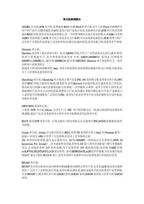
单片机种类简介ATMEL公司的AVR单片机,是增强型RISC内载Flash的单片机,芯片上的Flash存储器附在用户的产品中,可随时编程,再编程,使用户的产品设计容易,更新换代方便.A VR单片机采用增强的RISC结构,使其具有高速处理能力,在一个时钟周期内可执行复杂的指令,每MHz可实现1MIPS的处理能力.A VR单片机工作电压为2.7~6.0V,可以实现耗电最优化.A VR的单片机广泛应用于计算机外部设备,工业实时控制,仪器仪表,通讯设备,家用电器,宇航设备等各个领域.Motorola单片机:Motorola是世界上最大的单片机厂商.从M6800开始,开发了广泛的品种,4位,8位,16位32位的单片机都能生产,其中典型的代表有:8位机M6805,M68HC05系列,8位增强型M68HC11,M68HC12 , 16位机M68HC16, 32位机M683XX. Motorola单片机的特点之一是在同样单片机种类简介的速度下所用的时钟频率较Intel类单片机低得多,因而使得高频噪声低,抗干扰能力强,更适合于工控领域及恶劣的环境.MicroChip单片机: MicroChip单片机的主要产品是PIC 16C系列和17C系列8位单片机,CPU 采用RISC结构,分别仅有33,35,58条指令,采用Harvard双总线结构,运行速度快,低工作电压,低功耗,较大的输入输出直接驱动能力,价格低,一次性编程,小体积. 适用于用量大,档次低,价格敏感的产品.在办公自动化设备,消费电子产品,电讯通信,智能仪器仪表,汽车电子,金融电子,工业控制不同领域都有广泛的应用,PIC系列单片机在世界单片机市场份额排名中逐年提高.发展非常迅速.MDT20XX系列单片机:工业级OTP单片机,Micon公司生产,与PIC单片机管脚完全一致,海尔集团的电冰箱控制器,TCL通信产品,长安奥拓铃木小轿车功率分配器就采用这种单片机EM78系列OTP型单片机: 台湾义隆电子股份有限公司,直接替代PIC16CXX,管脚兼容,软件可转换.Scenix单片机: Scenix公司推出的8位RISC结构SX系列单片机与Intel 的Pentium II等一起被<>评选为1998年世界十大处理器.在技术上有其独到之处:SX系列双时钟设置,指令运行速度可达50/75/100MIPS(每秒执行百万条指令,XXX M Instruction Per Second);具有虚拟外设功能,柔性化I/O端口,所有的I/O端口都可单独编程设定,公司提供各种I/O的库函数,用于实现各种I/O模块的功能,如多路UART,多路A/D,PWM,SPI,DTMF,FS,LCD驱动等等. 采用EEPROM/FLASH程序存储器,可以实现在线系统编程.通过计算机RS232C接口,采用专用串行电缆即可对目标系统进行在线实时仿真.EPSON单片机:EPSON单片机以低电压,低功耗和内置LCD驱动器特点著名于世,尤其是LCD驱动部分做得很好.广泛用于工业控制,医疗设备,家用电器,仪器仪表,通信设备和手持式消费类产品等领域.目前EPSON已推出四位单片机SMC62系列,SMC63系列,SMC60系列和八位单片机SMC88系列.东芝单片机:东芝单片机门类齐全,4位机在家电领域有很大市场,8位机主要有870系列,90系列,该类单片机允许使用慢模式,采用32K时钟时功耗降至10UA数量级.东芝的32位单片机采用MIPS 3000A RISC的CPU结构,面向VCD,数字相机,图像处理等市场.8051单片机:8051单片机最早由Intel公司推出,其后,多家公司购买了8051的内核,使得以8051为内核的MCU系列单片机在世界上产量最大,应用也最广泛,有人推测8051可能最终形成事实上的标准MCU芯片.LG公司生产的GMS90系列单片机,与Intel MCS-51系列,Atmel 89C51/52,89C2051等单片机兼容,CMOS技术,高达40MHZ的时钟频率,应用于: 多功能电话,智能传感器,电度表,工业控制,防盗报警装置,各种计费器,各种IC卡装置,DVD,VCD,CD-ROM.华邦单片机: 华邦公司的W77,W78系列8位单片机的脚位和指令集与8051兼容, 但每个指令周期只需要4个时钟周期,速度提高了三倍,工作频率最高可达40MHz.同时增加了WatchDog Timer,6组外部中断源,2组UART,2组Data pointer及Wait state control pin. W741系列的4位单片机带液晶驱动,在线烧录,保密性高,低操作电压(1.2V~1.8V).Zilog单片机:Z8单片机是Zilog公司的产品,采用多累加器结构,有较强的中断处理能力,开发工具价廉物美.Z8单片机以低价位面向低端应用.我想很多人都知道Z80单板机,直到90年代后期,很多大学的微机原理还是讲述Z80.NS单片机:COP8单片机是NS(美国国家半导体公司)的产品,内部集成了16位A/D,这是不多见的,在看门狗多路及STOP方式下单片机的唤醒方式上都有独到之处.此外,COP8的程序加密也做得比较好POWERPIC系列MicroChip公司生产MCS-51系列Intel公司生产MSP430系列德州仪器(TI)公司生产1.8051 单片机最早有Intel公司推出8051/31类单片机,也是世界上使用量最大的几种单片机之一.由于Intel 公司将重点放在186,386,奔腾等与PC类兼容的高档芯片开发上,8051类单片机主要有Philips,三星,华帮等公司接手.这些公司在保持与8051单片机兼容基础改善了8051的许多特点.提高了速度,降低了时钟频率,放宽了电源电压的动态范围,降低了产品价格.2.Atmel 单片机:ATMEL 公司是世界上著名的高性能低功耗非易失性存储器和数字集成电路的一流半导体制造公司ATMEL 公司最令人注目的是它的EEPROM 电可擦除技术闪速存储器技术和质量高可靠性的生产技术在CMOS 器件生产领域中A TMEL 的先进设计水平优秀的生产工艺及封装技术一直处于世界的领先地位这些技术用于单片机生产使单片机也具有优秀的品质在结构性能和功能等方面都有明显的优势ATMEL 公司的单片机是目前世界上一种独具特色而性能卓越的单片机它在计算机外部设备通讯设备自动化工业控制宇航设备仪器仪表和各种消费类产品中都有着广泛的应用前景.其生产的A T90系列是增强型RISC内载FLASH单片机,通常称为AVR系列.AT91M系列是基于ARM7TDMI 嵌入式处理器的ATMEL 16/32 微处理器系列中的一个新成员该处理器用高密度的16 位指令集实现了高效的32 位RISC 结构且功耗很低.另外ATMAL的增强型51系列单片机目前在市场上仍然十分流行,其中A T89S51 十分活跃.3.Microchip 单片机:Microchip 单片机是市场份额增长最快的单片机.他的主要产品是16C 系列8 位单片机,CPU采用RISC 结构,仅33 条指令,运行速度快,且以低价位著称,一般单片机价格都在 1 美元以下.Microchip 单片机没有掩膜产品,全部都是OTP 器件(现已推出FLASH 型单片机).Microchip 强调节约成本的最优化设计,是使用量大,档次低,价格敏感的产品.4.TI 公司的MSP430 系列单片机:MSP430 系列单片机是由TI公司开发的16 位单片机。
ATMEL24c02使用详解(汇编及C程序都有)

ATMEL 24c02使用详解(汇编及C程序都有)1000字ATMEL 24c02是一种串行EEPROM存储器,具有2KB的存储容量,可通过I2C总线进行读写操作。
使用ATMEL 24c02时,需先设置I2C总线的通信速率和设备地址。
然后,可以使用汇编语言或C语言编写程序进行读写数据操作。
汇编语言程序示例:1. 设置I2C总线通信速率及设备地址```LDAA #$0 ;设置I2C总线通信速率为100kHzSTAA SCLDIVLDAA #$A0 ;设置EEPROM的设备地址为0xA0STAA SLA```2. 写入数据到EEPROM```BYTE_WRITE PROCLDAA #$00 ;设置数据的存储地址为0x00STAA DADDRLDAA #$A5 ;设置需要写入的数据为0xA5STAA DATAJSR I2C_WRITE ;调用I2C总线写入函数RTSBYTE_WRITE ENDP```3. 从EEPROM读取数据```BYTE_READ PROCLDAA #$00 ;设置数据的读取地址为0x00STAA DADDRJSR I2C_START ;发送起始信号LDAA #$A1 ;设置EEPROM的设备地址为0xA1,读操作时需要在地址末位添加1JSR I2C_SEND ;发送EEPROM设备地址LDAA #$00 ;设置要读取的数据长度为1JSR I2C_READ ;调用I2C总线读取函数LDA DATA ;将读取到的数据保存到DATA寄存器中RTSBYTE_READ ENDP```C语言程序示例:1. 在main函数中,调用I2C_Init()函数,设置I2C总线速率和设备地址。
```void main(){I2C_Init(); //设置I2C总线速率和设备地址}```2. 写入数据到EEPROM```void Write_Byte(unsigned char addr, unsigned char dat) {I2C_Start(); //发送起始信号I2C_SendByte(0xa0); //写入EEPROM的设备地址I2C_SendByte(addr); //设置存储地址I2C_SendByte(dat); //写入数据I2C_Stop(); //发送停止信号}```3. 从EEPROM读取数据```unsigned char Read_Byte(unsigned char addr){unsigned char res;I2C_Start(); //发送起始信号I2C_SendByte(0xa0); //写入EEPROM的设备地址I2C_SendByte(addr); //设置读取地址I2C_Start(); //发送起始信号I2C_SendByte(0xa1); //设置EEPROM的设备地址为读取模式 res = I2C_ReadByte(); //读取数据I2C_Stop(); //发送停止信号return res; //返回读取的数据}```即可进行EEPROM的读写操作。
Atmel 8580B TPM 电源解译应用指南说明书
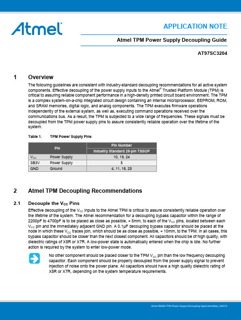
Atmel-8580B-TPM-Power-Supply-Decoupling-ApplicationNote_042014APPLICATION NOTE Atmel TPM Power Supply Decoupling GuideAT97SC32041 OverviewThe following guidelines are consistent with industry-standard decoupling recommendations for all active system components. Effective decoupling of the power supply inputs to the Atmel ® Trusted Platform Module (TPM) is critical to assuring reliable component performance in a high-density printed circuit board environment. The TPM is a complex system-on-a-chip integrated circuit design containing an internal microprocessor, EEPROM, ROM, and SRAM memories, digital logic, and analog components. The TPM executes firmware operationsindependently of the external system, as well as, executing command operations received over thecommunications bus. As a result, the TPM is subjected to a wide range of frequencies. These signals must be decoupled from the TPM power supply pins to assure consistently reliable operation over the lifetime of the system.Table 1. TPM Power Supply Pins2Atmel TPM Decoupling Recommendations 2.1 Decouple the V CC PinsEffective decoupling of the V CC inputs to the Atmel TPM is critical to assure consistently reliable operation over the lifetime of the system. The Atmel recommendation for a decoupling bypass capacitor within the range of 2200pF to 4700pF is to be placed as close as possible, < 5mm, to each of the V CC pins, located between each V CC pin and the immediately adjacent GND pin. A 0.1μF decoupling bypass capacitor should be placed at the node in which these V CC traces join, which should be as close as possible, < 10mm, to the TPM. In all cases, this bypass capacitor should be closer than the next closest component. All capacitors should be of high quality, with dielectric ratings of X5R or X7R. A low-power state is automatically entered when the chip is idle. No further action is required by the system to enter low-power mode.No other component should be placed closer to the TPM V CC pin than the low frequency decoupling capacitor. Each component should be properly decoupled from the power supply signal to prevent injection of noise onto the power plane. All capacitors should have a high quality dielectric rating of X5R or X7R, depending on the system temperature requirements.2.2 Decouple the SBV3 PinIn order to decouple the SB3V pin, it is recommended that a decoupling capacitor, no smaller than 2200pF and no larger than 4700pF, be placed as near as possible to the SB3V pin, located between the SB3V pin and the immediately adjacent GND pin in order to address high frequency noise. The placement should be less than 5mm from the SB3V pin; although, best performance is achieved when the capacitor is placed directly next to the chip leads. Chip capacitors of size 0402 will fit well between board traces for the 28-pin TSSOP.A second 0.1µF decoupling bypass capacitor should be placed between the SB3V pin and the Supply rail, whichshould be as close as possible (< 10mm) to the TPM. This capacitor will address lower frequency supply noise.No other component should be placed closer to the TPM SB3V pin than the low frequency decouplingcapacitor. Each component should be properly decoupled from the power supply signal to preventinjection of noise onto the power plane. Both capacitors should have a high quality dielectric rating ofX5R or X7R, depending on the system temperature requirements.2.3 Decoupling DiagramsThe below figures illustrate power and ground pins only.Figure 2-1. 28-pin TSSOP3TPM Power Supply Decoupling Guide [APPLICATION NOTE]2Atmel-8580B-TPM-Power-Supply-Decoupling-ApplicationNote_042014。
全新SAM3N系列微控制器(Atmel)

全新SAM3N系列微控制器(Atmel)爱特梅尔公司(Atmel®Corporation)推出全新SAM3N 系列微控制器,扩展其ARM®Cortex™-M3 Flash 系列。
新推出的SAM3N 系列是瞄准消费、工业控制、计量、玩具、医疗、测试和测量、802.15.4 无线网络,以及PC、手机与游戏外设等应用的通用型微控制器,具有高性能、低功耗、可扩展存储器、低引脚数目、封装可选及支持电容式触摸优势。
SAM3N 系列产品拥有开发工具、软件,系统内编程功能,以及来自ARM 第三方生态系统网络的支持,兼具高性能和使用简便的优势。
爱特梅尔SAM3N 和SAM3S 系列是首款可提供按键、滑块和转盘的电容式触摸支持的ARM-based 微控制器,用户可利用爱特梅尔QTouch®软件库和Studio 设计工具来部署先进用户接口。
新产品系列能够提供1.62V 至3.6V 的更大供电电压范围,实现真正的1.8V 运作,且工作模式下功耗/MHz 仅为0.86mW。
在实时时钟(RTC)运行的1.8V 待机模式下,耗电量更可降至1.9uA。
爱特梅尔SAM3N Cortex-M3 Flash 系列与爱特梅尔最畅销的ARM7TDMI®- based SAM7S 系列引脚完全兼容,提供了提高性能、降低功耗的理想移植途径。
SAM3N 系列通过降低价位,以及采用片上端接电阻以提高系统级集成度来优化总体材料清单(BOM)。
爱特梅尔公司ARM 微控制器产品总监Jacko Wilbrink 称:“SAM3N系列是具有最佳成本与功耗、处理能力与外设集比率的理想的通用型微控制器。
而SAM3S 系列则提供额外的功能、更高的性能和更多的外设选择,包括12 位ADC、SDIO、USB 全速器件、外部总线接口和更多Flash SRAM 选项。
”SAM3N 系列是爱特梅尔基于高性能32 位ARM Cortex-M3 RISC 处理器的Flash 微控制器系列的成员。
atmel单片机参数
atmel单片机参数Atmel单片机参数引言:Atmel是一家知名的微控制器制造商,其单片机产品系列广泛应用于各种电子设备中。
本文将介绍Atmel单片机的一些重要参数,包括架构、时钟频率、存储器容量、输入输出接口等,以帮助读者更好地了解和选择合适的Atmel单片机产品。
一、架构(Architecture)Atmel单片机采用了先进的RISC架构(Reduced Instruction Set Computer),这种架构具有指令集精简、指令执行速度快等特点。
RISC架构的设计使得Atmel单片机在相同主频下能够执行更多的指令,提高了系统的性能和效率。
二、时钟频率(Clock Frequency)Atmel单片机的时钟频率是指单片机内部时钟的运行速度,通常以MHz(兆赫兹)为单位。
时钟频率越高,单片机的运行速度越快,能够处理更复杂的任务。
在选择Atmel单片机时,我们需要根据具体应用的需求来确定合适的时钟频率。
三、存储器容量(Memory Capacity)Atmel单片机具有不同的存储器类型和容量,包括闪存(Flash)、随机存取存储器(RAM)和电子可擦除可编程只读存储器(EEPROM)。
闪存用于存储程序代码,RAM用于存储数据,而EEPROM用于存储非易失性数据。
存储器容量的大小直接影响了单片机能够存储的程序和数据的大小,因此在选择Atmel单片机时需要根据具体应用需求来确定合适的存储器容量。
四、输入输出接口(I/O Interfaces)Atmel单片机提供了丰富的输入输出接口,包括通用输入输出(GPIO)、模拟输入输出(ADC/DAC)、串行通信接口(UART/SPI/I2C)等。
这些接口可以与外部设备进行数据交换,实现与外界的通信和控制。
在选择Atmel单片机时,我们需要根据具体应用的需求来确定所需的输入输出接口类型和数量。
五、功耗(Power Consumption)Atmel单片机具有低功耗特性,能够在不同的功耗模式下灵活运行。
ATMEL单片机程序烧写软件安装教程
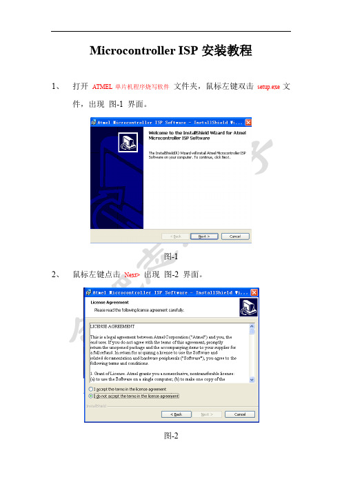
图-2
3、选中第一项,如图-3所示,再用鼠标左键点击Next>,然后填入个人信息如图-4界面。
图-3
图-4
4、用鼠标左键点击Next>,出现图-5界面
界面
图-6
6、用鼠标左键点击Install,出现图-7界面,系统开始安装,安装完成出现图-8界面。
图3图4用鼠标左键点击next出现图5界面图5用鼠标左键点击next出现图6界面图6用鼠标左键点击install出现图7界面系统开始安装安装完成出现图8界面
Microcontroller ISP安装教程
1、打开ATMEL单片机程序烧写软件文件夹,鼠标左键双击setup.exe文件,出现图-1界面。
图-1
图-7
图-8
7、用鼠标左键点击Finish,出现图-9界面
图-9
8、用鼠标左键点击Yes,重启电脑后我们就可以使用这个烧写软件了。
