Dynamic Ordering for Asynchronous Backtracking on
USB Type-C 规范1.2(中文版)

知识产权声明
THIS SPECIFICATION IS PROVIDED TO YOU “AS IS” WITH NO WARRANTIES WHATSOEVER, INCLUDING ANY WARRANTY OF MERCHANTABILITY, NON-INFRINGEMENT, OR FITNESS FOR ANY PARTICULAR PURPOSE. THE AUTHORS OF THIS SPECIFICATION DISCLAIM ALL LIABILITY, INCLUDING LIABILITY FOR INFRINGEMENT OF ANY PROPRIETARY RIGHTS, RELATING TO USE OR IMPLEMENTATION OF INFORMATION IN THIS SPECIFICATION. THE PROVISION OF THIS SPECIFICATION TO YOU DOES NOT PROVIDE YOU WITH ANY LICENSE, EXPRESS OR IMPLIED, BY ESTOPPEL OR OTHERWISE, TO ANY INTELLECTUAL PROPERTY RIGHTS.
预发行行业审查公司提供反馈
Revision History.......................................................................................................................14
LIMITED COPYRIGHT LICENSE: The USB 3.0 Promoters grant a conditional copyright license under the copyrights embodied in the USB Type-C Cable and Connector Specification to use and reproduce the Specification for the sole purpose of, and solely to the extent necessary for, evaluating whether to implement the Specification in products that would comply with the specification.
低频活动漂浮潜水船声探测系统(LFATS)说明书

LOW-FREQUENCY ACTIVE TOWED SONAR (LFATS)LFATS is a full-feature, long-range,low-frequency variable depth sonarDeveloped for active sonar operation against modern dieselelectric submarines, LFATS has demonstrated consistent detection performance in shallow and deep water. LFATS also provides a passive mode and includes a full set of passive tools and features.COMPACT SIZELFATS is a small, lightweight, air-transportable, ruggedized system designed specifically for easy installation on small vessels. CONFIGURABLELFATS can operate in a stand-alone configuration or be easily integrated into the ship’s combat system.TACTICAL BISTATIC AND MULTISTATIC CAPABILITYA robust infrastructure permits interoperability with the HELRAS helicopter dipping sonar and all key sonobuoys.HIGHLY MANEUVERABLEOwn-ship noise reduction processing algorithms, coupled with compact twin line receivers, enable short-scope towing for efficient maneuvering, fast deployment and unencumbered operation in shallow water.COMPACT WINCH AND HANDLING SYSTEMAn ultrastable structure assures safe, reliable operation in heavy seas and permits manual or console-controlled deployment, retrieval and depth-keeping. FULL 360° COVERAGEA dual parallel array configuration and advanced signal processing achieve instantaneous, unambiguous left/right target discrimination.SPACE-SAVING TRANSMITTERTOW-BODY CONFIGURATIONInnovative technology achievesomnidirectional, large aperture acousticperformance in a compact, sleek tow-body assembly.REVERBERATION SUPRESSIONThe unique transmitter design enablesforward, aft, port and starboarddirectional transmission. This capabilitydiverts energy concentration away fromshorelines and landmasses, minimizingreverb and optimizing target detection.SONAR PERFORMANCE PREDICTIONA key ingredient to mission planning,LFATS computes and displays systemdetection capability based on modeled ormeasured environmental data.Key Features>Wide-area search>Target detection, localization andclassification>T racking and attack>Embedded trainingSonar Processing>Active processing: State-of-the-art signal processing offers acomprehensive range of single- andmulti-pulse, FM and CW processingfor detection and tracking. Targetdetection, localization andclassification>P assive processing: LFATS featuresfull 100-to-2,000 Hz continuouswideband coverage. Broadband,DEMON and narrowband analyzers,torpedo alert and extendedtracking functions constitute asuite of passive tools to track andanalyze targets.>Playback mode: Playback isseamlessly integrated intopassive and active operation,enabling postanalysis of pre-recorded mission data and is a keycomponent to operator training.>Built-in test: Power-up, continuousbackground and operator-initiatedtest modes combine to boostsystem availability and accelerateoperational readiness.UNIQUE EXTENSION/RETRACTIONMECHANISM TRANSFORMS COMPACTTOW-BODY CONFIGURATION TO ALARGE-APERTURE MULTIDIRECTIONALTRANSMITTERDISPLAYS AND OPERATOR INTERFACES>State-of-the-art workstation-based operator machineinterface: Trackball, point-and-click control, pull-down menu function and parameter selection allows easy access to key information. >Displays: A strategic balance of multifunction displays,built on a modern OpenGL framework, offer flexible search, classification and geographic formats. Ground-stabilized, high-resolution color monitors capture details in the real-time processed sonar data. > B uilt-in operator aids: To simplify operation, LFATS provides recommended mode/parameter settings, automated range-of-day estimation and data history recall. >COTS hardware: LFATS incorporates a modular, expandable open architecture to accommodate future technology.L3Harrissellsht_LFATS© 2022 L3Harris Technologies, Inc. | 09/2022NON-EXPORT CONTROLLED - These item(s)/data have been reviewed in accordance with the InternationalTraffic in Arms Regulations (ITAR), 22 CFR part 120.33, and the Export Administration Regulations (EAR), 15 CFR 734(3)(b)(3), and may be released without export restrictions.L3Harris Technologies is an agile global aerospace and defense technology innovator, delivering end-to-endsolutions that meet customers’ mission-critical needs. The company provides advanced defense and commercial technologies across air, land, sea, space and cyber domains.t 818 367 0111 | f 818 364 2491 *******************WINCH AND HANDLINGSYSTEMSHIP ELECTRONICSTOWED SUBSYSTEMSONAR OPERATORCONSOLETRANSMIT POWERAMPLIFIER 1025 W. NASA Boulevard Melbourne, FL 32919SPECIFICATIONSOperating Modes Active, passive, test, playback, multi-staticSource Level 219 dB Omnidirectional, 222 dB Sector Steered Projector Elements 16 in 4 stavesTransmission Omnidirectional or by sector Operating Depth 15-to-300 m Survival Speed 30 knotsSize Winch & Handling Subsystem:180 in. x 138 in. x 84 in.(4.5 m x 3.5 m x 2.2 m)Sonar Operator Console:60 in. x 26 in. x 68 in.(1.52 m x 0.66 m x 1.73 m)Transmit Power Amplifier:42 in. x 28 in. x 68 in.(1.07 m x 0.71 m x 1.73 m)Weight Winch & Handling: 3,954 kg (8,717 lb.)Towed Subsystem: 678 kg (1,495 lb.)Ship Electronics: 928 kg (2,045 lb.)Platforms Frigates, corvettes, small patrol boats Receive ArrayConfiguration: Twin-lineNumber of channels: 48 per lineLength: 26.5 m (86.9 ft.)Array directivity: >18 dB @ 1,380 HzLFATS PROCESSINGActiveActive Band 1,200-to-1,00 HzProcessing CW, FM, wavetrain, multi-pulse matched filtering Pulse Lengths Range-dependent, .039 to 10 sec. max.FM Bandwidth 50, 100 and 300 HzTracking 20 auto and operator-initiated Displays PPI, bearing range, Doppler range, FM A-scan, geographic overlayRange Scale5, 10, 20, 40, and 80 kyd PassivePassive Band Continuous 100-to-2,000 HzProcessing Broadband, narrowband, ALI, DEMON and tracking Displays BTR, BFI, NALI, DEMON and LOFAR Tracking 20 auto and operator-initiatedCommonOwn-ship noise reduction, doppler nullification, directional audio。
Slave-Redundancy(从设备冗余的要求)

Prepared by the PROFIBUS Working Group 4 “DCS Requirements” in the Technical Committee 4 “System Integration”.
This revised version V1.2 replaces draft version V1.1. There is one change according a change request based on the PNO review in the informative Annex B "GSD requirements": the requirement for Slave_Redundancy_supp is adjusted to GSD specification V5.02. The major changes to V1.0 are described in the introduction.
The attention of adopters is directed to the possibility that compliance with or adoption of PI (PROFIBUS International) specifications may require use of an invention covered by patent rights. PI shall not be responsible for identifying patents for which a license may be required by any PI specification, or for conducting legal inquiries into the legal validity or scope of those patents that are brought to its attention. PI specifications are prospective and advisory only. Prospective users are responsible for protecting themselves against liability for infringement of patents. NOTICE: The information contained in this document is subject to change without notice. The material in this document details a PI specification in accordance with the license and notices set forth on this page. This document does not represent a commitment to implement any portion of this specification in any company's products. WHILE THE INFORMATION IN THIS PUBLICATION IS BELIEVED TO BE ACCURATE, PI MAKES NO WARRANTY OF ANY KIND, EXPRESS OR IMPLIED, WITH REGARD TO THIS MATERIAL INCLUDING, BUT NOT LIMITED TO ANY WARRANTY OF TITLE OR OWNERSHIP, IMPLIED WARRANTY OF MERCHANTABILITY OR WARRANTY OF FITNESS FOR PARTICULAR PURPOSE OR USE. In no event shall PI be liable for errors contained herein or for indirect, incidental, special, consequential, reliance or cover damages, including loss of profits, revenue, data or use, incurred by any user or any third party. Compliance with this specification does not absolve manufacturers of PROFIBUS or PROFINET equipment, from the requirements of safety and regulatory agencies (TÜV, BIA, UL, CSA, FCC, IECBUS Nutzerorganisation e.V. Haid-und-Neu-Str. 7 D-76131 Karlsruhe Germany Phone: +49 721 / 96 58 590 Fax: +49 721 / 96 58 589 E-mail: pi@ Web site:
使用@Transactional(propagation=Propagation.SUPP。。。

使⽤@Transactional(propagation=Propagation.SUPP。
Spring 的事务传播机制中 Propagation.SUPPORTS 级别的意义是,如果当前环境有事务,就加⼊到当前事务;如果没有事务,就以⾮事务的⽅式执⾏。
从这个说明来看,使⽤这个级别和不加@Transaction注解也没什么不⼀样,找 API 看⼀下,枚举 Propagation 的 SUPPORTS 项如下:Support a current transaction, execute non-transactionally if none exists. Analogous to EJB transaction attribute of the samename.Note: For transaction managers with transaction synchronization, PROPAGATION_SUPPORTS is slightly different from notransaction at all, as it defines a transaction scope that synchronization will apply for. As a consequence, the same resources(JDBC Connection, Hibernate Session, etc) will be shared for the entire specified scope. Note that this depends on the actualsynchronization configuration of the transaction manager.See Also:AbstractPlatformTransactionManager.setTransactionSynchronization(int)除了意义的说明,⽂档中还有⼀个 Note:对于设置了 transaction synchronization 的事务管理器,两种⽅式有微⼩的不同,即使⽤@Transactional(propagation = Propagation.SUPPORTS) ⽅式会定义⼀个事务作⽤域,等等… 但是还是没理解有什么⽤,继续看⼀下See 指向的地⽅/*** Set when this transaction manager should activate the thread-bound* transaction synchronization support. Default is "always".* <p>Note that transaction synchronization isn't supported for* multiple concurrent transactions by different transaction managers.* Only one transaction manager is allowed to activate it at any time.* @see #SYNCHRONIZATION_ALWAYS* @see #SYNCHRONIZATION_ON_ACTUAL_TRANSACTION* @see #SYNCHRONIZATION_NEVER* @see TransactionSynchronizationManager* @see TransactionSynchronization*/public final void setTransactionSynchronization(int transactionSynchronization) {this.transactionSynchronization = transactionSynchronization;}也没看出什么,按照See的指⽰,去看 TransactionSynchronization1 package org.springframework.transaction.support;23 import java.io.Flushable;45/**6 * Interface for transaction synchronization callbacks.7 * Supported by AbstractPlatformTransactionManager.8 *9 * <p>TransactionSynchronization implementations can implement the Ordered interface10 * to influence their execution order. A synchronization that does not implement the11 * Ordered interface is appended to the end of the synchronization chain.12 *13 * <p>System synchronizations performed by Spring itself use specific order values,14 * allowing for fine-grained interaction with their execution order (if necessary).15 *16 * @author Juergen Hoeller17 * @since 02.06.200318 * @see TransactionSynchronizationManager19 * @see AbstractPlatformTransactionManager20 * @see org.springframework.jdbc.datasource.DataSourceUtils#CONNECTION_SYNCHRONIZATION_ORDER21*/22public interface TransactionSynchronization extends Flushable {2324/** Completion status in case of proper commit */25int STATUS_COMMITTED = 0;2627/** Completion status in case of proper rollback */28int STATUS_ROLLED_BACK = 1;2930/** Completion status in case of heuristic mixed completion or system errors */31int STATUS_UNKNOWN = 2;323334/**35 * Suspend this synchronization.36 * Supposed to unbind resources from TransactionSynchronizationManager if managing any.37 * @see TransactionSynchronizationManager#unbindResource38*/39void suspend();4041/**42 * Resume this synchronization.43 * Supposed to rebind resources to TransactionSynchronizationManager if managing any.44 * @see TransactionSynchronizationManager#bindResource45*/46void resume();4748/**49 * Flush the underlying session to the datastore, if applicable:50 * for example, a Hibernate/JPA session.51 * @see org.springframework.transaction.TransactionStatus#flush()52*/53 @Override54void flush();5556/**57 * Invoked before transaction commit (before "beforeCompletion").58 * Can e.g. flush transactional O/R Mapping sessions to the database.59 * <p>This callback does <i>not</i> mean that the transaction will actually be committed.60 * A rollback decision can still occur after this method has been called. This callback61 * is rather meant to perform work that's only relevant if a commit still has a chance62 * to happen, such as flushing SQL statements to the database.63 * <p>Note that exceptions will get propagated to the commit caller and cause a64 * rollback of the transaction.65 * @param readOnly whether the transaction is defined as read-only transaction66 * @throws RuntimeException in case of errors; will be <b>propagated to the caller</b>67 * (note: do not throw TransactionException subclasses here!)68 * @see #beforeCompletion69*/70void beforeCommit(boolean readOnly);7172/**73 * Invoked before transaction commit/rollback.74 * Can perform resource cleanup <i>before</i> transaction completion.75 * <p>This method will be invoked after {@code beforeCommit}, even when76 * {@code beforeCommit} threw an exception. This callback allows for77 * closing resources before transaction completion, for any outcome.78 * @throws RuntimeException in case of errors; will be <b>logged but not propagated</b>79 * (note: do not throw TransactionException subclasses here!)80 * @see #beforeCommit81 * @see #afterCompletion82*/83void beforeCompletion();8485/**86 * Invoked after transaction commit. Can perform further operations right87 * <i>after</i> the main transaction has <i>successfully</i> committed.88 * <p>Can e.g. commit further operations that are supposed to follow on a successful89 * commit of the main transaction, like confirmation messages or emails.90 * <p><b>NOTE:</b> The transaction will have been committed already, but the91 * transactional resources might still be active and accessible. As a consequence,92 * any data access code triggered at this point will still "participate" in the93 * original transaction, allowing to perform some cleanup (with no commit following94 * anymore!), unless it explicitly declares that it needs to run in a separate95 * transaction. Hence: <b>Use {@code PROPAGATION_REQUIRES_NEW} for any96 * transactional operation that is called from here.</b>97 * @throws RuntimeException in case of errors; will be <b>propagated to the caller</b>98 * (note: do not throw TransactionException subclasses here!)99*/100void afterCommit();101102/**103 * Invoked after transaction commit/rollback.104 * Can perform resource cleanup <i>after</i> transaction completion.105 * <p><b>NOTE:</b> The transaction will have been committed or rolled back already, 106 * but the transactional resources might still be active and accessible. As a107 * consequence, any data access code triggered at this point will still "participate"108 * in the original transaction, allowing to perform some cleanup (with no commit109 * following anymore!), unless it explicitly declares that it needs to run in a110 * separate transaction. Hence: <b>Use {@code PROPAGATION_REQUIRES_NEW} 111 * for any transactional operation that is called from here.</b>112 * @param status completion status according to the {@code STATUS_*} constants113 * @throws RuntimeException in case of errors; will be <b>logged but not propagated</b> 114 * (note: do not throw TransactionException subclasses here!)115 * @see #STATUS_COMMITTED116 * @see #STATUS_ROLLED_BACK117 * @see #STATUS_UNKNOWN118 * @see #beforeCompletion119*/120void afterCompletion(int status);121122 }从这看出点意思, spring 框架执⾏事务的过程中可以执⾏回调。
WM8994__Natertech

wDESCRIPTIONThe WM8994 is a highly integrated ultra-low power hi-fi CODEC designed for smartphones and other portable devices rich in multimedia features. An integrated stereo class D/AB speaker driver and class W headphone driver minimize power consumption during audio playback. The device requires only two voltage supplies, with all other internal supply rails generated from integrated LDOs. Stereo full duplex asynchronous sample rate conversion and multi-channel digital mixing combined with powerful analogue mixing allow the device to support a huge range of different architectures and use cases. A fully programmable parametric EQ provides speaker compensation and a dynamic range controller can be used in the ADC or DAC paths for maintaining a constant signal level, maximizing loudness and protecting speakers against overloading and clipping. A smart digital microphone interface provides power regulation, a low jitter clock output and decimation filters for up to four digital microphones. A MIC activity detect with interrupt is available. Active ground loop noise rejection and DC offset correction help prevent pop noise and suppress ground noise on the headphone outputs.WM8994Multi-Channel Audio Hub CODEC for SmartphonesFEATURES• • • Hi-Fi 24-bit 4-channel DAC and 2-channel ADC 100dB SNR during DAC playback (‘A’ weighted) Smart MIC interface - Power, clocking and data input for up to four digital MICs - High performance analogue MIC interface - MIC activity monitor & interrupt allows processor to sleep 1W stereo / 2W mono class D/AB speaker driver Capless Class W headphone drivers - Integrated charge pump - 5.3mW total power for DAC playback to headphones 4 Line outputs (single-ended or differential) BTL Earpiece driver Digital audio interfaces for multi-processor architecture - Asynchronous stereo duplex sample rate conversion - Powerful mixing and digital loopback functions ReTuneTM Mobile 5-band, 6-channel parametric EQ Programmable dynamic range controller Dual FLL provides all necessary clocks - Self-clocking modes allow processor to sleep - All standard sample rates from 8kHz to 96kHz Active noise reduction circuits - DC offset correction removes pops and clicks - Ground loop noise cancellation Integrated LDO regulators 72-ball W-CSP package (4.511 x 4.023 x 0.7mm)• • • • • • • • • • •APPLICATIONS• • • • • Smartphones and music phones Portable navigation Tablets eBooks Portable Media PlayersWOLFSON MICROELECTRONICS plcTo receive regular email updates, sign up at /enewsProduct Brief, November 2010, Rev 3.0Copyright ©2010 Wolfson Microelectronics plcWM8994 PIN CONFIGURATION1 A 2 3 4 5 6LINEOUT FBProduct Brief78IN2RP/ VRXP9IN2RN/ DMICDAT 2SPKGND1CIFMODEREFGNDMICBIAS1BSPKOUT RPLINEOUT 2PLINEOUT 1PMICBIAS2IN1RNIN2LP/ VRXNIN2LN/ DMICDAT 1CSPKGND2SPKVDD2SPKOUT RNLINEOUT 2NLINEOUT 1NDMICCLKIN1RPIN1LPVMIDCDLDO2VDDDBVDDMCLK1LDO1ENALDO2ENAAGNDIN1LNAVDD2AVDD1EGPIO2/ MCLK2DGNDLRCLK1DACDAT1GPIO7/ ADCDAT2VREFCAGNDAGNDLDO1VDDFDCVDDADCDAT1SDAGPIO4/ LRCLK2GPIO9/ ADCDAT3GPIO11/ BCLK3HP2GNDHPOUT2PHPOUT2NGBCLK1CS/ADDRADC LRCLK1/ GPIO1GPIO6/ ADC LRCLK2HPOUT1RCPVOUTPCPCACPVDDHSCLKGPIO3/ BCLK2GPIO5/ DACDAT2GPIO8/ DACDAT3GPIO10/ LRCLK3HPOUT1LCPVOUTNCPCBCPGNDORDERING INFORMATIONORDER CODE WM8994ECS/R Note: Reel quantity = 3500 TEMPERATURE RANGE -40°C to +85°C PACKAGE 72-ball W-CSP (Pb-free, Tape and reel) MOISTURE SENSITIVITY LEVEL MSL1 PEAK SOLDERING TEMPERATURE 260°CwProduct Brief, November 2010, Rev 3.0 2Product BriefWM8994PIN DESCRIPTIONPIN NO A1 A2 A3 A4 A5 A6 A7 A8 NAME SPKGND1 SPKOUTLP SPKMODE CIFMODE REFGND LINEOUTFB MICBIAS1 IN2RP/VRXP Supply Analogue Output Digital Input Digital Input Supply Analogue Input Analogue Output Analogue Input TYPE Left speaker positive output 2W Mono/1W Stereo speaker mode select Selects 2-wire or 3/4-wire control interface mode Analogue ground Line output ground loop noise rejection feedback Microphone bias 1 Left channel line input / Left channel positive differential MIC input / Mono differential positive input (RXVOICE +) Right channel line input / Right channel negative differential MIC input / Left speaker negative output Supply for speaker driver 1 (Left channel) Right speaker positive output Positive mono line output / Positive left line output Positive mono line output / Positive left line output Microphone bias 2 Right channel single-ended MIC input / Right channel negative differential MIC input Left channel line input / Left channel positive differential MIC input / Mono differential negative input (RXVOICE -) Left channel line input / Left channel negative differential MIC input / Digital MIC data input 1 Ground for speaker driver (Return path for SPKVDD2) Supply for speaker driver 2 (Right channel) Right speaker negative output Negative mono line output / Positive left or right line output Negative mono line output / Positive left or right line output Digital MIC clock output Right channel line input / Right channel positive differential MIC input Left channel line input / Left channel positive differential MIC input Midrail voltage decoupling capacitor Supply for LDO2 Digital buffer (I/O) supply Master clock 1 Enable pin for LDO1 Enable pin for LDO2 Analogue ground (Return path for AVDD1) Left channel single-ended MIC input / Left channel negative differential MIC input Bandgap reference, analogue class D and FLL supply Analogue core supply / LDO1 Output General Purpose pin GPI 2 / Master clock 2 Digital ground (Return path for DCVDD and DBVDD) Audio interface 1 left / right clock Product Brief, November 2010, Rev 3.0 3 DESCRIPTION Ground for speaker driver (Return path for SPKVDD1)A9 B1 B2 B3 B4 B5 B6 B7 B8IN2RN/ DMICDAT2 SPKOUTLN SPKVDD1 SPKOUTRP LINEOUT2P LINEOUT1P MICBIAS2 IN1RN IN2LP/VRXNAnalogue Input / Digital Input Analogue Output Supply Analogue Output Analogue Output Analogue Output Analogue Output Analogue Input Analogue InputB9IN2LN/ DMICDAT1 SPKGND2 SPKVDD2 SPKOUTRN LINEOUT2N LINEOUT1N DMICCLK IN1RP IN1LP VMIDC LDO2VDD DBVDD MCLK1 LDO1ENA LDO2ENA AGND IN1LN AVDD2 AVDD1 GPIO2/ MCLK2 DGND LRCLK1Analogue Input / Digital Input Supply Supply Analogue Output Analogue Output Analogue Output Digital Output Analogue Input Analogue Input Analogue Output Supply Supply Digital Input Digital Input Digital Input Supply Analogue Input Supply Supply / Analogue Output Digital Input Supply Digital Input / OutputC1 C2 C3 C4 C5 C6 C7 C8 C9 D1 D2 D3 D4 D5 D6 D7 D8 D9 E1 E2 E3wWM8994PIN NO E4 E5 E6 E7 E8 E9 F1 F2 F3 F4 F5 F6 F7 F8 F9 G1 G2 G3 NAME DACDAT1 GPIO7/ ADCDAT2 VREFC AGND AGND LDO1VDD DCVDD ADCDAT1 SDA GPIO4/ LRCLK2 GPIO9/ ADCDAT3 GPIO11/ BCLK3 HP2GND HPOUT2P HPOUT2N BCLK1 CS/ADDR ¯¯ ADCLRCLK1/ GPIO1 GPIO6/ ADCLRCLK2 HPOUT1FB HPOUT1R CPVOUTP CPCA CPVDD SCLK GPIO3/ BCLK2 GPIO5/ DACDAT2 GPIO8/ DACDAT3 GPIO10/ LRCLK3 HPOUT1L CPVOUTN CPCB CPGND TYPE Digital Input Digital Input / Output Analogue Output Supply Supply Supply Supply / Analogue Output Digital Output Digital Input / Output Digital Input / Output Digital Input / Output Digital Input / Output Supply Analogue Output Analogue Output Digital Input / Output Digital Input Digital Input / Output DESCRIPTION Audio interface 1 DAC digital audio data General Purpose pin GPIO 7 / Audio interface 2 ADC digital audio data Bandgap reference decoupling capacitor Analogue ground (Return path for AVDD1) Analogue ground (Return path for AVDD1) Supply for LDO1 Digital core supply / LDO2 output Audio interface 1 ADC digital audio dataProduct BriefControl interface data input and output / 2-wire acknowledge output General Purpose pin GPIO 4 / Audio interface 2 left / right clock General Purpose pin GPIO 9 / Audio interface 3 ADC digital audio data General Purpose pin GPIO 11 / Audio interface 3 bit clock Analogue ground Earpiece speaker non-inverted output Earpiece speaker inverted output Audio interface 1 bit clock 3-/4-wire (SPI) chip select or 2-wire (I2C) address select Audio interface 1 ADC left / right clock / General Purpose pin GPIO 1/ Control interface data output General Purpose pin GPIO 6 / Audio interface 2 ADC left / right clock HPOUT1L and HPOUT1R ground loop noise rejection feedback Right headphone output Charge pump positive supply decoupling pin (HPOUT1L, HPOUT1R) Charge pump fly-back capacitor pin Charge pump supply Control interface clock input General Purpose pin GPIO 3 / Audio interface 2 bit clock General Purpose pin GPIO 5 / Audio interface 2 DAC digital audio data General Purpose pin GPIO 8 / Audio interface 3 DAC digital audio data General Purpose pin GPIO 10 / Audio interface 3 left / right clock Left headphone output Charge pump negative supply decoupling pin (HPOUT1L, HPOUT1R) Charge pump fly-back capacitor pin Charge pump ground (Return path for CPVDD)G4 G5 G6 G7 G8 G9 H1 H2 H3 H4 H5 H6 H7 H8 H9Digital Input / Output Analogue Input Analogue Output Analogue Output Analogue Output Supply Digital Input Digital Input / Output Digital Input / Output Digital Input / Output Digital Input / Output Analogue Output Analogue Output Analogue Output SupplywProduct Brief, November 2010, Rev 3.0 4Product BriefWM8994ABSOLUTE MAXIMUM RATINGSAbsolute Maximum Ratings are stress ratings only. Permanent damage to the device may be caused by continuously operating at or beyond these limits. Device functional operating limits and guaranteed performance specifications are given under Electrical Characteristics at the test conditions specified. ESD Sensitive Device. This device is manufactured on a CMOS process. It is therefore generically susceptible to damage from excessive static voltages. Proper ESD precautions must be taken during handling and storage of this device. Wolfson tests its package types according to IPC/JEDEC J-STD-020B for Moisture Sensitivity to determine acceptable storage conditions prior to surface mount assembly. These levels are: MSL1 = unlimited floor life at <30°C / 85% Relative Humidity. Not normally stored in moisture barrier bag. MSL2 = out of bag storage for 1 year at <30°C / 60% Relative Humidity. Supplied in moisture barrier bag. MSL3 = out of bag storage for 168 hours at <30°C / 60% Relative Humidity. Supplied in moisture barrier bag. The Moisture Sensitivity Level for each package type is specified in Ordering Information. CONDITION Supply voltages (AVDD1, DBVDD) Supply voltages (AVDD2, DCVDD, LDO2VDD) Supply voltages (CPVDD) Supply voltages (SPKVDD1, SPKVDD2, LDO1VDD) Voltage range digital inputs Voltage range analogue inputs Operating temperature range, TA Junction temperature, TJMAX Storage temperature after soldering MIN -0.3V -0.3V -0.3V -0.3V DGND -0.3V AGND -0.3V -40ºC -40ºC -65ºC MAX +4.5V +2.5V +2.2V +7.0V DBVDD +0.3V AVDD1 +0.3V +85ºC +150ºC +150ºCwProduct Brief, November 2010, Rev 3.0 5WM8994 RECOMMENDED OPERATING CONDITIONSPARAMETER Digital supply range (Core) Digital supply range (I/O) Analogue supply 1 range Analogue supply 2 range Charge Pump supply range Speaker supply range LDO1 supply range LDO2 supply range Ground SYMBOL DCVDD DBVDD AVDD1 AVDD2 CPVDD SPKVDD1, SPKVDD2 LDO1VDD LDO2VDD DGND, AGND, CPGND, SPKGND1, SPKGND2, REFGND, HP2GND All supplies 1 MIN 0.95 1.62 2.4 1.71 1.71 2.7 2.7 1.71 TYP 1.0 1.8 3.0 1.8 1.8 5.0 5.0 1.8 0 MAX 2.0 3.6 3.3 2.0 2.0 5.5 5.5 2.0Product BriefUNIT V V V V V V V V VPower supply rise time (notes 6, 7 and 8) Notes: 1. 2. 3. 4. 5. 6. 7.μsAnalogue, digital and speaker grounds must always be within 0.3V of each other. There is no power sequencing requirement; the supplies may be enabled in any order. AVDD1 must be less than or equal to SPKVDD1 and SPKVDD2. When AVDD1 is supplied externally (not from LDO1), the LDO1VDD voltage must be greater than or equal to AVDD1 When DCVDD is supplied externally (not from LDO2), the LDO2VDD voltage must be greater than or equal to DCVDD DCVDD and AVDD1 minimum rise times do not apply when these domains are powered using the internal LDOs. The specified minimum power supply rise times assume a minimum decoupling capacitance of 100nF per pin. However, Wolfson strongly advises that the recommended decoupling capacitors are present on the PCB and that appropriate layout guidelines are observed (see “Applications Information” section). The specified minimum power supply rise times also assume a maximum PCB inductance of 10nH between decoupling capacitor and pin.8.wProduct Brief, November 2010, Rev 3.0 6Product BriefWM8994DEVICE DESCRIPTIONThe WM8994 is a low power, high quality audio codec designed to interface with a wide range of processors and analogue components. A high level of mixed-signal integration in a very small footprint makes it ideal for portable applications such as mobile phones. The analogue circuits of the WM8994 are almost entirely backwards-compatible with the WM8993 with the exception of two additional DAC channels, a dual FLL and two integrated LDO regulators. Three sets of audio interface pins are available in order to provide independent and fully asynchronous connections to multiple processors, typically an application processor, baseband processor and wireless transceiver. Any two of these interfaces can operate totally independently and asynchronously while the third interface can be synchronised to either of the other two and can also provide ultra low power loopback modes to support, for example, wireless headset voice calls. Four digital microphone input channels are available to support advanced multi-microphone applications such as noise cancellation. An integrated microphone activity monitor is available to enable the processor to sleep during periods of microphone inactivity, saving power. Four DAC channels are available to support use cases requiring up to four simultaneous digital audio streams to the output drivers. Eight highly flexible analogue inputs allow interfacing to up to four microphone inputs (single-ended or differential), plus multiple stereo or mono line inputs. Connections to an external voice CODEC, FM radio, line input, handset MIC and headset MIC are all fully supported. Signal routing to the output mixers and within the CODEC has been designed for maximum flexibility to support a wide variety of usage modes. A ‘Direct Voice’ path from a voice CODEC directly to the Speaker or Earpiece output drivers is included. Nine analogue output drivers are integrated, including a stereo pair of high power, high quality Class D/AB switchable speaker drivers; these can support 1W each in stereo mode, or can be coupled to support a 2W mono speaker output. A mono earpiece driver is provided, providing output from the output mixers or from the low-power differential ‘Direct Voice’ path. One pair of ground-reference headphone outputs is provided; these are powered from an integrated Charge Pump, enabling high quality, power efficient headphone playback without any requirement for DC blocking capacitors. A DC Servo circuit is available for DC offset correction, thereby suppressing pops and reducing power consumption. Four line outputs are provided, with multiple configuration options including 4 x single-ended output or 2 x differential outputs. The line outputs are suitable for output to a voice CODEC, an external speaker driver or line output connector. Ground loop feedback is available on the headphone outputs and the line outputs, providing rejection of noise on the ground connections. All outputs have integrated pop and click suppression features. Internal differential signal routing and amplifier configurations have been optimised to provide the highest performance and lowest possible power consumption for a wide range of usage scenarios, including voice calls and music playback. The speaker drivers offer low leakage and high PSRR; this enables direct connection to a Lithium battery. The speaker drivers provide eight levels of AC and DC gain to allow output signal levels to be maximised for many commonly-used SPKVDD/AVDD1 combinations. The ADCs and DACs are of hi-fi quality, using a 24-bit low-order oversampling architecture to deliver optimum performance. A flexible clocking arrangement supports mixed sample rates, whilst an integrated ultra-low power dual FLL provides additional flexibility. A high pass filter is available in all ADC and digital MIC paths for removing DC offsets and suppressing low frequency noise such as mechanical vibration and wind noise. A digital mixing path from the ADC or digital MICs to the DAC provides a sidetone of enhanced quality during voice calls. DAC soft mute and un-mute is available for pop-free music playback. The integrated Dynamic Range Controllers (DRC) and ReTuneTM Mobile 5-band parametric equaliser (EQ) provide further processing capability of the digital audio paths. The DRC provides compression and signal level control to improve the handling of unpredictable signal levels. ‘Anti-clip’ and ‘quick release’ algorithms improve intelligibility in the presence of transients and impulsive noises. The EQ provides the capability to tailor the audio path according to the frequency characteristics of an earpiece or loudspeaker, and/or according to user preferences.wProduct Brief, November 2010, Rev 3.0 7WM8994Product Brief The WM8994 has highly flexible digital audio interfaces, supporting a number of protocols, including I2S, DSP, MSB-first left/right justified, and can operate in master or slave modes. PCM operation is supported in the DSP mode. A-law and μ-law companding are also supported. Time division multiplexing (TDM) is available to allow multiple devices to stream data simultaneously on the same bus, saving space and power. The four digital MIC and ADC channels and four DAC channels are available via four TDM channels on Digital Audio Interface 1 (AIF1). A powerful digital mixing core allows data from each TDM channel of each audio interface and from the ADCs and digital MICs to be mixed and re-routed back to a different audio interface and to the 4 DAC output channels. The digital mixing core can operate synchronously with either Audio Interface 1 or Audio Interface 2, with asynchronous stereo full duplex sample rate conversion performed on the other audio interface as required. The system clock (SYSCLK) provides clocking for the ADCs, DACs, DSP core, digital audio interface and other circuits. SYSCLK can be derived directly from one of the MCLK1 or MCLK2 pins or via one of two integrated FLLs, providing flexibility to support a wide range of clocking schemes. Typical portable system MCLK frequencies, and sample rates from 8kHz to 96kHz are all supported. Automatic configuration of the clocking circuits is available, derived from the sample rate and from the MCLK / SYSCLK ratio. The WM8994 uses a standard 2, 3 or 4-wire control interface, providing full software control of all features, together with device register readback. An integrated Control Write Sequencer enables automatic scheduling of control sequences; commonly-used signal configurations may be selected using ready-programmed sequences, including time-optimised control of the WM8994 pop suppression features. It is an ideal partner for a wide range of industry standard microprocessors, controllers and DSPs. Unused circuitry can be disabled under software control, in order to save power; low leakage currents enable extended standby/off time in portable battery-powered applications. Versatile GPIO functionality is provided, with support for button/accessory detect inputs, or for clock, system status, or programmable logic level output for control of additional external circuitry. Interrupt logic, status readback and de-bouncing options are supported within this functionality.wProduct Brief, November 2010, Rev 3.0 8Product BriefWM8994RECOMMENDED EXTERNAL COMPONENTSwProduct Brief, November 2010, Rev 3.0 9WM8994 PACKAGE DIMENSIONSB: 72 BALL W-CSP PACKAGE 4.511 X 4.023 X 0.7 mm BODY, 0.50 mm BALL PITCHDETAIL 12 G A2 A B C D E F G H e D1 2X 2X 0.10 Z 0.10 Z 4 A 9 8 7 6 5 4 3 2 1 D 6Product BriefDM068.CA1 CORNERe 5E1EDETAIL 2TOP VIEWBOTTOM VIEWf1 SOLDER BALLbbb Zf2h 1 Z A1DETAIL 2Symbols A A1 A2 D D1 E E1 e f1 f2 g h 0.035 MIN 0.615 0.219 0.361 4.471 3.983Dimensions (mm) NOM MAX 0.7 0.785 0.244 0.269 0.411 0.386 4.511 4.551 4.00 BSC 4.063 4.023 3.50 BSC 0.50 BSC0.2555 BSC 0.2615 BSCNOTE5 8 90.070 0.314 BSC0.105NOTES: 1. PRIMARY DATUM -Z- AND SEATING PLANE ARE DEFINED BY THE SPHERICAL CROWNS OF THE SOLDER BALLS. 2. THIS DIMENSION INCLUDES STAND-OFF HEIGHT ‘A1’ AND BACKSIDE COATING. 3. A1 CORNER IS IDENTIFIED BY INK/LASER MARK ON TOP PACKAGE. 4. BILATERAL TOLERANCE ZONE IS APPLIED TO EACH SIDE OF THE PACKAGE BODY. 5. ‘e’ REPRESENTS THE BASIC SOLDER BALL GRID PITCH. 6. THIS DRAWING IS SUBJECT TO CHANGE WITHOUT NOTICE. 7. FOLLOWS JEDEC DESIGN GUIDE MO-211-C. 8. f1 = NOMINAL DISTANCE OF BALL CENTRE TO DIE EDGE X AXIS (AS PER POD) – APPLICABLE TO ALL CORNERS OF DIE. 9. f2 = NOMINAL DISTANCE OF DIE CENTRE TO DIE EDGE IN Y AXIS (AS PER POD) – APPLICABLE TO ALL CORNERS OF DIE.wProduct Brief, November 2010, Rev 3.0 10Product Brief WM8994 IMPORTANT NOTICEWolfson Microelectronics plc (“Wolfson”) products and services are sold subject to Wolfson’s terms and conditions of sale, delivery and payment supplied at the time of order acknowledgement.Wolfson warrants performance of its products to the specifications in effect at the date of shipment. Wolfson reserves theright to make changes to its products and specifications or to discontinue any product or service without notice. Customers should therefore obtain the latest version of relevant information from Wolfson to verify that the information is current.Testing and other quality control techniques are utilised to the extent Wolfson deems necessary to support its warranty. Specific testing of all parameters of each device is not necessarily performed unless required by law or regulation.In order to minimise risks associated with customer applications, the customer must use adequate design and operating safeguards to minimise inherent or procedural hazards. Wolfson is not liable for applications assistance or customer product design. The customer is solely responsible for its selection and use of Wolfson products. Wolfson is not liable forsuch selection or use nor for use of any circuitry other than circuitry entirely embodied in a Wolfson product.Wolfson’s products are not intended for use in life support systems, appliances, nuclear systems or systems where malfunction can reasonably be expected to result in personal injury, death or severe property or environmental damage.Any use of products by the customer for such purposes is at the customer’s own risk.Wolfson does not grant any licence (express or implied) under any patent right, copyright, mask work right or other intellectual property right of Wolfson covering or relating to any combination, machine, or process in which its products or services might be or are used. Any provision or publication of any third party’s products or services does not constitute Wolfson’s approval, licence, warranty or endorsement thereof. Any third party trade marks contained in this document belong to the respective third party owner.Reproduction of information from Wolfson datasheets is permissible only if reproduction is without alteration and is accompanied by all associated copyright, proprietary and other notices (including this notice) and conditions. Wolfson isnot liable for any unauthorised alteration of such information or for any reliance placed thereon.Any representations made, warranties given, and/or liabilities accepted by any person which differ from those contained inthis datasheet or in Wolfson’s standard terms and conditions of sale, delivery and payment are made, given and/or accepted at that person’s own risk. Wolfson is not liable for any such representations, warranties or liabilities or for any reliance placed thereon by any person.ADDRESS:Wolfson Microelectronics plc26 Westfield RoadEdinburghEH11 2QBUnited KingdomTel :: +44 (0)131 272 7000Fax :: +44 (0)131 272 7001Email :: sales@w Product Brief, November 2010, Rev 3.011。
微塞米Timberwolf音频处理器系列产品ZL38090说明书
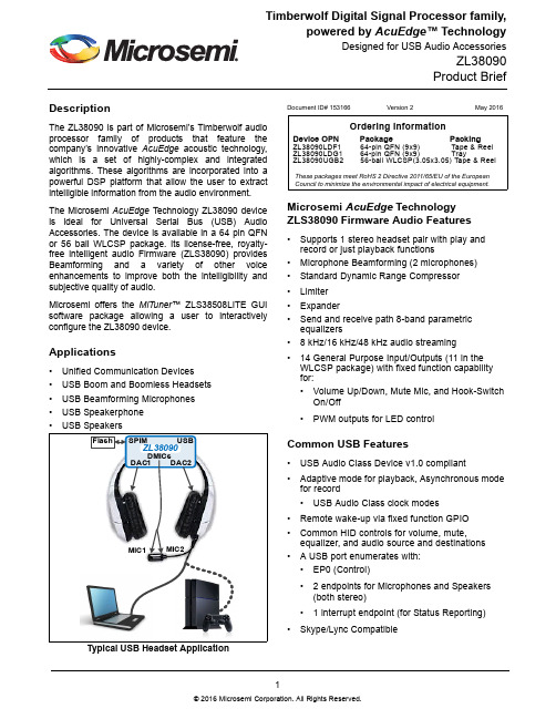
DescriptionThe ZL38090 is part of Microsemi’s Timberwolf audio processor family of products that feature the company’s innovative AcuEdge acoustic technology,which is a set of highly-complex and integrated algorithms. These algorithms are incorporated into a powerful DSP platform that allow the user to extract intelligible information from the audio environment.The Microsemi AcuEdge Technology ZL38090 device is ideal for Universal Serial Bus (USB) Audio Accessories. The device is available in a 64 pin QFN or 56 ball WLCSP package. Its license-free, royalty-free intelligent audio Firmware (ZLS38090) provides Beamforming and a variety of other voice enhancements to improve both the intelligibility and subjective quality of audio.Microsemi offers the MiTuner™ ZLS38508LITE GUI software package allowing a user to interactively configure the ZL38090 device.Applications•Unified Communication Devices •USB Boom and Boomless Headsets •USB Beamforming Microphones •USB SpeakerphoneTypical USB Headset ApplicationZL38090FlashSPIMDAC2DMICs DAC1USBMIC1MIC2Microsemi AcuEdge Technology ZLS38090 Firmware Audio Features•Supports 1 stereo headset pair with play and record or just playback functions•Microphone Beamforming (2 microphones)•Standard Dynamic Range Compressor •Limiter •Expander•Send and receive path 8-band parametric equalizers•8kHz/16kHz/48 kHz audio streaming•14 General Purpose Input/Outputs (11 in the WLCSP package) with fixed function capability for:•Volume Up/Down, Mute Mic, and Hook-Switch On/Off•PWM outputs for LED controlCommon USB Features•USB Audio Class Device v1.0 compliant•Adaptive mode for playback, Asynchronous modefor record •USB Audio Class clock modes •Remote wake-up via fixed function GPIO •Common HID controls for volume, mute, equalizer, and audio source and destinations •A USB port enumerates with:•EP0 (Control)• 2 endpoints for Microphones and Speakers (both stereo)• 1 interrupt endpoint (for Status Reporting)•Skype/Lync CompatibleDocument ID# 153166Version 2May 2016Ordering InformationDevice OPNPackage PackingZL38090LDF1 64-pin QFN (9x9) Tape & Reel ZL38090LDG1 64-pin QFN (9x9) TrayZL38090UGB2 56-ball WLCSP(3.05x3.05) Tape & ReelThese packages meet RoHS 2 Directive 2011/65/EU of the European Council to minimize the environmental impact of electrical equipment.Designed for USB Audio AccessoriesZL38090Product Brief•Stand alone USB device (additional host processor not required for headphoneapplications)ZL38090 Common Hardware Features•DSP with Voice Hardware Accelerators•Dual 16-bit digital-to-analog converters (DAC) •Sampling up to 48kHz and internal output drivers•Headphone amplifiers capable of 32mW output drive power into 16ohms•Impulse pop/click protection• 2 Digital Microphone inputs•TDM port shared between PCM andInter-IC Sound (I2S)•General purpose UART port for debug•Boots from SPI or Flash•Master SPI port for serial Flash interface•Can run unattended (controllerless), self-booting into a configured operational stateFor ease of mounting, the ZL38090 is available in two packages. QFN Hardware Features•64-pin QFN•9mm by 9mm package size•Headphone amplifiers can be configured as2 differential or 4 single-ended outputs• 4 Fixed Function PWM pins for Vol Up, Vol Down, Mute, and Hook Switch control and status•14 General Purpose Input/Output (GPIO) pins •Internal +1.2V voltage regulatorWLCSP Hardware Features•56-ball Wafer Level Chip Scale Package • 3.05mm by 3.05mm package size •Headphone amplifiers can be configured as2 single-ended outputs• 4 Fixed Function PWM pins for Vol Up, Vol Down, Mute, and Hook Switch control and status•11 General Purpose Input/Output (GPIO) pinsTools•ZLK38000 Evaluation Kit•MiTuner™ ZLS38508LITE GUI software Designed for USB Boom and Boomless HeadsetsZL38090Product BriefZL38090 Audio Processor for USB HeadsetsTypical Headset ApplicationThe ZL38090 functions as a complete USB Audio device. The ZL38090 does not require a separate host processor to operate. It it is designed to meet the Skype Certification/Lync Logo specification for a headset. The USB port can be connected to any computer or gaming system. All device controls can be accessed through the USB port,including a subset of basic functions (preset modes) that can be wired to the GPIO pins to provide volume up/down,mute, or special programmable commands.The ZL38090 has two internal differential headphone speaker amplifiers that can drive stereo signals directly into 16/32ohm headphones.Digital microphones can be connected to the ZL38090 DMIC interface, providing a low noise audio pick-up. The ZL38090 can perform beamforming when two microphones are used. Analog microphones can be used with the addition of an electret microphone pre-amplifier device.The ZL38090 has a TDM port that can be used to route audio, or audio can be routed through the USB port. USB Headset Block DiagramNote: When using the WLCSP package option, the headphone speaker amplifiers (DAC1 and DAC2) have single-ended stereo drive.DAC1DAC2DMIC_IN1DMIC_IN2GPIOZLK38090 Evaluation KitThe ZLK38090 Evaluation Kit includes all the hardware necessary to operate the ZLE38090 Evaluation Board. The Evaluation Board provides a flexible platform to evaluate a ZL38090 Timberwolf Audio Processor device with AcuEdge™ Technology Firmware. Firmware Code for the ZL38090 can be downloaded into the Evaluation Board using the ZLS38000 Firmware Loader software. The ZLE38090 Evaluation Board can then be controlled using the MiTuner™ GUI Lite Software (ZLS38508LITE).Device Pinout (64-Pin QFN) Top ViewPackage Outline (64-Pin QFN)Device Pinout (56-Ball WLCSP) Top ViewStaggered Balls (56-Ball WLCSP) Bottom ViewPackage Outline (56-Ball WLCSP)Device PinoutQFN Pin #WLCSPBall Name Type Description15D6RESET Input Reset. When low the device is in its reset state and all tristate outputswill be in a high impedance state. This input must be high for normaldevice operation.A 10KΩ pull-up resistor is required on this node to DVDD33 if this pinis not continuously driven.Table 1 - Reset Pin DescriptionQFN Pin #WLCSPBall Name Type Description6-DAC1_M Output DAC 1 Minus Output. This is the negative output signal of thedifferential amplifier of the DAC 1.Not available on the WLCSP package.7C7DAC1_P DAC 1 Plus Output. This is the positive output signal of thedifferential amplifier of the DAC 1.9-DAC2_M DAC 2 Minus Output. This is the negative output signal of thedifferential amplifier of the DAC 2.Not available on the WLCSP package.8D7DAC2_P DAC 2 Plus Output. This is the positive output signal of thedifferential amplifier of the DAC 2.12F7CDAC DAC Reference. This node requires capacitive decoupling. 13G7CREF Common Mode Reference. This node requires capacitivedecoupling.Table 2 - DAC Pin DescriptionsQFN Pin #WLCSPBall Name Type Description18H6DMIC_CLK Output Digital Microphone Clock Output. Clock output for digitalmicrophones and digital electret microphone pre-amplifier devices. 19H3DMIC_IN1Input Digital Microphone Input 1. Stereo or mono digital microphoneinput.Tie to VSS if unused.20H2DMIC_IN2Input Digital Microphone Input 2. Stereo or mono digital microphoneinput.Tie to VSS if unused.Table 3 - Microphone Pin DescriptionsQFN Pin #WLCSPBall Name Type Description29E1PCLK/I2S_SCK Input/OutputPCM Clock (Input/Tristate Output). PCLK is equal to the bit rate ofsignals DR/DX. In TDM master mode this clock is an output and inTDM slave mode this clock is an input.I2S Serial Clock (Input/Tristate Output). This is the I2S bit clock. InI2S master mode this clock is an output and drives the bit clock inputof the external slave device’s peripheral converters. In I2S slave modethis clock is an input and is driven from a converter operating inmaster mode.After power-up, this signal defaults to be an input in I2S slave mode.A 100KΩ pull-down resistor is required on this pin to VSS. If this pin isunused, tie the pin to VSS.When driving PCLK/I2S_SCK from a host, one of the followingconditions must be satisfied:1.Host drives PCLK low during reset, or2.Host tri-states PCLK during reset (the 100KΩ resistor will keepPCLK low), or3. Host drives PCLK at its normal frequency30F1FS/I2S_WS Input/OutputPCM Frame Pulse (Input/Tristate Output). This is the TDM framealignment reference. This signal is an input for applications where thePCM bus is frame aligned to an external frame signal (slave mode). Inmaster mode this signal is a frame pulse output.I2S Word Select (Left/Right) (Input/Tristate Output). This is the I2Sleft or right word select. In I2S master mode word select is an outputwhich drives the left/right input of the external slave device’speripheral converters. In I2S slave mode this pin is an input which isdriven from a converter operating in master mode.After power-up, this signal defaults to be an input in I2S slave mode.Tie this pin to VSS if unused.31G1DR/I2S_SDI Input PCM Serial Data Stream Input. This serial data stream operates at PCLK data rates.I2S Serial Data Input. This is the I2S port serial data input.Tie this pin to VSS if unused.32H1DX/I2S_SDO Output PCM Serial Data Stream Output. This serial data stream operates at PCLK data rates.I2S Serial Data Output. This is the I2S port serial data output.Table 4 - TDM and I2S Pin DescriptionQFN Pin #WLCSPBall Name Type Description1A5SM_CLK Output Master SPI Port Clock (Tristate Output). Clock output for the MasterSPI port. Maximum frequency = 8MHz.2A6SM_MISO Input Master SPI Port Data Input. Data input signal for the Master SPI port. 3A7SM_MOSI Output Master SPI Port Data Output (Tristate Output). Data output signalfor the Master SPI port.64A4GPIO_9/SM_CSInput/OutputMaster SPI Port Chip Select (Input Internal Pull-Up/TristateOutput). Chip select output for the Master SPI port.Shared with GPIO_9.Table 5 - Master SPI Port Pin DescriptionsQFN Pin #WLCSPBall Name Type Description50B2UART_RX Input UART (Input). Receive serial data in. This port functions as aperipheral interface for an external controller and supports access tothe internal registers and memory of the device.49C2UART_TX Output UART (Tristate Output). Transmit serial data out. This port functionsas a peripheral interface for an external controller and supports accessto the internal registers and memory of the device.Table 6 - UART Pin DescriptionQFN Pin #WLCSPBall Name Type Description33, 34, 36F4, E4,F3GPIO_[0:2]Input/OutputGeneral Purpose I/O (Input Internal Pull-Down/Tristate Output).These pins can be configured as an input or output and are intendedfor low-frequency signalling.37, 38, 39F2, ,F6GPIO_[3:5]General Purpose I/O (Input Internal Pull-Down/Tristate Output).These pins can be configured as an input or output and are intendedfor low-frequency signaling.GPIO_4 is not available on the WLCSP package.64A4GPIO_9/SM_CSGeneral Purpose I/O (Input Internal Pull-Down/Tristate Output).This pin can be configured as an input or output and is intended for low-frequency signalling.Alternate functionality with SM_CS.Table 7 - GPIO Pin DescriptionsQFN Pin #WLCSPBall Name Type Description41E2GPIO_7Input/Output Hook Switch/Volume Down. Fixed function used to control the hook state and volume down with GPIO[10:13].43D3GPIO_8Microphone/Volume Up. Fixed function used to control the hookstate and volume down with GPIO[10:13].44E3GPIO_10Volume Control/Call State. Fixed function used to control the volumeand indicate the call state with GPIO[7:8].45C3GPIO_11Call Control/Volume State 1. Fixed function used to control the hookswitch (on/off) and control multicolor LEDs for volume indication withGPIO[7:8].47-GPIO_12Volume State 2. Fixed function used to control multicolor LEDs forvolume indication with GPIO[7:8].GPIO_12 is not available on the WLCSP package.48-GPIO_13Volume State 3. Fixed function used to control multicolor LEDs forvolume indication with GPIO[7:8].GPIO_13 is not available on the WLCSP package.Table 8 - Headset Control/IndicatorQFN Pin #WLCSPBall Name Type Description22H7XI Input Crystal Oscillator Input.23F5XO Output Crystal Oscillator Output.Table 9 - Oscillator Pin DescriptionQFN Pin #WLCSPBall Name Type Description25H5USB_DM Input/Output USB Data D- Signal. Carries USB data to/from USB 2.0.26G4USB_RTUNE Tx Resistor Tune. Connect to external 43.2 resistor to VSS.27H4USB_DP USB Data D+ Signal. Carries USB data to/from USB 2.0.40E5GPIO_6USB Resume. This pin is used to sense activity on USB Data D+ toresume from sleep or perform a USB reset. It can be configured asan input or output and are intended for low-frequency signaling.Table 10 - USB Pin DescriptionQFN Pin #WLCSPBall Name Type Description17-EXT_SEL Input VDD +1.2V Select. Select external +1.2 V supply. Tie to DVDD33 ifthe +1.2V supply is to be provided externally. Tie to VSS (0 V) if the+1.2 V supply is to be generated internally.Not available on the WLCSP package.16-VDD12_CTRL Output VDD +1.2 V Control. Analog control line for the voltage regulatorexternal FET when EXT_SEL is tied to VSS. When EXT_SEL is tiedto DVDD33, the VDD12_CTRL pin becomes a CMOS output whichcan drive the shutdown input of an external LDO.Not available on the WLCSP package.4, 14, 24, 42, 58B5, D1,G5, G6DVDD12Power Core Supply. Connect to a +1.2V ±5% supply.Place a 100 nF, 20%, 10 V, ceramic capacitor on each pin decoupledto the VSS plane.5, 21, 35, 46, 51, 59B3, B7,G3DVDD33Power Digital Supply. Connect to a +3.3V ±5% supply.Place a 100 nF, 20%, 10 V, ceramic capacitor on each pin decoupledto the VSS plane.28-DVDD33_XTAL Power Crystal Digital Supply. For designs using a crystal or external oscillator, this pin must be connected to a +3.3V supply sourcecapable of delivering 10mA.For designs that do not use a crystal or external oscillator this pincan be tied to VSS in order to save power.Not available on the WLCSP package.10, 11E7AVDD33Power Analog Supply. Connect to a +3.3V ±5% supply.Place a 100 nF, 20%, 10 V, ceramic capacitor on each pin decoupledto the VSS plane.54B4, B6,D2, D4,E6, G2VSS Ground Ground. Connect to digital ground plane.-ExposedGround Pad Ground Exposed Pad Substrate Connection. Connect to VSS. This pad is at ground potential and must be soldered to the printed circuit boardand connected via multiple vias to a heatsink area on the bottom ofthe board and to the internal ground plane.Not available on the WLCSP package.Table 11 - Supply and Ground Pin DescriptionsQFN Pin #WLCSPBall Name Type Description56, 57, 63A3, C1,C6NC No Connection. These pins are to be left unconnected, do not useas a tie point.Table 12 - No Connect Pin DescriptionsTable 13 - IN0 Pin DescriptionsQFN Pin #WLCSP Ball NameType Description 52, 53, 55, 60, 61, 62A1, A2,B1, C4,C5, D5IN0Input IN0. Tie these pins to Ground.Information relating to products and services furnished herein by Microsemi Corporation or its subsidiaries (collectively “Microsemi”) is believed to be reliable. However, Microsemi assumes no liability for errors that may appear in this publication, or for liability otherwise arising from the application or use of any such information, product or service or for any infringement of patents or other intellectual property rights owned by third parties which may result from such application or use. Neither the supply of such information or purchase of product or service conveys any license, either express or implied, under patents or other intellectual property rights owned by Microsemi or licensed from third parties by Microsemi, whatsoever. Purchasers of products are also hereby notified that the use of product in certain ways or in combination with Microsemi, or non-Microsemi furnished goods or services may infringe patents or other intellectual property rights owned by Microsemi.This publication is issued to provide information only and (unless agreed by Microsemi in writing) may not be used, applied or reproduced for any purpose nor form part of any order or contract nor to be regarded as a representation relating to the products or services concerned. The products, their specifications, services and other information appearing in this publication are subject to change by Microsemi without notice. No warranty or guarantee express or implied is made regarding the capability, performance or suitability of any product or service. Information concerning possible methods of use is provided as a guide only and does not constitute any guarantee that such methods of use will be satisfactory in a specific piece of equipment. It is the user’s responsibility to fully determine the performance and suitability of any equipment using such information and to ensure that any publication or data used is up to date and has not been superseded. Manufacturing does not necessarily include testing of all functions or parameters. These products are not suitable for use in any medical and other products whose failure to perform may result in significant injury or death to the user. All products and materials are sold and services provided subject to Microsemi’s conditions of sale which are available on request.For more information about all Microsemi productsvisit our website atTECHNICAL DOCUMENTATION – NOT FOR RESALE© 2016 Microsemi Corporation. All rights reserved. Microsemi and the Microsemi logo are trademarks of Microsemi Corporation. All other trademarks and service marks are the property of their respective owners.Microsemi Corporation (NASDAQ: MSCC) offers a comprehensive portfolio of semiconductorsolutions for: aerospace, defense and security; enterprise and communications; and industrialand alternative energy markets. Products include mixed-signal ICs, SoCs, and ASICs;programmable logic solutions; power management products; timing and voice processingdevices; RF solutions; discrete components; and systems. Microsemi is headquartered in AlisoViejo, Calif. Learn more at .Microsemi Corporate HeadquartersOne Enterprise, Aliso Viejo CA 92656 USAWithin the USA: +1 (949) 380-6100Sales: +1 (949) 380-6136Fax: +1 (949) 215-4996。
OBCA练习题2

OBCA练习题21. 下列关于备份恢复哪些描述正确? *A、支持租户级别的恢复(正确答案)B、恢复过程包括租户系统表和用户表的 Restore 和 Recover过程C、数据备份指备份基线数据,包括全量备份和增量备份D、日志归档指日志数据的自动归档功能(正确答案)2. 集群扩容和缩容所需数据移动平衡操作由OceanBase自动完成无需用户干预 [判断题] *对(正确答案)错3. 以下哪些是OceanBase集群部署的常见方案? *A、三地四中心B、三地五中心(正确答案)C、2D、两地三中心(正确答案)4. OceanBase是如何避免随机写的? *A、oceanBase是一个准内存数据库的架构,存储又采用LSM Tree的架构,可以有效解决随机写和写放大的问题(正确答案)B、对数据的修改,比如insert、update等,都会先放到内存的MemTable中(正确答案)C、MemTable中的数据像传统数据库那样不定期的进行check point到硬盘中D、通过把增量数据与基线数据进行合并,顺序写入磁盘,可以有效降低写随机写(正确答案)5. 租户逻辑上类似传统数据库的实例,创建完成后,每个租户都将有自己的专属进程。
[判断题] *对错(正确答案)6. 同一个资源单元定义unit config(比如2C8G,或者4C16G等),可以被多个资源池使用。
[判断题] *对(正确答案)错7. 对于存量Oracle业务迁移到OceanBase上需要数据实时同步功能,建议使用哪个工具? [单选题] *A、oCPD、DataXC、 OMS(正确答案)D、ODC8. OCP管理集群时每个受管服务器需要安装OCP agent [判断题] *对(正确答案)错9. OceanBase数据库可以部署在哪些环境中? *A、虚拟化环境(正确答案)B、本地机器(正确答案)C、容器化环境(正确答案)D、云平台(正确答案)10. OceanBase集群灾难恢复等级是多少 [单选题] *A、5B、6(正确答案)C、2D、111. 关于OB原生分布式关系型数据库架构的优势下列描述正确的是? *A、数据高可靠+服务高可用:多副本一致性协议Paxos的工业级实现,个别节点发生故障时保证数据零丢失(RPO=0)和服务快速恢复(RTO<30秒)(正确答案)B、线性扩容随着业务量增加进行扩容(比如线上促销期间),随着业务量减少进行缩容(比如促销后)(正确答案)C、高成本:对硬件要求高,需要使用高端小型机和存储D、灵活的部署方式:支持三中心、五中心、主备等多种部署模式(正确答案)12. Ooenabase数据库已经通过TPC-C测试认证 [判断题] *对(正确答案)错13. OceanBase可以实现动态的扩容和缩容。
接近开关通用参数(英文)
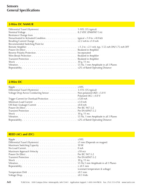
2-Wire DC NAMURDifferential Travel (Hysteresis). . . . . . . . . . . . . . . . . . .1-10% (5% typical)Nominal Voltage. . . . . . . . . . . . . . . . . . . . . . . . . .8.2 VDC (EN60947-5-6)Resistance Change fromNonactivated to Activated Condition. . . . . . . . . . . . . . . .typical <1.0 to >8.0 kΩResulting Current Change. . . . . . . . . . . . . . . . . . . . .≥2.2 mA to≤1.0 mARecommended Switching Point forRemote Amplifier. . . . . . . . . . . . . . . . . . . . . . . . .>1.2 to <2.1 mA, typ. 1.55 mA ON/1.75 mA OFF Power-On Effect. . . . . . . . . . . . . . . . . . . . . . . . . .Realized in AmplifierReverse Polarity Protection. . . . . . . . . . . . . . . . . . . . .IncorporatedWire-Break Protection. . . . . . . . . . . . . . . . . . . . . . .Realized in AmplifierTransient Protection. . . . . . . . . . . . . . . . . . . . . . . .Realized in AmplifierShock. . . . . . . . . . . . . . . . . . . . . . . . . . . . . . .30 g, 11 msVibration. . . . . . . . . . . . . . . . . . . . . . . . . . . . . .55 Hz, 1 mm Amplitude in all 3 Planes Repeatability. . . . . . . . . . . . . . . . . . . . . . . . . . . .≤2% of Rated Operating Distance2-Wire DCRipple. . . . . . . . . . . . . . . . . . . . . . . . . . . . . . .≤10%Differential Travel (Hysteresis). . . . . . . . . . . . . . . . . . .3-15% (5% typical)Voltage Drop Across Conducting Sensor. . . . . . . . . . . . . .Non-polarized (AD) <5.0 VPolarized (AG) <4.0 VTrigger Current for Overload Protection. . . . . . . . . . . . . .≥120 mAMinimum Load Current. . . . . . . . . . . . . . . . . . . . . .≥3.0 mAOff-State (Leakage) Current. . . . . . . . . . . . . . . . . . . .≤0.8 mAPower-On Effect. . . . . . . . . . . . . . . . . . . . . . . . . .Per IEC 947-5-2Transient Protection. . . . . . . . . . . . . . . . . . . . . . . .Per EN 60947-5-2Shock. . . . . . . . . . . . . . . . . . . . . . . . . . . . . . .30 g, 11 msVibration. . . . . . . . . . . . . . . . . . . . . . . . . . . . . .55 Hz, 1 mm Amplitude in all 3 Planes Repeatability. . . . . . . . . . . . . . . . . . . . . . . . . . . .≤2% of Rated Operating DistanceREED (AC) and (DC)Ripple. . . . . . . . . . . . . . . . . . . . . . . . . . . . . . .≤10%Differential Travel (Hysteresis). . . . . . . . . . . . . . . . . . .≤1 mm (Depends on magnet)Maximum Switching Capacity. . . . . . . . . . . . . . . . . . .10 WNo-Load Current. . . . . . . . . . . . . . . . . . . . . . . . . .0 mAMaximum Approach Velocity. . . . . . . . . . . . . . . . . . .≤10 m/sPower-On Effect. . . . . . . . . . . . . . . . . . . . . . . . . .Per IEC 947-5-2Transient Protection. . . . . . . . . . . . . . . . . . . . . . . .Per EN 60947-5-2Shock. . . . . . . . . . . . . . . . . . . . . . . . . . . . . . .30 g, 11 msVibration. . . . . . . . . . . . . . . . . . . . . . . . . . . . . .55 Hz,1 mm Amplitude in all 3 Planes Repeatability. . . . . . . . . . . . . . . . . . . . . . . . . . . .≥ ±0.1 mm. . . . . . . . . . . . . . . . . . . . . . . . . . . . . . . . . .(constant temperature & voltage)Temperature Drift. . . . . . . . . . . . . . . . . . . . . . . . .≤0.1 mmVoltage Drop. . . . . . . . . . . . . . . . . . . . . . . . . . . .≤0.5 VoltsS p e csRipple. . . . . . . . . . . . . . . . . . . . . . . . . . . . . . . .≤10%Differential Travel (Hysteresis). . . . . . . . . . . . . . . . . . . .3-15% (5% typical)Voltage Drop Across Conducting Sensor. . . . . . . . . . . . . . .≤1.8 V- Si...K08/K10(AP71, AN7).≤0.7 V - Bi/Ni../S34. . . . . . . .≤1.8 V - Bi 2-Q8SE-AP/AN... . . .≤2.5 V Trigger Current for Overload Protection. . . . . . . . . . . . . . .≥220 mA on 200 mA Load Current ≥170 mA on 150 mA Load Current ≥120 mA on 100 mA Load Current Off-State (Leakage) Current . . . . . . . . . . . . . . . . . . . . .<100μANo-Load Current . . . . . . . . . . . . . . . . . . . . . . . . . .<10 mA (Uprox ≤15 mA)Time Delay Before Availability . . . . . . . . . . . . . . . . . . .≤8 msPower-On Effect . . . . . . . . . . . . . . . . . . . . . . . . . .Per IEC 947-5-2Reverse Polarity Protection . . . . . . . . . . . . . . . . . . . . .Incorporated Wire-Break Protection . . . . . . . . . . . . . . . . . . . . . . .IncorporatedTransient Protection. . . . . . . . . . . . . . . . . . . . . . . . .Per EN 60947-5-2Shock. . . . . . . . . . . . . . . . . . . . . . . . . . . . . . . .30 g, 11 msVibration . . . . . . . . . . . . . . . . . . . . . . . . . . . . . .55 Hz, 1 mm Amplitude in all 3 Planes Repeatability . . . . . . . . . . . . . . . . . . . . . . . . . . . .≤2% of Rated Operating DistanceBi 2-Q8SE-AP/AN..≤5% of Rated Operating DistanceRipple. . . . . . . . . . . . . . . . . . . . . . . . . . . . . . . .≤10%Differential Travel (Hysteresis). . . . . . . . . . . . . . . . . . . .3-15% (5% typical)Voltage Drop Across Conducting Sensor. . . . . . . . . . . . . . .≤1.8 V at 200 mATrigger Current for Overload Protection. . . . . . . . . . . . . . .≥220 mA on 200 mA Load Current ≥170 mA on 150 mA Load Current ≥120 mA on 100 mA Load Current Off-State (Leakage) Current . . . . . . . . . . . . . . . . . . . . .<100μANo-Load Current . . . . . . . . . . . . . . . . . . . . . . . . . .<10 mA (Uprox ≤15 mA)Power-On Effect . . . . . . . . . . . . . . . . . . . . . . . . . .Per IEC 947-5-2Reverse Polarity Protection . . . . . . . . . . . . . . . . . . . . .Incorporated Wire-Break Protection . . . . . . . . . . . . . . . . . . . . . . .IncorporatedTransient Protection. . . . . . . . . . . . . . . . . . . . . . . . .Per EN 60947-5-2Shock. . . . . . . . . . . . . . . . . . . . . . . . . . . . . . . .30 g, 11 msVibration . . . . . . . . . . . . . . . . . . . . . . . . . . . . . .55 Hz, 1 mm Amplitude in all 3 Planes Repeatability . . . . . . . . . . . . . . . . . . . . . . . . . . . .≤2% of Rated Operating Distance4-Wire DC3-Wire DC2-Wire AC w/o Short-Circuit ProtectionLine Frequency. . . . . . . . . . . . . . . . . . . . . . . . . . .40-60 HzDifferential Travel (Hysteresis). . . . . . . . . . . . . . . . . . .3-15% (5% typical)Voltage Drop Across Conducting Sensor. . . . . . . . . . . . . .≤6.0 V at 400 mA8 and 12 mm≤6.0 V at 100 mAContinuous Load Current. . . . . . . . . . . . . . . . . . . . .≤400 mA8 and 12 mm≤100 mAOff-State (Leakage) Current. . . . . . . . . . . . . . . . . . . .≤1.7 mAMinimum Load Current. . . . . . . . . . . . . . . . . . . . . .≥5.0 mAInrush Current. . . . . . . . . . . . . . . . . . . . . . . . . . .≤8.0 A (≤10 ms, 5% Duty Cycle)Power-On Effect. . . . . . . . . . . . . . . . . . . . . . . . . .Per IEC 947-5-2Transient Protection. . . . . . . . . . . . . . . . . . . . . . . .Per EN 60947-5-2Shock. . . . . . . . . . . . . . . . . . . . . . . . . . . . . . .30 g, 11 msVibration. . . . . . . . . . . . . . . . . . . . . . . . . . . . . .55 Hz, 1 mm Amplitude in all 3 Planes2-Wire DC AS-InterfaceRipple. . . . . . . . . . . . . . . . . . . . . . . . . . . . . . .≤10%Differential Travel (Hysteresis). . . . . . . . . . . . . . . . . . .3-15% (5% typical)Voltage Drop Across Conducting Sensor. . . . . . . . . . . . . .≤1.8 V at 200 mAOff-State (Leakage) Current. . . . . . . . . . . . . . . . . . . .<100μANo-Load Current. . . . . . . . . . . . . . . . . . . . . . . . . .<30 mATime Delay Before Availability. . . . . . . . . . . . . . . . . . .≤8msPower-On Effect. . . . . . . . . . . . . . . . . . . . . . . . . .Per IEC 947-5-2Transient Protection. . . . . . . . . . . . . . . . . . . . . . . .Per EN 60947-5-2Shock. . . . . . . . . . . . . . . . . . . . . . . . . . . . . . .30 g, 11 msVibration. . . . . . . . . . . . . . . . . . . . . . . . . . . . . .55 Hz, 1 mm Amplitude in all 3 Planes Repeatability. . . . . . . . . . . . . . . . . . . . . . . . . . . .£2% of Rated Operating DistanceBi 2-Q8SE-Ap/AN..£5% of Rated Operating Distance E/A Configuration. . . . . . . . . . . . . . . . . . . . . . . . .(HEX)/ID-Code (HEX) 1/1I/O Matrix Input. . . . . . . . . . . . . . . . . . . . . . . . . .0=Switching Signal1-3= Not Used0-3-3= Not Used2-Wire AC/DC w/Short-Circuit ProtectionLine Frequency. . . . . . . . . . . . . . . . . . . . . . . . . . .40-60 HzDifferential Travel (Hysteresis). . . . . . . . . . . . . . . . . . .3-15% (5% typical)Voltage Drop Across Conducting Sensor. . . . . . . . . . . . . .≤6.0 V at 400 mA8 and 12 mm≤6.0 V at 100 mATrigger Current for Overload Protection. . . . . . . . . . . . . .AC:≥440 mA; DC:≥330 mA8 and 12 mm AC:≥120 mA; DC:≥120 mA Continuous Load Current. . . . . . . . . . . . . . . . . . . . .AC:≤400 mA; DC:≤300 mA8 and 12 mm AC:≥100 mA; DC:≥100 mAOff-State (Leakage) Current. . . . . . . . . . . . . . . . . . . .≤1.7 mA (AC). . . . . . . . . . . . . . . . . . . . . . . . . . . . . . . . . .≤1.5 mA (DC)Minimum Load Current. . . . . . . . . . . . . . . . . . . . . .≥3.0 mAInrush Current. . . . . . . . . . . . . . . . . . . . . . . . . . . 4.0 A (≤20 ms, 10% Duty Cycle)Power-On Effect. . . . . . . . . . . . . . . . . . . . . . . . . .Per IEC 947-5-2Transient Protection. . . . . . . . . . . . . . . . . . . . . . . .Per EN 60947-5-2Shock. . . . . . . . . . . . . . . . . . . . . . . . . . . . . . .30 g, 11 msVibration. . . . . . . . . . . . . . . . . . . . . . . . . . . . . .55 Hz, 1 mm Amplitude in all 3 Planes Repeatability. . . . . . . . . . . . . . . . . . . . . . . . . . . .≤2% of Rated Operating DistanceS p e cs Ripple. . . . . . . . . . . . . . . . . . . . . . . . . . . . . . . .≤10%Differential Travel (Hysteresis). . . . . . . . . . . . . . . . . . . .2-20 (5% typical)Voltage Drop Across Conducting Sensor. . . . . . . . . . . . . . .≤1.8 V at 200 mA Trigger Current for Overload Protection. . . . . . . . . . . . . . .≥220 mA Leakage (Off-State) Current . . . . . . . . . . . . . . . . . . . . .<100μA No-Load Current . . . . . . . . . . . . . . . . . . . . . . . . . .≤15 mAPower-On Effect . . . . . . . . . . . . . . . . . . . . . . . . . .Per IEC 947-5-2Reverse Polarity Protection . . . . . . . . . . . . . . . . . . . . .Incorporated Wire-Break Protection . . . . . . . . . . . . . . . . . . . . . . .IncorporatedTransient Protection. . . . . . . . . . . . . . . . . . . . . . . . .Per EN 60947-5-2Shock. . . . . . . . . . . . . . . . . . . . . . . . . . . . . . . .30 g, 11 msVibration . . . . . . . . . . . . . . . . . . . . . . . . . . . . . .55 Hz, 1 mm Amplitude in all 3 Planes Repeatability . . . . . . . . . . . . . . . . . . . . . . . . . . . .≤2% of Rated Operating Distance Temperature Drift. . . . . . . . . . . . . . . . . . . . . . . . . .<±20% of Rated Operating Distance4-Wire DC CapacitiveRipple. . . . . . . . . . . . . . . . . . . . . . . . . . . . . . . .≤10%Differential Travel (Hysteresis). . . . . . . . . . . . . . . . . . . .2-20% (5% typical)Voltage Drop Across Conducting Sensor. . . . . . . . . . . . . . .≤1.8 V at 200 mA Trigger Current for Overload Protection. . . . . . . . . . . . . . .≥220 mA Off-State (Leakage) Current . . . . . . . . . . . . . . . . . . . . .<100μA No-Load Current . . . . . . . . . . . . . . . . . . . . . . . . . .≤15 mAPower-On Effect . . . . . . . . . . . . . . . . . . . . . . . . . .Per IEC 947-5-2Reverse Polarity Protection . . . . . . . . . . . . . . . . . . . . .Yes Wire-Break Protection . . . . . . . . . . . . . . . . . . . . . . .YesTransient Protection. . . . . . . . . . . . . . . . . . . . . . . . .Per EN 60947-5-2Shock. . . . . . . . . . . . . . . . . . . . . . . . . . . . . . . .30 g, 11 msVibration . . . . . . . . . . . . . . . . . . . . . . . . . . . . . .55 Hz, 1 mm Amplitude in all 3 Planes Repeatability . . . . . . . . . . . . . . . . . . . . . . . . . . . .≤2% of Rated Operating Distance Temperature Drift. . . . . . . . . . . . . . . . . . . . . . . . . .<±20% of Rated Operating DistanceLine Frequency . . . . . . . . . . . . . . . . . . . . . . . . . . .50-60 HzHysteresis (Differential Travel). . . . . . . . . . . . . . . . . . . .2-20% (5% typical)Voltage Drop Across Conducting Sensor. . . . . . . . . . . . . . .≤7.0 V at 500 mA Off-State (Leakage) Current . . . . . . . . . . . . . . . . . . . . .≤1.7 mA Minimum Load Current. . . . . . . . . . . . . . . . . . . . . . .≥5.0 mAInrush Current . . . . . . . . . . . . . . . . . . . . . . . . . . .≤8.0 A (≤10 ms, 5% Duty Cycle)Power-On Effect . . . . . . . . . . . . . . . . . . . . . . . . . .Per IEC 947-5-2Transient Protection. . . . . . . . . . . . . . . . . . . . . . . . .Per EN 60947-5-2Shock. . . . . . . . . . . . . . . . . . . . . . . . . . . . . . . .30 g, 11 msVibration . . . . . . . . . . . . . . . . . . . . . . . . . . . . . .55 Hz, 1 mm Amplitude in all 3 Planes Repeatability . . . . . . . . . . . . . . . . . . . . . . . . . . . .≤2% of Rated Operating Distance Temperature Drift. . . . . . . . . . . . . . . . . . . . . . . . . .<±20% of Rated Operating Distance2-Wire AC Capacitive3-Wire DC CapacitiveRipple. . . . . . . . . . . . . .≤10%No-Load Current . . . . . . . .≤8.0 mA Frequency Output. . . . . . . .1-10 kHzLinearity Tolerance . . . . . . .±5% of full scale Temperature Tolerance . . . . .±0.06% / °C Reverse Polarity Protection . . .Incorporated Wire-Break Protection. . . . . .IncorporatedTransient Protection. . . . . . .Per EN 60947-5-2Shock . . . . . . . . . . . . . .30 g, 11 msVibration . . . . . . . . . . . .55 Hz, 1 mm Amplitude,in all 3 planes Repeatability . . . . . . . . . .≤1%(0.5% after 30 min. warm up)3-Wire DC LF10 AnalogLF = Linear frequency (1-10 kHz) output.Ripple. . . . . . . . . . . . . .≤10%No-Load Current . . . . . . . .≤8.0 mACurrent Output . . . . . . . . .4-20 mA/R L ≤500ΩLinearity Tolerance . . . . . . .±3% of full scale Temperature Drift. . . . . . . .±0.06% / °C Reverse Polarity Protection . . .IncorporatedWire-Break Protection. . . . . .IncorporatedTransient Protection. . . . . . .Per EN 60947-5-2Shock . . . . . . . . . . . . . .30 g, 11 msVibration . . . . . . . . . . . .55 Hz, 1 mm Amplitude,in all 3 planes Repeatability . . . . . . . . . .≤1%(0.5% after 30 min. warm up)3-Wire DC LI2 AnalogLI = indicates current output only.2 = Indicates a variance to standard which is 0-20 mA.Ripple. . . . . . . . . . . . . .≤10%No-Load Current . . . . . . . .≤8.0 mAVoltage Output . . . . . . . . .0-10 V/R L ≥4.7 k ΩLinearity Tolerance . . . . . . .±5% of full scale Temperature Tolerance . . . . .±0.06% / °C Reverse Polarity Protection . . .Incorporated Wire-Break Protection. . . . . .IncorporatedTransient Protection. . . . . . .Per EN 60947-5-2Shock . . . . . . . . . . . . . .30 g, 11 ms Off-State (Leakage) Current . . .<100 mAVoltage Drop Across Conducting Sensor . . . . . . .≤1.8 V Trigger Current forOverload Protection. . . . . . .≥220 mA on200 mA load current No-Load Current . . . . . . . .<10 mAVibration . . . . . . . . . . . .55 Hz, 1 mm Amplitude,in all 3 planes Repeatability . . . . . . . . . .≤1%(0.5% after 30 min. warm up)4-Wire DC LUAP6X AnalogRipple. . . . . . . . . . . . . .≤10%No-Load Current . . . . . . . .≤8.0 mAVoltage Output . . . . . . . . .0-10 V/R L ≥4.7 k ΩCurrent Output . . . . . . . . .0-20 mA/R L ≤500ΩLinearity Tolerance . . . . . . .±3% of full scale Temperature Tolerance . . . . .±0.06% / °C Reverse Polarity Protection . . .IncorporatedWire-Break Protection. . . . . .IncorporatedTransient Protection. . . . . . .Per EN 60947-5-2Shock . . . . . . . . . . . . . .30 g, 11 msVibration . . . . . . . . . . . .55 Hz, 1 mm Amplitude,in all 3 planes Repeatability . . . . . . . . . .≤1%(0.5% after 30 min. warm up)4-Wire DC LIU AnalogS p e csRipple . . . . . . . . . . . . . .≤10%No-Load Current. . . . . . . . .≤8.0 mAVoltage Output. . . . . . . . . .0-10 V/R L ≥4.7 k ΩCurrent Output . . . . . . . . .4-20 mA/R L ≤500ΩLinearity Tolerance. . . . . . . .±3% of full scale Temperature Drift . . . . . . . .±0.06% / °C Reverse Polarity Protection. . . .IncorporatedWire-Break Protection . . . . . .IncorporatedTransient Protection . . . . . . .Per EN 60947-5-2Shock . . . . . . . . . . . . . .30 g, 11 msVibration. . . . . . . . . . . . .55 Hz, 1 mm Amplitude,in all 3 planes Repeatability. . . . . . . . . . .≤1%(0.5% after 30 min. warm up)4-Wire DC LIU5 AnalogLIU = Linear voltage or current output.5 = Indicates 4-20 mA and 0-10 V output.Linearity Tolerance. . . . . . . .≤5% of final value Nominal Voltage . . . . . . . . .8.2 VDC (EN 50227)Current Output . . . . . . . . .4-20 mAPower-On Effect . . . . . . . . .Realized in Amplifier Reverse Polarity Protection. . . .IncorporatedWire-Break Protection . . . . . .Realized in Amplifier Transient Protection . . . . . . .Realized in AmplifierTemperature Drift . . . . . . . .≤±0.06% per °C Shock . . . . . . . . . . . . . .30 g, 11 msVibration. . . . . . . . . . . . .55 Hz, 1 mm Amplitude,in all 3 Planes Repeatability. . . . . . . . . . .≤1%(0.5% after 30 min. warm up)2-Wire DC NAMUR AnalogRipple . . . . . . . . . . . . . .≤10%No-Load Current. . . . . . . . .≤8.0 mAVoltage Output. . . . . . . . . .0-10 V/R L ≥4.7 k ΩLinearity Tolerance. . . . . . . .±3% of full scale Temperature Tolerance . . . . .±0.06% / °C Reverse Polarity Protection. . . .Incorporated Wire-Break Protection . . . . . .IncorporatedTransient Protection . . . . . . .Per EN 60947-5-2Shock . . . . . . . . . . . . . .30 g, 11 msVibration. . . . . . . . . . . . .55 Hz, 1 mm Amplitude,in all 3 planes Repeatability. . . . . . . . . . .≤1%(0.5% after 30 min. warm up)Variations:No Load CurrentWIM 40-Q20L60. . . . . . . .≤23.0 mA WIM 70-Q20L100. . . . . . . .≤23.0 mA WIM 40-NTL/STL . . . . . . . .≤23.0 mA Linearity ToleranceWIM 40-Q20L60. . . . . . . .≤2%WIM 70-Q20L100. . . . . . . .≤8%WIM 40-NTL/STL . . . . . . . .≤2%Relative Temp. DriftWIM 40-Q20L60. . . . . . . .≤±0.06% °C WIM 70-Q20L100. . . . . . . .≤±0.06% °C WIM 40-NTL/STL . . . . . . . .≤±0.06% °C3-Wire DC LU Analog。
flink的二阶段提交

flink的⼆阶段提交flink的事务之两阶段提交场景描述:两阶段提交(two-phase commit, 2PC)是最基础的分布式⼀致性协议,应⽤⼴泛。
本⽂来介绍它的相关细节以及它在Flink中的典型应⽤场景。
简介:2PC 在分布式系统中,为了让每个节点能够感知其他所有节点的事务执⾏情况,需要我们引⼊⼀个中⼼节点的凡是统⼀所有节点的执⾏逻辑和进度。
这个中⼼节点叫做协调者(coordinator),⽽其中向中⼼节点汇报或者被中⼼节点调度的其他节点叫做参与者。
具体过程请求阶段1、协调者向所有参与者发送准备请求与事务内容,询问是否可以准备事务提交,并等待参与者的响应。
2、参与者执⾏事务中的包含操作,并记录undo⽇志(⽤于回滚)和redo⽇志(⽤于重放),但是不真正提交。
3、参与者向协调者返回事务才做的执⾏结果,执⾏陈⼯返回yes,否则返回no.提交阶段(分成成功和失败两种情况)若所有的参与者都返回yes,说明事务可以提交。
1、协调者向所有参与者发送commit请求。
2、参与者收到commit 请求后,将事务真正的提交上去,并释放占⽤的事务资源,并向协调者返回ack。
3、协调者收到所有参与者ack消息,事务成功完成。
若有参与者返回no或者超时未返回,说明事务终端,需要回滚。
1、协调者向所有参与者发送rollback请求。
2、参与者收到rollback请求后,根据undo⽇志回滚到事务执⾏前的状态,释放占⽤的事务资源,并向协调者返回ack。
3、协调者收到所有参与者的ack消息,事务回滚完成。
2pc 的优缺点2PC的优点在于原理⾮常简单,容易理解及实现。
缺点主要有3个,列举如下:(1)协调者存在单点问题。
如果协调者挂了,整个2PC逻辑就彻底不能运⾏。
(2)、执⾏过程是完全同步的。
各参与者在等待其他参与者响应的过程中都处于阻塞状态,⼤并发下有性能问题。
(3)、仍然存在不⼀致风险。
如果由于⽹络异常等意外导致只有部分参与者收到了commit请求,就会造成部分参与者提交了事务⽽其他参与者未提交的情况。
UVM1.1应用指南及源代码分析_20111211版
而后半部分(第 10 到第 19 章)则介绍 UVM 背后的工作原理,用户群相对稀少。 通常来说,一般的用户只要看懂前半部分就可以了。但是我想,世上总有像我一样 有好奇心的人,不满足知其然再不知其所以然,会有人像我一样,会因为一个技术 问题而彻夜难眠,如果你是这样的人,那么恭喜,这本书的后半部分就是为你准备 的。
UVM1.1 应用指南及 源代码分析
UVM1.1 Application Guide and Source Code Analysis
张强 著
在这里,读懂 UVM
序
写这本书的难度超出了我的预料。从 8 月初开始写,一直到现在,4 个多月的 时间,从刚开始的满含激情,到现在的精疲力尽。现在写出来的东西,距离我心目 中的作品差距十万八千里,有太多的地方没有讲述清楚,有太多的地方需要仔细斟 酌,有太多的语句需要换一种表述方式。
8. register model的使用 ..............................................................................................125
8.1. register model简介...................................................................................125
写这本书,只是想把自己会的一点东西完全的落于纸上。在努力学习 UVM 的 过程中,自己花费了很多时间和精力。我只想把学习的心得记录下来,希望能够给 后来的人以启发。如果这本书能够给一个人带来一点点的帮助,那么我的努力就不 算是白费。
这本书的前半部分(第 1 到第 9 章)介绍了 UVM 的使用,其用户群较为广泛;
工业互联网PaaS平台Predix技术介绍

建立在 Cloud Foundry
*
GE Confidential – Distribution authorized to individuals with need to know only
是一个领先的开源平台 由 Cloud Foundry 社区 发展, 现由 GE CF 道场 为 工业用例 继续发展
DevOps
*
GE Confidential – Distribution authorized to individuals with need to know only
What is it?
Benefits To Platform Subscribers
Tools and Processes that stress Communication, Collaboration (information sharing and web service usage), Integration, Automation, and Measurement of cooperation between Developers and its Operations
1 Engineering
3 Operations
5 Culture
4 Financials
DevOps CI / CD (continuous integration / continuous delivery) Paired programming (eXtreme programming)
DevOps Op Center BizOps (business operations)
Invent and simplify Be a minimalist Bias for action Cultivate a meritocracy Disagree and commit
asynchronous名词

Asynchronous 是一种计算机编程术语,指的是不同步或者不在同一时间进行的事件或者操作。
在计算机编程中,同步操作是指事件或者操作按照特定的顺序进行,而异步操作则是指事件或者操作可以独立于主要的进程进行。
在实际应用中,异步操作可以提高程序的性能和响应速度,同时也可以更好地处理并发操作。
在讨论异步操作时,经常会提到几个相关的概念和技术,下面我们来逐一介绍它们:1. 异步编程模型异步编程模型是指在编程过程中采用了异步操作的方式。
与传统的同步编程模型不同,异步编程模型可以更好地处理大量的并发操作,提高程序的效率和性能。
常见的异步编程模型包括事件驱动编程、回调函数、Promise等。
2. 事件驱动编程事件驱动编程是一种常见的异步编程模型,它基于事件和事件处理器的机制来处理程序的逻辑。
在事件驱动编程中,程序会监听和响应特定的事件,当事件发生时,对应的事件处理器会被调用,从而执行相应的操作。
这种模型可以很好地处理并发操作,例如网络通信、用户交互等。
3. 回调函数回调函数是指在异步操作完成后,系统会调用预先定义好的函数来处理操作的结果。
在回调函数中,程序员可以指定需要执行的逻辑,从而实现异步操作的处理。
回调函数常用于处理I/O操作、网络请求等需要等待的操作,以提高程序的响应速度和并发能力。
4. PromisePromise 是一种异步编程的新模型,它提供了更加清晰和易于管理的异步操作方式。
通过Promise,程序员可以更好地处理异步操作的状态和结果,并且可以链式调用多个异步操作,从而提高代码的可读性和可维护性。
Promise在现代的Web开发中得到了广泛的应用,特别是在处理Ajax请求等异步操作时。
在实际的应用中,异步操作的使用范围非常广泛,例如网络通信、文件操作、数据库查询、图形处理等。
通过合理地使用异步操作,程序可以更好地处理并发操作,提高系统的吞吐量和性能。
异步操作也可以提高程序的响应速度,使用户体验更加流畅和友好。
Multicast

网络组播技术(Network Multicast Technologies)组播指的是单个发送者对应多个接收者的一种网络通信。
组播技术中,通过向多个接收方传送单信息流方式,可以减少具有多个接收方同时收听或查看相同资源情况下的网络通信流量。
对于 n 方视频会议,可以减少使用 a(n-1)倍的带宽长度。
“组播”中较为典型的是采用组播地址的 IP 组播。
IPv6 支持单播(Unicast)、组播(Multicast)以及任意播(Anycast)三种类型,IPv6 中没有关于广播(Broadcast)的具体划分,而是作为组播的一个典型类型。
此外组播定义还包括一些其它协议,如使用“点对多点”或“多点对多点”连接的异步传输协议(ATM)。
组播技术基于“组”这样一个概念,属于接收方专有组,主要接收相同数据流。
该接收方组可以分配在英特网的任意地方。
TCP/IP 中的主要组播技术和协议如下所述:Internet 组管理协议(IGMP 和 IGMPv3)― 主要应用于主机及其最接近路由器之间,主机通过该协议通知路由器它需要收听哪个组播组。
组播知道 IGMP 流量中的交换机 Snoop,从而避免了组播扩散现象。
协议无关组播(PIM)― 主要用于组织分配组播流量,避免逐步路由选择回路现象。
PIM 包括两种类型:协议无关组播-密集模式(PIM-DM)和协议无关组播-稀疏模式(PIM-SM)。
其中后者较为常用。
组播开放最短路径优先(MOSPF)― OSPF 的扩展协议,主要负责处理组播路由选择过程。
到目前为止尚未广泛应用。
多协议边缘网关协议(MBGP)― BGP 的扩展协议,主要负责处理逐步路由选择过程。
MBGP 支持不同余单播和组播拓朴技术,某些交换点利用到该技术。
组播信源发现协议(MSDP)― 主要用于将 Internet 中所有组播源分配到所有RP。
如果组播源数目增长几倍时,一般不采纳该协议。
源特定组播(SSM)― 确保组播传送的可靠性,利于使用广播。
2024年软考高级架构师题目

选择题
在设计软件架构时,以下哪项原则最有助于提升系统的可维护性?
A. 开闭原则
B. 依赖倒置原则
C. 高内聚,低耦合(正确答案)
D. 接口隔离原则
关于微服务架构,下列说法错误的是?
A. 每个微服务独立部署,互不干扰
B. 微服务之间通过轻量级通信机制交互
C. 微服务架构适用于所有规模的项目,无论大小(正确答案)
D. 微服务有助于实现技术的多样性
关于云原生架构,下列哪项不是其核心特征?
A. 容器化包装
B. 自动化运维
C. 单体应用为主(正确答案)
D. 持续交付与部署
在设计分布式系统时,为了解决数据一致性问题,以下哪种策略倾向于牺牲一致性来保证可用性?
A. Paxos算法
B. Raft算法
C. 最终一致性(正确答案)
D. 两阶段提交
关于RESTful API设计,下列哪项不符合其最佳实践?
A. 使用名词表示资源
B. 对资源使用正确的HTTP方法
C. 在URL中包含动词表示操作(正确答案)
D. 使用状态码表示操作结果
在选择数据库类型时,对于需要高并发读写且数据结构不固定的场景,优先考虑?
A. 关系型数据库
B. NoSQL数据库(正确答案)
C. 内存数据库
D. 图数据库
关于DevOps文化,以下哪项不是其核心价值观?
A. 持续改进
B. 快速交付
C. 团队间隔离(正确答案)
D. 自动化一切可以自动化的
在实现系统高可用性时,以下哪种技术主要用于故障转移和恢复?
A. 负载均衡
B. 心跳检测与故障切换(正确答案)
C. 数据分片
D. 缓存机制。
dubbo异步调用原理
Dubbo异步调用原理一、Dubbo简介Dubbo是阿里巴巴开源的一款高性能、轻量级的Java RPC框架,提供了服务治理、负载均衡、容错等多种功能。
Dubbo的异步调用功能可以提高系统的并发能力和吞吐量,本文将介绍Dubbo异步调用的原理及实现。
二、Dubbo异步调用的原理Dubbo的异步调用是通过Future模式实现的,即在调用远程服务时,会立即返回一个Future 对象,通过这个对象可以获取到远程服务的返回结果。
1. 客户端异步调用客户端异步调用的过程如下:(1)客户端调用远程服务时,会立即返回一个Future对象,同时将请求发送到服务端。
(2)服务端接收到请求后,会立即返回一个响应Future对象,同时在后台线程中处理请求。
(3)客户端通过Future对象获取到响应结果,如果响应结果还未返回,则会阻塞等待。
(4)服务端处理完请求后,将结果放入响应Future对象中,客户端通过Future对象获取到结果并返回给调用方。
2. 服务端异步调用服务端异步调用的过程如下:(1)服务端接收到请求后,会立即返回一个Future对象,并在后台线程中处理请求。
(2)客户端通过Future对象获取到响应结果,如果响应结果还未返回,则会阻塞等待。
结果并返回给调用方。
三、Dubbo异步调用的实现Dubbo的异步调用功能是通过Netty的异步IO实现的,Netty是一个高性能、异步事件驱动的网络通信框架,可以实现高并发、高吞吐量的网络通信。
Dubbo的异步调用功能依赖于Netty的异步IO,通过Netty的ChannelFuture对象实现异步调用。
1. 客户端异步调用的实现Dubbo客户端异步调用的实现代码如下:```public class AsyncRpcResult extends AbstractResult {private ChannelFuture channelFuture;public AsyncRpcResult(ChannelFuture channelFuture) {this.channelFuture = channelFuture;}@Overridepublic Object getValue() {if (channelFuture.isDone() && channelFuture.isSuccess()) {return getResult();} else if (channelFuture.cause() != null) {throw new RpcException(channelFuture.cause());} else {throw new RpcException("Netty channel is not ready to get result!");}}private Object getResult() {// 获取响应结果return null;}```在客户端调用远程服务时,会通过Netty的ChannelFuture对象实现异步调用,代码如下:```public class NettyClient extends AbstractClient {private Bootstrap bootstrap;private Channel channel;public NettyClient(URL url, ChannelHandler handler) throws RemotingException {super(url, handler);// 创建Bootstrap对象bootstrap = new Bootstrap();// 设置EventLoopGroupbootstrap.group(new NioEventLoopGroup());// 设置Channel类型bootstrap.channel(NioSocketChannel.class);// 设置ChannelHandlerbootstrap.handler(new ChannelInitializer() {@Overridepublic void initChannel(SocketChannel ch) throws Exception {ChannelPipeline pipeline = ch.pipeline();pipeline.addLast(new ProtocolEncoder());pipeline.addLast(new ProtocolDecoder());pipeline.addLast(new NettyClientHandler());}});// 连接服务端connect();}public void send(final Request request) throws RemotingException {// 创建ChannelFuture对象ChannelFuture channelFuture = channel.writeAndFlush(request);// 创建AsyncRpcResult对象AsyncRpcResult asyncRpcResult = new AsyncRpcResult(channelFuture);// 设置Future对象request.setFuture(asyncRpcResult);}private void connect() throws RemotingException {// 连接服务端ChannelFuture channelFuture = bootstrap.connect(getConnectAddress());// 设置Channel对象channel = channelFuture.channel();}private class NettyClientHandler extends ChannelInboundHandlerAdapter {@Overridepublic void channelRead(ChannelHandlerContext ctx, Object msg) throws Exception {if (msg instanceof Response) {Response response = (Response) msg;// 获取Future对象Future future = NettyClient.this.getFuture(response.getRequestId());if (future != null) {// 设置响应结果plete(response.getValue());}}}@Overridepublic void exceptionCaught(ChannelHandlerContext ctx, Throwable cause) throws Exception { logger.error("Netty client caught exception", cause);}}}```在NettyClient中,通过创建ChannelFuture对象实现异步调用,通过AsyncRpcResult对象获取响应结果。
flink的streamstatementset中的有序执行 -回复

flink的streamstatementset中的有序执行-回复Flink是一款流式数据处理框架,它提供了StreamStatementSet来支持有序执行。
这意味着在StreamStatementSet中定义的操作将按照其在代码中出现的顺序被执行。
在本文中,我们将逐步解释Flink的有序执行概念以及如何在StreamStatementSet中使用它。
Flink是一个高性能的分布式流式数据处理引擎,它通过将数据流划分成无界的小型数据块来处理数据。
这种分块处理的方式使得Flink能够处理实时数据流,并在每个小数据块上执行一系列操作。
Flink的核心思想是将数据转化为有向无环图(DAG),然后在拓扑排序的基础上执行这些操作。
StreamStatementSet是Flink中的一个关键概念,它是一组有序的操作,可以按照它们在代码中的出现顺序依次执行。
StreamStatementSet中的操作可以是数据的转换、过滤、聚合或其他类型的操作。
通过使用StreamStatementSet,我们可以为数据流定义一系列的操作,然后按照指定的顺序进行处理。
在StreamStatementSet中使用有序执行有助于确保数据处理操作的正确性和一致性。
有序执行可以帮助我们在数据流中维持操作之间的先后关系。
在有些场景下,数据处理操作之间存在时间上的依赖,这时有序执行可以确保操作按照正确的顺序执行,避免出现错误的结果。
下面,我们将一步一步回答有关Flink中有序执行的问题:第1步:创建StreamExecutionEnvironment首先,我们需要创建StreamExecutionEnvironment,它是Flink作业的入口点。
通过StreamExecutionEnvironment,我们可以配置并执行Flink 作业。
可以使用以下代码创建StreamExecutionEnvironment:javaStreamExecutionEnvironment env = StreamExecutionEnvironment.getExecutionEnvironment();第2步:创建StreamStatementSet接下来,我们需要创建StreamStatementSet,它是一组有序的操作集合。
kafka rebalance_cb 具体代码解析 实现逻辑工作原理 -回复

kafka rebalance_cb 具体代码解析实现逻辑工作原理-回复Kafka是一个分布式流处理平台,提供了高吞吐量、可扩展性和容错性。
Kafka的一个重要特性就是能够保证在集群中的多个消费者之间进行重新平衡,以确保每个消费者都能够处理到合理的分区数据。
本文将详细解析Kafka中rebalance_cb的具体代码实现、逻辑工作原理和实现方式。
一、概述在Kafka中,rebalance是指当消费者加入或退出消费者组时,集群中的分区如何重新分配给消费者的过程。
Kafka通过rebalance_cb回调函数来实现消费者组的重新平衡。
二、rebalance_cb代码解析rebalance_cb是Kafka提供的一个回调函数,用于在消费者组的重新平衡发生时进行相关处理。
下面是rebalance_cb的基本代码结构:cvoid rebalance_cb(rd_kafka_t *rk, rd_kafka_resp_err_t err,rd_kafka_topic_partition_list_t *partitions, void *opaque) {更新消费者的分区分配处理分区的添加和删除}其中,参数rk表示消费者的句柄;参数err表示错误码,用于标识分区分配的状态;参数partitions是一个包含分区信息的列表,用于表示分区的添加和删除;参数opaque是私有数据指针,用于传递用户自定义的数据。
在rebalance_cb函数中,我们可以针对分区的重新分配做一些有用的处理。
比如,我们可以更新消费者的分区分配,处理新分配的分区,进行分区的添加和删除等等。
以下是rebalance_cb函数内的具体代码解析。
1. 更新消费者的分区分配在rebalance_cb函数中,可以通过调用rd_kafka_assign函数来更新消费者的分区分配。
rd_kafka_assign函数接受一个rd_kafka_topic_partition_list_t类型的参数,该参数是一组分区信息的列表。
oceanbase分布式事务原理

oceanbase分布式事务原理
OceanBase分布式事务
介绍
•什么是分布式事务?
•为什么需要分布式事务?
•OceanBase是什么?
分布式事务的原理
1.ACID特性
–原子性
–一致性
–隔离性
–持久性
2.CAP定理
–一致性(Consistency)
–可用性(Availability)
–分区容忍性(Partition tolerance)
分布式事务的挑战
•数据一致性问题
•数据分区问题
•性能问题
•容错问题
OceanBase介绍
•什么是OceanBase?•OceanBase的特点
–分布式架构
–分布式事务支持
–容错性
–高性能
OceanBase分布式事务原理
1.分布式锁机制
–乐观锁
–悲观锁
2.两阶段提交(Two-Phase Commit)
–准备阶段(Prepare Phase)
–提交阶段(Commit Phase)
–中断处理(Abort)
3.Paxos算法
–提案(Propose)
–接受(Accept)
–学习(Learn)OceanBase分布式事务实现细节
1.分布式锁管理
–锁冲突检测
–锁超时机制
–锁管理策略
2.分布式事务提交
–分布式事务日志
–分布式事务恢复
–分布式事务持久化
总结
•OceanBase分布式事务的原理和实现•分布式事务对于大规模应用的重要性•分布式事务的发展趋势和挑战。
sofamq开发规范

sofamq开发规范
SOFAMQ是基于Apache RocketMQ构建的分布式消息中间件,并
与金融分布式架构SOFAStack深度集成,为分布式应用系统提供异步解耦和削峰填谷的能力,支持事务消息、顺序消息、定时消息等多种消息类型,并具备高可靠、高吞吐、低延时等金融级特性。
Sofamq(MQ)必须应用在异步解耦消息队列的生产消费模型可以解耦上下游业务系统,并支持下游多个消费者对同一消息进行消费和处理。
以金融场景为例,支付中心作为支付宝主站最核心的系统,每笔支付数据的产生会引起几百个下游业务系统的关注,包括账户中心、用户中心、权益中心、流计算分析等,整体业务系统庞大而且复杂,在应用强耦合的情况下,任一应用故障都将可能对业务带来影响。
通过消息队列进行异步通信和应用解耦,可以很好的提升业务的连续性。
在应用削峰填谷时,应用分布式改造后,不同应用能承载的性能情况往往不一致,在诸如双11、店庆、秒杀等大型活动时,将会带
来较高的流量脉冲,部分系统可能导致系统超负荷甚至崩溃,影响用户体验,消息队列可提供强大的抗积压能力,实现削峰填谷,生产方生产消息后,消费方可以按照系统自身的承受能力进行消息的消费。
顺序收发指的是消息消费者按照消息发送的顺序进行消费,保证FIFO。
金融场景里需要保证顺序的应用场景非常多,例如证券交易过程中的时间优先原则,交易系统中的订单创建、支付、退款等流程。
- 1、下载文档前请自行甄别文档内容的完整性,平台不提供额外的编辑、内容补充、找答案等附加服务。
- 2、"仅部分预览"的文档,不可在线预览部分如存在完整性等问题,可反馈申请退款(可完整预览的文档不适用该条件!)。
- 3、如文档侵犯您的权益,请联系客服反馈,我们会尽快为您处理(人工客服工作时间:9:00-18:30)。
Dynamic Ordering for Asynchronous Backtracking onDisCSPsRoie Zivan and Amnon Meisels{zivanr,am}@cs.bgu.ac.ilDepartment of Computer Science,Ben-Gurion University of the Negev,Beer-Sheva,84-105,IsraelAbstract.An algorithm that performs asynchronous backtracking on distributedCSP s,with dynamic ordering of agents is proposed,ABT DO.Agents pro-pose reorderings of lower priority agents and send these proposals whenever theysend assignment messages.Changes of ordering triggers a different computationof Nogoods.The dynamic ordered asynchronous backtracking algorithm usespolynomial space,similarly to standard ABT.The ABT DO algorithm with three different ordering heuristics is compared tostandard ABT on randomly generated DisCSP s.A Nogood-triggered heuris-tic,inspired by dynamic backtracking,is found to outperform static order ABTby a large factor in run-time and improve the network load.1IntroductionDistributed constraint satisfaction problems(DisCSP s)are composed of agents,each holding its local constraints network,that are connected by constraints among variables of different agents.Agents assign values to variables,attempting to generate a locally consistent assignment that is also consistent with all constraints between agents(cf. [Yok00,SGM96]).To achieve this goal,agents check the value assignments to their variables for local consistency and exchange messages with other agents,to check con-sistency of their proposed assignments against constraints with variables owned by dif-ferent agents[BMBM05].Distributed CSPs are an elegant model for many every day combinatorial problems that are distributed by nature.Take for example a large hospital that is composed of many wards.Each ward constructs a weekly timetable assigning its nurses to shifts.The construction of a weekly timetable involves solving a constraint satisfaction problem for each ward.Some of the nurses in every ward are qualified to work in the Emergency Room.Hospital regulations require a certain number of qualified nurses(e.g.for Emer-gency Room)in each shift.This imposes constraints among the timetables of different wards and generates a complex Distributed CSP[SGM96].A search procedure for a consistent assignment of all agents in a distributed CSP (DisCSP),is a distributed algorithm.All agents cooperate in search for a globally consistent solution.The solution involves assignments of all agents to all their variables Supported by the Lynn and William Frankel center for Computer Sciences.and exchange of information among all agents,to check the consistency of assignments with constraints among agents.Asynchronous Backtracking(ABT)is one of the most efficient and robust algo-rithms for solving distributed constraints satisfaction problems.Asynchronous Back-tracking wasfirst presented by Yokoo[YDIK98,Yok00]and was developed further and studied in[Ham01,BMM01,SF05,BMBM05].Agents in the ABT algorithms per-form assignments asynchronously against their current view of the system’s state.The method performed by each agent is in general ter versions of ABT use poly-nomial space memory and perform dynamic backtracking[BMM01,BMBM05].The versions of asynchronous backtracking presented in all of the above studies use a static priority order among all agents.In centralized CSP s,dynamic variable ordering is known to be an effective heuris-tic for gaining efficiency[Dec03].Recent studies have shown that the same is true for algorithms which perform sequential(synchronous)assignments in Distributed CSP s [NSHF04,BM04].These studies suggest heuristics of agent/variable ordering and em-pirically show large gains in efficiency over the same algorithms performing with static order.These results are the basic motivation for exploring the possibilities for dynamic reordering of asynchronous backtracking.In[Ham01]the authors present a distributed ordering algorithm,according to the properties of the constraints graph.Once the order is determined,the asynchronous backtracking algorithm uses thisfixed order.An asynchronous algorithm with dynamic ordering was proposed by[Yok95],Asyn-chronous Weak Commitment(AW C).According to[Yok00],AW C outperforms ABT. However,in order to be complete,AW C uses exponential space which makes it imprac-tical for solving hard instances of even small DisCSP s.An attempt to combine ABT with AW C was reported by[SSHF01].In order to perform asynchronousfinite reordering operations[SSHF01]suggest that the reorder-ing operation will be performed by abstract agents.The results presented in[SSHF01] show minor improvements to static order ABT.The present paper proposes a simple algorithm for dynamic ordering in asynchronous backtracking,ABT DO that uses polynomial space,as standard ABT.In the proposed algorithm the agents of the DisCSP choose orders dynamically and asynchronously. Agents in ABT DO perform according to the current,most updated order they hold. Each order is time-stamped according to agents assignment.The method of time-stamp for defining the most updated order is the same that is used in[NSHF04]for choosing the most updated partial assignment.A simple array of counters represents the priority of a proposed order,according to the global search tree.Each agent can change the or-der of all agents with lower priority.An agent can propose an order change each time it replaces its assignment.Having established a correct algorithm for dynamic variable ordering in ABT,one needs to investigate ordering heuristics.Surprisingly,some of the heuristics which are very effective for sequential assignments distributed algorithms,do not improve the run-time of ABT.It turns out that an ordering heuristic,based on Dynamic Backtrack-ing[Gin93],is very successful(see Section6).Distributed CSP s are presented in Section2.A description of the standard ABT algorithm is presented in Section3.Asynchronous backtracking with dynamic ordering (ABT DO)is presented in Section4.Section5introduces a correctness and com-pleteness proof for ABT DO.An extensive experimental evaluation,which compares ABT to ABT DO with several ordering heuristics is in Section6.The experiments were conducted on randomly generated DisCSP s.2Distributed Constraint SatisfactionA distributed constraints network(or a distributed constraints satisfaction problem-DisCSP)is composed of a set of k agents A1,A2,...,A k.Each agent A i containsa set of constrained variables X i1,X i2,...,X in i.Constraints or relations R are sub-sets of the Cartesian product of the domains of the constrained variables.For a setof constrained variables X ik ,X jl,...,X mn,with domains of values for each variableD ik ,D jl,...,D mn,the constraint is defined as R⊆D ik×D jl×...×D mn.A bi-nary constraint R ij between any two variables X j and X i is a subset of the Cartesian product of their domains;R ij⊆D j×D i.In a distributed constraint satisfaction prob-lem DisCSP,the agents are connected by constraints between variables that belongto different agents[YDIK98,SGM96].In addition,each agent has a set of constrained variables,i.e.a local constraint network.An assignment(or a label)is a pair<var,val>,where var is a variable of some agent and val is a value from var’s domain that is assigned to it.A compound labelis a set of assignments of values to a set of variables.A solution P to a DisCSP is a compound label that includes all variables of all agents,that satisfies all the constraints. Agents check assignments of values against non-local constraints by communicatingwith other agents through sending and receiving messages.The following assumptions are routinely made in studies of DisCSP s and are as-sumed to hold in the present study[Yok00,BMBM05].1.All agents hold exactly one variable.2.The amount of time that passes between the sending and the receiving of a messageisfinite.3.Messages sent by agent A i to agent A j are received by A j in the order they weresent.3Asynchronous Backtracking(ABT)The Asynchronous Backtracking algorithm,was presented in several versions over thelast decade and is described here in the form of the more recent papers[Yok00,BMBM05].In the ABT algorithm,agents hold an assignment for their vari-ables at all times,which is consistent with their view of the state of the system(i.e. their Agent view).When the agent cannotfind an assignment which is consistent withits Agent view,it changes its view by eliminating a conflicting assignment from its Agent view data structure.It then sends back a Nogood which is based on its former inconsistent Agent view and makes another attempt to assign its variable[Yok00,BMBM05].when received(ok?,(x j,d j))do1.add(x j,d j)to agent view;2.check agent view;end do;when received(nogood,x j,nogood)do1.add nogood to nogood list;2.when nogood contains an agent x k that is not a neighbor do3.request x k to add x i as a neighbor,4.and add(x k,d k)to agent view;end do;5.old value←current value;check agent view;6.when old value=current value do7.send(ok?,(x i,current value))to x j;end do;end do;procedure check agent view1.when agent view and current value are not consistent do2.if no value in D i is consistent with agent view then backtrack;3.else select d∈D i where agent view and d are consistent;4.current value←d;5.send(ok?,(x i,d))to low priority neighbors;end if;end do;procedure backtrack1.nogood←resolve Nogoods;2.if nogood is an empty set do3.broadcast to other agents that there is no solution;4.terminate this algorithm;end do;5.select(x j,d j)where x j has the lowest priority in nogood;6.send(nogood,x i,nogood)to x j;7.remove(x j,d j)from agent view;end do;8.check agent viewFig.1.Standard ABT algorithmThe code of the Asynchronous Backtracking algorithm(ABT)is presented infig-ure1.ABT has a total order of priorities among agents.Agents hold a data struc-ture called Agent view which contains the most recent assignments received from agents with higher priority.The algorithm starts by each agent assigning its variable, and sending the assignment to neighboring agents with lower priority.When an agent receives a message containing an assignment(an ok?message[Yok00]),it updates its Agent view with the received assignment and if needed replaces its own assignment, to achieve consistency(first procedure in Figure1).Agents that reassign their vari-able,inform their lower priority neighbors by sending them ok?messages(Procedure check agent view,lines3-5).Agents that cannotfind a consistent assignment,send the inconsistent tuple in their Agent view in a backtrack message(a Nogood mes-sage[Yok00])and remove from their Agent view the assignment of the lowest priority agent in the inconsistent tuple.In the simplest form of the ABT algorithm,the complete Agent view is sent as a Nogood[Yok00].The Nogood is sent to the lowest priorityagent whose assignment is included in the Nogood.After the culprit assignment is re-moved from the AgentView the agent makes another attempt to assign its variable by calling procedure check agent view(procedure backtrack in Figure1).Agents that receive a Nogood,check its relevance against the content of their Agent view.If the Nogood is relevant the agent stores it,and tries tofind a consis-tent assignment.If the agent receiving the Nogood keeps its assignment,it informs the Nogood sender by resending it an ok?message with its assignment.An agent A i which receives a Nogood containing an assignment of agent A j which is not included in its Agent view,adds the assignment of A j to its Agent view and sends a message to A j asking it to add a link between them,rm A i about all assignment changes it performs in the future(second procedure in Figure1).The performance of ABT can be improved immensely by requiring agents to read all messages they receive before performing computation[Yok00,BMBM05].This tech-nique was found to improve the performance of Asynchronous Backtracking on the harder instances of randomly generated Distributed CSPs by a large factor[ZM03,BM04].Another improvement to the performance of ABT can be achieved by using the method for resolving inconsistent subsets of the Agent view,based on methods of dynamic backtrack.A version of ABT that uses this method was presented in [BMBM05].In all the experiments in this paper,a version of ABT which includes both of the above improvements is used.Agents read all incoming messages that were received before performing computation and Nogoods are resolved,using the dynamic backtracking method.4ABT with Dynamic OrderingFor simplicity of presentation we assume that agents send order messages to all lower priority agents.In the more realistic form of the algorithm,agents send order messages only to their lower priority neighbors.Both versions are proven correct in section5.Each agent in ABT DO holds a Current order which is an ordered list of pairs. Every pair includes the ID of one of the agents and a counter.Each agent can propose a new order for agents that have lower priority,each time it replaces its assignment.An agent A i can propose an order according to the following rules:1.Agents with higher priority than A i and A i itself,do not change priorities in thenew order.2.Agents with lower priority than A i,in the current order,can change their prioritiesin the new order but not to a higher priority than A i itself.The counters attached to each agent ID in the order list form a time-stamp.Initially, all time-stamp counters are zero and all agents start with the same Current Order. Each agent that proposes a new order changes the order of the pairs in its ordered list and updates the counters as follows:1.The counters of agents with higher priority than A i,according to the Current order,are not changed.2.The counter of A i is incremented by one.3.The counters of agents with lower priority than A i in the Current order are set tozero.Consider an example in which agent A2holds the following Current order: (1,4)(2,3)(3,1)(4,0)(5,1).There are5agents A1...A5and they are ordered according to their IDs from left to right.After replacing its assignment it changes the order to: (1,4)(2,4)(4,0)(5,0)(3,0).In the new order,agent A1which had higher priority than A2in the previous order keeps its place and the value of its counter does not change.A2 also keeps its place and the value of its counter is incremented by one.The rest of the agents,which have lower priority than A2in the previous order,change places as long as they are still located lower than A2.The new order for these agents is A4,A5,A3 and their counters are set to zero.In ABT,agents send ok?messages to their neighbors whenever they perform an assignment.In ABT DO,an agent can choose to change its Current order after changing its assignment.If that is the case,beside sending ok?messages an agent sends order messages to all lower priority agents.The order message includes the agent’s new Current order.An agent which receives an order message must determine if the received order is more updated than its own Current order.It decides by comparing the time-stamps lexicographically.Since orders are changed according to the above rules,every two orders must have a common prefix of the agents IDs since the agent that performs the change does not change its own position and the positions of higher priority agents.In the above example the common prefix includes agents A1and A2. Since the agent proposing the new order increases its own counter,when two different orders are compared,at lease one of the time-stamp counters in the common prefix is different between the two orders.The more up-to-date order is the one for which the first different counter in the common prefix is larger.In the example above,any agent which will receive the new order will know it is more updated than the previous order since thefirst pair is identical,but the counter of the second pair is larger.When an agent A i receives an order which is more up to date than its Current order, it replaces its Current order by the received order.The new order might change the lo-cation of the receiving agent with respect to other agents(in the new Current order). In other words,one of the agents that had higher priority than A i according to the old order,now has a lower priority than A i or vise versa.Therefore,A i rechecks the con-sistency of its current assignment and the validity of its stored Nogoods according to the new order.If the current assignment is inconsistent according to the new order,the agent makes a new attempt to assign its variable.In ABT DO agents send ok?mes-sages to all constraining agents(i.e.their neighbors in the constraints graph).Although agents might hold in their Agent views assignments of agents with lower priorities, according to their Current order,they eliminate values from their domain only if they violate constraints with higher priority agents.A Nogood message is always checked according to the Current order of the re-ceiving agent.If the receiving agent is not the lowest priority agent in the Nogood according to its Current order,it sends the Nogood to the lowest priority agent and sends an ok?message to the sender of the Nogood.This is a similar operation to that performed in standard ABT for any unaccepted Nogood.when received(ok?,(x j,d j)do:1.add(x j,d j)to agent view;2.remove inconsistent nogoods;3.check agent view;when received(order,received order)do:1.if(received order is more updated than Current order)2.Current order←received order;3.remove inconsistent nogoods;4.check agent view;when received(nogood,x j,nogood)do1.if(nogood contains an agent x k with lower priority than x i)2.send(nogood,(x i,nogood))to x k;3.send(ok?,(x i,current value)to x j;4.else5.if(nogood consistent with{Agent view∪current assignment})6.store nogood;7.if(nogood contains an agent x k that is not its neighbor)8.request x k to add x i as a neighbor;9.add(x k,d k)to agent view;10.check agent view;11.else12.send(ok?,(x i,current value))to x j;Fig.2.The ABT DO algorithm(first part)Figures2and3present the code of asynchronous backtracking with dynamic or-dering(ABT DO).When an ok?message is received(first procedure in Figure2),the agent updates the Agent view and removes inconsistent Nogoods.Then it calls check agent view to make sure its assignment is still consistent.A new order received in an order message is accepted only if it is more up to date than the Current order(second procedure of Figure2).If so,the received order is stored and check agent view is called to make sure the current assignment is consistent with the higher priority assignments in the Agent view.When a Nogood is received(third procedure in Figure2)the agentfirst checks if it is the lowest priority agent in the received Nogood,according to the Current order.If not,it sends the Nogood to the lowest priority agent and an ok?message to the Nogood sender(lines1-3).If the receiving agent is the lowest priority agent it performs the same operations as in the standard ABT algorithm(lines4-12).Procedure backtrack(Figure3)is the same as in standard ABT.The Nogood is resolved and the result is sent to the lower priority agent in the Nogood,according to the Current order.procedure check agent view1.if(current assignment is not consistent with allhigher priority assignments in agent view)2.if(no value in D i is consistent with all higher priorityassignments in agent view)3.backtrack;4.else5.select d∈D i where agent view and d are consistent;6.current value←d;7.Current order←choose new order8.send(ok?,(x i,d))to neighbors;9.send(order,Current order)to lower priority agents;procedure backtrack1.nogood←resolve inconsistent subset;2.if(nogood is empty)3.broadcast to other agents that there is no solution;4.stop;5.select(x j,d j)where x j has the lowest priority in nogood;6.send(nogood,x i,nogood)to x j;7.remove(x j,d j)from agent view;8.remove all Nogoods containing(x j,d j);9.check agent view;Fig.3.The ABT DO algorithm(second part)Procedure check agent view(Figure3)is very similar to standard ABT but the difference is important(lines5-9).If the current assignment is not consistent and must be replaced and a new consistent assignment is found,the agent chooses a new order as its Current order(line7)and updates the corresponding time-stamp.Next,ok? messages are sent to all neighboring agents.The new order and its time-stamp counters are sent to all lower priority agents.5Correctness of ABT DOIn order to prove the correctness of the ABT DO algorithm wefirst establish two facts by proving the following lemmas:Lemma1The highest priority agent in the initial order remains the highest priority agent in all proposed orders.The proof for Lemma1is immediate from the two rules of reordering.Since no agent can propose a new order which changes the priority of higher priority agents and its own priority,no agent including thefirst can move the highest priority agent to a lower position.Lemma2When the highest priority agent proposes a new order,it is more up to date than all previous orders.This proof is again immediate.In all previous orders the time-stamp counter of the first agent is smaller than the counter of the time-stamp counter of thefirst agent in the new proposed order.To prove correctness of a search algorithm for DisCSP s one needs to prove that it is sound,complete and that it terminates.ABT DO,like ABT,reports a solution when all agents are idle and no messages are sent.Its soundness follows from the soundness of ABT[BMBM05].One point needs mentioning.Since no messages are traveling in the system in the idle state,all overriding messages have arrived at their destinations. This means that for every pair of constraining agents an agreement about their pairwise order has been achieved.One of each pair of constraining agents checks their constraint and no messages mean no violations,as in the proof for ABT[BMBM05].To prove the completeness and termination of ABT DO we use induction on the number of agents(i.e.number of variables)in the DisCSP.For a single agent DisCSP the order is static therefore the completeness and termination of ABT implies the same for ABT DO.Assume ABT DO is complete and terminates for every DisCSP with k agents where k<n.Consider a DisCSP with n agents.According to Lemma1the agent with the highest priority in the initial order will not change its place.The highest priority agent assigns its variable for thefirst time and sends it along with its order pro-posal to other agents.The remaining DisCSP has n−1agents and its initial order is that proposed by thefirst agent(all other orders are discarded according to Lemma2). By the induction assumption the remaining DisCSP is complete and terminates.If a solution to the induced DisCSP is found,this means that the lower priority n−1 agents are idle.So is thefirst(highest priority)agent since none of the others sends it any message.If a solution is not found,by the n−1lower priority agents,a single assignment Nogood will be sent to the highest priority agent which will cause it to re-place its assignment.The new assignment of thefirst agent and the new order proposed will induce a new DisCSP of size n−1.The search on this new DisCSP of size n−1 is also complete and terminates according to the induction assumption.The number of induced DisCSP s,created by the assignments of the highest priority agent is bound by the size of its domain.Therefore,the algorithm will terminate in afinite time.The algorithm is complete since a solution to the DisCSP must include one of the highest priority agent value assignments,which means that one of the induced DisCSP s includes a solution iff the original DisCSP includes a solution.This com-pletes the correctness proof of ABT DOIf the network model,or privacy restraints,enable agents to communicate only with their neighbors in the constraints network,some small changes are needed in order to keep the algorithm correct.First,agents must be allowed to change only the order of lower priority neighbors.This means that the method choose new order,called in line7of procedure check agent view,changes the order by switching between the po-sition of lower priority neighbors and leaving other lower priority agent at their current position.Second,whenever an updated order message is received,an agent informs its neighbors of its new Current order.In order to prove that the above two changes do not affect the correctness of the algorithm wefirst establish the correctness of Lemmas1and2under these changes. Lemma1is not affected by the change since the rules for changing agents positions have become more strict,and still do not allow to change the position of higher priority agents.Lemma2holds because the time-stamp mechanism which promises its correct-ness has not changed.These Lemmas are the basis for the correctness of the induction which proves the algorithm is complete and terminates.However,we still need to prove the algorithm is sound.One of the assumptions that our soundness proof dependent on was that an idle state of the system would mean that every constrained couple of agents agrees on the order between them.This claim might not hold since the most up to date order is not sent to all agents.The following Lemma proves this claim is still true after the changes in the algorithm:Lemma3When the system reaches an idle state,every pair of constrained agents hold the same order.According to the changes described above,whenever one of the constrained agents receives an updated order message,it informs its neighbors.Therefore,all agents which have constraints with it will be notified and hold the updated order.If two agents are not informed with the most updated order,this would mean both of them are not lower priority neighbors of the reordering agent and as a result their current position in the order stays the same.Lemma3implies that the algorithm is still sound according to our previous proof. 6Experimental EvaluationThe common approach in evaluating the performance of distributed algorithms is to compare two independent measures of performance-time,in the form of steps of com-putation[Lyn97,Yok00],and communication load,in the form of the total number of messages sent[Lyn97].Non concurrent steps of computation,are counted by a method similar to that of[Lam78,MRKZ02].Every agent holds a counter of computation steps.Every mes-sage carries the value of the sending agent’s counter.When an agent receives a message it updates its counter to the largest value between its own counter and the counter value carried by the message.By reporting the cost of the search as the largest counter held by some agent at the end of the search,a measure of non-concurrent search effort that is close to Lamports logical time is achieved[Lam78].If instead of steps of computation, the number of non concurrent constraints check is counted(NCCC s),then the local computational effort of agents in each step is measured[MRKZ02].Experiments were conducted on random networks of constraints of n variables,k values in each domain,a constraints density of p1and tightness p2(which are com-monly used in experimental evaluations of CSP algorithms[Smi96]).All three sets of experiments were conducted on networks with20agents(n=20)each holding exactly one variable,10values for each variable(k=10)and two values of constraints density p1=0.4and p1=0.7.The tightness value p2,is varied between0.1and0.9,to cover all ranges of problem difficulty.For each pair offixed density and tightness(p1,p2)50。