反激准谐振开关电源 FAN6300A+FAN6204 QR+SR 仙童反激准谐振IC及反激同步整流
反激同步整流芯片FAN6024应用资料中文版

外部器件设计
(a) 反激整流的应用 如图 1 所示, LPC和RES管脚的电阻需要根据LPT 控制 进行适当设计。根据图3,当LPC端电压在一个消隐时 序( tLPC-EN )内高于 VLPC-EN 时, SR 的栅极准备输出。 当 LPC 端电压跌落到低于 VLPC-TH-HIGH (0.05VOUT) 时, SR MOSFET 开始输出。因此, VLPC-EN 必须高于 VLPCTH-HIGH ,否则 SR MOSFET 不能导通。所以, LPC 端的 电压分压器R1和R2, 应该满足下式:
VIN .MIN VO ) R1 R2 n 30.4 2 VO R2 0.3 40 根据方程(2)可以得到LPC的分压比的最小值为: 0.83 (
R1 R2 R2 ( VIN .MAX VOUT ) n 24.4 4
R2
Clamping circuit could be a voltage regulator or voltage clamping components
1 R3 R4 19 VO 3.8 4 R4 4.96
因此,R3和R4分别选为36kΩ和9.1kΩ。
© 2011 Fairchild Semiconductor Corporation Rev. 1.0.0 • 7/29/11
3
AN-6204
VLPC
VLPC-HIGH 0.83VLPC-HIGH 0.05VOUT
T
Figure 4.
VIN/n VIN/n+VOUT VOUT
采用FAN6204时正激续流整流的典型波形
VLPC
VLPC-HIGH 0.83VLPC-HIGH 0.05VOUT
Blanking time
反激式变压器开关电源电路参数计算精

反激式变压器开关电源电路参数计算反激式变压器开关电源电路参数计算基本上与正激式变压器开关电源电路参数计算一样,主要对储能滤波电感、储能滤波电容,以及开关电源变压器的参数进行计算。
1-7-3-1 .反激式变压器开关电源储能滤波电容参数的计算前面已经详细分析,储能滤波电容进行充电时,电容两端的电压是按正弦曲线的速率变化,而储能滤波电容进行放电时,电容两端的电压是按指数曲线的速率变化,但由于电容充、放电的曲率都非常小,所以,把图1-19反激式变压反激式变压器开关电源电路参数计算基本上与正激式变压器开关电源电路参数计算一样,主要对储能滤波电感、储能滤波电容,以及开关电源变压器的参数进行计算。
1-7-3-1 .反激式变压器开关电源储能滤波电容参数的计算前面已经详细分析,储能滤波电容进行充电时,电容两端的电压是按正弦曲线的速率变化,而储能滤波电容进行放电时,电容两端的电压是按指数曲线的速率变化,但由于电容充、放电的曲率都非常小,所以,把图1-19反激式变压器开关电源储能滤波电容两端电压的充、放电波形画成了锯齿波,这也相当于用曲率的平均值来取代曲线的曲率,如图1-26所示。
图1-26中,uo是变压器次级线圈输出波形,Up是变压器次级线圈输出电压正半周波形的峰值,Up-是变压器次级线圈输出电压负半周波形的峰值,Upa是变压器次级线圈输出电压波形的半波平均值,uc是储能滤波电容两端的电压波形,Uo是反激式变压器开关电源输出电压的平均值,i1是流过变压器初级线圈的电流,i2是流过变压器次级线圈的电流,Io是流过负载两端的平均电流。
从图1-26可以看出,反激式变压器开关电源储能滤波电容充、放电波形与图1-7反转式串联开关电源储能滤波电容充、放电波形(图1-8-b ))基本相同, 只是极性正好相反。
因此,图1-19反激式变压器开关电源储能滤波电容参数的计算方法与图1-7反转式串联开关电源储能滤波电容参数的计算方法完全相同。
FAN6204

mWSaver™ Synchronous Rectification Controller for Flyback and Forward Freewheeling RectificationFeatures▪mWSaver™ Technology:-Internal Green Mode to Stop SR Switching for Lower No-Load Power Consumption- 1.1mA Ultra-Low Green Mode OperatingCurrent▪SR Controller▪Suited for Flyback Converter in QR, DCM, and CCM Operation▪Suited for Forward Freewheeling Rectification▪PWM Frequency Tracking with Secondary-Side Winding Voltage Detection▪Ultra-Low V DD Operating Voltage for Various Output Voltage Applications (5V~24V)▪V DD Pin Over-Voltage Protection (OVP)▪12V (Typical) Gate Driver Clamp▪8-Pin SOP PackageApplications▪AC/DC NB Adapters▪Open-Frame SMPS▪Battery Charger DescriptionFAN6204 is a secondary-side synchronous rectification (SR) controller to drive SR MOSFET for improving efficiency. The IC is suitable for flyback converters and forward free-wheeling rectification.FAN6204 can be applied in continuous or discontinuous conduction mode (CCM and DCM) and quasi-resonant (QR) flyback converters based on the proprietary innovative linear-predict timing-control technique. The benefits of this technique include a simple control method without current-sense circuitry to accomplish noise immunity.With PWM frequency tracking and secondary-side winding voltage detection, FAN6204 can operate in both fixed- and variable-frequency systems.In Green Mode, the SR controller stops all SR switching operation to reduce the operating current. Power consumption is maintained at minimum level in light-load condition.Ordering InformationFAN6204 —mWSaver™ Synchronous Rectification Controller for Flyback and Forward Freewheeling Rectification C T R2R4Figure 19. Simplified Linear-Predict Block The voltage-second balance equation for the primary-side inductance of the flyback converter is given in Equation 1. Inductor current discharge time is given as: ..IN PM ON L DIS OUT V t t n V⋅=⋅(2) The voltage scale-down ratio between RES and LPC is defined as K below: ()()434212//R R R K R R R+=+(3) During t PM.ON, the charge current of C T is i CHR-i DICHR, while during t L.DIS,the discharge current is i DICHR. As a result, the current-second balance equation for internal timing capacitor (C T) can be derived from: ..5(())IN OUT OUT PM ON OUT CT DIS V V V t V t K n⋅+−⋅=⋅(4) Therefore, the discharge time of C T is given as: ..5(())IN OUT OUT PM ON CT DIS OUT V V V t K n t V⋅+−⋅=(5) When the voltage scale-down ratio between RES and LPC (K) is five (5), the discharge time of C T (t CT.DIS) is the same as inductor current discharge time (t L.DIS). However, considering the tolerance of voltage divider resistors and internal circuit, the scale-down ratio (K) should be larger than five (5) to guarantee that t CT.DIS is shorter than t L.DIS. It is typical to set K around 5~5.5. Referring to Figure 18; when LPC voltage is higher than V LPC-EN over a blanking time (t LPC-EN) and lower than V LPC-TH-HIGH (0.05V OUT), then SR MOSFET can be triggered. Therefore, V LPC-EN must be lager than V LPC-TH-HIGH or the SR MOSFET cannot be turned on. When designing the voltage divider of LPC, R1 and R2 should be considered as: (C T) is charged by current source (i CHR-i DICHR) proportional to V IN, so V CT also increases linearly. When the primary-side MOSFET is turned off, the energy stored in L m is released to the output. During the inductor discharge time(t L.DIS), the magnetizing current (I M) decreases linearly from I M,max to I M,min. At the same time, the internal timing capacitor (C T) is discharged by current source (i DISCHR) proportional to V OUT, so V CT also decreases linearly. To guarantee the proper operation of SR, it is important to turn off SR MOSFET just before SR current reaches I M,min so that the body diode of SR MOSFET is naturally turned off. DCM / QR Operation In DCM / QR operation, when primary-side MOSFET is turned off, the energy stored in L m is fully released to the output at the turn-off timing of primary-side MOSFET. Therefore, the DET voltage continues resonating until the primary-side MOSFET is turned on, as depicted in Figure 18. While DET voltage is resonating, DET voltage and LPC voltage drop to zero by resonance, which can trigger the turn-on of the SR MOSFET. To prevent fault triggering of the SR MOSFET in DCM operation, blanking time is introduced to LPC voltage. The SR MOSFET is not turned on even when LPC voltage drops below 0.05V OUT unless LPC voltage stays above 0.83V LPC-HIGH longer than the blanking time (t LPC-EN). The turn-on timing of the SR MOFET is inhibited by gate inhibit time (t INHIBIT), once the SR MOSFET turns off, to prevent fault triggering. mWSaver™ Technology Green-Mode Operation To minimize the power consumption at light-load condition, the SR circuit is disabled when the load decreases. As illustrated in Figure 20, the discharge times of inductor and internal timing capacitor decrease as load decreases. If the discharge time of the internal timing capacitor is shorter than t GREEN-ON (around 4.8µs) for more than three cycles, the SR circuit enters Green Mode. Once FAN6204 enters Green Mode, the SRprevious switching period (t S-PWMdisabled and enters Green Mode, as shown in Figure 23. Since the rising edge of VFigure 23. Fault Causal Timing ProtectionGate Expand Limit ProtectionGate expand limit protection controls on-time expansion of the SR MOSFET. Once the discharge time of the internal timing capacitor (t DIS.CT) is longer than 115% of previous on time of the SR MOSFET (t on-SR(n-1)); t on-SR(n) is limited to 115% of t on-SR(n-1), as shown in Figure 24. When output load changes rapidly from light load to heavy load, voltage-second balance theorem may not be applied. In this transient state, gate expand limit protection is activated to prevent overlap between SR gate and PWM gate.Figure 24. Gate Expand Limit ProtectionRES Dropping ProtectionRES dropping protection prevents V RES dropping too much within a cycle. The V RES is sampled as a reference voltage, V RES’,on V LPC rising edge. Once V RES drops below 90% of V RES’ for longer than a debounce time (t RES-DROP), the SR gate is turned off immediately, as shown in Figure 25. When output voltage drops rapidly within a switching cycle, voltage-second balance may not be applied, RES dropping protection is activated to prevent overlap.Figure 25. V Dropping ProtectionFAN6204 —mWSaver™ Synchronous Rectification Controller for Flyback and Forward Freewheeling Rectification Figure 20. Entering Green Mode I M SR Gate5.35µs…….7 Times 5.35µs 5.35µs Green Mode Normal Mode Figure 21. Resuming Normal Operation Causal Function Causal function is utilized to limit the time interval (t SR-MAX) from the rising edge of V LPC to the falling edge of the SR gate. t SR-MAX is limited to 97% of previous switching period, as shown in Figure 22. When the system operates at fixed frequency, whether voltage-second balance theorem can be applied or not, causal function can guarantee reliable operation. Figure 22. Causal Function Operation Fault causal timing protection is utilized to disable the SR gate under some abnormal conditions. Once the switching period (t(n)) is longer than 120% ofFAN6204 —mWSaver™ Synchronous Rectification Controller for Flyback and Forward Freewheeling Rectification LPC Pin Open / Short Protection LPC-Open Protection: If V LPC is higher than V LPC-DIS(4.2V) for longer than debounce time t LPC-HIGH, FAN6204 stops switching immediately and enters Green Mode. V LPC is clamped at 6V to avoid LPC pin damage. LPC-Short Protection: If V LPC is pulled to ground and the charging current of timing capacitor (C T) is near zero, SR gate is not output. RES Pin Open / Short Protection RES-Open Protection: If V RES is pulled to HIGH level, the gate signal is extremely small and FAN6204 enters Green Mode. In addition, V RES is clamped at 6V to avoid RES pin damage. RES-Short Protection: If V RES is lower than V RES-EN (0.7V) for longer than debounce time t RES-LOW, FAN6204 stops switching immediately and enters Green Mode. Under-Voltage Lockout (UVLO) The power ON and OFF V DD threshold voltages are fixed at 4.8V and 4.5V, respectively. With an ultra-low V DD threshold voltage, the FAN6204 can be used in various output voltage applications. V DD Pin Over-Voltage Protection (OVP) Over-voltage conditions are usually caused by an open feedback loop. V DD over-voltage protection prevents damage on the SR MOSFET. When the voltage on VDD pin exceeds 27.5V, the SR controller stops switching the SR MOSFET. Over-Temperature Protection (OTP) To prevent SR gate from fault triggering in high temperatures, internal over-temperature protection is integrated in FAN6204. Once the temperature is over 140°C, SR gate is disabled until the temperature drops below 120°C.FAN6204 —mWSaver™ Synchronous Rectification Controller for Flyback and Forward Freewheeling Rectification 8°0°SEE DETAIL A NOTES: UNLESS OTHERWISE SPECIFIED A) THIS PACKAGE CONFORMS TO JEDEC MS-012, VARIATION AA, ISSUE C, B) ALL DIMENSIONS ARE IN MILLIMETERS. C) DIMENSIONS DO NOT INCLUDE MOLD FLASH OR BURRS. D) LANDPATTERN STANDARD: SOIC127P600X175-8M. E) DRAWING FILENAME: M08AREV13LAND PATTERN RECOMMENDATION SEATING PLANE0.10C C GAGE PLANE x 45°DETAIL A SCALE: 2:1PIN ONE INDICATOR481C M B A0.25B5 5.601.75 1.276.205.80 3.81 4.003.80(0.33) 1.270.510.330.250.101.75 MAX0.250.190.360.500.25R0.10R0.100.900.406(1.04)OPTION A - BEVEL EDGE OPTION B - NO BEVEL EDGEFAN6204 —mWSaver™ Synchronous Rectification Controller for Flyback and Forward Freewheeling Rectification。
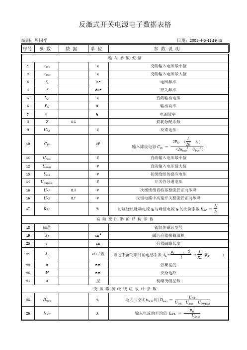
反激式开关电源电子数据表格
次级绕组匝数
NS
=
NP n
NS
=
NP
·UO+UF UOR
1
反馈级绕组匝数 NF = NS·UUFOB++UUFF12
真空中的磁导率
磁芯不留间隙时的相对磁导率μr =
AL·l µo·SJ
磁芯气隙宽度δ=
µo·SJ
Hale Waihona Puke LPP2-1 ALδ= µo NP2SJ - l
LP
µr
磁芯留间隙时的电感系数 ALG=
反激式开关电源电子数据表格
编制:周国平
日期:2005-4-5-11:19:45
序号 参 数
数 据
单 位
.
输入参数变量
参 数 说 明
1
umin
V
2
umax
V
3
fL
Hz
4
f
kHz
交流输入电压最小值 交流输入电压最大值
电网频率 开关频率
5
UO
V
6
PO
W
7
η %
反激式开关电源电子数据表格
编制:周国平 序号 参 数
27
IP
28
IR
29
IRMS
30
Lmin
31
LP
32
n
33
NP
34
NS
35
NF
36
µo
37
µr
38
δ
39
ALG
40
BM
41
DPM
42
Dpm
43 公制线径
44
SP
45
J
数 据
准谐振反激变换器

備註1
DCM(不連續電流模式)優點: 1.開關(MOSFET)為零導通損失 2.良好的輸入電壓/負載暫態變動響應 3.迴授容易達到穩定(單一極點) 4.二極體的逆向恢復時間不是很重要,因為在逆向電 壓出現前,電流就已降至零 5.可使用較小之變壓器 缺點: 1.在開關(MOSFET)和二極體會出現高的峰值電流 2.需要大的輸出電容值,約為操作在CCM時的兩倍
備註2
CCM(連續電流模式)優點: 1.開關(MOSFET)及二極體的峰值電流為操作在 DCM時的一半 2.不需很大的輸出電容 缺點: 1.會有二極體的逆向恢復損失 2.迴授不易達到穩定(兩個極點和一個右半平面的零 點)
綜合以上結論,當你的輸出為高電壓低電流時,最好 設計操作在DCM.反之,如果為高電壓高電流時,則最 好操作在CCM.
這些轉換器正日益走俏,並主要應用於消費電 子市場,但並非每位設計師都了解“準諧振” 背後的原理。
準諧振
“準諧振”通常是指將真實的硬開關轉換器與諧振 網路相結合。與常規的PWM轉換器相比,QR工作 所產生的開關損耗更小,但由於流經MOSFET的 RMS電流增大,因而導致較大的傳導損耗。然而 ,準諧振的主要優點之一在於能夠減小傳導或輻射 干擾的頻譜分量。
準諧振(Quasi-Resonant)反激式轉換器
Prepare by:Steve Huang Date:Aug-20-2008
引言
利用準方波諧振轉換器,亦稱準諧振(QR)轉換 器,可設計出電磁干擾(EMI)特徵波形較小的開 關電源。這些轉換器基於反激式架構,且QR控 制單元包含簡單的邏輯電路(無振蕩器),從而 使任何SMPS設計工程師都能輕而易舉的理解 準諧振。
正激准谐振开关电源工作原理
正激准谐振开关电源工作原理
嘿,朋友们!今天咱要来聊聊正激准谐振开关电源工作原理,这可真是个超级有趣的东西啊!
你看啊,就好比我们的生活中,电就像我们的血液一样重要,而开关电源呢,就是保证电能够顺畅流动的关键。
正激准谐振开关电源啊,它就像是一个聪明的指挥官。
想象一下,电源的输入就像是一群不守规矩的小家伙,横冲直撞的。
这时候正激准谐振开关电源就出马了!它通过一系列神奇的操作,把这些小家伙们都梳理得服服帖帖,变成我们需要的稳定电能。
正激准谐振开关电源里面有好多关键的部分呢!比如说那个变压器,就像是一个魔法盒子,把电的能量进行转换和传递。
还有那些电子元件,它们齐心协力地工作着,确保一切都有条不紊。
“哎呀,那它到底是怎么做到的呀?”你可能会这么问。
嘿嘿,它就像是一个节奏感超强的音乐家,能够精准地把握节奏,让电流和电压在合适的时候达到和谐共鸣!这可不是一般的厉害啊!
咱再举个例子,如果你家里的电器没有一个好的开关电源,那可能一会儿灯忽明忽暗,一会儿电视又出问题,多烦人呐!但有了正激准谐振开关电源,这些问题统统都不见啦!
在各种电子设备中,正激准谐振开关电源都发挥着至关重要的作用,没有它,我们的生活可就要乱套啦!它就像一个默默守护我们的小英雄,虽然我们可能平时不太会注意到它,但它一直在那里,兢兢业业地工作着。
所以说啊,正激准谐振开关电源的工作原理真的超级重要,我们真应该好好了解它,感谢它为我们的生活带来的便利呀!。
准谐振反激式电源原理(NCP1207 P38)
准谐振式开关电源的设计
摘要
随着电力电子技术的发展,电力电子设备与人们的工作、生活的关系日益密切, 而电子设备都离不开可靠的电源。开关电源产品广泛应用于工业自动化控制、特殊用 途设备、仪器仪表、半导体制冷制热等领域。 目前,开关电源以小型、轻量和高效率的特点被广泛应用于电子设备,是当今电 子信息产业不可缺少的一种电源方式。目前由于开关电源频率的提高,需要减少开关 损耗。谐振电路,以使开关上的电压或通过开关的电流呈正弦波,在减少开关损耗的 同时也可控制浪涌的发生,这种方式的开关电源称为谐振式开关电源。 准谐振开关电源使开关电源的可靠性、纹波干扰等问题得到很大改善,材料成本 不增加 而体积、重量却可以大大减少。除此之外,谐振式开关电源电路还可以克 服 PWM 方式对负载的瞬态响应较差和易辐射等缺点,利用高频驱动的作用,降低损耗, 提高效率,减少噪声。其中,部分谐振方式,将会成为主流技术。部分谐振转换电路 技术,在理论上即可实现高频化又可降低噪声,但部分谐振转换技术的实际应用仍存 在着技术问题,故仍需在这一领域开展大量的工作,以使得该项技术得以实用化。 本文叙述了准谐振式开关电源的设计过程,描述了主电路的参数计算、器件的选择, 介绍了 NCP1207 芯片实现准谐振控制的电路完整形式,实现了退磁检测、过流保护、过压 保护、电压反馈。 关键字:准谐振,开关电源,反激式,NCP1207
I
Quasi-resonant switching power supply design
Abstract
With the development of power electronics, power electronics equipment becongme more and more Important for us, electronic devices can not do without reliable power. Switching power supply products are widely used in industrial automation and control, special purpose equipment, instrumentation, semiconductor refrigeration and heat and so on. At present, switching power supply to small, light weight and high efficiency characteristics are widely used in electronic equipment, and it is not a lack of power means. At present, because of the increased frequency ,switching power supply needs to reduce switching losses. Resonant circuit, in order to switch the voltage or current through the switch was a sine wave, reduces the switching losses and also control the surge in place.This approach is called resonant switching power supply. Quasi-resonant switching power supply make problem such as switch power source reliability , lines wave interference got very big improvement,and does not increase cost and reduce the volume and weight. In addition, the resonant switching power supply can overcome the poor transient response and easy radiation defects of PWM mode to load,and use of high-frequency drivers, reducing losses, improve efficiency, reduce noise. Part of the resonant will become mainstream technology. Part of the resonant converter circuit technology, in theory, but also can reduce the noise of the high frequency, but some of the practical application of resonant conversion technology, there are still technical problems, it still required much work in this area in order to make the technology to practical use. This paper describes the quasi-resonant switching power supply design process, describe the main circuit parameter calculation, the device of choice, introduced the NCP1207 chip quasi-resonant control circuit complete the form and realized the demagnetization detection, over-current protection, over-voltage protection, voli-resonant,switching power supply, flyback, NCP1207
反激式变压器开关电源电路参数计算

反激式变压器开关电源电路参数计算
反激式变压器开关电源电路参数计算基本上与正激式变压器开关电源电路参数计算一样,主要对储能滤波电感、储能滤波电容,以及开关电源变压器的参数进行计算。
1-7-3-1.反激式变压器开关电源储能滤波电容参数的计算
前面已经详细分析,储能滤波电容进行充电时,电容两端的电压是按正弦曲线的速率变化,而储能滤波电容进行放电时,电容两端的电压是按指数曲线的速率变化,但由于电容充、放电的曲率都非常小,所以,把图1-19反激式变压器开关电源储能滤波电容两端电压的充、放电波形画成了锯齿波,这也相当于用曲率的平均值来取代曲线的曲率,如图1-26所示。
图1-26中,uo是变压器次级线圈输出波形,Up是变压器次级线圈输出电压正半周波形的峰值,Up-是变压器次级线圈输出电压负半周波形的峰值,Upa是变压器次级线圈输出电压波形的半波平均值,uc是储能滤波电容两端的电压波形,Uo是反激式变压器开关电源输出电压的平均值,i1是流过变压器初级线圈的电流,i2是流过变压器次级线圈的电流,Io是流过负载两端的平均电流。
从图1-26可以看出,反激式变压器开关电源储能滤波电容充、放电波形与图1-7反转式串联开关电源储能滤波电容充、放电波形(图1-8-b))基本相同,只是极性正好相反。
因此,图1-19反激式变压器开关电源储能滤波电容参数的计算方法与图1-7反转式串联开关电源储能滤波电容参数的计算方法完全相同。
反激式变压器开关电源储能滤波电容参数的计算,除了参考图1-7以外,还可以参考前面串联式开关电源或反转式串联开关电源中储能滤波电容参数的计算方法,同时还可以参考图1-6中储能滤波电容C的充、放电过程。
从图1-26中可以看出,反激式变压器开关电源与反转式串联开关电源中的储。