合金采样电阻
大品牌采样电阻,台产大毅品牌合金电阻
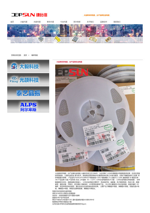
大品牌采样电阻,台产品牌合金电阻首页大毅代理光颉代理泰艺代理今台代理阿尔卑斯关于我们品牌合作联系我们大品牌采样电阻,台产品牌合金电阻大品牌采样电阻,台产品牌合金电阻 大毅科技成立於1986年,为全球第二大SMD厚膜晶片电阻制造供应商,在结合坚强的经营团队,以最先进的设 备与技术,制造高品质的零组件及最具竞争优势之价格与服务,在客户端奠定良好之信誉. 采样电阻基本参数: 产品型号 RLM12FTCMR020 电阻阻值 0.02Ω 电阻精度 1% 封装尺寸 1206 温度系数 50 额定功率1W 产品品牌 大毅 产品材质 合金 工作温度 -55~+125℃ 1206合金电阻相关尺寸图: 1206合金电阻功率曲线图: 功率随温度发生变化,温度越高功率越小。
1206合金电阻主要用于:电池保护板,适配器,电子烟控制板,电动工具,智能家居,通信设备,平衡车,定位模块 伺服电机,LED照明设备等产品。
本公司大量备货1206合金电阻,阻值1毫欧~50毫欧,欢迎来电咨询及查货,捷比信实业合金电阻优质供应商。
主要产品 厚膜晶片电阻、厚膜晶片排阻、低阻抗晶片电阻、薄膜晶片电阻、微阻抗金属电阻器、薄膜晶片保险丝。
电路中如何选择合适的电阻简析2016年云计算四大发展趋势张进华:充电桩数量不足不是最大阻碍晶振在VR产品中的应用泰艺TY系列2520封装TCXO 温补晶振频点最大可做52MHZ智能电动平衡车电路设计图台湾光颉LRP系列合金电阻温漂系数低至50ppm满足航空应用对电阻性能的新需求您现在的位置:首页 >毫欧电阻满足航空应用对电阻性能的新需求光颉0201*4贴片排阻军标级电阻 0.01%精密电阻 万分之一精度电阻 薄膜精密电阻精密电阻 合金电阻 大功率电阻 采样电阻 毫欧电阻 台湾大毅 台湾光颉 产品中心 联系方式 品牌合作 Kingbright代理 今台代理知识版权所有 Copyright © All RIGHTS RESERVED. 网站统计。
采样电阻(电流检测电阻)基本原理、安装技术与选择方法
采样电阻(电流检测电阻)基本原理、安装技术与选择方法一、电流检测电阻基本原理根据欧姆定律,当被测电流流过电阻时,电阻两端的电压与电流成正比。
当1W的电阻通过的电流为几百毫安时,这种设计是没有问题的。
然而如果电流达到10-20A,情况就完全不同,因为在电阻上损耗的功率(P=I2xR)就不容忽视了。
我们可以通过降低电阻阻值来降低功率损耗,但电阻两端的电压也会相应降低,所以基于取样分辨率的考虑,电阻的阻值也不允许太低.二、长期稳定性对于任何传感器来说,长期稳定性都非常重要.甚至在使用了一些年后,人们都希望还能维持早期的精度.这就意味着电阻材料在寿命周期内一定要抗腐蚀,并且合金成分不能改变。
要使测量元件满足这些要求,可以使用同质复合晶体组成的合金,通过退火和稳定处理的生产制程,以达到基本热力学状态。
这样的合金的稳定性可以达到ppm/年的数量级,使其能用于标准电阻。
表面贴装电阻在140℃下老化1000小时后阻值只有大约-0.2%的轻微漂移,这是由于生产过程中轻微变形而导致的晶格缺损造成的。
阻值漂移很大程度上由高温决定,因此在较低的温度下比如+100℃,这种漂移实际是检测不出来的。
三、端子连接在低阻值电阻中,端子的阻值和温度系数的影响往往是不能忽略的,实际设计中应充分考虑这些因素,可以使用附加的取样端子直接测量金属材料两端的电压。
由电子束焊接的铜-锰镍铜电阻实际上具有这样低的端子阻值,通过合理的布线可以作为两端子电阻使用而接近四端子连接的性能。
但是在设计时一定要注意取样电压的信号连线不能直接连接取样电阻的电流通道上,如果可能的话,最好能够从取样电阻下面连接到电流端子并设计成微带线。
四、低阻值四引线设计推荐用于大电流和低阻值应用。
通常的做法使用锰镍铜合金带直接冲压成电阻器,但这不是最好的办法。
尽管四引线电阻有利于改进温度特性和热电压,但总阻值有时高出实际阻值2到3倍,这会导致难以接受的功率损耗和温升。
此外,电阻材料很难通过螺丝或焊接与铜连接,也会增加接触电阻以及造成更大的损耗。
台湾天二大阻值合金采样电阻TGL系列选型规格书
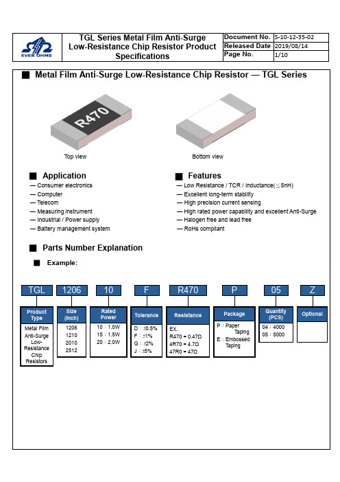
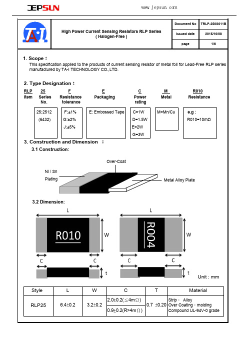
■Metal Film Anti-Surge Low-Resistance Chip Resistor — TGL SeriesTop view Bottom view■Application█Features— Consumer electronics — Low Resistance / TCR / Inductance(≦5nH)— Computer — Excellent long-term stability— Telecom — High precision current sensing— Measuring instrument — High rated power capability and excellent Anti-Surge — Industrial / Power supply — Halogen free and lead free— Battery management system — RoHs compliant■Parts Number Explanation■Example:Final Milestone DateCheckpointTGL1206F R470P05Size (Inch) 1206 1210 2010 2512ToleranceD:±0.5%F:±1%G:±2%J:±5%PackageP:PaperT apingE:EmbossedT apingQuantity(PCS)04:400005:5000ZOptionalProductTypeMetal Film Anti-SurgeLow-ResistanceChip ResistorsResistanceEX.R470=0.47Ω4R70=4.7Ω47R0=47Ω10RatedPower10:1.0W15:1.5W20:2.0W■Standard Electrical SpecificationsType RatedPowerat 70℃Max.RatedCurrentMax.OverloadCurrentT.C.R.(ppm/℃)Resistance RangeD(0.5%), F(1.0%), G(2.0%), J(5.0%)TGL1206 1W 3.16A 7.07A±50 100 mΩ ≦R ≦50 ΩTGL1210 1W 3.16A 7.07ATGL2010 1.5W 3.87A 8.66A±50 100 mΩ ≦R ≦50 ΩTGL2512 2W 4.47A 10.00A● For non-standard parts, please contact our sales dept.● Operating Temperature Range :−55℃〜+155℃.■Anti-Surge Ability:■Type Dimension■Construction Unit:mmTYPE L W H I1I2 TGL1206 3.10±0.10 1.60±0.10 0.55±0.10 0.40±0.20 0.45±0.20 TGL1210 3.10±0.10 2.50±0.15 0.55±0.10 0.50±0.20 0.50±0.20 TGL2010 5.00±0.20 2.50±0.15 0.55±0.10 0.60±0.25 0.60±0.25 TGL2512 6.30±0.20 3.20±0.20 0.55±0.10 0.65±0.25 0.65±0.25①Alumina Substrate ⑥Top Protective Overcoat②Resistive Layer ⑦Marking③Bottom Inner Electrode (Cu) ⑧Side Inner Electrode④Top Inner Electrode ⑨Barrier Layer (Ni)⑤Bottom Protective OvercoatWhite⑩Solder coating (Sn)■ Perfo r mance CharacteristicsPower Derating Curve ■The Operating Temperature Range: -55°C ~+155°C.Power rating or current rating is in the case based on continuous full-load at ambient temperature of 70℃. For operation at ambient temperature in excess of 70℃, the load should be derated in accordance with figure of derating Curve.■ Rated CurrentResistance Range: ≦ 1ΩRated Current: The resistor shall have a DC continuous working current or a AC (rms) continuous working current at commercial-line frequency and wave form corresponding to the power rating, as determined formula as following:I = Rated current (A) P= Rated Power (W) R= Resistance(Ω)■ Rated VoltageResistance Range: > 1ΩRated Voltage: The resistor shall have a DC continuous working voltage or a RMS AC continuous working voltage at commercial-line frequency and wave form corresponding to the power rating, as determined formula as following:V = Rated voltage (V)V = √P ×R P = Rated power (W)R = Nominal resistance (Ω)-5520406080100020406080100120140155℃Ambient Temperature (℃)Power Ratio(%)DERATING CURVE70160■Reliability Test and RequirementTest Item Test Method Procedure Requirements TemperatureCoefficient of Resistance(T.C.R) JIS C 5201-1clause 4.8TCR +125 ℃, 25 ℃is the reference temperatureRefer to StandardElectrical SpecificationsShort Time Overload JIS C 5201-1clause 4.135 times rated power for 5 seconds. ±(1.0%+0.001Ω)Insulation Resistance JIS C 5201-1clause 4.6100V for 1 minute. ≧10GΩDielectric Withstanding Voltage JIS-C5201-1clause 4.71206、1210、2010、2512 for 500 VAC 1minNo short or burned on theappearance.Core Body Strength JIS-C5201-1clause 4.15Central part pressurizing force:10N , 10 seconds No brokenSolderability JIS C 5201-1clause 4.17245±5°C for 3±0.5secs.>95% CoverageNo Visual damageResistance to Soldering Heat JIS-C5201-1clause 4.181. Molten solder, 260±5 °C,10±1 seconds immersion time2. IR reflow, refer to solder reflow temperature condition±(1.0%+0.001Ω)No Visual damageLeaching JIS-C5201-1clause 4.18260±5℃for 30 seconds.>95% CoverageNo Visual damageTemperature Cycling JIS C 5201-1clause 4.19-55℃to +155℃, 300 cycles±(1.0%+0.001Ω)No Visual damageLoad Life in Humidity JIS C 5201-1clause 4.2440±2℃, 90~95% R.H. , Rated power or Max. workingcurrent whichever is less for 1000 hrs with 1.5 hrs〝ON〞and 0.5 hr〝OFF〞.±(1.0%+0.001Ω)Load Life (Endurance) JIS C 5201-1clause 4.2570±2℃, Rated power, or Max. working current whichever isless for 1000 hrs with 1.5 hrs〝ON〞and 0.5 hr〝OFF〞.±(1.0%+0.001Ω)High Temperature Exposure JIS C 5201-1clause 4.25155±5℃for 1000 +48/-0 hours. ±(1.0%+0.001Ω)Resistance to Solvent JIS C 5201-1clause 4.29The tested resistor be immersed into isopropyl alcohol of20~25℃for 60 secs.Then the resistor is left in the room for 48 hrs.±(1.0%+0.001Ω)No Visual damageTerminal Strength JIS-C5201-1clause 4.32Pressurizing force for 10 seconds1206 and above:17.7NNo brokenTerminal Bending Strength JIS C 5201-1clause 4.33Bending once for 5 secondsD:1206、1210 = 3mm2010、2512 = 2mm±(1.0%+0.001Ω)No Visual damage● Temperature Coefficient of Resistance test to - 55 ℃is available on request■MarkingSolder reflow Temperature condition■Appendix For SMD Chip ResistorSIZE A ΦB ΦC■Packaging Information■Tapping SpecificationUnit: mm Packaging Type A B W E F G H T ΦD PPaper Type1206 1.90±0.2 3.05±0.28.0±0.2 1.75±0.1 3.5±0.05 4.0±0.1 2.0±0.050.75±0.1 4.0±0.11210 2.85±0.2 3.05±0.28.0±0.2 1.75±0.1 3.5±0.05 4.0±0.1 2.0±0.050.75±0.1 4.0±0.1■Embossed DimensionUnit: mm Packaging Type A B W E F G H T ΦDΦD1T1 PEmbossedType 2010 2.80±0.25.60±0.212±0.1 1.75±0.15.5±0.05 4.0±0.1 2.0±0.050.23±0.1 1.50±0.10.85±0.15 4.0±0.1 2512 3.40±0.2 6.70±0.212±0.1 1.75±0.15.5±0.05 4.0±0.1 2.0±0.050.23±0.1 1.50±0.10.85±0.15 4.0±0.1PaperCarrier■ Packing Material Data / Storage Data■ Front & Back Lead Dimension■ Top Adhesive Peel Off Strength :10~70g■ PackageInner Box Size Reel Size H(mm) 1 13 2 24 3 36 5 60 10113■ Storage Data :Storage time at the environment temp: 25±5℃& humidity: 60±20% is valid for one year from the date of delivery. External Box SizeContain (Kpcs) Length (mm)Width (mm)Width (mm)25K 180 180 60 50K 180 180 110 150K 430 200 200 300K400400200。
1206合金采样电阻 -回复
1206合金采样电阻-回复1206合金采样电阻是一种常见的电子元器件,它在电路设计和制造中起着重要的作用。
本文将从以下几个方面详细介绍1206合金采样电阻的相关知识。
一、什么是1206合金采样电阻?1206合金采样电阻是一种贴片电阻,也称为表面贴装电阻。
它采用1206封装尺寸,封装尺寸的命名方式是指器件的封装尺寸为0.12英寸长、0.06英寸宽。
1206合金采样电阻的使用广泛,可以应用于各种电子设备和电路中。
二、1206合金采样电阻的结构和特点是什么?1206合金采样电阻的结构相对简单,它主要由一条或多条金属电阻体组成,两端焊有金属引脚,以便能够与电路板上的焊盘连接。
1206合金采样电阻的特点包括以下几个方面:1. 封装小巧:1206封装尺寸的电阻相对较小,适合在空间有限的电子设备中应用。
2. 贴片结构:1206合金采样电阻采用贴片结构,使得它可以方便地焊接在电路板上,节省了安装的时间和人力成本。
3. 稳定性好:1206合金采样电阻的稳定性较高,能够提供精确的电阻值,并且能够在较宽的温度范围内保持稳定。
4. 工作电压范围广:1206合金采样电阻能够在较宽的电压范围内工作,适用于不同电路和设备的需求。
5. 耐高温性能好:1206合金采样电阻能够在一定的温度范围内工作,具有良好的耐高温性能,可以在高温环境下使用。
三、1206合金采样电阻的应用领域有哪些?由于1206合金采样电阻的特点和性能优势,它在各种电子设备和电路中都有广泛的应用。
以下是一些常见的应用领域:1. 通信设备:1206合金采样电阻可以用于手机、无线通信设备等电子产品中,起到电路保护和电阻匹配的作用。
2. 汽车电子:1206合金采样电阻可以应用于汽车电子中,如车载导航、空调控制等,帮助实现电子设备的正常工作。
3. 智能家居:1206合金采样电阻在智能家居产品中也有一定的应用,如智能插座、智能灯具等,帮助实现电路的精确控制。
4. 数字设备:1206合金采样电阻可以用于各类数字设备,如计算机、平板电脑等,辅助完成电路的功能。
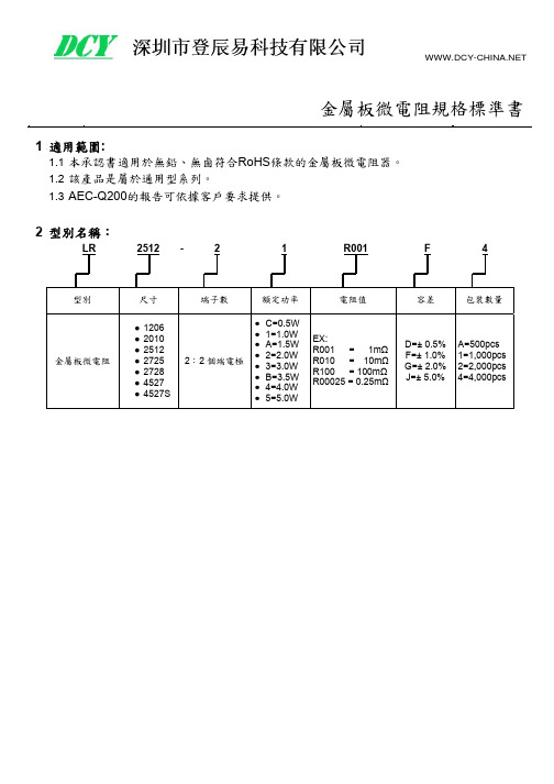
合金电阻参数对照表_顺海科技
合金电阻又被称为电流检测电阻,采样电阻,毫欧电阻等等,这个是根据合金电阻的特性所决定的。
首先,合金的电阻具有高功率,低阻值,高精度,高可靠性等特点,主要应用于电流检测电路中,因此就有了以上的别称。
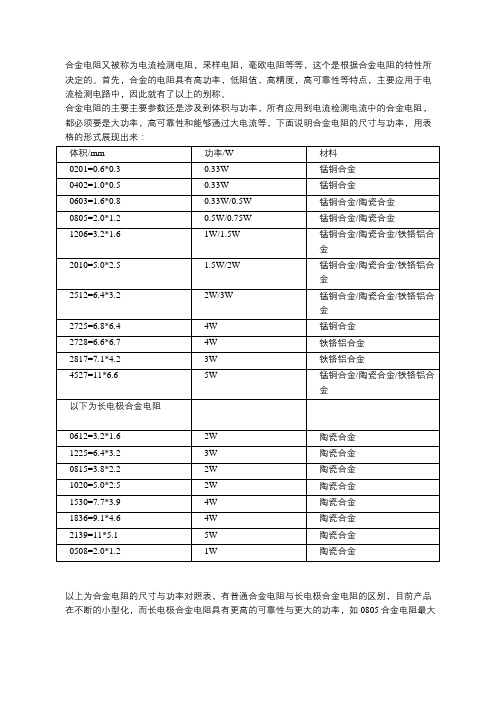
合金电阻的主要主要参数还是涉及到体积与功率,所有应用到电流检测电流中的合金电阻,都必须要是大功率,高可靠性和能够通过大电流等,下面说明合金电阻的尺寸与功率,用表格的形式展现出来:
以上为合金电阻的尺寸与功率对照表,有普通合金电阻与长电极合金电阻的区别,目前产品在不断的小型化,而长电极合金电阻具有更高的可靠性与更大的功率,如0805合金电阻最大
只能做到0.75W,而长电极0508则可以做到1W与1.2W等,更加适合小型化便携式产品。
更多产品参数欢迎咨询相关销售。
合金电阻的各大规格参数
合金电阻的各大规格参数电阻使电路当中使用中最多的一种电子元器件,一块电路板上面基本上出现的电阻随处可见,在不同电路有着不一样的作用,有限流作用,有分压作用,有作为负载用。
而合金电阻是电阻里面较为特殊的一种,那么什么是合金电阻,合金电阻又有哪些作用呢?合金电阻主要是用来检测电流的,因为又称为:采样电阻,电流检测电阻等。
合金电阻的主要特征有:1.超低阻值(0.2mR~680mR)2.高功率(0.5W~15W)3.超低电感量(趋0,也是无感电阻的一种)4.尺寸有(0402,,0603,0805,1206,1210,2010,2512,2725,2728,4527,5927等)5.合金电阻的材料种类有(纯合金,锰铜合金,陶瓷合金等)6.合金电阻的常规品牌有(Vishay,SUSUMU,ELLON,Viking,RALCE,YAGEO,EVER OHMS,华德,ROHM等)7.合金电阻的焊点主要有宽边电极,短边电极,四脚焊锡等合金电阻的应用领域:合金电阻的应用几乎涵盖了所以跟电池有关的所以产品,如电池保护板,小家电,伺服电机,变频器,电源适配器,电源,PLC等等具体的选型还是看功率和温漂或阻值来定,目前在温度系数和功率要求不高的3C产品,很多会用普通的低阻电阻节省成本,满足产品利润最大化,有的也会用厚膜高功率的超低阻值满足检测需求,节省成本。
目前合金电阻的单价较普通低阻来说价格贵,交期长且单机用量不大,导致采购成本较高。
深圳市顺海科技有限公司代理经销台湾天二(EVER OHMS),亿能(ELLON),华德,旺诠(RALEC),光颉(Viking),威世(Vishay),SUSUMU,国巨(YAGEO)等品牌的合金电阻,超低阻值电阻,车规电阻,另外公司还有贴片电容,功率电感,贴片保险丝,连接器等产品。
公司仓储雄厚,价格优势,原厂直供,以最大限度的控制成本以及采购时间,一站式服务。
Resistor.Today-KWSL系列四脚开尔文合金采样电阻规格书

焊脚温度( ℃)
额定功率 (%)
0
0
Q
9
系列号 KWSL
精度 F=±1% G=±2% J=±5%
阻值
L300=0.3mΩ L500=0.5mΩ 1L00=1mΩ 2L00=2mΩ 3L00=3mΩ
KWSLF1L00Q9 5W 1mΩ ±50ppm 6.6±0.3 6.9±0.3 3.0±0.3 4.8 0.9 2.5 0.33
KWSLF2L00M9 5W 2mΩ ±20ppm 6.6±0.3 6.9±0.3 3.0±0.3 4.8 0.9 2.5 0.50
KWSLF3L00M9 4W 3mΩ ±20ppm 6.6±0.3 6.9±0.3 3.0±0.3 4.8 0.9 2.5 0.34
温飘 M=±20ppm Q=±50ppm
包装 9=标准品
85℃ ,85% RH ,10% 额定功,率 1000 h 100 g 6 ms ,5 个脉冲
10 Hz to 200 Hz 1分钟,频率变化 , 3 个方向, 12h 1000h at+70℃,1.5h开,0.5h关,额定功率 + 260℃锡槽,保持10s
参数
± (1.0%+0.0005Ω)ΔR ± (0.5%+0.0005Ω)ΔR ± (0.5%+0.0005Ω)ΔR ± (1.0%+0.0005Ω)ΔR ± (0.5%+0.0005Ω)ΔR ± (0.5%+0.0005Ω)ΔR ± (0.5%+0.0005Ω)ΔR ± (1.0%+0.0005Ω)ΔR ± (0.5%+0.0005Ω)ΔR
2010合金采样电阻常用型号查询表
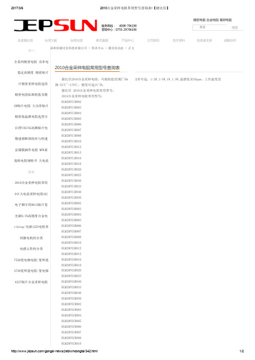
深圳市捷比信科技有限公司 > 资讯中心 > 捷比信动态 > 正文捷比信2010合金采样电阻,可做阻值范围2~50mR,功率可选,1/2W,3/4W,1W,1.5W,温漂低至50ppm。
工作温度范围-55℃~+170℃,精度可选1%~5%.捷比信 2010合金采样电阻常用型号:2010合金采样电阻常用型号:RLM20FEIR002RLM20FEIR003RLM20FEIR004RLM20FEIR005RLM20FEIR006RLM20FEIR007RLM20FEIR008RLM20FEIR010RLM20FEIR012RLM20FEIR015RLM20FEIR016RLM20FEIR018RLM20FEIR020RLM20FEIR025RLM20FEIR030RLM20FEIR033RLM20FEIR040RLM20FEIR050RLM20FESR002RLM20FESR003RLM20FESR004RLM20FESR005RLM20FESR006RLM20FESR007RLM20FESR008RLM20FESR010RLM20FESR012RLM20FESR015RLM20FESR016RLM20FESR018RLM20FESR020RLM20FESR025RLM20FESR030RLM20FESR033RLM20FESR040RLM20FESR050RLM20FECR002RLM20FECR003RLM20FECR004RLM20FECR005RLM20FECR006RLM20FECR007RLM20FECR008RLM20FECR010热门全系列精密电阻 功率电高稳定高精度 精密贴片贴片精密采样电阻选用精密电阻标准阻值及精2W贴片电阻 大功率贴片精密低温漂电阻选型方台湾VIKING高频贴片电慢速熔断保险丝与快速金属膜插件电阻 MFR系毫欧电阻规格书 大电流最新2010合金采样电阻常用0Ω大电流采样电阻LRJ 电子烟专用0612贴片宽光颉0.5%高精度合金电viking/光颉1225电阻常伺服电机的分类电感元件的分类7520宽电极电阻/宽焊盘3720宽焊盘电阻/宽电极4527贴片合金采样电阻2010合金采样电阻常用型号查询表精密电阻 合金电阻 毫欧电阻搜索搜索走进捷比信台湾大毅台湾光颉泰艺晶振产品中心公司资讯技术资料投资者关系战略合作RLM20FECR012RLM20FECR015RLM20FECR016RLM20FECR020RLM20FECR025RLM20FECR030RLM20FECR040RLM20FECR050RLM20FEDR002RLM20FEDR003RLM20FEDR004RLM20FEDR005RLM20FEDR006RLM20FEDR007RLM20FEDR008RLM20FEDR010RLM20FEDR012RLM20FEDR015RLM20FEDR016RLM20FEDR018RLM20FEDR020RLM20FEDR025RLM20FEDR030RLM20FEDR033RLM20FEDR040RLM20FEDR050..查货,索样请来电洽询深圳市捷比信科技有限公司。
合金贴片电阻
合金贴片电阻
合金贴片电阻又称为电流检测电阻,电流感测电阻,合金取样电阻,电流感应电阻,合金电阻。
材料介绍
英文一般译为Sampling resistor,Current sensing resistor。
电阻主要材料为铜,再加上其他的材料就成了康铜,锰铜等。
其他辅助材料众多,但主要性能由合金材料本身决定。
通俗的讲合金贴片电阻就是一个贴片采样电阻阻值较小的电阻,串联在电路中用于把电流转换为电压信号进行测量。
合金贴片电阻采用符合高功率电气特性、高纯度、高导热、低温漂及耐高温的特殊合金,一体成型无切割的结构,大幅降低电路板上的散热面积,可达到几乎无电感值。
合金电阻作为电流载体,阻值精准,温度稳定性,产品的安全性,稳定性明显高于普通的陶瓷电阻。
同时金属的导热性也是它同其他电阻一大优势。
特别是在电源以及其它相关产品的应用中,瞬间的冲击电流,短路电流或脉冲电流产生时,合金当做首选作为电流介质来检测电流。
合金采样电阻的作用
合金采样电阻的作用采样电阻分类两种,一种是电流采样电阻,另一种是电压采样电阻,我们在电流设计的时候所说的采样电阻,一般是电流采样电阻。
采样电阻在工程实际电流的应用中有不同的说法,一般通俗的说法都是电流采样电阻,电流检测电阻,电流取样电阻,由于其材质的特殊性,一种为普通厚膜低阻值电阻,在要求不高的消费类产品上也可以起到电流检测的作用,但是在工业控制以及高要求的电池保护系统时,则必须使用合金材质的电阻进行电流采集,所以也被称为合金电阻或者合金采样电阻。
合金采样电阻的主要特点有如下几点:1、材质为合金,主要材质为铜,加上其他材质后形成锰铜,康铜,镍铜等等。
2、低阻值,阻值低可以做到0.2mR~4R(根据尺寸来确定),一般以25728为主,但是随着现在便携式产品的不断小型化和低功耗等要求,合金采样电阻也在逐渐小型化,如0805,0603,0402等。
3、高功率,功率都比普通电阻和升功率电阻的要高,如:1206普通电阻的功率为1/4W,1206升功率电阻的功率为1/2W,1206合金电阻的功率为1W/1.5W。
4、低温度系数,TCR值ppm/℃。
温度系数有25ppm,50ppm,75ppm,100ppm。
普通低阻值电阻的温度系数为100ppm/200ppm.5、高精度,一般普通低阻值电阻为5%,1%,而合金采样电阻为1%,0.5%。
6、抗大电流冲击,由于其特殊合金材质,具有更好的耐大电流冲击特性,加上功率越高,电流越大的特性。
合金采样电阻,是按照产品使用的功能来划分电阻。
合金采样电阻一般取样的对象是电流信号或者电压信号,采样电阻的精度一般都会控制在1%或者1%以下,功能上就是做为参考,常用在反馈电路中,以稳压电源电路为例,为使输出的电压保持恒定状态,要从输出电压取一部分电压做参考(常用取样电阻的形式),如果输出高了,输入端就自动降低电压,使输出减少;若输出低了,则输入端就自动升高电压,使输出升高。
一般使用在电源产品,或者电子,数码,机电产品的电源部分,功能强大。
大毅锰铜合金采样电阻RLP25_MnCu系列选型手册
170℃, 1000hrs -55℃, 1000hrs Bending width 2mm 100V DC for 1 minute
Note:2&3watts total Solder pad and trace size of 300mm
深圳捷比信--高品质精密元件供应商
www.jepsun.com
QTY: 4000 PCS
LOT NO:
MR010 FEE
RLP25FEEM
T019C0071H
0308
Tolerance
Package
Power Rating
9. Taping
Packing
Emboss
Type RLP25
A
3.6±0.2
B
6.9±0.2
W
12.±0.2
F
5.5±0.05
E
1.75±0.1
Iron Solder:350±10℃ , 3+1/-0 sec
Peak : 260
5
℃ , 5 sec
15. ECN
Engineering Change Notice: The customer will be informed with ECN if there is significant modification on the characteristics and materials described in approval sheet.
Issued date page
10. Reel Specification
Series RLP 25
ψA
+0
ψB 60 ±1.0
-3
ψC 13.0±1.0
LR2512全系列合金采样电阻原厂推荐
0.3mΩ: ≦±450 0.5~0.9mΩ: ≦±175
1.0mΩ: ≦±75 0.5~0.9 mΩ: ≦±100 1.0~1.9mΩ: ≦±75 2.0~4.0mΩ: ≦±50 3.1~6.9mΩ: ≦±25 7.0~100mΩ: ≦±15
3.0
0.6 ~ 3.0 4.0 ~ 5.0
0.450±0.010 0.270±0.010 (11.430±0.254) (6.850±0.254)
0.055±0.010 (1.400±0.254)
0.127±0.010 (3.215±0.254)
5.1 ~ 20
0.071±0.010 (1.815±0.254)
0.031±0.010 (0.787±0.254) 0.0254±0.010 (0.645±0.254) 0.040±0.010 (1.000±0.254)
0.031±0.010 (0.787±0.254)
0.025±0.010 (0.645±0.254)
0.039±0.010 (0.991±0.254)
4.1 ~75.0
0.246±0.010 0.126±0.010 0.025±0.010 0.044±0.010 (6.248±0.254) (3.202±0.254) (0.645±0.254) (1.118±0.254)
75.1 ~ 100.0
0.025±0.010 0.034±0.010 (0.645±0.254) (0.868±0.254)
3.2 額定電流:
合金采样电阻过载倍数曲线
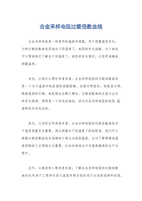
合金采样电阻过载倍数曲线
合金采样电阻是一种常用的温度传感器,用于测量温度变化。
它的过载倍数曲线是指在不同温度下,电阻的变化倍数。
这个曲线
可以帮助我们了解在不同温度下,电阻的变化情况,从而更准确地
测量温度。
首先,让我们从理论角度来看。
合金采样电阻的过载倍数曲线
是一个关于温度和电阻值的函数图像。
在绝对零度时,电阻值为零,随着温度的升高,电阻值也会随之增加。
过载倍数曲线会显示出这
种变化规律,通常是一个非线性曲线,因为合金采样电阻的电阻-温
度特性并非线性的。
其次,从实际应用角度来看。
合金采样电阻的过载倍数曲线对
于温度测量至关重要。
通过测量在不同温度下的电阻值,我们可以
根据过载倍数曲线来准确地计算出当前的温度。
这对于需要精准温
度控制的工业领域尤为重要,比如在制造业中对温度敏感的生产过
程中。
此外,从制造和工程角度来看。
了解合金采样电阻的过载倍数
曲线也有助于工程师在设计温度传感系统时进行合适的选择和安排。
他们可以根据过载倍数曲线来确定合金采样电阻的最佳工作范围,以及在不同温度下系统的响应情况。
最后,从数据分析角度来看。
合金采样电阻的过载倍数曲线也可以用于数据分析和预测。
通过对历史数据和过载倍数曲线的对比分析,可以发现温度变化的规律,从而预测未来的温度变化趋势。
总的来说,合金采样电阻的过载倍数曲线对于理论研究、实际应用、制造工程和数据分析都具有重要意义。
它是温度传感器设计和使用中不可或缺的重要参考依据。
希望以上回答能够全面地解答你的问题。
合金电阻电流采样电路

合金电阻电流采样电路
在电流采样电路中,合金电阻通常被放置在电路中,以便测量
电流。
当电流通过合金电阻时,合金电阻的温度会上升,从而改变
其电阻值。
通过测量合金电阻的电阻值变化,可以推导出电流的大小。
合金电阻电流采样电路通常包括合金电阻本身、电流输入端和
电压输出端。
当电流通过合金电阻时,产生的电压信号可以通过放
大电路进行放大,然后通过模数转换器转换为数字信号,从而实现
对电流的精确测量。
在设计合金电阻电流采样电路时,需要考虑合金电阻的特性、
电压放大器的设计、模数转换器的选择以及输出数字信号的处理等
方面。
此外,还需要考虑电路的稳定性、精度和抗干扰能力等因素。
总的来说,合金电阻电流采样电路在工业控制、电力电子和仪
器仪表等领域有着广泛的应用,它能够准确地测量电路中的电流,
并且具有较高的稳定性和精度。
5mω合金电阻
5mω合金电阻
5mΩ(毫欧)合金电阻是一种低阻值、高精度的电阻器,主要用于电流检测或采样应用场合,比如电池管理系统(BMS)、电源电路中的电流监控、电子负载测试设备等。
这类电阻通常具有非常小的阻值,能够以极低的电压降精确反映通过的大电流,同时要求其在工作状态下产生的热量要尽可能少地影响电阻值的稳定性。
设计上,为了有效地处理大电流和快速散热,5mΩ合金电阻通常采用特殊的合金材料制成,这些材料具有较低的温度系数和较高的热稳定性。
此外,它们可能会被封装在SMD (表面贴装器件)形式中,例如0805、1206、2512等尺寸,以便于电路板上的安装,并且可能配备有良好的散热结构,如金属底座或者直接采用导热性好的基材进行封装,从而降低热内阻,提高整体性能及可靠性。
由于此类电阻需承载较大的功率,因此在选择时需要考虑其额定功率、长期稳定性、温漂系数以及工作环境下的耐温等级等因素。
测量该合金的电阻率设计的实验

测量该合金的电阻率设计的实验
测量合金的电阻率可以采用四线法测量。
实验步骤如下:
1. 首先准备一个合金样品,并将其切割成一个适合的形状,如长条或片状。
2. 使用细砂纸或砂轮将合金样品的两侧表面打磨光滑,以去除表面的污垢和氧化层。
3. 使用电阻计测量合金样品的直流电阻。
(记作R1)
4. 使用铜线或铝线连接一个恒流电源和一个毫伏计。
5. 将合金样品夹持在两个金属电极之间,确保好接触。
6. 开启恒流电源,并测量在通过合金样品时的电压降。
(记作V1)
7. 计算通过合金样品的电流值(I),使用欧姆定律:I = V1 / R1。
8. 将合金样品的长度测量,并记录下来。
9. 将合金样品的横截面积测量,并记录下来。
10. 计算合金样品的电阻率(ρ):ρ = R1 * (A / L),其中A为
横截面积,L为长度。
重复以上步骤多次进行测量,取多个数据的平均值,以提高实验结果的准确性。
注意事项:
- 确保合金样品的两侧表面完全平行,以确保电阻测量的准确性。
- 使用四线法测量可以减小连接线的电阻对实验结果的影响。
- 考虑合金样品所处的温度,可以进行温度修正以得到更准确的电阻率值。
- 确保恒流电源的稳定性,以保证电流的恒定。
- 在进行电阻测量和电流测量时要小心防止触电和短路。
合金采样电阻
合金采样电阻
合金采样电阻是一种用于测量电阻和电导率的电子器件,广泛应用于材料科学、电子工程、半导体工业等领域。
它是由一段合金线制成的,通过将电流传送到这条合金线上,来测量电阻和电导率的变化。
合金采样电阻最常用的是四探针测量法,它可以提供精确的电阻和电导率测量结果,对于具有高精度要求的应用尤为重要。
四探针测量法的原理是通过四个细探针在测试样品上形成一个矩形电路,然后将电流传递到其中两个探针,通过另外两个探针测量样品两个端点之间的电压差,从而计算出样品的电阻和电导率。
合金采样电阻的应用很多,例如在材料科学领域,它可以用于测量金属、半导体和绝缘体的电阻和电导率,帮助科学家研究材料的热电性质和超导行为。
在电子工程领域,合金采样电阻可以用于测量电路中的电阻、电流和电压,判断电路的可靠性和稳定性。
在半导体工业中,合金采样电阻可以用于控制半导体器件的制造过程,确保器件的性能和质量。
不同的合金采样电阻具有不同的特性,例如,金属合金采样电阻由于具有良好的热导率和电导率,适用于高温环境和高频应用。
另外,金属合金采样电阻还可以被制成非线性元件,用于电流保护和电压调节。
而半导体合金采样电阻则具有更高的灵敏度和更低的温度系数,适用于需要高精度测量的应用场合。
总之,合金采样电阻是一种非常重要的电子器件,它可以帮助科学家和工程师测量物质的电阻和电导率等物理性质,为材料科学、电子工程和半导体工业等领域的发展做出更大的贡献。
合金电阻的详细分类
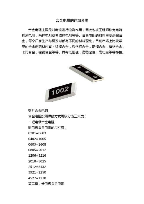
合金电阻的详细分类
合金电阻主要是对电流进行检测作用,因此也被工程师称为电流检测电阻,采样电阻或者取样电阻等等。
合金电阻的材料主要是铜合金,每个厂家生产与研发时都有不同的材料配比,目前市场上比较常见的合金电阻材料有:锰铜合金,铁铬铝合金,康铜合金,镍铬合金,卡玛合金,镍铜合金等等。
具有低阻值,高稳定性,高功率等等特性。
贴片合金电阻
合金电阻按照焊线方式可以分为三大类:
:短电极合金电阻
短电极合金电阻的尺寸有:
0201=0603
0402=1005
0603=1608
0805=2012
1206=3216
2010=5025
2512=6432
3921=1250
4527=1270
第二类:长电极合金电阻
0603=0306
0805=0508
1206=0612
2512=1225
3921=2139
第三类:四脚合金电阻
1206
2512
合金电阻根据根据材料可以分为几大类:
一:锰铜合金,这一类产品稳定性比较高,主要集中在0.004R以下的阻值。
稳定性好。
二:铁铬铝合金,铁铬铝合金主要是集中在0.004R及以上的阻值。
稳定性好。
三:康铜合金,常规合金阻值都可以。
四:镍铜合金,常规合金阻值都可以。
五:镍铬合金,常规合金阻值都可以。
六:卡玛合金,常规合金阻值都可以,这种材料成本高,因此生产的厂商很少。
七:陶瓷合金,0.001R以下的尺寸无法生产,但是可以做高阻值,知道0.75R都可以,具体体积对应阻值会不一样。
- 1、下载文档前请自行甄别文档内容的完整性,平台不提供额外的编辑、内容补充、找答案等附加服务。
- 2、"仅部分预览"的文档,不可在线预览部分如存在完整性等问题,可反馈申请退款(可完整预览的文档不适用该条件!)。
- 3、如文档侵犯您的权益,请联系客服反馈,我们会尽快为您处理(人工客服工作时间:9:00-18:30)。
Metal Alloy 6PDOO-Resistance Resistor
Product Specifica tion: 6R2512 3W Type
FEATURESΚ
Ideal for all types of current sensing, voltage division and
Pulse applications including switching and linear power
Supplies, Instruments, power amplifiers.
Proprietary processing technique produces extremely low
Resistance values.
High-temperature performance (up to +275к)
Very low inductance 0.5nH to 5nH
Excellent frequency response
Low thermal EMF (<1uV/к)
Lead(Pb)-free construction is RoHS-compliant
1. Standard Electrical SpecificationsΚ
Power Rating at 100 кResistance Range mȍ
Model
(Watts) 0.5%(D) 1.0%(F) 5.0%(J) S R2512-23 3.0 7~10 0.5~10 0.5~10
3 Watts with total solder pad trace size of 400mm²
2. Technica l Specifica tionsΚ
Parameter Unit S R2512-23
(mȍ)
Temperature Coefficient ppm /к0.5~2= +50 3~10 = -25
Operating Temperature
Range
к–65 ~ +275 Maximum Working Voltage V (P × R)½
Ordering InformationΚʳʳʳʳʳʳʳʳʳʳʳʳʳʳʳʳʳʳʳʳʳʳʳʳʳʳʳʳʳʳʳʳʳʳʳʳʳʳʳʳʳʳʳʳʳʳʳʳʳʳʳʳʳʳʳʳʳʳʳʳʳʳʳʳʳʳʳʳʳʳʳʳʳʳʳʳʳʳʳʳʳʳʳʳʳʳʳʳʳʳʳʳʳʳʳʳʳʳʳʳʳʳʳʳʳʳʳʳʳʳʳʳʳ6R2512 - 2 5 )
Packing
1=Tape & ReelΙB=Bulk Pack
1=1,000 Pcs
Tolera nce
D=±0.5%ΙF=±1.0%ΙJ=±5.0%
Resistance
EXΚR001=1mȍΙR010=10mȍ
Power RatingΰWattsα
Number of Terminals
ModelΰSizeα
3. DimensionsΚ
DIMENSIONS - in inches (millimeters)
Model Resistance
Range mȍ
L W H T
0.5 ~ 1.5 0.246±0.010
(6.25±0.254)
0.13±0.010
(3.30±0.254)
0.031±0.010
(0.80±0.254)
0.074±0.010
(1.88±0.254)
6R2512-23
2~ 10
0.246±0.010
(6.25±0.254)
0.13±0.010
(3.30±0.254)
0.031±0.010
(0.80±0.254)
0.044±0.010
(1.13±0.254) SOLDER PAD DIMENSIONS - in inches (millimeters)
Model
Resistance Range mȍ a b i
0.5 ~1.5 0.120(3.05) 0.145(3.68) 0.050(1.27) 6R2512-23
2 ~ 10 0.083(2.11) 0.145(3.68) 0.125(3.18) Remark :
3 Watts with total solder pad trace size of 400mm²
4. Power Derating CurveΚ
5. PerformanceǺ
Test Item Conditions of test Test Method Test Limits Short Time Overload 3W 3x rated power for 5 seconds JIS C5202 5.5 ²(0.5%+0.0006͈*ɆS
Resistance to Solder
Heat Solder temp./immersion time:260±5ʚ,10±1secs and
350±10ʚ,3.5±0.5secs
JIS C5202 6.4 ²(0.5%+0.0006͈*ɆS
Solderability test Steam aging:4 hrs, cool down 30 minutes then test JIS C5202 6.5 95% coverage
Vibration Frequency varied 55Hz in one minute , 3 directions , 12
hours
JIS C5202 6.7 ²(0.5%+0.0006͈*ɆS
Resistance to
solvent
Immersion time:60±5 secs,20ʚɴ25 ʚJIS C5202 6.9 ²(0.5%+0.0006͈*ɆS Mechanical Shock 100 grams for 6 milliseconds, 5 pulses JIS C5202 6.13 ²(0.5%+0.0006͈*ɆS Low Temperature
Storage
-55ʚfor 1000 hours JIS C5202 7.1 ²(0.5%+0.0006͈*ɆS High Temperature
Exposure
1000 hours @ + 155ʚJIS C5202 7.2 ²(1.0%+0.0006͈*ɆS
Thermal Shock - 55 ʚ to + 125 ʚ, 1000 cycles , 15 minutes at each
extreme
JIS C5202 7.4 ²(0.5%+0.0006͈*ɆS
Moisture Resistance Mil-STD-202 , Method 106 , 0% power , 7a and 7b not
required
JIS C5202 7.6 ²(0.5%+0.0006͈*ɆS
Bias Humidity + 85ʚ, 85% RH, 10% Bias, 1000 hours,90 minutes
"ON",30 minutes “OFF"
JIS C5202 7.9 ²(0.5%+0.0006͈*ɆS
Load Life 1000 hours @ rated power, + 100ʚ , 1.5 hours "ON" ,
0.5 hours "OFF"
JIS C5202 7.10 ²(1.0%+0.0006͈*ɆS
6. Marking Κ
002
Resistance 0.002ȍ
7. Packaging Κ
Reel
Model
Tape Width
Diameter
Pieces/Reel
Code
6R2512-23 12mm/Embossed
Plastic
178mm/7” 1,000
1
Unit: mm
Item W
P1
E
F
Do
D1
P0
Po*10
P2
Ao
Bo
Ko
t
Spec.
12.00 8.00 1.75 5.50 1.50 1.50 4.00 40.00 2.00 3.90 6.74 1.08 0.24
Tole. ±0.10 ±0.10 ±0.10 ±0.05
Џ0.10А0.00
±0.10±0.05±0.10±0.05±0.10 ±0.10 ±0.05±0.05。