CDM625内容介绍
Comtech EF Data CDM-625 Advanced Satellite Modem (

IMPORTANT NOTE: The information contained in this document supersedes all previously published information regarding this product. Product specifications are subject to change without prior notice. CDM-625Advanced Satellite Modem (18 kbps – 25 Mbps) Installation and Operation Manual For Firmware Version 2.3.1 or higherErrata A for MN-CDM625 Rev 15Comtech EF Data Documentation UpdateSubject: Change page 1-8, IP Packet Processor AES Encryption Installation Method to Available as EN model.Errata Part Number: ER-CDM625-EA15 (Errata documents are not revised)PLM CO Number: C-0035152Comments: See attached page(s). The new information will be included in the next releasedrevision of the manual.CDM-625 Advanced Satellite Modem (18 kbps – 25 Mbps)Installation and Operation ManualFor Firmware Version 2.3.1 or higherPart Number MN-CDM625Revision 15BLANK PAGETABLE OF CONTENTS TABLE OF CONTENTS (III)TABLES ................................................................................................................................ X XII FIGURES .............................................................................................................................. X XIII PREFACE (XXVII)About this Manual (xxvii)Conventions and References (xxvii)Patents and Trademarks (xxvii)Warnings, Cautions, and Notes (xxvii)Recommended Standard Designations (xxviii)Safety and Compliance ................................................................................................................. x xviii Electrical Safety and Compliance . (xxviii)Grounding (xxviii)Electrical Installation (xxix)Battery (xxix)Fuses (xxix)Operating Environment ............................................................................................................................................... x xx European Union Radio Equipment and Telecommunications Terminal Equipment (R&TTE) Directive (1999/5/EC) and EN 301 489-1 ................................................................................................................................... x xx European Union Electromagnetic Compatibility (EMC) Directive (2004/108/EC) ........................................... x xx European Union Low Voltage Directive (LVD) (2006/95/EC) ............................................................................ x xxi European Union RoHS Directive (2002/95/EC) (xxxi)European Union Telecommunications Terminal Equipment Directive (91/263/EEC) ................................... x xxi CE Mark . (xxxi)Product Support (xxxii)Comtech EF Data Headquarters (xxxii)Warranty Policy (xxxii)Limitations of Warranty (xxxiii)Exclusive Remedies (xxxiii)CHAPTER 1.INTRODUCTION ............................................................................................ 1–1 1.1Overview ............................................................................................................................ 1–1 1.2Functional Description ........................................................................................................ 1–21.3Features ............................................................................................................................. 1–3 1.3.1 Physical Description .................................................................................................................................. 1–3 1.3.2 Modem Compatibility .............................................................................................................................. 1–3 1.3.3 Verification ................................................................................................................................................. 1–4 1.3.4 Updating Modem Firmware .................................................................................................................... 1–4 1.3.5 Standard Data Interfaces ......................................................................................................................... 1–4 1.3.6 Optional Hardware and Accessories ....................................................................................................... 1–5 1.3.7 Fully Accessible System Topology (FAST) ............................................................................................... 1–6 1.3.8 Supporting Hardware and Software ....................................................................................................... 1–9 1.3.9 Physical Features ..................................................................................................................................... 1–101.3.9.1 Dimensional Envelope ....................................................................................................................... 1–101.3.9.2 Front Panel .......................................................................................................................................... 1–111.3.9.3 Rear Panel ........................................................................................................................................... 1–12 1.4Summary of Specifications ................................................................................................ 1–13 1.4.1 Modulator ................................................................................................................................................ 1–13 1.4.2 Demodulator ........................................................................................................................................... 1–15 1.4.3 Data Interfaces ........................................................................................................................................ 1–19 1.4.4 Automatic Uplink Power Control (AUPC) ............................................................................................. 1–19 1.4.5 DoubleTalk® Carrier- in-Carrier® (CnC) ................................................................................................... 1–20 1.4.6 Framing Summary ................................................................................................................................... 1–21 1.4.7 Data Rate Ranges .................................................................................................................................... 1–22 1.4.8 VersaFEC Adaptive Coding and Modulation (ACM) ............................................................................ 1–26 1.4.9 Miscellaneous .......................................................................................................................................... 1–27 1.4.10 Approvals ................................................................................................................................................. 1–27CHAPTER 2.INSTALLATION ............................................................................................. 2–1 2.1Unpack and Inspect the Shipment ....................................................................................... 2–1 2.2Install the Unit Into a Rack Enclosure ................................................................................... 2–2 2.2.1 Install the Optional Rear-Mounting Support Brackets Kits .................................................................. 2–4 2.3Configure the CDM-625 ....................................................................................................... 2–5 2.4Verify Modem Operation .................................................................................................... 2–5 2.5Connect the External Cables ................................................................................................ 2–5 CHAPTER 3.REAR PANEL CONNECTORS AND PINOUTS ............................................ 3–1 3.1CDM-625 Rear Panel Overview ............................................................................................ 3–1 3.2CDM-625 Cable Connections ............................................................................................... 3–2 3.2.1 IF Connection Group ................................................................................................................................. 3–33.2.1.1 Rx IF Connectors ................................................................................................................................... 3–33.2.1.2 Tx IF Connectors ................................................................................................................................... 3–3 3.2.2 Terrestrial Data Connection Group ......................................................................................................... 3–43.2.2.1.1 HSSI Operation via the CIC-60 Interface Adapter Module.......................................... 3–53.2.2.2 G.703 Connectors ................................................................................................................................. 3–73.2.2.2.1 Balanced G.703 (DB-9F) .............................................................................................. 3–73.2.2.2.2 Aux G.703 (DB-9F) ....................................................................................................... 3–73.2.2.2.3 Quad E1 Operation via the Balanced G.703 / Aux G.703 Connectors ........................ 3–83.2.2.2.3.1 CA-0000163 Adapter Cable .................................................................................. 3–83.2.2.2.3.2 CA-0000164 Adapter Cable .................................................................................. 3–93.2.2.2.3.3 KT-0000122/KT-0020570 Quad E1 Balanced/Unbalanced Adapter Cable Kits . 3–103.2.2.2.4 Unbal G.703 / ASI – Out (IDO), In (DDI) .................................................................... 3–113.2.2.2.5 G.703 IDI (Insert Data In), DDO (Drop Data Out) ...................................................... 3–113.2.2.3 Quad 10/100 Ethernet (RJ-45) .......................................................................................................... 3–113.2.2.4 IDR Data / Alarms / Audio (HD-44F) ................................................................................................. 3–113.2.2.5 ESC (DB-9F) .......................................................................................................................................... 3–12 3.2.3 Utility Connections Group ...................................................................................................................... 3–123.2.3.1 Remote Control (DB-9M) .................................................................................................................. 3–123.2.3.2 Alarms (DB-15M) ................................................................................................................................ 3–133.2.3.3 PMSI Connector, DB-9F ..................................................................................................................... 3–133.2.3.4 1:1 Control (DB-9F) ............................................................................................................................. 3–143.2.3.5 Ext Ref In/Out ..................................................................................................................................... 3–14 3.3CDM-625 Ground and Power Connections ......................................................................... 3–15 3.3.1 Chassis Ground Interface ....................................................................................................................... 3–15 3.3.2 Standard 100V/240V Alternating Current (AC) Power Interface ...................................................... 3–163.3.2.1 AC Operation – CDM-625 Accessories ............................................................................................. 3–163.3.2.2 AC Operation – Apply Power ............................................................................................................ 3–173.3.2.3 AC Operation – Replace the Fuses ................................................................................................... 3–17 3.3.3 Optional 48V Direct Current (DC) Power Interface ............................................................................. 3–183.3.3.1 Optional DC Operation – CDM-625 Accessories............................................................................. 3–193.3.3.2 Optional DC Operation – Apply Power ............................................................................................ 3–193.3.3.3 Optional DC Operation – Replace the Fuses ................................................................................... 3–20 CHAPTER4.UPDATING FIRMWARE ................................................................................ 4–1 4.1Updating Firmware via Internet ........................................................................................... 4–1 4.2About Firmware Files, Naming, Versions, and Archive Formats ............................................ 4–1 4.3Firmware Update Procedure ............................................................................................... 4–3 4.3.1 Getting Started: Preparing for the Firmware Download ...................................................................... 4–3 4.3.2 Downloading and Extracting the Firmware Update ............................................................................. 4–5 4.3.3 Executing the Ethernet FTP Upload Procedure ..................................................................................... 4–7 CHAPTER5.FRONT PANEL OPERATION ........................................................................ 5–1 5.1Overview ............................................................................................................................ 5–1 5.1.1 LED Indicators ............................................................................................................................................ 5–2 5.1.2 Keypad ........................................................................................................................................................ 5–35.1.3.1 Screen Saver .......................................................................................................................................... 5–45.1.3.2 Opening Screen .................................................................................................................................... 5–45.1.3.2.1 Feature Availability/Operation Indicators via the Opening Screen ............................ 5–4 5.2SELECT: (Main) Menu .......................................................................................................... 5–6 5.2.1 SELECT: Configuration Menus ................................................................................................................. 5–85.2.1.1 CONFIG: All ............................................................................................................................................ 5–95.2.1.2 CONFIG: Mode ................................................................................................................................... 5–105.2.1.3 CONFIG: Tx .......................................................................................................................................... 5–125.2.1.3.1 CONFIG: Tx → Tx-IF ................................................................................................... 5–125.2.1.3.2 CONFIG: Tx → Freq (Frequency) ............................................................................... 5–135.2.1.3.3 CONFIG: Tx → Power ................................................................................................ 5–135.2.1.3.3.1 CONFIG: Tx → Power → Mode → AUPC .......................................................... 5–145.2.1.3.4 CONFIG: Tx → FEC .................................................................................................... 5–155.2.1.3.5 CONFIG: Tx → Mod (Modulation) ............................................................................ 5–175.2.1.3.6 CONFIG: Tx → Data ................................................................................................... 5–185.2.1.3.7 CONFIG: Tx → Symb (IP-ACM Mode Only) ............................................................... 5–195.2.1.3.8 CONFIG: Tx → Scrambler .......................................................................................... 5–205.2.1.4 CONFIG: Rx .......................................................................................................................................... 5–215.2.1.4.1 CONFIG: Rx → Rx-IF .................................................................................................. 5–215.2.1.4.2 CONFIG: Rx →Freq (Frequency) ............................................................................... 5–225.2.1.4.3 CONFIG: Rx → FEC .................................................................................................... 5–225.2.1.4.4 CONFIG: Rx → Demod (Demodulation) .................................................................... 5–245.2.1.4.5 CONFIG: Rx → Data .................................................................................................. 5–255.2.1.4.6 CONFIG: Rx → Symb (IP-ACM Mode Only) ............................................................... 5–265.2.1.4.7 CONFIG: Rx → Descram (Descrambler) .................................................................... 5–275.2.1.4.8 CONFIG: Rx → Eq (Equalizer) .................................................................................... 5–275.2.1.4.9 CONFIG: Rx → EbNo ................................................................................................. 5–285.2.1.5 CONFIG: Clocks ................................................................................................................................... 5–295.2.1.5.1 CONFIG: Clocks → Tx Clock ....................................................................................... 5–295.2.1.5.2 CONFIG: Clocks → Rx Buffer/Clock ........................................................................... 5–305.2.1.5.3 CONFIG: Clocks → Clk-Ext (G.703 Clock Extension) .................................................. 5–315.2.1.5.4 CONFIG: Clocks → Freq-Ref ...................................................................................... 5–325.2.1.5.5 CONFIG: Clocks → Int-Ref-Adjust ............................................................................. 5–325.2.1.6 CONFIG: D&I (Drop & Insert) ............................................................................................................ 5–335.2.1.6.1 CONFIG: D&I → Loop ................................................................................................ 5–335.2.1.6.2 CONFIG: D&I → Drp-Type or Ins-Type ...................................................................... 5–335.2.1.6.3 CONFIG: D&I → (Drop or Insert) Chan/TS (Channel Timeslots) ............................... 5–345.2.1.6.4 CONFIG: Quad D&I (QDI) .......................................................................................... 5–345.2.1.7 CONFIG: ACM (Adaptive Coding and Modulation) (IP-ACM Mode Only) ................................... 5–365.2.1.7.1 CONFIG: ACM → Min/Max-ModCod ........................................................................ 5–365.2.1.7.2 CONFIG: ACM → Unlock-Action ............................................................................... 5–365.2.1.7.3 CONFIG: ACM → Target-EbNo-Margin ..................................................................... 5–375.2.1.8 CONFIG: CnC ....................................................................................................................................... 5–375.2.1.8.1 CONFIG: CnC → Mode .............................................................................................. 5–375.2.1.8.2 CONFIG: CnC → CONFIG: CnC → Freq-Offset .......................................................... 5–385.2.1.8.3 CONFIG: CnC → Search-Delay .................................................................................. 5–385.2.1.8.4 CONFIG: CnC → PMSI-Control .................................................................................. 5–39 5.2.1.9 CONFIG: EDMAC ................................................................................................................................. 5–40 5.2.1.10 CONFIG: Misc ...................................................................................................................................... 5–415.2.1.10.1 CONFIG: Misc → G.703-LineCode (Ternary Code) .................................................. 5–415.2.1.10.2 CONFIG: Misc → IDR-ESC ........................................................................................ 5–415.2.1.10.3 CONFIG: Misc → HSSI ............................................................................................. 5–425.2.1.10.4 CONFIG: Misc → RTS .............................................................................................. 5–425.2.1.10.5 CONFIG: Misc → Audio-Vol (ADPCM Audio Volumes) ........................................... 5–425.2.1.10.6 CONFIG: Misc → HiRateESC .................................................................................... 5–435.2.1.10.7 CONFIG: Misc → Warm-Up..................................................................................... 5–445.2.1.10.8 CONFIG: Misc → Stats (Statistics) ........................................................................... 5–445.2.1.10.9 CONFIG: Misc → MEO ............................................................................................ 5–455.2.1.10.9.1 CONFIG: Misc → MEO →Antenna Handover .................................................. 5–46 5.2.1.11 CONFIG: Mask ..................................................................................................................................... 5–465.2.1.11.1 CONFIG: Mask → AIS .............................................................................................. 5–465.2.1.11.2 CONFIG: Mask → Buffer or Ref ............................................................................... 5–475.2.1.11.3 CONFIG: Mask → RxIF ............................................................................................. 5–475.2.1.11.4 CONFIG: Mask → TxClk ........................................................................................... 5–475.2.1.11.5 CONFIG: Mask → TxSat (Satellite Tx Alarms) ......................................................... 5–485.2.1.11.6 CONFIG: Mask → RxSat (Satellite Rx Alarms) ......................................................... 5–485.2.1.11.7 CONFIG: Mask → Terr ............................................................................................. 5–485.2.1.11.8 CONFIG: Mask → ROp (RAN Optimization) (FUTURE)............................................ 5–485.2.1.11.9 CONFIG: Mask → BUC ............................................................................................ 5–495.2.1.11.10 CONFIG: Mask → LNB ........................................................................................... 5–495.2.1.11.11 CONFIG: Mask → CEX (G.703 Clock Extension mask) ........................................... 5–49 5.2.1.12 CONFIG: Remote (Remote Control) ................................................................................................. 5–495.2.1.12.1 CONFIG: Remote → Local or Serial remote settings .............................................. 5–50 5.2.1.13 CONFIG: IP ........................................................................................................................................... 5–505.2.1.13.1 CONFIG: IP → Addresses ........................................................................................ 5–505.2.1.13.2 CONFIG: IP → SNMP ............................................................................................... 5–515.2.1.13.3 CONFIG: IP → Setup ................................................................................................ 5–535.2.1.13.4 CONFIG: IP → ANT (Advanced Network Timing) .................................................... 5–645.2.1.13.4.1 CONFIG: IP → ANT → SNTP (Simple Network Time Protocol) ........................ 5–645.2.1.13.4.2 CONFIG: IP → ANT → PTP (Precision Time Protocol) ...................................... 5–655.2.1.13.5 CONFIG: IP →AccessList .......................................................................................... 5–655.2.1.13.6 CONFIG: IP → PktP-Enable ..................................................................................... 5–66 5.2.2 SELECT: Test Menus ................................................................................................................................ 5–67 5.2.2.1 SELECT: TEST → Mode ....................................................................................................................... 5–67 5.2.2.2 SELECT: TEST → BERT ........................................................................................................................ 5–695.2.2.2.1 SELECT: TEST → BERT → Config ............................................................................... 5–695.2.2.2.2 SELECT: TEST → BERT → Monitor ............................................................................ 5–69 5.2.2.3 SELECT: TEST → CnC-APC-Monitor .................................................................................................. 5–69 5.2.2.4 SELECT: TEST → Uncorrected-BER ................................................................................................... 5–70 5.2.3 SELECT: Monitor Menus ......................................................................................................................... 5–71 5.2.3.1 Monitor: Live-Alarms ......................................................................................................................... 5–71 5.2.3.2 Monitor: Stored Events ..................................................................................................................... 5–72 5.2.3.3 Monitor: ACM ..................................................................................................................................... 5–73 5.2.3.4 Monitor: Statistics .............................................................................................................................. 5–735.2.3.5 Monitor: Rx Parameters .................................................................................................................... 5–755.2.3.6 Monitor: AUPC-Parameters .............................................................................................................. 5–755.2.3.7 Monitor: CnC-Parameters ................................................................................................................. 5–755.2.3.8 Monitor: IP Statistics .......................................................................................................................... 5–76 5.2.4 SELECT: Info (Information) Menus ........................................................................................................ 5–765.2.4.1 Info: All ................................................................................................................................................. 5–765.2.4.2 Info: ID ................................................................................................................................................. 5–765.2.4.3 Info: Mode ........................................................................................................................................... 5–775.2.4.4 Info: Tx ................................................................................................................................................. 5–775.2.4.5 Info: Rx ................................................................................................................................................. 5–775.2.4.6 Info: Clocks .......................................................................................................................................... 5–785.2.4.7 Info: EDMAC ........................................................................................................................................ 5–785.2.4.8 Info: Drop ............................................................................................................................................ 5–785.2.4.9 Info: Insert ........................................................................................................................................... 5–795.2.4.10 Info: Remote ....................................................................................................................................... 5–795.2.4.11 Info: Alarms Mask............................................................................................................................... 5–795.2.4.12 Info: Misc ............................................................................................................................................. 5–79 5.2.5 SELECT: Store/Ld (Store/Load) Menus ................................................................................................. 5–80 5.2.6 SELECT: Utility Menus ............................................................................................................................. 5–815.2.6.1 Utilities: Set-RTC ................................................................................................................................. 5–815.2.6.2 Utilities: Display-Bright ....................................................................................................................... 5–815.2.6.3 Utilities: CarrID .................................................................................................................................... 5–815.2.6.4 Utilities: LED ........................................................................................................................................ 5–825.2.6.5 Utilities: Redundancy ......................................................................................................................... 5–825.2.6.5.1 Utilities: Redundancy → Traffic-IP-Addr/Range ....................................................... 5–825.2.6.5.2 Utilities: Redundancy → 1:1 ..................................................................................... 5–825.2.6.5.3 Utilities: Redundancy → 1:N ..................................................................................... 5–825.2.6.6 Utilities: Circuit-ID ............................................................................................................................... 5–835.2.6.7 Utilities: Firmware .............................................................................................................................. 5–845.2.6.7.1 Utilities: Firmware → Base-Modem ......................................................................... 5–845.2.6.7.1.1 Utilities: Firmware → Base-Modem → Boot-ROM, Image#X ........................... 5–845.2.6.7.1.2 Utilities: Firmware → Base-Modem →Select .................................................... 5–845.2.6.7.2 Utilities: Firmware → Packet-Processor ................................................................... 5–855.2.6.7.2.1 Utilities: Firmware → Packet-Processor → Boot-ROM, Image#X ..................... 5–855.2.6.7.2.2 Utilities: Firmware → Packet-Processor →Select ............................................. 5–855.2.6.8 Utilities: Em (CDM-600/600L Emulation) ........................................................................................ 5–86 5.2.7 SELECT: ODU Menus (Summary Only) ................................................................................................. 5–86 5.2.8 SELECT: FAST Menus .............................................................................................................................. 5–875.2.8.1 FAST: Options ...................................................................................................................................... 5–875.2.8.1.1 FAST: Options → View Options ................................................................................ 5–875.2.8.1.2 FAST: Options → Set Registers ................................................................................. 5–885.2.8.2 FAST: Demo-Mode ............................................................................................................................. 5–895.2.8.3 FAST: CnC ............................................................................................................................................ 5–90 CHAPTER6.ETHERNET-BASED REMOTE PRODUCT MANAGEMENT ......................... 6–1 6.1Overview ............................................................................................................................ 6–1。
CDM625 ACM白皮书
CDM625中的ACM(自适应编码调制)技术及应用Comtech EF Data2009年6月1.概述自适应编码调制(ACM)是SCPC卫星MODEM‐625的一项最新功能,该功能需要MODEM配备最新的软件(1.4.0以上)、带有VersaFEC TM模块和FAST选项。
VersaFEC ACM是由Comtech EF Data 和Comtech AHA 公司开发和拥有的专利技术。
1)ACM将雨衰余量转化为更高的链路传输能力:与传统的CCM(固定编码调制)卫星SCPC链路相比,能够将链路速率提高一倍或更多。
这是通过自动调整FEC码率和调制方式来实现的。
2)无论链路状况如何(有噪声或其他干扰、晴天、降雨等),ACM总能使链路得到最大吞吐率。
ACM的初始设置很简单,之后由MODEM自动根据链路状况调整调制方式和FEC码率,再也不需要其他操作了。
3)使用CCM系统,严重的雨衰会导致链路中断,用户数据的吞吐率变为0;ACM则始终保持链路的连通性(降低速率),从而能显著提高系统的可用度。
4)CDM‐625中的ACM需要VersaFEC的支持,目前只能支持IP业务的传输。
(不使用ACM时,可以使用其他所有数据接口)。
2.背景ACM不是一个新的概念,已经在无线通信领域(包括地面微波通信)应用多年,只是近来才引入到卫星传输领域。
ACM的主要功能是:根据链路的信噪比状况自动调整调制方式和FEC码率,来优化无线链路的吞吐率。
应当注意的是:改变调制方式和FEC码率,会直接影响频谱效率(bps/Hz)。
这个概念有一个隐含条件:无线通信系统的符号速率(sps)和发射功率必须维持恒定,这样才能保证一个特定的链路永远也不会超过所分配的带宽。
所以,ACM工作时,需要保持符号速率恒定,而业务数据速率动态改变。
请看一下这个简单的公式:R S = R i / ( Mod * FEC )例如:QPSK调制(Mod = 2), ¾,这个公式就变为:R S = R i * 0.666从上述公式可以推导出:R i = R S * Mod * FEC所以,当采用更高阶调制或更高FEC码率时,链路的比特速率Ri就增加;当采用低阶调制或更低FEC码率时,链路的比特速率Ri就减少。
625镍合金材料介绍
密度 0.305 Ib/in3 8.44 g/cm3
特定重力 8.44
融化范围 2350º-2460ºF 1280º-1350ºC
磁渗透性 75ºF, 200 oersted 1.0006
特定热度 0.098 Btu/lb.-ºF 410 Joules/kg-ºK
电阻系数
华氏
70 100 200 400 600 800 1000 1200 1400 1600 1800 2000
Joules
66 66 60 56 47 47
若材料被置于华氏1200度至1600度(摄 氏649-871度)之间并延长试验时间,其 特性效果可能降低。
这里所提供的技术数据及信息代表我们目前掌 握的最佳知识,但是,由于我们正在不断进行抗腐 蚀等级项目的研究,这些数据和信息有可能会发 生微小变化,因此,我们建议您在发出定单和询问 的时候请与我们核准。另外,实际条件对每一次 应用都有其特殊性。这里所提供的数据仅为描述 之目的,这些数据和信息以我公司作出正式书面 确认为准。
796 834 896 945 986 1137 1238 1307 1413 1510
延长度
%
67.0 58.0 47.5 39.0 31.5 17.0 12.5
8.5 6.5 5.0
缩小范围
%
60.4 58.1 54.6 51.9 50.0 49.3 41.9 38.0 32.7 25.4
机械特性
625合金的强度源于镍铬合金中 所含的钼、铌固溶体强化效应。这 些元素也使该合金具有卓越的耐腐 蚀特性。虽然该合金是为适应高温 环境的强度而设计的,其高度合金 组合使其具有对一般腐蚀的高度耐 受能力以及对广泛氧化和非氧化环 境的耐受能力。铬、钼含量使合金 具有抗氯化物离子产生的蚀损斑的 优良特性,高镍含量增强合金对氯 化物应力腐蚀裂化的抵抗能力。
inconel各类焊材简介
Nickel 141 焊条Nickel 141 焊条主要用于Nickel 200、Nickel 201合金的药皮焊条电弧焊,和镀镍钢材在镀镍层一侧的焊接,也可用于钢的堆焊。
焊缝金属中钛和碳产生反应使游离态的碳降到比较低的水平,因此这种焊条可以用于低碳镍合金(Nickel 201)的焊接。
焊缝金属具有优异的耐蚀性能,特别是耐碱金属腐蚀的能力。
这种焊条也可用于异种材料的焊接,包括Nickel 200合金和Nickel 201合金之间的焊接以及各种铁基和镍基合金的焊接。
Nickel 141 焊条适用于全位置焊接。
能量供给:直流反接规格AWS A , ENi-1 UNS W82141ASMEⅡ, , ENi-1 Werkstoff Nr.ASME IX, ISO ENi2061DIN 1736 EL-NiTi3 Europe ENiTi3VdTüV化学成分Ni+Co…….. 最少Cu…………最多范围C………….. 最多Al………….. 最多Mn…………最多Ti………….....Fe………….最多P…………最多S……….….最多其它………最多Si……….….最多最低机械拉伸强度,psi 60,000性能Mpa 414延伸率,(4d) % 20INCONEL, MONEL, INCOLOY, INCO-WELD, INCOFLUX, INCO-CORED, NI-ROD, NILO, 686CPT和725NDUR 都是超合金国际集团公司的商标。
Page 3MONEL190焊条MONEL 190焊条可应用于MONEL400,R-405和K-500合金的手工电弧焊中,也可用于钢的表面堆焊。
这种金属可抵抗海水,盐类以及还原酸性物质的侵蚀。
用这种焊条形成的焊缝能满足苛刻的X射线照相探伤要求。
需要说明的是,虽然用这种焊条焊接MONEL K-500合金可形成性能优异的接头,但与母材不同的是,焊缝填充金属不能产生时效硬化效果,所以相对强度较低。
SJR-BTM625蓝牙模块规格书
Bluetooth Module DatasheetModel:SJR-BTM625Version:V1.02015-11-26Sky Jiarun Technologies Co.,Ltd.Tel:(86755)85279490E-mail:sales@Fuyong,Baoan,ShenzhenList of Contents1Introduction (3)2Key Features (3)3Applications (4)4Block Diagram (4)5General specifications (4)6Module Package Information (5)6.1Pinout Diagram and package dimensions (5)6.2Module Pin descriptions (6)7Electrical Characteristics (8)7.1Absolute Maximum Ratings (8)7.2Recommended Operating Conditions (8)8Recommended reflow temperature profile (9)1IntroductionSky Jiarun Technologies introduces the pioneer of the Bluetooth4.2modules SJR-BTM625which is a high performance,cost effective,low powerand compact solution.The Bluetooth module provides a complete2.4GHzBluetooth system based on the BlueCore CSRA64215chipset which is a singlechip radio and baseband IC for Bluetooth2.4GHz systems,.This module is fullycompliant to Bluetooth v4.2for audio communications.2Key FeaturesBluetooth Profiles●Bluetooth v4.2specification support●A2DP v1.3●AVRCP v1.6●HFP v1.6●HSP v1.2●DI v1.3Music Enhancements●aptX,aptX Low Latency,SBC and AAC●TrueWireless Stereo(TWS)●Configurable Signal Detection to trigger events●Up to10stages of Speaker Parametric EQ●Up to6banks of5stages of User Parametric EQ for music playback(user,rock,pop,classical,jazz,etc)●MeloD Expansion3D stereo widening and phase shifting effect●Volume Control●Compander to compress or expand the dynamic range of the audio●Post Mastering to improve DAC fidelity●Volume BoostAdditional Functionality●Support for multi-language programmable audio prompts●CSR's proximity pairing and CSR's proximity connection●Multipoint support for A2DP connection to2A2DP sources for music playback●Talk-time extension●Slim module with28.5mm x13mm x2.0mm3Applications●Stereo Headsets●Wired Stereo headsets and headphones●Portable Bluetooth Stereo speakers4Block Diagram5General specificationsModel Name SJR-BTM625Product Description Bluetooth4.2Class2Module Bluetooth Standard Bluetooth4.2Chipset CSRA64215Dimension28.5mm x13mm x2.0mmOperating ConditionsVoltage 2.8~4.2VTemperature-10~+70℃Storage Temperature-40~+85℃Electrical SpecificationsFrequency Range2402~2480MHzMaximum RF Transmit Power4dBmπ/4DQPSK Receive Sensitivity-82dBm8DPSK Receive Sensitivity-92dBm6Module Package Information6.1Pinout Diagram and package dimensionsUnit:MMRecommended PCB layout footprint6.2Module PindescriptionsPinNo.Pin Name Pin Type Description1PIO6Bidirectional with strong pull-down Programmable input/output line62PIO8Bidirectional with strong pull-up Programmable input/output line83PIO1Bidirectional with strong pull-up Programmable input/output line14PIO0Bidirectional with strong pull-up Programmable input/output line05LED1Bidirectional LED driver6AIO0Bidirectional Analogue programmable input/output line 7PIO17Bidirectional with strong pull-down Programmable input/output line178PIO9Bidirectional with strong pull-down Programmable input/output line99PIO7Bidirectional with strong pull-down Programmable input/output line7101V8 1.8V output 1.8V output for keys11PIO16Bidirectional with strong pull-up Programmable input/output line1612CHG_EXT Charger external pin External battery charger control. External battery charger transistor base control when using external charger boost.Otherwise leave unconnected.13VBAT_SENSE Battery Sense Battery charger sense input14PIO21Bidirectional with weak pull-down Programmable input/output line21 15PIO18Bidirectional with weak pull-down Programmable input/output line1816SPI_PCM#Input with weak pull-down SPI/PCM select input: 0=PCM/PIO interface 1=SPI17GND VSS Ground18USB_P Bidirectional USB data plus 19USB_N Bidirectional USB data minus20RSTn Input with strong pull-up Reset if low.Pull low for minimum 5ms to cause a reset.21SPI_MOSI Bidirectional with weak pull-down Programmable input/output line2 Alternative function:SPI_MOSI:Debug SPI data input PCM1_IN:PCM1synchronous data inputI2S1_SD_IN:I²S1synchronous data inputSPDIF_IN:SPDIF input22SPI_CLK Bidirectional with weak pull-down Programmable input/output line5 Alternative function:SPI_CLK:Debug SPI clockPCM1_CLK:PCM1synchronous data clockI2S1_SCK:I²S1synchronous data clock23SPI_CSB Bidirectional with weak pull-down Programmable input/output line4 Alternative function:SPI_CS#:chip select for Debug SPI,active lowPCM1_SYNC:PCM1synchronous data syncI2S1_WS:I²S1word select24SPI_MISO Bidirectional with weak pull-down Programmable input/output line3 Alternative function:SPI_MISO:Debug SPI data output PCM1_OUT:PCM1synchronous data outputI2S1_SD_OUT:I²S1synchronous data output25VCHG Charger voltage input Internal charger input for charging26GND VSS Ground27VBAT Battery positive terminal Power supply input for2.7~4.2V28LED0Bidirectional LED driver29LED2Bidirectional LED driver30VREG_EN Power on/off key input Power on/off input key indication31MIC BIAS Analog Microphone bias output32LINE_BN Analog input Line input negative,channel B33LINE_BP Analog input Line input positive,channel B34LINE/MIC_AP Analog input Line or microphone input positive,channel A 35LINE/MIC_AN Analog input Line or microphone input negative,channel A 36SPK_BN Analog output Speaker output negative right37SPK_BP Analog output Speaker output positive right38SPK_AN Analog output Speaker output negative left39SPK_AP Analog output Speaker output positive left40GND VSS Ground7Electrical Characteristics7.1Absolute Maximum RatingsRating Minimum MaximumStorage temperature-40℃+85℃7.2Recommended Operating ConditionsOperating Condition Minimum MaximumOperating temperature range-10℃+70℃Supply voltage:VBAT+2.8V+4.2V8Recommended reflow temperature profileThe module Must go through125℃baking for at least9hours before SMTAND IR reflow process!若拆封后未立即上线,天嘉润科技建议让下次上线前务必以125℃烘烤9小时以上!Record of ChangesData Revision Description2015-11-26V1.0Original publication of this document.IMPORTANT NOTICESky Jiarun Technologies Co.,Ltd(SJR)reserve the right to make changes to their products or to discontinue any product or service without notice,and advisecustomers to obtain the latest version of relevant information to verify,beforeplacing orders,that information being relied on is current.All products are sold subject to the SJR terms and conditions of sale supplied at the time of orderacknowledgement,including those pertaining to warranty,patent infringement, and limitation of liability.SJR warrants performance of its products to specifications applicable at the time of sale in accordance with SJR’s standard warranty.Testing and other qualitycontrol techniques are utilized to the extent SJR deems necessary to support this warranty.Specific testing of all parameters of each device is not necessarilyperformed,except those mandated by government requirements.In order to minimize risks associated with customer applications,adequatedesign and operating safeguards must be used by the customer to minimizeinherent or procedural hazards.SJR products are not authorized for use as critical components in life support devices or systems without the express writtenapproval of an officer of the company.Life support devices or systems aredevices or systems that are intended for surgical implant into the body,orsupport or sustain life,and whose failure to perform when properly used inaccordance with instructions for use provided,can be reasonably expected toresult in a significant injury to the user.A critical component is any component ofa life support device or system whose failure to perform can be reasonablyexpected to cause the failure of the life support device or system,or to affect its safety or effectiveness.SJR assumes no liability for applications assistance or customer product design.SJR does not warrant or represent that any license,either express or implied,is granted under any patent right,mask work right,or other intellectual propertyright of SJR covering or relating or any combination,machine,or process in which such products or services might be or are used.Tel:(86755)85279490Fax:(86755)85279683E-mail:sales@。
MEMORY存储芯片TMS320DM642AZNZ720中文规格书

I2Cx_SCL I2Cx_SDA 177TMS320C6745,TMS320C6747SPRS377F –SEPTEMBER 2008–REVISED JUNE 2014Submit Documentation FeedbackProduct Folder Links:TMS320C6745TMS320C6747Peripheral Information and Electrical SpecificationsCopyright ©2008–2014,Texas Instruments Incorporated 6.23Inter-Integrated Circuit Serial Ports (I2C0,I2C1)6.23.1I2C Device-Specific InformationHaving two I2C modules on the C6745/6747simplifies system architecture,since one module may be used by the DSP to control local peripherals ICs (DACs,ADCs,etc.)while the other may be used to communicate with other controllers in a system or to implement a user interface.Figure 6-62is block diagram of the C6745/6747I2C Module.Each I2C port supports:•Compatible with Philips®I2C Specification Revision 2.1(January 2000)•Fast Mode up to 400Kbps (no fail-safe I/O buffers)•Noise Filter to Remove Noise 50ns or less•Seven-and Ten-Bit Device Addressing Modes•Master (Transmit/Receive)and Slave (Transmit/Receive)Functionality•Events:DMA,Interrupt,or Polling•General-Purpose I/O Capability if not used as I2CFigure 6-62.I2C Module Block Diagram184TMS320C6745,TMS320C6747SPRS377F –SEPTEMBER 2008–REVISED JUNE 2014Submit Documentation FeedbackProduct Folder Links:TMS320C6745TMS320C6747Peripheral Information and Electrical Specifications Copyright ©2008–2014,Texas Instruments Incorporated(1)Restrictions apply to the physical addresses used in these registers.(2)Connected to the integrated USB1.1phy pins (USB1_DM,USB1_DP).(3)Although the controller implements two ports,the second port cannot be used.6.25USB1Host Controller Registers (USB1.1OHCI)All the device USB interfaces are compliant with Universal Serial Bus Specification,Revision 1.1.Table 6-94is the list of USB Host Controller registers.Table B1Host Controller RegistersBYTE ADDRESSACRONYM REGISTER DESCRIPTION 0x01E25000HCREVISION OHCI Revision Number Register 0x01E25004HCCONTROL HC Operating Mode Register 0x01E25008HCCOMMANDSTATUS HC Command and Status Register 0x01E2500CHCINTERRUPTSTATUS HC Interrupt and Status Register 0x01E25010HCINTERRUPTENABLE HC Interrupt Enable Register 0x01E25014HCINTERRUPTDISABLE HC Interrupt Disable Register 0x01E25018HCHCCA HC HCAA Address Register (1)0x01E2501CHCPERIODCURRENTED HC Current Periodic Register (1)0x01E25020HCCONTROLHEADED HC Head Control Register (1)0x01E25024HCCONTROLCURRENTED HC Current Control Register (1)0x01E25028HCBULKHEADED HC Head Bulk Register (1)0x01E2502CHCBULKCURRENTED HC Current Bulk Register (1)0x01E25030HCDONEHEAD HC Head Done Register (1)0x01E25034HCFMINTERVAL HC Frame Interval Register 0x01E25038HCFMREMAINING HC Frame Remaining Register 0x01E2503CHCFMNUMBER HC Frame Number Register 0x01E25040HCPERIODICSTART HC Periodic Start Register 0x01E25044HCLSTHRESHOLD HC Low-Speed Threshold Register 0x01E25048HCRHDESCRIPTORA HC Root Hub A Register 0x01E2504CHCRHDESCRIPTORB HC Root Hub B Register 0x01E25050HCRHSTATUS HC Root Hub Status Register 0x01E25054HCRHPORTSTATUS1HC Port 1Status and Control Register (2)0x01E25058HCRHPORTSTATUS2HC Port 2Status and Control Register (3)(1)Low Speed:C L =200pF.High Speed:C L =50pF (2)t RFM =(t r /t f )x 100(3)t jr =t px(1)-t px(0)(4)f op =1/t perTable 6-95.Switching Characteristics Over Recommended Operating Conditions for USB1No.PARAMETER LOW SPEED FULL SPEED UNIT MIN MAX MIN MAX U1t r Rise time,USB1_DP and USB1_DM signals (1)75(1)300(1)4(1)20(1)ns U2t f Fall time,USB1_DP and USB1_DM signals (1)75(1)300(1)4(1)20(1)ns U3t RFM Rise/Fall time matching (2)80(2)120(2)90(2)110(2)%U4V CRS Output signal cross-over voltage (1) 1.3(1)2(1) 1.3(1)2(1)V U5t j Differential propagation jitter (3)-25(3)25(3)-2(3)2(3)ns U6f op Operating frequency (4) 1.512MHz 6.25.1USB1Unused Signal ConfigurationIf USB1is unused,then the USB1signals should be configured as shown in Section 3.6.23.。
cdm625a中文说明书

cdm625a中文说明书摘要:一、前言二、产品概述三、产品规格四、操作步骤1.准备工作2.安装与拆卸3.使用说明4.维护与保养五、注意事项六、售后服务正文:【前言】cdm625a 是一款高品质的中文说明书,为用户提供了详细的产品使用信息。
本说明书旨在帮助用户更好地了解和使用产品,确保安全、高效地操作。
【产品概述】cdm625a 是一款功能强大的设备,适用于各种场合。
本设备采用了先进的技术,具有出色的性能和稳定性,能够满足用户多样化的需求。
【产品规格】本产品具体规格如下:1.尺寸:长x 宽x 高=20cm x 15cm x 10cm2.重量:约1kg3.电压:220V4.功率:50W5.频率:50Hz【操作步骤】【准备工作】在使用cdm625a 之前,请确保阅读本说明书,并按照以下要求进行准备工作:1.确保设备已从包装箱中取出。
2.检查设备外观是否有损坏或划痕。
3.确保电源线已连接好。
4.确保设备所处环境温度适宜。
【安装与拆卸】1.将设备放置在稳固的平面上,确保设备稳定。
2.拆卸设备时,请按照相反的顺序进行,避免对设备造成损坏。
【使用说明】1.打开设备电源,根据需要调整工作模式。
2.按照操作界面提示进行操作。
3.在使用过程中,请勿堵塞设备通风口,以免影响设备散热。
【维护与保养】1.定期检查设备,确保设备正常运行。
2.保持设备清洁,避免灰尘积累。
3.使用柔软的干布擦拭设备表面。
4.避免在潮湿环境中使用设备。
【注意事项】1.请勿将设备暴露在雨水中或潮湿环境中。
2.请勿将设备暴露在高温或阳光直射的环境中。
3.请勿在设备上放置重物或对设备进行撞击。
4.请勿自行拆卸或改装设备。
【售后服务】如有任何关于cdm625a 的问题,请随时联系售后服务中心。
Inconel625什么牌号Inconel625材料性能

5.乙酸和乙酐反应发生器6.硫酸冷凝器时效处理对合金力学性能的影响图7为不同温度、时间的时效处理对GH3625合金强度和塑性的影响。
从图76)看出,时效处理后合金的抗拉强度均不同程度的提高,但是600℃的抗拉强度明显高于其他两个温度时效后的抗拉强度·这是因为600℃时效不同时间后·合金的微观组织未发生明显变化,文献De也指出:In e one l 625合金在600℃长期时效后合金的微观组织不会发生明显变化,而当温度高于600℃后,合金会析出不同的碳化物、y"相和8相,从而对合金性能产生一定的影响。
值得注意的是,800℃时效30h和60h后合金的抗拉强度均低于初始状态下的抗拉强度,随着时效时间的进一步延长·抗拉强度进一步提高,这是因为时效前期·晶界处析出大量富Cr、Mo、Nb元素的M,,C,型碳化物和富Cr、Mo元素的M.C型碳化物,从而基体中起固溶强化作用的合金元素相对减少,弱化了固溶强化效应,而GH3625合金本身又是一种以Mo、Nb元素起强化作用的固溶强化型合金·因此合金经800℃时效30h和60h后合金的抗拉强度均低于初始状态下的抗拉强度;当时效时间维续增加到90h后,基体中还析出了针片状的8相,由于8相与y基体具有非共格关系,因而能够起到一定的弥散强化作用28,针状8相的周围区域存在位错缠绕,导致位错运动受阻从而提高晶界强度·因此合金的抗拉强度逐渐上升。
对于GH3625合金时效处理后屈服强度的变化而言:3种温度下时效处理后屈服强度的变化基本似,即时效初期·合金屈服强度明显升高·随着时效时间的延长·屈服强度基本未发生变化。
这是因为时效初期合金中析出了GH3625合金主要的强化相("相).y"相与y之间的点阵错配度大·y"/y界面的共格应力可产生显著的强化作用,从而产生很高的屈服强度34:28.从图76)中还可以看出800℃的屈服强度明显低于600℃和700C的屈服强度·这是由于在800℃时,有部分y"相已经转变成8相·减弱了y"相的强化效果:这与微观组织图像中观察到的结果一样。
ds-cdm625
Satellite Modems
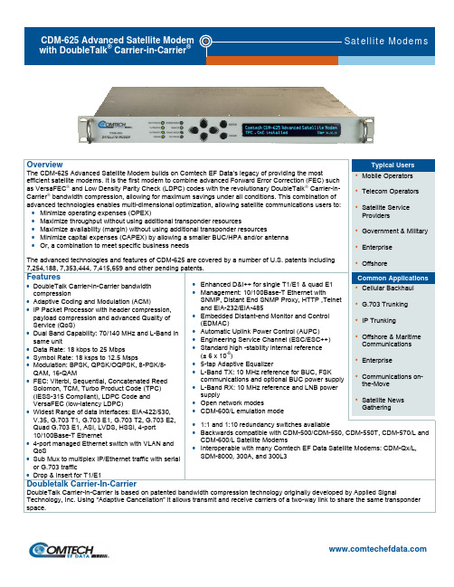
Overview
The CDM-625 Advanced Satellite Modem builds on Comtech EF Data’s legacy of providing the most efficient satellite modems. It is the first modem to combine advanced Forward Error Correction (FEC) such as VersaFEC and Low Density Parity Check (LDPC) codes with the revolutionary DoubleTalk Carrier-inCarrier bandwidth compression, allowing for maximum savings under all conditions. This combination of advanced technologies enables multi-dimensional optimization, allowing satellite communications users to: Minimize operating expenses (OPEX) Maximize throughput without using additional transponder resources Maximize availability (margin) without using additional transponder resources Minimize capital expenses (CAPEX) by allowing a smaller BUC/HPA and/or antenna Or, a combination to meet specific business needs The advanced technologies and features of CDM-625 are covered by a number of U.S. patents including 7,254,188, 7,353,444, 7,415,659 and other pending patents.
Comtech
? 数据率范围从2.4 kbps到20 Mbps
? 中等数据速率业务(IDR)
? 国际卫星通信业务服务
? ESC++
? 内置式远端监控(EDMAC)
? 1:1和1:10冗余开关
? 国内公安系统指导产品(配合CIM25使用)
主要特点
? 2.4 kbps至9.98 Mbps的数据率
? 对称及不对称运行,最大带宽效率
? 支持网状、星状和混合网络拓扑
? 调制类型:BPSK、QPSK、OQPSK、 8-PSK、8-QAM、16 QAM
? 自动上行链路功率控制(AUPC)
系列
CDM-625高级卫星调制解调器以Comtech EF Data的“提供最高效的卫星调制解调器”的传统理念为基础,它是第一款配备高级前向纠错(FEC)技术的调制解调器,例如低密度奇偶校检(LDPC)编码,带有创新的DoubleTalk? Carrier-in-Carrier?带宽压缩级数,可以在任何情况下实现成本节约最大化。
卫星调制解调器CDM570系列
入门级卫星调制解调器,以1 RU尺寸和极具性价比的形式提供了业内领先的性能和灵活性。它是网络运营商、企业用户、业务提供商、广播和政府用户的选择平台。
为了适应低成本终端而设计的调制解调器具有70/140 MHz或L-band IF和EIA-530/-422、 V.35、 EIA-232和G.703数据接口。对于Internet协议(IP)核心应用,提供了一个10/100 BaseT以太网端口的可选IP模块。
主要特点 ຫໍສະໝຸດ ? 同一单元实现70/140 MHz和L波段容量
? 数据率:18 kbps至25 Mbps
JEDEC 625-A
18
7.3 ESD protected workstation ESD ground 靜電防護工作站靜電接地
19
7.4 ESD protected worksurfaces 靜電防護工作台
19
7.4.1 Static dissipative ESD protective worksurfaces 靜電分散、防靜電工作桌
22
9.3.3 Returning rejected ESDS devices to suppliers 歸還判退靜電敏感元件回供應商
22
9.4 Records 紀錄
23
JEDEC Standard No. 625-A REQUIREMENTS FOR HANDLING ELECTORSTATIC-DISCHARGE-SENSITIVE(ESDS)
NOTE – The requirements of this standard are not imposed prior to probe. Prior to porbe, the Manufacturer should take appropriate ESD precautions to minimize damage to devices. 註 – 本標準需求並非強調探針測試前,製造者應採取預防措施減少元件損害於探針測試前。
1
2.1 Applicable users 適用者
1
2.2 Applicable part types 適用文件種類
2
3 Related documents 相關文件
2
3.1 Applicable documents 應用文件
2
4 Terms and definitions 術語及定義
应急通信认证三级题库
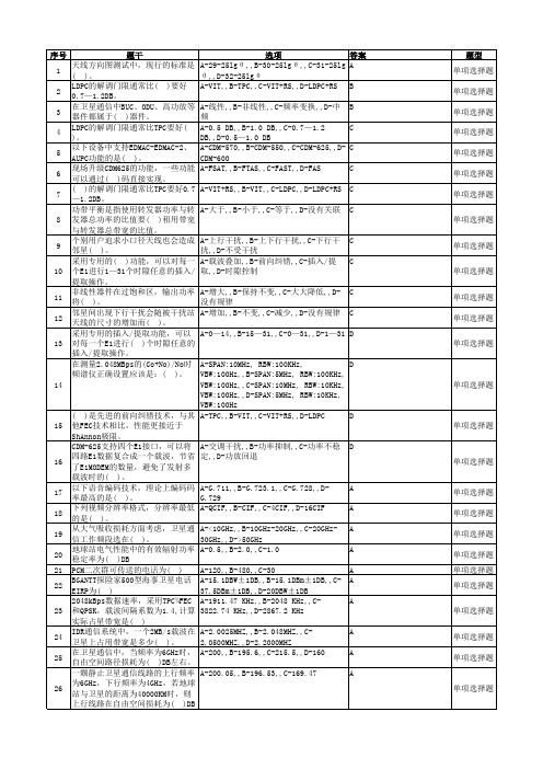
题干 天线方向图测试中,现行的标准是 ( )。 LDPC的解调门限通常比( )要好 0.7—1.2DB。 在卫星通信中BUC、ODU、高功放等 器件都属于( )器件。 LDPC的解调门限通常比TPC要好( )。 以下设备中支持EDMAC-EDMAC-2、 AUPC功能的是( )。 现场升级CDM625的功能,一些功能 可以通过( )码直接实现。 ( )的解调门限通常比TPC要好0.7 —1.2DB。 功带平衡是指使用转发器功率与转 发器总功率的比值要( )租用带宽 与转发器总带宽的比值。 个别用户追求小口径天线也会造成 邻星( )。 采用专用的( )功能,可以对每一 个E1进行1—31个时隙任意的插入/ 提取操作。 非线性器件在过饱和区,输出功率 将( )。 邻星间出现下行干扰会随被干扰站 天线的尺寸的增加而( )。 采用专用的插入/提取功能,可以 对每一个E1进行( )个时隙任意的 插入/提取操作。 在测量2.048MBps的(Co+No)/No时 频谱仪正确设置应该5%,,D-20% A-30,,B-100,,C-无数,,D-50
A A
A-33 DBm,,B-27 DBm,,C-49 DBm,,D-43 A DBm
A-7.9km/s,,B-11.2km/s,,C-16.7km/s
A
A-80000,,B-82000,,C-90000,,D-92000 A
A-8PSK,,B-QPSK,,C-BPSK,,D-A和B A-CRC、FEC,,B-ARQ、CRC,,C-FEC、 ARQ,,D-ARQ、CRC
A A
A-FDD,,B-TDD,,C-FDMA,,D-TDMA
A
A-NCC,,B-IDU,,C-ACU,,D-ODU A-PCM,,B-ADPCM,,C-CELP,,D-AMBE A-PenDing,,B-Running,,C-FAult,,DStopping A-QPSK,,B-QAM,,C-8PSK,,D-4PSK A-TDM,,B-FDM,,C-SCPC,,D-SCDMA A-起能量扩散作用,,B-对传送信息加 密,,C-差错控制,,D-降低时延 A-大,,B-小,,C-不变
cdm625a中文说明书

cdm625a中文说明书摘要:1.产品概述2.安装与设置3.使用方法4.注意事项5.维护与维修正文:【产品概述】cdm625a 是一款高品质的中文说明书,旨在为用户提供详细的操作指南和技术支持。
本说明书包含了产品的各项特性、安装与设置方法、使用方法、注意事项以及维护与维修等方面的内容,帮助用户更好地理解和使用产品。
【安装与设置】在安装cdm625a 之前,请确保您已经仔细阅读了本说明书。
按照以下步骤进行安装:1.检查产品外观是否有损坏,确保所有附件齐全。
2.根据产品尺寸和重量,选择合适的安装位置。
3.按照产品附带的安装指南,进行安装。
安装完成后,进行如下设置:1.输入产品序列号,激活产品。
2.根据实际需求,设置相关参数。
【使用方法】在正确安装并设置好cdm625a 后,您可以开始使用本产品。
以下是一些基本使用方法:1.阅读产品说明书,了解产品各项功能。
2.按照说明书中的操作步骤,进行实际操作。
3.如遇到问题,请参阅本说明书或联系技术支持。
【注意事项】为了确保cdm625a 的正常运行和延长使用寿命,请在使用过程中注意以下几点:1.避免产品受到撞击、摔落等外力损伤。
2.不要在高温、潮湿的环境中长时间使用产品。
3.使用符合产品要求的电源和连接线。
4.定期对产品进行清洁和维护。
【维护与维修】在产品使用过程中,如遇到故障或需要维修,请按照以下步骤进行:1.联系技术支持,提供产品故障现象和相关信息。
2.根据技术支持的建议,进行自我排查或送修。
3.如需维修,请将产品送至指定维修点。
请妥善保存本说明书,以便在日后的使用过程中查阅。
Inconel625

Inconel625合金介绍以及应用INCONEL625是Ni-Cr基固溶强化变形高温合金,以铬、钼和铌为主要固溶强化元素,是最高使用温度可到950℃,该合金从低温到980℃均具有良好的抗拉强度和抗疲劳性能,且加工和焊接性能良好。
合金具有优良的耐腐蚀和抗氧化性能,并且耐盐雾气氛下的应力腐蚀。
广泛应用于制造航空发动机零件、宇航结构部件和化工设备。
主要产品有板材、棒材、丝材、管材、带材和锻件。
INCONEL625合金现在已广泛应用于制造航空和航天发动机机匣、导向叶片、安装边和筒体、燃油总管等零部件,INCONEL625合金无论在海洋气氛还是在非海洋气氛中,腐蚀速度都很小,抗海水腐蚀能力很好。
合金耐各种盐类溶液的腐蚀,具有良好的耐硝酸及磷酸腐蚀的能力。
对加热至沸点以下的盐酸和低溶度的硫酸腐蚀也有相当的抗力。
合金在550℃~700℃长期使用后有一定的时效硬化现象,可导致合金塑性有一些下降。
美标牌号:Inconel625(UNS N06625)、中国牌号:GH3625(GH625)、法国牌号:NC22DNb。
Inconel625执行标准:Inconel 625 的化学成分:合金强化固溶强化加入与基体金属原子尺寸不同的元素(铬、钨、钼等)引起基体金属点阵的畸变,加入能降低合金基体堆垛层错能的元素(如钴)和加入能减缓基体元素扩散速率的元素(钨、钼等),以强化基体。
沉淀强化通过时效处理,从过饱和固溶体中析出第二相(γ'、γ"、碳化物等),以强化合金。
γ'相与基体相同,均为面心立方结构,点阵常数与基体相近,并与晶体共格,因此γ相在基体中能呈细小颗粒状均匀析出,阻碍位错运动,而产生显著的强化作用。
γ'相是A3B型金属间化合物,A代表镍、钴,B代表铝、钛、铌、钽、钒、钨,而铬、钼、铁既可为A又可为B。
镍基合金中典型的γ'相为Ni3(Al,Ti)。
γ'相的强化效应可通过以下途径得到加强:①增加γ'相的数量;②使γ'相与基体有适宜的错配度,以获得共格畸变的强化效应;③加入铌、钽等元素增大γ'相的反相畴界能,以提高其抵抗位错切割的能力;④加入钴、钨、钼等元素提高γ'相的强度。
MEMORY存储芯片TMS320DM642GNZ中文规格书

8TMS320C6745,TMS320C6747SPRS377F –SEPTEMBER 2008–REVISED JUNE 2014Submit Documentation FeedbackProduct Folder Links:TMS320C6745TMS320C6747Device Overview Copyright ©2008–2014,Texas Instruments Incorporated3Device Overview3.1Device CharacteristicsTable 3-1provides an overview of the C6745/6747low power digital signal processor.The table shows significant features of the device,including the capacity of on-chip RAM,peripherals,and the package type with pin count.Table 3-1.Characteristics of the C6745/C6747ProcessorHARDWARE FEATURESC6745C6747PeripheralsNot all peripherals pinsare available at the same time (for moredetail,see the Device Configurations section).EMIFB16bit,up to 128MB SDRAM 16/32bit,up to 256MB SDRAM EMIFAAsynchronous (8-bit bus width)RAM,Flash,NOR,NAND Asynchronous (8/16-bit bus width)RAM,Flash,16bit up to 128MB SDRAM,NOR,NAND Flash Card InterfaceMMC and SD cards supported.EDMA332independent channels,8QDMA channels,2Transfer controllers Timers264-Bit General Purpose (each configurable as 2separate 32-bit timers,1configurable as Watch Dog)UART3(one with RTS and CTS flow control)SPI2(each with one hardware chip select)I 2C2(both Master/Slave)Multichannel AudioSerial Port [McASP]2(each with transmit/receive,FIFO buffer,16/9serializers)3(each with transmit/receive,FIFO buffer,16/9serializers)10/100Ethernet MAC with Management Data I/O 1(RMII Interface)eHRPWM 6Single Edge,6Dual Edge Symmetric,or 3Dual Edge Asymmetric Outputs eCAP 332-bit capture inputs or 332-bit auxiliary PWM outputs eQEP232-bit QEP channels with 4inputs/channel UHPI-1(16-bit multiplexed address/data)USB 2.0(USB0)Full Speed Host Or Device with On-Chip PHY High-Speed OTG Controller with on-chip OTG PHY USB 1.1(USB1)-Full-Speed OHCI (as host)with on-chip PHY General-PurposeInput/Output Port8banks of 16-bit LCD Controller-1RTC-1(32KHz oscillator and seperate power trail.Provides time and date tracking and alarm capability.)PRU Subsystem(PRUSS)2Programmable PRU Cores On-Chip Memory Size (Bytes)320KB RAM 448KB RAMOrganization DSP 32KB L1Program (L1P)/Cache (up to 32KB)32KB L1Data (L1D)/Cache (up to 32KB)256KB Unified Mapped RAM/Cache (L2)DSP Memories can be made accessible to EDMA3,and other peripherals.-ADDITIONAL MEMORY128KB RAMC674x CPU ID +CPU Rev ID Control Status Register (CSR.[31:16])0x1400C674x MegamoduleRevision Revision ID Register (MM_REVID[15:0])0x000051TMS320C6745,TMS320C6747SPRS377F –SEPTEMBER 2008–REVISED JUNE 2014Submit Documentation FeedbackProduct Folder Links:TMS320C6745TMS320C6747Device Overview Copyright ©2008–2014,Texas Instruments Incorporated Table 3-25.General Purpose Input Output Terminal Functions (continued)SIGNAL NAME PIN NOTYPE (1)PULL (2)MUXED DESCRIPTIONPTPZKB GP4USB0_DRVVBUS/GP4[15]-E4O IPD USB0GPIO Bank 4AMUTE1/EPWMTZ/GP4[14]132D4O IPD McASP1,eHRPWM0,eHRPWM1,eHRPWM2AFSR1/GP4[13]166L3I/O IPD McASP1ACLKR1/ECAP2/APWM2/GP4[12]165L2I/O IPD McASP1,eCAP2AHCLKR1/GP4[11]-L1I/O IPD McASP1AFSX1/EPWMSYNCI/EPWMSYNCO/GP4[10]163K4I/O IPD McASP1,eHRPWM0AXR1[9]/GP4[9]-M1I/O IPD McASP1AXR1[8]/EPWM1A/GP4[8]168M2I/O IPD McASP1,eHRPWM1A AXR1[7]/EPWM1B/GP4[7]169M3I/O IPD McASP1,eHRPWM1B AXR1[6]/EPWM2A/GP4[6]170M4I/O IPD McASP1,eHRPWM2A AXR1[5]/EPWM2B/GP4[5]171N1I/O IPD McASP1,eHRPWM2B AXR1[4]/EQEP1B/GP4[4]173N2I/O IPD McASP1,eQEP AXR1[3]/EQEP1A/GP4[3]174P1I/O IPD AXR1[2]/GP4[2]175P2I/O IPD McASP1AXR1[1]/GP4[1]176R2I/O IPD AXR1[0]/GP4[0]1T3I/O IPD GP5EMB_WE_DQM[0]/GP5[15]60K14O IPU EMIFB GPIOBank 5EMB_WE_DQM[1]/GP5[14]85C15O IPU SPI1_SCS[0]/UART2_TXD/GP5[13]8P4O IPU SPI1,UART2SPI1_ENA/UART2_RXD/GP5[12]7R4I IPU AXR1[11]/GP5[11]6T4I/O IPU McASP1AXR1[10]/GP5[10]4N3I/O IPU UART0_TXD/I2C0_SCL/TM64P0_OUT12/GP5[9]/BOOT[9]2R3I IPU UART0,I2C0,BOOT UART0_RXD/I2C0_SDA/TM64P0_IN12/GP5[8]/BOOT[8]3P3O IPU SPI1_CLK/EQEP1S/GP5[7]/BOOT[7]16T6I IPD SPI1,eQEP1,BOOT SPI1_SIMO[0]/I2C1_SDA/GP5[6]/BOOT[6]14N5I/O IPU SPI1,I2C1,BOOT SPI1_SOMI[0]/I2C1_SCL/GP5[5]/BOOT[5]13P5I/O IPU SPI0_SCS[0]/UART0_RTS/EQEP0B/GP5[4]/BOOT[4]9N4I IPU SPI0,UART0,eQEP0,BOOT SPI0_ENA/UART0_CTS/EQEP0A/GP5[3]/BOOT[3]12R5I IPU SPI0_CLK/EQEP1I/GP5[2]/BOOT[2]11T5I IPD SPI0,eQEP1,BOOT SPI0_SIMO[0]/EQEP0S/GP5[1]/BOOT[1]18P6I IPD SPI0,eQEP0,BOOT SPI0_SOMI[0]/EQEP0I/GP5[0]/BOOT[0]17R6I IPD。
MEMORY存储芯片TMS320DM642AGNZ中文规格书

52TMS320C6745,TMS320C6747SPRS377F –SEPTEMBER 2008–REVISED JUNE 2014Submit Documentation FeedbackProduct Folder Links:TMS320C6745TMS320C6747Device Overview Copyright ©2008–2014,Texas Instruments IncorporatedTable 3-25.General Purpose Input Output Terminal Functions (continued)SIGNAL NAME PIN NOTYPE (1)PULL (2)MUXED DESCRIPTION PTPZKB (3)GP7[14]is initially configured as a reserved function after reset and will not be in a predictable state.This signal will only be stable afterthe GPIO configuration for this pin has been ers should carefully consider the system implications of this pin being in an unknown state after reset.GP6EMB_D[15]/GP6[15]74F13I/O IPD EMIFB GPIO Bank 6EMB_D[14]/GP6[14]76E`6I/O IPD EMB_D[13]/GP6[13]78E13I/O IPD EMB_D[12]/GP6[12]79D16I/O IPD EMB_D[11]/GP6[11]80D15I/O IPD EMB_D[10]/GP6[10]82D14I/O IPD EMB_D[9]/GP6[9]83D13I/O IPD EMB_D[8]/GP6[8]84C16I/O IPD EMB_D[7]/GP6[7]62J16I/O IPD EMB_D[6]/GP6[6]63J15I/O IPD EMB_D[5]/GP6[5]64J13I/O IPD EMB_D[4]/GP6[4]66H16I/O IPD EMB_D[3]/GP6[3]68H13I/O IPD EMB_D[2]/GP6[2]70G16I/O IPD EMB_D[1]/GP6[1]72G13I/O IPD EMB_D[0]/GP6[0]73F16I/O IPD GP7EMU[0]/GP7[15]-J5I/O IPU JTAG RTCK/GP7[14](3)157K1I/O IPD General-Purpose IO signal EMB_A[11]/GP7[13]91B12O IPD EMIFB GPIO Bank 7EMB_A[10]/GP7[12]105A9O IPD EMB_A[9]/GP7[11]92C12O IPD EMB_A[8]/GP7[10]94D12O IPD EMB_A[7]/GP7[9]95A11O IPD EMB_A[6]/GP7[8]96B11O IPD EMB_A[5]/GP7[7]97C11O IPD EMB_A[4]/GP7[6]98D11O IPD EMB_A[3]/GP7[5]100A10O IPD EMB_A[2]/GP7[4]101B10O IPD EMB_A[1]/GP7[3]102C10O IPD EMB_A[0]/GP7[2]103D10O IPD EMB_BA[0]/GP7[1]107C9O IPU EMB_BA[1]/GP7[0]106B9O IPU (1)PWR =Supply voltage.3.6.21Reserved and No ConnectTable 3-26.Reserved and No Connect Terminal FunctionsSIGNAL NAMEPIN NO TYPE (1)DESCRIPTION PTP ZKB RSV1-F7-Reserved.(Leave unconnected,do not connect to power orground.)59TMS320C6745,TMS320C6747SPRS377F –SEPTEMBER 2008–REVISED JUNE 2014Submit Documentation FeedbackProduct Folder Links:TMS320C6745TMS320C6747Device Configuration Copyright ©2008–2014,Texas Instruments Incorporated 4.3Pullup/Pulldown ResistorsProper board design should ensure that input pins to the device always be at a valid logic level and not floating.This may be achieved via pullup/pulldown resistors.The device features internal pullup (IPU)and internal pulldown (IPD)resistors on most pins to eliminate the need,unless otherwise noted,for external pullup/pulldown resistors.An external pullup/pulldown resistor needs to be used in the following situations:•Boot and Configuration Pins:If the pin is both routed out and 3-stated (not driven),an external pullup/pulldown resistor is strongly recommended,even if the IPU/IPD matches the desired value/state.•Other Input Pins:If the IPU/IPD does not match the desired value/state,use an external pullup/pulldown resistor to pull the signal to the opposite rail.For the boot and configuration pins,if they are both routed out and 3-stated (not driven),it is strongly recommended that an external pullup/pulldown resistor be implemented.Although,internal pullup/pulldown resistors exist on these pins and they may match the desired configuration value,providing external connectivity can help ensure that valid logic levels are latched on these device boot and configuration pins.In addition,applying external pullup/pulldown resistors on the boot and configuration pins adds convenience to the user in debugging and flexibility in switching operating modes.Tips for choosing an external pullup/pulldown resistor:•Consider the total amount of current that may pass through the pullup or pulldown resistor.Make sure to include the leakage currents of all the devices connected to the net,as well as any internal pullup or pulldown resistors.•Decide a target value for the net.For a pulldown resistor,this should be below the lowest V IL level of all inputs connected to the net.For a pullup resistor,this should be above the highest V IH level of all inputs on the net.A reasonable choice would be to target the V OL or V OH levels for the logic family of the limiting device;which,by definition,have margin to the V IL and V IH levels.•Select a pullup/pulldown resistor with the largest possible value;but,which can still ensure that the net will reach the target pulled value when maximum current from all devices on the net is flowing through the resistor.The current to be considered includes leakage current plus,any other internal and external pullup/pulldown resistors on the net.•For bidirectional nets,there is an additional consideration which sets a lower limit on the resistance value of the external resistor.Verify that the resistance is small enough that the weakest output buffer can drive the net to the opposite logic level (including margin).•Remember to include tolerances when selecting the resistor value.•For pullup resistors,also remember to include tolerances on the IO supply rail.•For most systems,a 1-k Ωresistor can be used to oppose the IPU/IPD while meeting the above ers should confirm this resistor value is correct for their specific application.•For most systems,a 20-k Ωresistor can be used to compliment the IPU/IPD on the boot and configuration pins while meeting the above ers should confirm this resistor value is correct for their specific application.•For more detailed information on input current (I I ),and the low-/high-level input voltages (V IL and V IH )for the device,see Section 5.3,Recommended Operating Conditions.•For the internal pullup/pulldown resistors for all device pins,see the peripheral/system-specific terminal functions table.。
- 1、下载文档前请自行甄别文档内容的完整性,平台不提供额外的编辑、内容补充、找答案等附加服务。
- 2、"仅部分预览"的文档,不可在线预览部分如存在完整性等问题,可反馈申请退款(可完整预览的文档不适用该条件!)。
- 3、如文档侵犯您的权益,请联系客服反馈,我们会尽快为您处理(人工客服工作时间:9:00-18:30)。
CDM-625 与 CDM-600/L对比 (cont’d.)
CDM-600/CDM-600L
管理 EIA-232/485 10/100BaseT Ethernet with SNMP, http & telnet 载波叠加 512 kbps 1 Mbps 2.5 Mbps 5 Mbps 10 Mbps 15 Mbps 20 Mbps 25 Mbps 自适应均衡器 Drop & Insert Open Network D&I++: Single T1/E1 D&I++: Quad E1 高稳定参考源 10 MHz 参考输出 杂散 x With CiM-25
Comtech EF Data Proprietary & Confidential
工作频率
• 50 – 180 MHz (标准配置)
– BNC 接头
• 950 – 1950 MHz (FAST 选项)
– N 型接头 – LNB 供电和10 MHz 参考 – BUC 直流供电(硬件选项), FSK 和 10 MHz 参考
• 数据速率等级
– – – – – 18 kbps to 5 Mbps (Standard) 18 kbps to 10 Mbps (FAST) 18 kbps to 15 Mbps (FAST) 18 kbps to 20 Mbps (FAST) 18 kbps to 25 Mbps (FAST)
– 功率谱密度比要求: +11 to -7 dB
Comtech EF Data Proprietary & Confidential
DoubleTalk 载波叠加
• 需要硬件选项卡
– 卡上不包括CnC许可
• 许可等级
– – – – – – – – 512 kbps (FAST) 1 Mbps (FAST) 2.5 Mbps (FAST) 5 Mbps (FAST) 10 Mbps (FAST) 15 Mbps (FAST) 20 Mbps (FAST) 25 Mbps (FAST)
其他标配功能
• 高稳定内时钟
– ±0.06 ppm (±6.0 x 10⁻⁸), 0 -- 50ºC
• 自适应均衡器
Comtech EF Data Proprietary & Confidential
热备份切换开关
• CRS-300_625
– 1:N 数据切换开关 – TMI/RMI
数据接口
EIA-422/V.35, EIA-232
与“载波叠加” + TPC解决方案相比,能够更加有效地降低 OPEX和CAPEX
Comtech EF Data Proprietary & Confidential
CDM-625高级卫星Modem
• 高级功能选项
– – – – DoubleTalk 载波叠加 集成的LDPC和TPC编解码 70/140 MHz 和 L-band 并存于一个机箱 最宽范围的数据接口
x x x x (CIC-20)
x x x x (CIC-60, Passive Adapter) x
G.703 T1/E1/T2/E2
Quad E1 4 x 10/100BaseT 帧头
x
x
x (FAST) x
x
x
Comtech EF Data Proprietary & Confidential
– TPC 码率
Rate 5/16 BPSK Rate 21/44 BPSK/QPSK/OQPSK Rate 3/4 QPSK/OQPSK/8-PSK/8-QAM/16-QAM Rate 7/8 QPSK/OQPSK/8-PSK/8-QAM/16-QAM Rate 0.95 QPSK/OQPSK/8-PSK/8-QAM
开网和闭网
– 8-PSK/TCM 2/3 ,符合 IESS-310 (8-PSK 是FAST选项) – 集成的TPC (2nd Gen) 和 LDPC 编解码 (硬件, FAST 选项)
Comtech EF Data Proprietary & Confidential
集成的TPC 和 LDPC 编解码
x
x (Option Module) x (Option Module) x (Option Module) x x (LR TPC, LDPC) x (LDPC) x (HR TPC, LDPC)
x
集成的 TPC/LDPC 编解码器 (可选模块) Available Next Release x (标配) x (FAST) x (FAST) x (FAST) x (FAST)
Comtech EF Data Proprietary & Confidential
调制和前向纠错
• 调制方式
– – – – BPSK QPSK/OQPSK 8-PSK/8-QAM (FAST) 16-QAM (FAST)
• 前向纠错
– Viterbi – Viterbi + Reed Solomon
Comtech EF Data Proprietary & Confidential
管理
• 10/100BaseT 以太网
– SNMP – http – telnet
• EIA-232/485 • EDMAC/EDMAC-2 • AUPC
Comtech EF Data Proprietary & Confidential
Comtech EF Data Proprietary & Confidential
DoubleTalk 载波叠加
• 更强的性能
– – – – 对符号速率比没有要求 改进的解调门限性能 与LDPC结合使用,优化效果更好 更强的非对称处理能力
• 功率比根据功率谱密度,不再是绝对功率(如 CDM-Qx)
CDM-600/L 仿真模式
• CDM-625 可工作再CDM-600 或 CDM-600L 仿真模式 • CDM-625仿真CDM-600/L的远控命令和功能 • 用于CDM-625替换一个1:N CDM-600/L系统中 的一台Modem
Comtech EF Data Proprietary & Confidential
– 需要扩展卡 Requires Optional Expansion Card – LDPC 码率
Rate 1/2 BPSK/QPSK/OQPSK Rate 2/3 QPSK/OQPSK/8-PSK/8-QAM Rate 3/4 QPSK/OQPSK/8-PSK/8-QAM/16-QAM
主用接口卡
CRS-320 or CRS-340
备份接口卡
G.703 T1/E1, T2/E2 HSSI to/from LVDS ASI Quad E1 Ethernet – 单口(网桥模式)
CRS-330 or CRS-340 CRS-370 CRS-325 CRS-365D CRS-316 (Not Yet Released)
– 1:1 70/140MHz中频切换开关 – Y型电缆解决数据接口问题
Comtech EF Data Proprietary & Confidential
热备份切换开关
• CRS-280/L 中频切换开关 • CRS-150 不能用于CDM-625
Comtech EF Data Proprietary & Confidential
Comtech EF Data Proprietary & Confidential
CDM-625 主要特点
• 数据速率: 18 kbps -- 25 Mbps
– 符号速率: 18 ksps -- 12.5 Msps
• • • •
支持DoubleTalk载波叠加处理,压缩占用带宽 集成TPC/LDPC 编解码 支持70/140 MHz 和 L-band,接收和发射独立 调制解调方式: BPSK、QPSK/OQPSK、8-PSK/8QAM、16-QAM • 支持开网工作模式 • CDM-600 模式
ADVANCED COMMUNICATION SOLUTIONS
CDM-625 Advanced Satellite Modem
Naresh Jain
CDM-625 –高级卫星Modem
• CDM-625 继承了了CEFD一贯的“高带宽”效率的 卫星MODEM的设计思想 • 另一个业内第一
– 第一台同时支持“载波叠加”和LDPC功能的卫星Modem 。
• 独立的接收和发射
– 能够发射70/140 MHz 并接收L-band,或相反的方 式
Comtech EF Data Proprietary & Confidential
数据速率/符号速率
• 18 ksps to 12.5 Msps • 18 kbps to 25 Mbps
– 受限于调制方式、纠错方式和数据接口
CDM-625
18 kbps to 25 Mbps 18 ksps to 12.5 Msps 同一个机箱中包含70/140 MHz 和LBand , L-Band 是FAST选项 x (标配) x (FAST) x (FAST) x (FAST) x (FAST)
8-PSK/8-QAM
16-QAM
x (FAST)
Comtech EF Data Proprietary & Confidential
数据接口和连接器
• 最宽范围的数据接口
– 4个 10/100 以太网接口 [RJ-45]
2层交换
– HSSI (最高支持25 Mbps) [DB-25]