时钟无毛刺切换电路
免毛刺时钟切换电路设计方法
免毛刺时钟切换电路设计方法基于网上资料整理,并进一步作了分析。
这篇文章讲述了时钟切换的时候毛刺(glitch)带来的危害,以及如何设计防止毛刺发生的时钟切换电路。
但是没有讲到电路设计的构思从何而来,大家看了之后知道直接用这个电路,但是假如不看这篇文章,自己从头设计还是无从下手。
在这里,我换另外一个角度,通过电路设计技巧来阐述防毛刺时钟切换电路的设计思路。
希望看过之后,不用参考文章就能够自己设计出这个电路。
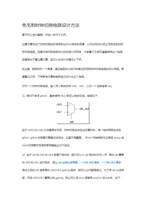
对于一个时钟切换电路,输入两个异步时钟clk0、clk1,以及一个选择信号sel。
(1) 假设不考虑glitch,直接使用Mux就可以完成切频。
电路如下:由于clk0/clk1/sel之间是异步关系,时钟切换会发生在任意时刻,有一定的概率会发生glitch. glitch的危害文章里已经详述,这里不再重复。
Glitch可能导致无法满足setup或hold时序要求而导致寄存器输出为不定态。
(2) 由于sel和clk0和clk1都是不同步的,我们可以从sel同步的方向入手,假如sel需要和clk0和clk1进行同步,那么sel必须分成两路,一个和clk0同步,一个和clk1同步,同步之后的sel信号再和clk0/clk1 gating起来,就可以让问题简单化。
为了将sel分成两路,并且clk0/clk1需要分别gating, 那么可以将mux逻辑用and/or设计出来,如下:当然此Mux电路还可以用两个or加上一个and来实现,都可以。
注意G0和G1两点就是分别对clk0和clk1进行gating. 将来会在G0/G1点插入同步DFF.(3) 将上面电路拆开成两部分,一部分电路通过sel产生sel+和sel-两路,另一部分电路是gating mux电路, 如下:只需要将sel-接上G0, sel+接上G1就是一个mux电路。
将电路分开,是为了后续技巧性的功能替换。
(4) 将part0电路换成同样功能的带反馈的组合电路(为何要这样做,属于电路设计直觉和技巧。
A功能数字钟的电路设计

功能数字钟的电路设计数字钟是采用数字电路实现“时”、“分”、“秒”数字显示的计时装置。
钟表的数字化在提高报时精度的同时,也大大扩展了它的功能,诸如定时自动报警、按时自动打铃、时间程序自动控制、定时广播、定时启闭路灯等。
因此,研究数字钟及扩大其应用,有着非常现实的意义。
1、设计目的1)掌握数字钟的设计、组装与调试方法。
2)熟悉集成电路的使用方法。
2、设计任务与要求1)时钟显示功能,能够以十进制显示“时”、“分”、“秒”。
2)具有校准时、分的功能。
3)整点自动报时,在整点时,便自动发出鸣叫声,时长1s。
选做:1)闹钟功能,可按设定的时间闹时。
2)日历显示功能。
将时间的显示增加“年”、“月”、“日”。
3、数字钟的基本原理及电路设计一个具有计Array时、校时、报时、显示等基本功能的数字钟主要由振荡器、分频器、计数器、译码器、显示器、校时电路、报时电路等七部分组成。
石英晶体振荡器产生的信号经过分频器得到秒脉冲,秒脉冲送入计数器计数,计数结果通过“时”、“分”、“秒”译码器译码,并通过显示器显示时间。
数字钟的整机逻辑框图如下:图 1数字钟整机逻辑图振荡器方案一:由集成电路定时器555与RC组成的多谐振荡器作为时间标准信号源。
图 2 555与RC 组成的多谐振荡器图 分析:图中的C2为保护电容,其取值并没有什么要求。
在本设计中,我假设输出的脉冲的占空比为2/3,并且把555与RC 组成的多谐振荡,参考书本上的方案得出占空比3222121=++=R R R R q 故得到R1=R2。
又有电路的振荡周期T=T1+T2=(R1+2R2)Cln2得T=(R1+2R2)Cln2=103-S 。
我在实验中取电容为10nf 。
带入式中,可以得出R1=R2=48K Ω。
在这里取两个47K Ω电阻和滑动电阻2K Ω。
仿真结果如图所示,误差还是比较低的。
方案二:石英晶体振荡器。
石英晶体振荡器的特点是振荡频率准确、电路结构简单、频率易调整,它是电子钟的核心,用它产生标准频率信号,再由分频器分成秒时间脉冲。
数字时钟各单元电路的设计方案及原理说明

数字时钟各单元电路的设计方案及原理说明数字时钟是现代生活中常见的时间显示工具,它通过使用数字来表示小时和分钟。
而数字时钟的核心组成部分则是由各个数字显示单元电路组成的。
在本文中,我将为您介绍数字时钟各单元电路的设计方案及原理说明,希望能帮助您更深入地了解数字时钟的工作原理。
我们需要了解数字时钟的基本原理。
数字时钟使用了七段显示器来显示数字,每个数字由七个LED(Light Emitting Diode)组成,分别表示了该数字的不同线条。
为了控制七段显示器显示特定的数字,我们需要设计相应的驱动电路。
1. 数字时钟的驱动电路设计方案a. 时钟信号生成器:数字时钟需要一个稳定的时钟信号来驱动各个单元电路,通常使用晶振电路来生成精确的时钟信号。
b. 时分秒计数器:用于计数时间,并将计数结果转化为可以驱动七段显示器的信号。
时分秒计数器可以使用计数逻辑电路来实现,其中包括触发器和计数器芯片等。
c. 译码器:译码器用于将计数器输出的二进制数据转换为可以驱动七段显示器的控制信号。
根据不同的数字,译码器会选通对应的七段LED。
2. 数字时钟的各单元电路原理说明a. 时钟信号生成器的原理:晶振电路通过将晶振与逻辑电路相连,通过振荡来生成稳定的时钟信号。
晶振的振荡频率决定了时钟的精确度,一般使用32.768kHz的晶振来实现。
b. 时分秒计数器的原理:时分秒计数器使用触发器和计数器芯片来实现,触发器可以保存二进制的计数值,并在时钟信号的作用下进行状态切换。
计数器芯片可以根据触发器的状态进行计数和重置操作。
c. 译码器的原理:译码器根据计数器输出的二进制数据选择对应的七段LED。
七段LED通过加电来显示数字的不同线条,然后通过译码器的工作,将二进制数据转换为驱动七段LED的信号。
通过以上的设计方案和原理说明,我们可以更好地理解数字时钟各单元电路的工作原理。
数字时钟通过时钟信号生成器来提供稳定的时钟信号,时分秒计数器记录并计算时间,译码器将计数结果转化为可以驱动七段显示器的信号。
时钟电路、布线和端接

时钟电路的电磁干扰源
01
时钟信号的辐射干扰
时钟信号在传输过程中可能会产生辐射干扰,影响周围电路的正常工作。
02
电源线传导干扰
时钟电路中的电流变化会产生电压波动,通过电源线传播,影响其他电
路的稳定性。
03
元器件的开关噪声
时钟电路中的开关元件在切换过程中会产生瞬态电流和电压,形成电磁
干扰。
电磁兼容性的设计原则
时钟电路在通信系统中的应用
同步通信
时钟电路为通信系统提 供稳定的时钟信号,确 保通信设备间的数据传 输同步,避免数据冲突 和丢失。
信号处理
时钟电路用于产生和处 理通信系统中的信号, 如调制解调、编解码等, 提高信号质量和传输效 率。
定时与控制
时钟电路用于实现通信 系统的定时和控制功能, 如定时发送数据、控制 数据流量等。
接地设计
滤波技术
屏蔽技术
布局布线
合理的接地方式可以有 效降低电磁干扰的影响,
提高电路的稳定性。
在时钟线路上使用滤波 器可以滤除不必要的电 磁噪声,提高信号质量。
利用金属屏蔽体隔离敏 感区域,减少电磁干扰
的传播。
合理的电路布局和布线 可以降低电磁干扰的影 响,提高电路的稳定性。
06
时钟电路的应用与发展趋势
相位噪声
时钟信号的相位噪声是指在时钟信号频谱上周围的噪声,它会影响时 钟信号的质量。
时钟信号的测试方法
1 2
示波器测试
使用示波器观察时钟信号的波形,测量频率、抖 动等参数。
频谱分析仪测试
使用频谱分析仪测量时钟信号的相位噪声。
3
误码率测试
通过在时钟信号上加入噪声,观察误码率的变化, 评估时钟信号的质量。
时序电路的作用

时序电路的作用1. 时序电路简介时序电路是指一类能够按照预定的时间顺序进行状态切换的电路。
它由各种触发器、计数器和时钟信号等组成,广泛应用于数字系统中,用于控制和调度各个部件的运行顺序。
时序电路在数字系统中起着至关重要的作用。
2. 时序电路的分类2.1 同步时序电路同步时序电路是指通过同步信号进行状态切换的电路。
同步时序电路中,各个触发器和计数器的状态变化是同步进行的,由时钟信号来驱动。
典型的同步时序电路包括时钟分频器和状态机等。
同步时序电路通过统一的时钟信号来保证各个部件的同步运行,能够提高系统的稳定性和可靠性。
2.2 异步时序电路异步时序电路是指通过异步信号进行状态切换的电路。
异步时序电路中,各个触发器和计数器的状态变化是独立进行的,不需要时钟信号来驱动。
典型的异步时序电路包括门闩电路和脉冲生成电路等。
异步时序电路能够根据特定的输入信号实时响应,具有较高的灵活性和响应速度。
3. 时序电路的作用时序电路在数字系统中发挥着重要的作用,具有以下几个方面的功能:3.1 控制信号的生成和延时时序电路能够根据时钟信号和输入信号生成各个部件的控制信号,并对信号进行延时处理。
通过时序电路可以实现复杂的控制逻辑,对各个部件的运行顺序和时序进行精确控制,确保数字系统的正常工作。
3.2 数据的存储和传递时序电路中的触发器和计数器等部件能够存储和传递数据。
触发器可以将输入的数据存储起来,并在时钟信号的作用下将数据传递给下一个触发器或计数器,从而实现数据的传输和处理。
时序电路可以在不同的时钟周期中完成各个数据操作,确保数据的正确性和稳定性。
3.3 状态的控制和转换时序电路中的状态机可以对系统的状态进行控制和转换。
状态机能够根据输入信号的变化和时钟信号的触发,按照预定的状态转移规则进行状态的切换。
通过状态机的设计,可以实现复杂的状态控制和决策逻辑,使系统能够按照特定的流程和顺序进行运行。
3.4 时序逻辑的实现时序电路能够实现各种时序逻辑的功能。
第三章时钟电路与复位电路ppt课件

2.5 I/O端口电路与电气特性
❖ P0、P1、P2、P3
既有字节地址,也有位地址,对相应的地址单元 进行写操作,就完成了相应端口的输入/输出操作
❖ 1个全双工的串行I/O口,用于扩展I/O口或用作串
行异步通信(第五章专门介绍)
2.5.1 I/O接口内部电路结构 P0端口
➢双向I/O端口 ➢数据/地址复用总线
89C51
振荡电路
89C51(CHMOS工艺)的 外部输入为X1,X2悬空
HMOS工艺的芯片
2.基本时序单位
❖ 振荡周期:1/fOSC 最小的时序单位
❖ 状态(S)周期:2/fOSC 包含两个节拍(P1、P2),一个节拍为1个振荡周期。
❖ 机器周期MC: 12/fOSC 6个状态,S1-S6,12个节拍(S1P1、S1P2、S2P1、 S2P2…),12个振荡周期
CMOS与TTL电平关系表
P3.0 RXD 串行接收 P3.1 TXD 串行发送
P3.4 T0 计数0输入 P3.5 T1 计数1输入
P3.2 /INT0 外中断0输入 P3.6 /WR 写信号引脚
P3.3 /INT1 外中断1输入 P3.7 /RD 读信号引脚
2.5.2 I/O端口负载能力
P0口每一位输出可驱动8个LSTTL负载,当作地 址/数据输出时是标准的三态双向口。当作为通用I/O 接口使用时是开漏输出,只有灌负载能力没有拉负载 能力。要想得到拉负载能力需外接一个上拉电阻才行。
低功耗工作方式
低功耗工作方式
➢进入待机:使IDL=1即可。
➢进入掉电:使PD=1即可,进入后,可将VCC降至 2V(保持RAM、SFR),但在退出掉电时,先使电 压升至正常电压。
时间继电器 原理

时间继电器原理
时间继电器是一种能够根据预设的时间参数来控制电路的继电器。
它通常由电磁继电器和时钟电路组成。
时间继电器的工作原理如下:首先,通过时钟电路提供的时钟脉冲,驱动继电器的触点切换。
触点有两个状态:一个是常闭状态,另一个是常开状态。
通常,触点处于常闭状态,当时钟电路提供的脉冲到达预设的时间点时,触点切换到常开状态,从而切断或接通电路。
具体来说,时间继电器的工作原理如下:在时钟电路中,一个定时器会不断地产生固定频率的脉冲信号。
这些脉冲信号通过计数器进行计数,并与预设的时间参数进行比较。
当计数器的值与预设值相等时,计数器会触发触发器,使继电器的触点切换状态。
在电磁继电器中,触点的切换通过控制电流的流向来实现。
当触点处于常闭状态时,控制电路的电流通过电磁线圈,使线圈产生磁场,将触点吸引住,从而闭合电路。
当触点切换到常开状态时,电流停止流过电磁线圈,线圈的磁场消失,触点恢复到常开状态,电路断开。
时间继电器广泛应用于定时控制领域,如照明设备、温度控制、电动机启停等。
它的工作原理可靠且易于调节,能够精确控制电路的开关时间,提高电路的稳定性和安全性。
verilog基本电路设计(包括:时钟域同步、无缝切换、异步fifo、去抖滤波))

Verilog基本电路设计(包括:时钟域同步、无缝切换、异步FIFO、去抖滤波))Verilog基本电路设计共包括四部分:单bit跨时钟域同步时钟无缝切换异步FIFO去抖滤波Verilog基本电路设计之一: 单bit跨时钟域同步(帖子链接:/thread-605419-1-1.html)看到坛子里不少朋友,对于基本数字电路存在这样那样的疑惑,本人决定开贴,介绍数字电路最常见的模块单元,希望给初学者带来帮助,也欢迎大佬们前来拍砖。
如果想要做数字设计,下面这些电路是一定会碰到的,也是所有大型IP,SOC设计必不可少的基础,主要包括异步信号的同步处理,同步FIFO,异步FIFO,时钟无缝切换,信号滤波debounce等等,后面会根据大家反馈情况再介绍新电路。
首先介绍异步信号的跨时钟域同步问题。
一般分为单bit的控制信号同步,以及多bit的数据信号同步。
多bit的信号同步会使用异步FIFO完成,而单bit的信号同步,又是时钟无缝切换电路以及异步FIFO电路的设计基础,这里先介绍单bit信号同步处理。
clka域下的信号signal_a,向异步的clkb域传递时,会产生亚稳态问题。
所有的亚稳态,归根结底就是setup/hold时间不满足导致。
在同一个时钟域下的信号,综合以及布线工具可以在data路径或者clock路径上插入buffer使得每一个DFF的setup/hold时间都满足;但是当signal_a在clkb域下使用时,由于clka与clkb异步,它们的相位关系不确定,那么在clkb的时钟沿到来时,无法确定signal_a此时是否处于稳定无变化状态,也即setup/hold时间无法确定,从而产生亚稳态。
这种异步信号在前后端流程里面是无法做时序分析的,也就是静态时序分析里常说的false_path。
消除亚稳态,就是采用多级DFF来采样来自另一个时钟域的信号,级数越多,同步过来的信号越稳定。
对于频率很高的设计,建议至少用三级DFF,而两级DFF同步则是所有异步信号处理的最基本要求。
一个时钟异步切换无毛刺电路
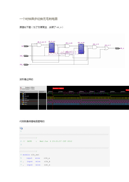
一个时钟异步切换无毛刺电路原理如下图(为了方便简洁,去掉了rst_n)波形是这样的代码就是根据电路图写的1//////////////////////////////////////////////////////////////////////////// ///////////////2// DATE : Wed Jun 6 23:31:57 CST 20123//////////////////////////////////////////////////////////////////////////// ///////////////4module clk_sw(5input wire clk_a6 , input wire clk_b7 , input wire rst_n8 , input wire sel9 , output wire clk_o10);11//////////////////////////////////////////////////////////////////////////// ///////////////12// variable declaration13reg clk_a_en ;14reg clk_b_en ;15//////////////////////////////////////////////////////////////////////////// ///////////////16// logic17always @(posedge clk_a or negedge rst_n) begin18if(~rst_n) clk_a_en <= 1'b0 ;19else clk_a_en <= ~sel & ~clk_b_en ;20end21always @(posedge clk_b or negedge rst_n) begin22if(~rst_n) clk_b_en <= 1'b0 ;23else clk_b_en <= sel & ~clk_a_en ;24end25assign clk_o = (clk_a & clk_a_en) | (clk_b & clk_b_en) ;26//////////////////////////////////////////////////////////////////////////// ///////////////2728endmodule// CREATED by poiu_elab@12072930//////////////////////////////////////////////////////////////////////////// ///////////////testbench是这样的1//////////////////////////////////////////////////////////////////////////// ///////////////2// DATE : Wed Jun 6 23:42:58 CST 20123//////////////////////////////////////////////////////////////////////////// ///////////////4 `define CLK_A_CYCLE 235 `define CLK_B_CYCLE 476module tb();7//////////////////////////////////////////////////////////////////////////// ///////////////8// variable declaration9reg clk_a ;10reg clk_b ;11reg rst_n ;12reg sel ;13wire clk_o ;14//////////////////////////////////////////////////////////////////////////// ///////////////15// stimulation generation16initial forever #(`CLK_A_CYCLE/2) clk_a = ~clk_a;17initial forever #(`CLK_B_CYCLE/2) clk_b = ~clk_b;18initial begin19 rst_n = 1'b0 ;20 clk_a = 1'b1 ;21 clk_b = 1'b1 ;22 sel = 1'b0 ;23 #500;24 rst_n = 1'b1 ;25 #500;26 #({$random}%13+500);27 sel = ~sel ;28 #({$random}%23+500);29 sel = ~sel ;30 #({$random}%33+500);31 sel = ~sel ;32 #({$random}%43+500);33 sel = ~sel ;34 #({$random}%53+500);35 sel = ~sel ;36 #({$random}%63+500);37 sel = ~sel ;38 #({$random}%73+500);39 sel = ~sel ;40 #({$random}%83+500);41 sel = ~sel ;42 #({$random}%93+500);43 sel = ~sel ;44 #({$random}%13+500);45 sel = ~sel ;46 #({$random}%23+500);47 sel = ~sel ;48 #({$random}%33+500);49 sel = ~sel ;50 #({$random}%43+500);51 sel = ~sel ;52 #({$random}%53+500);53 sel = ~sel ;54 #({$random}%63+500);55 sel = ~sel ;56 #({$random}%73+500);57 sel = ~sel ;58 #({$random}%83+500);59 sel = ~sel ;60 #({$random}%93+500);61 sel = ~sel ;62 #5000;63$stop;64end65//////////////////////////////////////////////////////////////////////////// ///////////////66// module instaniation67clk_sw u_clk_sw(68 .clk_a ( clk_a )69, .clk_b ( clk_b )70, .rst_n ( rst_n )71, .sel ( sel )72, .clk_o ( clk_o )73);74//////////////////////////////////////////////////////////////////////////// ///////////////7576endmodule// CREATED by poiu_elab@12077778//////////////////////////////////////////////////////////////////////////// ///////////////这里的核心就是你的sel发生翻转的时候,首先肯定是在本时钟域内的clk_en会先变低(invalid),之后才会使得另外时钟域内的clk_en变高(valid),这时另外一个时钟域内的时钟才能和clk_en相与输出。
时钟自动校准电路及方法
时钟自动校准电路及方法时钟自动校准电路及方法是一种用于确保时钟准确性和稳定性的系统,通常应用于各种电子设备中。
以下是关于时钟自动校准电路及方法的50条详细描述:1. 时钟自动校准电路基本原理是利用外部参考信号或者内部振荡器信号,通过反馈控制来调整时钟频率,以保持时钟的准确性。
2. 该电路通常包括一个比较器,用于将参考信号与时钟信号进行比较,并产生一个误差信号。
3. 误差信号会被传递给一个数字控制电路,根据误差信号的大小和方向来调整时钟的频率。
4. 最常见的自动校准方法是通过PLL(锁相环)技术来实现,其中反馈控制信号会调整振荡器的频率,使其与参考信号保持同步。
5. 该电路还可以包括一个数字-模拟转换器(DAC),用于将数字控制信号转换为模拟电压信号,从而调整振荡器的频率。
6. 时钟信号的频率调整可以通过微调频率合成器的控制电压实现。
这样可以在精确度和稳定性之间进行权衡。
7. 在某些情况下,外部参考信号可能是GPS信号或者其他可靠的时钟源,以确保系统时钟与外部参考保持同步。
8. 除了频率校准,电路还可以进行相位校准,确保时钟的相位与参考信号保持一致。
9. 自动校准电路通常会包括一个反馈环路,用于动态地调整时钟频率和相位,以应对温度变化、老化和其他外部干扰因素。
10. 电路还可以包括一个温度传感器,用于监测环境温度变化,并根据温度变化来调整时钟频率,以确保在不同温度下时钟的准确性。
11. 时钟自动校准电路的设计需要考虑对系统的干扰最小化,以确保在调整时钟频率时不会引入额外的噪音或抖动。
12. 特定的校准算法或逻辑可以应用于数字控制电路,以确保校准的稳定性和快速响应性。
13. 电路设计应考虑功耗和成本等因素,以确保在保持时钟准确性的不会引入过多的额外开销。
14. 时钟自动校准电路还应具有自我诊断的功能,以实时监测时钟的性能,并在发现异常情况时进行自动修正。
15. 对于某些特殊应用,时钟自动校准电路还可以具有多通道输入和输出,以确保对多个时钟信号进行同步校准。
如何实现在速故障点的测试
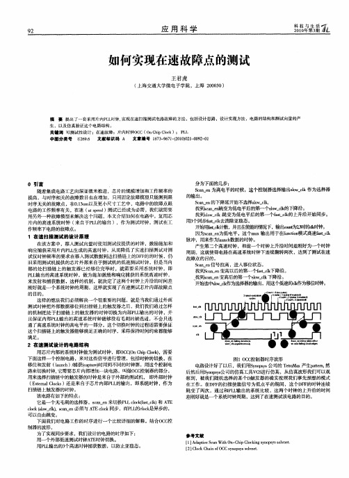
2 在速 溯试 设计 的 电路 结构 用芯片内部 的系统时钟做为测试 时钟 ,lO CO h l k,  ̄ C (n lC a) 需要 P Cp o 下面这样一个控制电路 , 来对这些信号进行管理 ,包括时钟 的切换 , 在 移位和发射 (anh 脯 获( p r时用到不 同的时钟源 , 1 c) u c te au ) 用这个控制 电 路来切换时钟, 它需要芯片内部增加一块电路 ,叫做O C C 控制器的部分 , 用来选择扫描链 中的触发器的时钟是来 自于外部的测试机, 即外部时钟 ( x r l l k) Etn o s 还是来 自于芯片内部P L e aC c L 的输出 ,即系统时钟 , 为 作
分为下面的几步 :
Sa n cne 为高 电平的时候 ,这个控制器选择输/sw_k作为选择器  ̄l _l o c
的输出。 Sa n c e 的下降延开始不选择s w c , n l _l o k
1 在速 扫描 测试 的设 计原理
在该方案中 , 移人测试 向量时使用测试仪提供的时钟 , 激励施加和 响应捕获采用片内P J l 生成的高速时钟 ,从而降低了实速扫描测试对测 L 试仪 时钟频率的要求在移人测试数据到达扫描链上的D F F 的的时候 , 仍 旧采用测试机提供的芯片外部来 自于测试机的低速测试时钟 ,但是当内 部的处扫描链上的触发器 已经移位完毕时 ,就需要采用系统 时钟 ,即 P I 出的高速系统时钟 , 为施加激励和响应捕获 的系统高速时钟 , L简 做 来发射和捕获数据 ,这样 的机制 ,就决定 了这两个时钟上升沿 的时间差 刚好就是一个系统时钟的周期 ,这样就实现了在速测试芯片内部故障 点 的目的。 这样 的想法我们必须解决一个很重要的问题 ,就是当我们通过外面
- 1、下载文档前请自行甄别文档内容的完整性,平台不提供额外的编辑、内容补充、找答案等附加服务。
- 2、"仅部分预览"的文档,不可在线预览部分如存在完整性等问题,可反馈申请退款(可完整预览的文档不适用该条件!)。
- 3、如文档侵犯您的权益,请联系客服反馈,我们会尽快为您处理(人工客服工作时间:9:00-18:30)。
Techniques to make clock switching glitch freeFrom:/articles/exit/?id=5827&url=http://www.eetime /story/OEG20030626S0035Rafey MahmudWith more and more multi-frequency clocks being used in today's chips, especially in the communications field, it is often necessary to switch the source of a clock line while the chip is running. This is usually implemented by multiplexing two different frequency clock sources in hardware and controlling the multiplexer select line by internal logic.The two clock frequencies could be totally unrelated to each other or they may be multiples of each other. In either case, there is a chance of generating a glitch on the clock line at the time of the switch. A glitch on the clock line is hazardous to the whole system, as it could be interpreted as a capture clock edge by some registers while missed by others.In this article, two different methods of avoiding a glitch at the output clock line of a switch are presented. The first method is used when clocks are multiples of each other, while the second deals with clocks totally unrelated to each other.The problem with on-the-fly clock switchingFigure 1 shows a simple implementation of a clock switch, using an AND-OR type multiplexer logic.The multiplexer has one control signal, named SELECT, which either propagates CLK0 to the output when set to "zero" or propagates CLK1 to the output when set to "one." A glitch may be caused due to immediate switching of the output from Current Clock source to the Next Clock source, when the SELECT value changes. Current Clock is the clock source currently selected while Next Clock is the clock source corresponding to the new SELECT value.The timing diagram in Figure 1 shows how a glitch is generated at the output, OUT CLOCK, when the SELECT control signal changes. The problem with this kind of switch is that the switch control signal can change any time with respect to the source clocks, thus creating a potential for chopping the output clock or creating a glitch at the output.The select control signal is most likely generated by a register driven by either of the two source clocks, which means that either it has a known timing relationship to both clocks, if both clocks are multiples of each other, or it may be asynchronous to at least one clock, if source clocks are not related in any way.Switching during either clock's high state needs to be avoided without having any idea about the frequencies or phase relationship of these clocks. Fixed delay can be used to induce the gap between the start and stop time of the two source clocks, but only if a fixed relationship exists between the two clock sources. It cannot be used where either the input frequencies are not known, or the clocks are not related.Figure 1 -- Clock switching multiplexerGlitch protection for related clock sourcesA solution to prevent glitch at the output of a clock switch where source clocks are multiples of each other is presented in Figure 2. A negative edge triggered D flip-flop is inserted in the selection path for each of the clock sources. Registering the selection control at negative edge of the clock, along with enabling the selection only after other clock is de-selected first, provides excellent protection against glitches at the output.Registering the select signal at negative edge of the clock guarantees that no changes occur at the output while either of the clocks is at high level, thus protecting against chopping the output clock. Feedback from one clock's selection to the other enables the switch to wait for de-selection of the Current Clock before starting the propagation of the Next Clock, avoiding any glitches.The figure 2 timing diagram shows how the transition of the SELECT signal from 0 to 1 first stops propagation of CLK0 to the output at the proceeding falling edge of CLK0, then starts the propagation of CLK1 to the output at following negative edge of CLK1.There are three timing paths in this circuit that need special consideration — the SELECT control signal to either one of the two negative edge triggered flip flops, the output of DFF0 to input of DFF1, and the output of DFF1 to the input of DFF0. If the signal on any of these three paths changes at the same time as the capturing edge of the destination flip flop's clock, there is a small chance that the output of that register may become meta-stable, meaning it may go to a state between an ideal "one" and an ideal "zero."A meta-stable state can be interpreted differently by the clock multiplexer and the enable feedback of the other flip flop. Therefore, it is required that capturing edges of both flip flops and the launch edge of the SELECT signal should be set apart from each other to avoid any asynchronous interfacing. This can be easily accomplished by using proper multi-cycle hold constraints or minimum delay constraints, as the timing relationship is known between the two clocks.Figure2 -- Glitch-free clock switching for related clocksFault toleranceAt chip startup time, both flip flops DFF0 and DFF1 should be reset to the "zero" state so that neither one of the clocks is propagated initially. By starting both flip flops in "zero" state, fault tolerance is built into the clock switch.Let's say that one of the clocks was not toggling due to a fault at startup time. If the flip flop associated with the faulty clock had started up in "one" state, it would prevent the selection of other clockas the Next Clock, and its own state is not changeable due to lack of a running clock. By starting both flip flops in "zero" state, even if one of the source clocks is not running, there is still the ability to propagate the other good clock to the output of the switch.Glitch protection for unrelated clock sourcesThe previous method of avoiding a glitch at the output of a clock switch requires the two clock sources to be multiples of each other, such that user can avoid signals to be asynchronous with either one of the clock domains. There is no mechanism to handle asynchronous signals in that implementation.This leads to the second method of implementing the clock switch with synchronizer circuits to avoid potential meta-stability caused by asynchronous signals. The source of asynchronous behavior could either the be SELECT signal or the feedback from one clock domain to the other, when the two clock sources are totally unrelated to each other.As shown in Figure 3, protection is provided against meta-stability by adding one extra stage of positive edge triggered flip flop for each of the clock sources. The positive edge triggered flip flop in each of the selection paths, along with the existing negative edge triggered flip flop, guards against potential meta-stability, which may be caused by asynchronous SELECT signal or asynchronous feedback from one clock domain to the other.A synchronizer is simply two stages of flip flops, where the first stage helps stabilize data by latching it and later passing it on to the next stage to be interpreted by rest of the circuit.Figure 3 -- Glitch-free clock switching for unrelated clocks ConclusionThe hazard of generating a glitch on a clock line while switching between clock sources can be avoided with very little overhead by using the design techniques presented in this article. These techniques are fully scalable and can be extended to a clock switch formore than two clocks. For multiple clock sources, the select signal for each clock source will be enabled by feedback from all the other sources.Rafey Mahmud is a member of technical staff at Altera Corp. He has worked on several microprocessor and ASIC design projects。