ht7533中文资料_数据手册_参数
ht7550中文资料_数据手册_参数
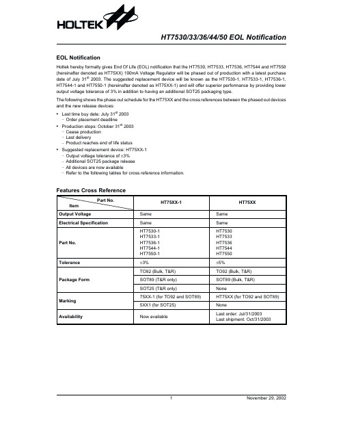
Production stops After this specified date no more devices will be manufactured and last deliveries made. At this point the device can be said to have reached their end of life status.
H T75X X
. ro n t V ie w
V O U T G N D V IN
B o tto m V ie w
HT75XX Output Voltage
3.0V±5% 3.3V±5% 3.6V±5% 4.4V±5% 5.0V±5%
Order No./ Marking
HT7530 HT7533 HT7536 HT7544 HT7550
HT7530/33/36/44/50 EOL Notification
EOL Notification
Holtek hereby formally gives End Of Life (EOL) notification that the HT7530, HT7533, HT7536, HT7544 and HT7550 (hereinafter denoted as HT75XX) 100mA Voltage Regulator will be phased out of production with a latest purchase date of July 31st 2003. The suggested replacement device will be known as the HT7530-1, HT7533-1, HT7536-1, HT7544-1 and HT7550-1 (hereinafter denoted as HT75XX-1) and will offer superior performance by providing lower output voltage tolerance of 3% in addition to having an additional SOT25 packaging type.
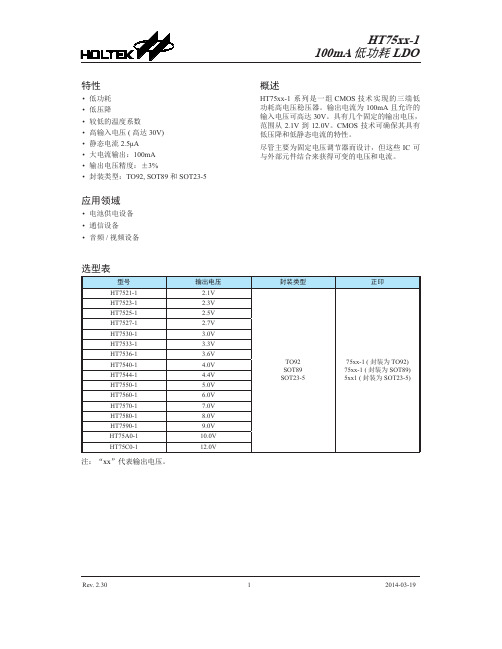
HT7533,HT7550芯片特征和应用范围
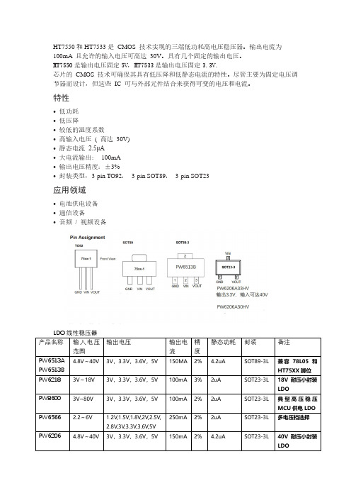
HT7550和HT7533是CMOS 技术实现的三端低功耗高电压稳压器。
输出电流为100mA 且允许的输入电压可高达30V。
具有几个固定的输出电压。
HT7550是输出电压固定5V,HT7533是输出电压固定3.3V.芯片的CMOS 技术可确保其具有低压降和低静态电流的特性。
尽管主要为固定电压调节器而设计,但这些IC 可与外部元件结合来获得可变的电压和电流。
特性• 低功耗• 低压降• 较低的温度系数• 高输入电压( 高达30V)• 静态电流2.5μA• 大电流输出:100mA• 输出电压精度:±3%• 封装类型:3-pin TO92,3-pin SOT89,3-pin SOT23应用领域• 电池供电设备• 通信设备• 音频/ 视频设备PW6206GENERAL DESCRIPTIONThe PW6206 series is a high accuracy, high input voltage low quiescent current, high speed, and low dropout liner regulator with high ripple rejection. The input voltage is up to 40V and load current is up to 300mA at VOUT = 5V & VIN = 7V. The device is manufactured with BCD process. The PW6206 offers over-current limit, soft start and over temperature protection to ensure the device working in well conditionsFEATURES● Input voltage: 4.75V~40V ● Output voltage: 1.8V~5.7V ● Output accuracy: < ±2%● Output current: 150mA (Typ.)● Up to 300mA @ VIN = 7V, VOUT = 5V, PW6206B50HV package ● PSRR: 60dB @ 100Hz● Dropout voltage: 600mV @ IOUT = 100mA ● Quiescent current: 4.2μA @ VIN = 12V(Typ.) ● ESD HBM: 8KV●Recommend capacitor: 10μFAPPLICATIONS● Smart electric meter ● In-car entertainment ● Electric bicycleTYPICAL APPLICATION CIRCUIT123SOT23-3VOUTGND VIN在输入串联一个2R的电阻,可以吸收拔插尖峰浪涌PW6513GENERAL DESCRIPTIONThe PW6513 series is a high accuracy, high input voltage low quiescent current, high speed, and low dropout liner regulator with high ripple rejection. The input voltage is up to 40V and load current is up to 300mA at VOUT = 5V & VIN = 7V. The device is manufactured with BCD process. The PW6513 offers over-current limit, soft start and over temperature protection to ensure the device working in well conditionsThe PW6513 regulators is available in standard SOT89-3L packages. Standard products are Pb-free and Halogen-free.FEATURES⚫ Input voltage: 4.75V~40V ⚫ Output voltage: 1.8V~5.7V ⚫ Output accuracy: < ±2%⚫ Output current: 150mA (Typ.)⚫ Up to 300mA @ VIN = 7V, VOUT = 5V, ⚫ PSRR: 60dB @ 100Hz⚫ Dropout voltage: 600mV @ IOUT = 100mA ⚫ Quiescent current: 4.2μA @ VIN = 12V(Typ.) ⚫ ESD HBM: 8KV⚫Recommend capacitor: 10μFAPPLICATIONS⚫ Smart electric meter⚫ In-car entertainment ⚫ Electric bicycleTYPICAL APPLICATION CIRCUITPW6513APW6513B。
HOLTEK_HT7533参数资料

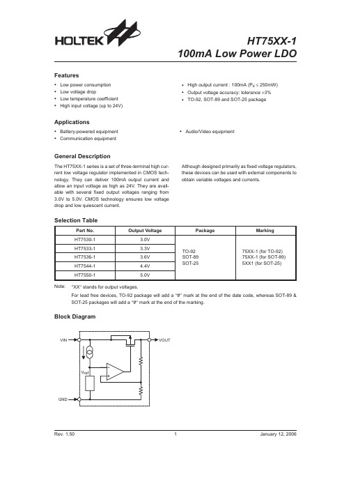
HT75XX-1100mA Low Power LDOSelection TablePart No.Output VoltagePackageMarkingHT7530-1 3.0V TO-92SOT-89SOT-2575XX-1(for TO-92)75XX-1(for SOT-89)5XX1(for SOT-25)HT7533-1 3.3V HT7536-1 3.6V HT7544-1 4.4V HT7550-15.0VNote:²XX ²stands for output voltages.For lead free devices,TO-92package will add a ²#²mark at the end of the date code,whereas SOT-89&SOT-25packages will add a ²#²mark at the end of the marking.Block DiagramRev.1.501January 12,2006Features·Low power consumption ·Low voltage drop·Low temperature coefficient ·High input voltage (up to 24V)·High output current :100mA (P d £250mW)·Output voltage accuracy:tolerance ±3%·TO-92,SOT-89and SOT-25packageApplications·Battery-powered equipment ·Communication equipment·Audio/Video equipmentGeneral DescriptionThe HT75XX-1series is a set of three-terminal high cur-rent low voltage regulator implemented in CMOS tech-nology.They can deliver 100mA output current and allow an input voltage as high as 24V.They are avail-able with several fixed output voltages ranging from 3.0V to 5.0V.CMOS technology ensures low voltage drop and low quiescent current.Although designed primarily as fixed voltage regulators,these devices can be used with external componentsto obtain variable voltages andcurrents.Pin AssignmentAbsolute Maximum RatingsSupply Voltage..........................................-0.3V to26V Storage Temperature............................-50°C to125°C Power Consumption(*1)..................................250mW Operating Temperature...........................-40°C to85°C Power Consumption(*2)..................................150mWNote:These are stress ratings only.Stresses exceeding the range specified under²Absolute Maximum Ratings²may cause substantial damage to the device.Functional operation of this device at other conditions beyond those listed in the specification is not implied and prolonged exposure to extreme conditions may affect device reliabil-ity.*1:applied to SOT89and TO-92*2:applied to SOT-25Electrical CharacteristicsHT7530-1,+3.0V Output Type Ta=25°CSymbol ParameterTest ConditionsMin.Typ.Max.Unit V IN ConditionsV OUT Output Voltage Tolerance5V I OUT=10mA 2.91 3.0 3.09V I OUT Output Current5V¾60100¾mA D V OUT Load Regulation5V1mA£I OUT£50mA60150mV V DIF Voltage Drop¾I OUT=1mA¾100¾mV I SS Current Consumption5V No load¾ 2.55m ALine Regulation¾4V£V IN£24VI OUT=1mA¾0.2¾%/VV IN Input Voltage¾¾¾¾24VTemperature Coefficient5V I OUT=10mA0°C<Ta<70°C¾±0.45¾mV/°CRev.1.502January12,2006Symbol ParameterTest ConditionsMin.Typ.Max.Unit V IN ConditionsV OUT Output Voltage Tolerance 5.5V I OUT=10mA 3.201 3.3 3.399V I OUT Output Current 5.5V¾60100¾mA D V OUT Load Regulation 5.5V1mA£I OUT£50mA¾60150mV V DIF Voltage Drop¾I OUT=1mA¾100¾mV I SS Current Consumption 5.5V No load¾ 2.55m ALine Regulation¾4.5V£V IN£24VI OUT=1mA¾0.2¾%/VV IN Input Voltage¾¾¾¾24VTemperature Coefficient 5.5V I OUT=10mA0°C<Ta<70°C¾±0.5¾mV/°CHT7536-1,+3.6V Output Type Ta=25°CSymbol ParameterTest ConditionsMin.Typ.Max.Unit V IN ConditionsV OUT Output Voltage Tolerance 5.6V I OUT=10mA 3.492 3.6 3.708V I OUT Output Current 5.6V¾60100¾mA D V OUT Load Regulation 5.6V1mA£I OUT£50mA¾60150mV V DIF Voltage Drop¾I OUT=1mA¾100¾mV I SS Current Consumption 5.6V No load¾ 2.55m ALine Regulation¾4.6V£V IN£24VI OUT=1mA¾0.2¾%/VV IN Input Voltage¾¾¾¾24VTemperature Coefficient 5.6V I OUT=10mA0°C<Ta<70°C¾±0.6¾mV/°CHT7544-1,+4.4V Output Type Ta=25°CSymbol ParameterTest ConditionsMin.Typ.Max.Unit V IN ConditionsV OUT Output Voltage Tolerance 6.4V I OUT=10mA 4.268 4.4 4.532V I OUT Output Current 6.4V¾60100¾mA D V OUT Load Regulation 6.4V1mA£I OUT£50mA¾60150mV V DIF Voltage Drop¾I OUT=1mA¾100¾mV I SS Current Consumption 6.4V No load¾ 2.55m ALine Regulation¾5.4V£V IN£24VI OUT=1mA¾0.2¾%/VV IN Input Voltage¾¾¾¾24VTemperature Coefficient 6.4V I OUT=10mA0°C<Ta<70°C¾±0.7¾mV/°CRev.1.503January12,2006Symbol ParameterTest ConditionsMin.Typ.Max.Unit V IN ConditionsV OUT Output Voltage Tolerance7V I OUT=10mA 4.85 5.0 5.15V I OUT Output Current7V¾100150¾mA D V OUT Load Regulation7V1mA£I OUT£70mA¾60150mV V DIF Voltage Drop¾I OUT=1mA¾100¾mV I SS Current Consumption7V No load¾ 2.55m ALine Regulation¾6V£V IN£24VI OUT=1mA¾0.2¾%/VV IN Input Voltage¾¾¾¾24VTemperature Coefficient7V I OUT=10mA0°C<Ta<70°C¾±0.75¾mV/°CApplication CircuitsBasic CircuitHigh Output Current Positive Voltage RegulatorRev.1.504January12,2006Short-Circuit Protection for Tr1Circuit for Increasing Output VoltageV=V(1+R2R1)+I R2OUT XX SSCircuit for Increasing Output VoltageV=V+VOUT XX D1Rev.1.505January12,2006Constant Current RegulatorI=VR+IOUTXXASSDual SupplyRev.1.506January12,2006Package Information3-pin TO-92Outline DimensionsSymbolDimensions in milMin.Nom.Max.A170¾200B170¾200C500¾¾D11¾20E90¾110F45¾55G45¾65H130¾160I8¾18a4°¾6°Rev.1.507January12,2006SymbolDimensions in milMin.Nom.Max.A173¾181B64¾72C90¾102D35¾47E155¾167F14¾19G17¾22H¾59¾I55¾63J14¾17Rev.1.508January12,2006SymbolDimensions in mmMin.Nom.Max.A 1.00¾ 1.30A1¾¾0.10A20.70¾0.90b0.35¾0.50C0.10¾0.25D 2.70¾ 3.10E 1.40¾ 1.80e¾ 1.90¾H 2.60¾3L0.37¾¾q1°¾9°Rev.1.509January12,2006Product Tape and Reel SpecificationsTO-92Reel Dimensions(Unit:mm)Rev.1.5010January12,2006SOT-89&SOT-25Reel DimensionsSOT-89Symbol Description Dimensions in mmA Reel Outer Diameter180±1.0B Reel Inner Diameter62±1.5C Spindle Hole Diameter12.75+0.15D Key Slit Width 1.9±0.15T1Space Between Flange12.4+0.2T2Reel Thickness17-0.4SOT-25Symbol Description Dimensions in mmA Reel Outer Diameter178±1.0B Reel Inner Diameter62±1.0C Spindle Hole Diameter13.0±0.2D Key Slit Width 2.5±0.25T1Space Between Flange 8.4+1.5-0.0T2Reel Thickness11.4+1.5Rev.1.5011January12,2006TO-92Carrier Tape DimensionsTO-92Symbol Description Dimensions in mm I1Taped Lead Length(2.5)P Component Pitch12.7±1.0P0Perforation Pitch12.7±0.3P2Component to Perforation(Length Direction) 6.35±0.4F1Lead Spread 2.5+0.4-0.1F2Lead Spread 2.5+0.4-0.1D h Component Alignment0±0.1W Carrier Tape Width 18.0+1.0-0.5W0Hold-down Tape Width 6.0±0.5W1Perforation Position9.0±0.5W2Hold-down Tape Position(0.5)H0Lead Clinch Height16.0±0.5H1Component Height Less than24.7D0Perforation Diameter 4.0±0.2t Taped Lead Thickness0.7±0.2H Component Base Height19.0±0.5Note:Thickness less than0.38±0.05mm~0.5mmP0Accumulated pitch tolerance:±1mm/20pitches.()Bracketed figures are for consultation onlyRev.1.5012January12,2006SOT-89&SOT-25Carrier Tape DimensionsSOT-89Symbol Description Dimensions in mmW Carrier Tape Width 12.0+0.3-0.1P Cavity Pitch8.0±0.1E Perforation Position 1.75±0.1F Cavity to Perforation(Width Direction) 5.5±0.05D Perforation Diameter 1.5+0.1D1Cavity Hole Diameter 1.5+0.1P0Perforation Pitch 4.0±0.1P1Cavity to Perforation(Length Direction) 2.0±0.10A0Cavity Length 4.8±0.1B0Cavity Width 4.5±0.1K0Cavity Depth 1.8±0.1t Carrier Tape Thickness0.30±0.013C Cover Tape Width9.3SOT-25Symbol Description Dimensions in mm W Carrier Tape Width8.0±0.3P Cavity Pitch 4.0E Perforation Position 1.75F Cavity to Perforation(Width Direction) 3.5±0.05D Perforation Diameter 1.5+0.1D1Cavity Hole Diameter 1.5+0.1P0Perforation Pitch 4.0P1Cavity to Perforation(Length Direction) 2.0A0Cavity Length 3.15B0Cavity Width 3.2K0Cavity Depth 1.4t Carrier Tape Thickness0.20±0.03C Cover Tape Width 5.3Rev.1.5013January12,2006Holtek Semiconductor Inc.(Headquarters)No.3,Creation Rd.II,Science Park,Hsinchu,TaiwanTel:886-3-563-1999Fax:886-3-563-1189Holtek Semiconductor Inc.(Taipei Sales Office)4F-2,No.3-2,YuanQu St.,Nankang Software Park,Taipei115,TaiwanTel:886-2-2655-7070Fax:886-2-2655-7373Fax:886-2-2655-7383(International sales hotline)Holtek Semiconductor Inc.(Shanghai Sales Office)7th Floor,Building2,No.889,Yi Shan Rd.,Shanghai,China200233Tel:021-6485-5560Fax:021-6485-0313Holtek Semiconductor Inc.(Shenzhen Sales Office)43F,SEG Plaza,Shen Nan Zhong Road,Shenzhen,China518031Tel:0755-8346-5589Fax:0755-8346-5590ISDN:0755-8346-5591Holtek Semiconductor Inc.(Beijing Sales Office)Suite1721,Jinyu Tower,A129West Xuan Wu Men Street,Xicheng District,Beijing,China100031Tel:010-6641-0030,6641-7751,6641-7752Fax:010-6641-0125Holmate Semiconductor,Inc.(North America Sales Office)46712Fremont Blvd.,Fremont,CA94538Tel:510-252-9880Fax:510-252-9885CopyrightÓ2006by HOLTEK SEMICONDUCTOR INC.The information appearing in this Data Sheet is believed to be accurate at the time of publication.However,Holtek as-sumes no responsibility arising from the use of the specifications described.The applications mentioned herein are used solely for the purpose of illustration and Holtek makes no warranty or representation that such applications will be suitable without further modification,nor recommends the use of its products for application that may present a risk to human life due to malfunction or otherwise.Holtek¢s products are not authorized for use as critical components in life support devices or systems.Holtek reserves the right to alter its products without prior notification.For the most up-to-date information, please visit our web site at .Rev.1.5014January12,2006This datasheet has been downloaded from:Free DownloadDaily Updated Database100% Free Datasheet Search Site100% Free IC Replacement Search SiteConvenient Electronic DictionaryFast Search SystemAll Datasheets Cannot Be Modified Without PermissionCopyright © Each Manufacturing Company。
HT7536中文资料

HT75XXHigh Driver RegulatorSelection TablePart No.Output VoltageToleranceHT7530 3.0V ±5%HT7533 3.3V ±5%HT7536 3.6V ±5%HT7544 4.4V ±5%HT7550 5.0V ±5%HT75808.0V±5%1May 2,2000Features·Low power consumption ·Low voltage drop·Low temperature coefficient ·High input voltage (up to 24V)·High output current :100mA (P d £250mW)·TO-92and SOT-89packageApplications·Battery-powered equipment ·Communication equipment·Audio/Video equipmentGeneral DescriptionThe HT75XX series is a set of three-terminal high current low voltage regulator imple-mented in CMOS technology.They can deliver 100mA output current and allow an input volt-age as high as 24V .They are available with sev-eral fixed output voltages ranging from 3.0V to 8V .CMOS technology ensures low voltage drop and low quiescent current.Although designed primarily as fixed voltage regulators,these devices can be used with ex-ternal components to obtain variable voltages and currents.Block DiagramPin AssignmentHT75XX2May 2,2000Pad Assignment Pad Coordinates Unit:m mPad No.X Y1-506.50-589.50261.00-582.503510.50-585.50 Chip size:1390´1530(m m)2*The IC substrate should be connected to VDD in the PCB layout artwork.Absolute Maximum RatingsSupply Voltage...............................-0.3V to26V Storage Temperature.................-50°C to125°C Power Consumption..............................250mW Operating Temperature..................0°C to70°CNote:These are stress ratings only.Stresses exceeding the range specified under²Absolute Maxi-mum Ratings²may cause substantial damage to the device.Functional operation of this device at other conditions beyond those listed in the specification is not implied and prolonged expo-sure to extreme conditions may affect device reliability.3May2,2000Electrical CharacteristicsHT7530,+3.0V output type Ta=25°CHT7533,+3.3V output type Ta=25°C4May2,2000HT7544,+4.4V output type Ta=25°C5May2,2000HT7580,+8.0V output type Ta=25°C6May2,2000Application CircuitsBasic circuitHigh output current positive voltage regulatorShort-Circuit protection for Tr1HT75XX7May 2,2000Circuit for increasing output voltageV=V(1+R2R1)+I R2OUT XX SS Circuit for increasing output voltageV=V+VOUT XX D1 Constant current regulatorI=VR +IOUTXXASS8May2,2000Dual supply9May2,200010May 2,2000Copyright ã2000by HOLTEK SEMICONDUCTOR INC.The information appearing in this Data Sheet is believed to be accurate at the time of publication.However,Holtek assumes no responsibility arising from the use of the specifications described.The applications mentioned herein are used solely for the purpose of illustration and Holtek makes no warranty or representation that such applications will be suitable without further modification,nor recommends the use of its products for application that may pres-ent a risk to human life due to malfunction or otherwise.Holtek reserves the right to alter its products without prior notification.For the most up-to-date information,please visit our web site at .Holtek Semiconductor Inc.(Headquarters)No.3Creation Rd.II,Science-based Industrial Park,Hsinchu,Taiwan,R.O.C.Tel:886-3-563-1999Fax:886-3-563-1189Holtek Semiconductor Inc.(Taipei Office)5F,No.576,Sec.7Chung Hsiao E.Rd.,Taipei,Taiwan,R.O.C.Tel:886-2-2782-9635Fax:886-2-2782-9636Fax:886-2-2782-7128(International sales hotline)Holtek Semiconductor (Hong Kong)Ltd.RM.711,Tower 2,Cheung Sha Wan Plaza,833Cheung Sha Wan Rd.,Kowloon,Hong Kong Tel:852-2-745-8288Fax:852-2-742-8657。
封装参考
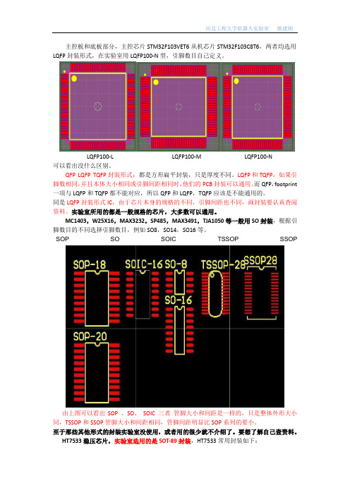
主控板和底板部分,主控芯片STM32F103VET6从机芯片STM32F103C8T6,两者均选用LQFP封装形式,在实验室用LQFP100-N型,引脚数目自己定义。
LQFP100-L LQFP100-M LQFP100-N可以看出没什么区别。
QFP LQFP TQFP封装形式:都是方形扁平封装,只是厚度不同。
LQFP和TQFP,如果引脚数相同,并且本体大小相同或引脚间距相同时,他们的PCB封装可以通用。
而QFP,footprint 一项与LQFP和TQFP都不能对应,所以QFP和LQFP,TQFP应该是不能通用的。
同是LQFP封装形式IC,由于芯片本身的规格的不同,引脚间距也不同,画封装要认真查阅资料。
实验室所用的都是一般规格的芯片,大多数可以通用。
MC1403,W25X16,MAX3232,SP485,MAX3491,TJA1050等一般用SO封装,根据引脚数目的不同选择引脚数目,例如SO8,SO14,SO16等。
SOP SO SOIC TSSOP SSOP由上图可以看出SOP 、SO、SOIC 三者管脚大小和间距是一样的,只是整体外形大小同,TSSOP和SSOP管脚大小和间距相同,管脚间距明显比SOP系列的要小。
至于那些其他形式的封装实验室没使用,或者用的很少就不介绍了。
要想了解自己查资料。
HT7533稳压芯片,实验室选用的是SOT-89封装,HT7533常用封装如下:SOT-89SOT-25TO-92二极管的一般封装:DO-35,DO-41玻封二极管;LL-34,LL-41玻封二极管;DO-41塑封二极管;SOD123,SOD323,SOD523塑封二极管;TO220封装。
SOT23贴片二极管。
DO-35 DO-41LL-34 LL-41DO-41 SOD123,SOD323,SOD523TO220 SOT23其对应的封装形式:TO220 DO-41DO-35 SOT23LL-34 LL-41 对应为1206贴片封装;SOD123对应为1206,SOD323对应为0805,SOD523对应为0603,一般的LED发光二极管用0805封装。
HT75XX HT7533 有技术支持

4.300
4.700
e
1.270 TYP
e1
2.440
2.640
L
14.100
14.500
Φ
h
0.000
2、SOT-89-3
1.600 0.380
HT75XX 系列 (Ver 1.10) 曾先生:13534002546
符号 A b b1 c D D1 E E1 e e1 L
最小值(mm)
最大值(mm)
HT75XX 系列 (Ver 1.10)
HT75××系列 线性稳压器
曾先生:13534002546
产品概括
特点
HT75XX 系列是采用 CMOS 工艺制造, 低功耗的高压稳压器,最高输入电压可 达 12V,输出电压范围为 2.0V~5.0V。 它具有高精度的输出电压、极低的供电 电流、极低的跌落电压等特点。
-
%/V
-
-
-
+0.75
10
V
-
mV/℃
应用电路
1、基本电路
2、高输出电流稳压电路
3、短路保护电路
4(8)
4、提高输出电压电路
HT75XX 系列 (Ver 1.10) 曾先生:13534002546
VOUT=Vxx(1+R2/R1)+Iss*R2
5、电流调节电路
VOUT=Vxx+VD1
IOUT = VXX/RX + ISS
△VOUT
输出电压 输出电流 负载调节
测试条件
VIN=7V,IOUT=1mA VIN=7V
VIN=7V,1mA≤IOUT≤ 30mA
最小值 4.85 60 -
TOPT=25℃ 典型值 最大值
HT7533datasheet
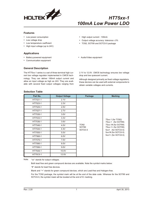
HT75xx-1100mA Low Power LDOSelection TableNote:²xx ²stands for output voltages.Both lead free and green compound devices are available.Note the symbol marks below:²#²stands for lead free devices.Blank and ²+²stands for green compound devices,which are Lead-free and Halogen-free.For the TO92package,the symbol mark will be at the end of the date code.Whereas for the SOT89and SOT23-5,the symbol mask will be located at the end of IC marking.Rev.2.201April 30,2013Features·Low power consumption ·Low voltage drop·Low temperature coefficient ·High input voltage (up to 24V)·High output current :100mA·Output voltage accuracy:tolerance ±3%·TO92,SOT89and SOT23-5packageApplications·Battery-powered equipment ·Communication equipment·Audio/Video equipmentGeneral DescriptionThe HT75xx-1series is a set of three-terminal high cur-rent low voltage regulator implemented in CMOStech-nology.They can deliver 100mA output current and allow an input voltage as high as 24V.They are avail-able with several fixed output voltages ranging from2.1V to 12.0V.CMOS technology ensures low voltage drop and low quiescent current.Although designed primarily as fixed voltage regulators,these devices can be used with external components to obtain variable voltages and currents.Block DiagramPin AssignmentAbsolute Maximum RatingsSupply Voltage .........................................-0.3V to 26V Storage Temperature ...........................-50°C to 125°COperating Temperature ..........................-40°C to 85°CNote:These are stress ratings only.Stresses exceeding the range specified under ²Absolute Maximum Ratings ²maycause substantial damage to the device.Functional operation of this device at other conditions beyond those listed in the specification is not implied and prolonged exposure to extreme conditions may affect device reliability.Thermal InformationNote:P D is measured atTa=25°C HT75xx-1Rev.2.202April 30,2013Electrical CharacteristicsHT7521-1, +2.1V Output Type Ta=25°CNote:Dropout voltage is defined as the input voltage minus the output voltage that produces a 2% change in the output voltage from the value at V IN=V OUT+2V with a fixed load.HT7523-1, +2.3V Output Type Ta=25°CNote:Dropout voltage is defined as the input voltage minus the output voltage that produces a 2% change in the output voltage from the value at V IN=V OUT+2V with a fixed load.Rev. 2.203April 30, 2013Note:Dropout voltage is defined as the input voltage minus the output voltage that produces a 2% change in the output voltage from the value at V IN=V OUT+2V with a fixed load.HT7527-1, +2.7V Output Type Ta=25°CNote:Dropout voltage is defined as the input voltage minus the output voltage that produces a 2% change in the output voltage from the value at V IN=V OUT+2V with a fixed load.Rev. 2.204April 30, 2013Note:Dropout voltage is defined as the input voltage minus the output voltage that produces a 2% change in the output voltage from the value at V IN=V OUT+2V with a fixed load.HT7533-1, +3.3V Output Type Ta=25°CNote:Dropout voltage is defined as the input voltage minus the output voltage that produces a 2% change in the output voltage from the value at V IN=V OUT+2V with a fixed load.Rev. 2.205April 30, 2013Note:Dropout voltage is defined as the input voltage minus the output voltage that produces a 2% change in the output voltage from the value at V IN=V OUT+2V with a fixed load.HT7540-1, +4.0V Output Type Ta=25°CNote:Dropout voltage is defined as the input voltage minus the output voltage that produces a 2% change in the output voltage from the value at V IN=V OUT+2V with a fixed load.Rev. 2.206April 30, 2013Note:Dropout voltage is defined as the input voltage minus the output voltage that produces a 2% change in the output voltage from the value at V IN=V OUT+2V with a fixed load.HT7550-1, +5.0V Output Type Ta=25°CNote:Dropout voltage is defined as the input voltage minus the output voltage that produces a 2% change in the output voltage from the value at V IN=V OUT+2V with a fixed load.Rev. 2.207April 30, 2013Note:Dropout voltage is defined as the input voltage minus the output voltage that produces a 2% change in the output voltage from the value at V IN=V OUT+2V with a fixed load.HT7570-1, +7.0V Output Type Ta=25°CNote:Dropout voltage is defined as the input voltage minus the output voltage that produces a 2% change in the output voltage from the value at V IN=V OUT+2V with a fixed load.Rev. 2.208April 30, 2013Note:Dropout voltage is defined as the input voltage minus the output voltage that produces a 2% change in the output voltage from the value at V IN=V OUT+2V with a fixed load.HT7590-1, +9.0V Output Type Ta=25°CNote:Dropout voltage is defined as the input voltage minus the output voltage that produces a 2% change in the output voltage from the value at V IN=V OUT+2V with a fixed load.Rev. 2.209April 30, 2013Note:Dropout voltage is defined as the input voltage minus the output voltage that produces a 2% change in the output voltage from the value at V IN=V OUT+2V with a fixed load.HT75C0-1, +12.0V Output Type Ta=25°CNote:Dropout voltage is defined as the input voltage minus the output voltage that produces a 2% change in the output voltage from the value at V IN=V OUT+2V with a fixed load.Rev. 2.2010April 30, 2013Typical Performance CharacteristicsRev. 2.2011April 30, 2013Rev. 2.2012April 30, 2013Rev. 2.2013April 30, 2013Application CircuitsBasic CircuitHigh Output Current Positive Voltage RegulatorShort-Circuit Protection for Tr1Rev.2.2014April30,2013Circuit for Increasing Output VoltageV=V(1+R2R1)+I R2OUT XX SS Circuit for Increasing Output VoltageV=V+VOUT XX D1 Constant Current RegulatorI=VR+IOUTXXASSDual SupplyRev.2.2015April30,2013Package InformationNote that the package information provided here is for consultation purposes only.As this information may be updated at regular intervals users are reminded to consult the Holtek website for the latest version of the package information.Additional supplementary information with regard to packaging is listed below.Click on the relevant section to be transferred to the relevant website page.·Further Package Information(include Outline Dimensions,Product Tape and Reel Specifications)·Packing Meterials Information·Carton information·PB FREE Products·Green Packages ProductsRev.2.2016April30,2013Rev.2.2017April30,2013Rev.2.2018April30,2013Rev.2.2019April30,2013CopyrightÓ2013by HOLTEK SEMICONDUCTOR INC.The information appearing in this Data Sheet is believed to be accurate at the time of publication. However,Holtek assumes no responsibility arising from the use of the specifications described. The applications mentioned herein are used solely for the purpose of illustration and Holtek makes no warranty or representation that such applications will be suitable without further modi-fication,nor recommends the use of its products for application that may present a risk to human life due to malfunction or otherwise.Holtek¢s products are not authorized for use as critical com-ponents in life support devices or systems.Holtek reserves the right to alter its products without prior notification.For the most up-to-date information,please visit our web site at .Rev.2.2020April30,2013。
AD7533JN中文资料
Operating Conditions
Temperature Range . . . . . . . . . . . . . . . . . . . . . . . . . . . . 0oC to 70oC
CAUTION: Stresses above those listed in “Absolute Maximum Ratings” may cause permanent damage to the device. This is a stress only rating and operation of the device at these or any other conditions above those indicated in the operational sections of this specification is not implied.
2
元器件交易网
AD7533
Electrical Specifications
V+ = +15V, VREF = +10V, VOUT1 = VOUT2 = 0V, Unless Otherwise Specified (Continued) TA 25oC PARAMETER ANALOG OUTPUT Output Capacitance COUT1 All Digital Inputs High (Note 4) COUT2 COUT1 All Digital Inputs Low (Note 4) COUT2 DIGITAL INPUTS Low State Threshold, VIL High State Threshold, VIH Input Current (Low or High), IIL, IIH Input Coding Input Capacitance VIN = 0V or + 15V See Tables 1 through 3 (Note 4) 2.4 0.8 ±1 2.4 0.8 ±1 V V µA 100 35 35 100 100 35 35 100 pF pF pF pF TEST CONDITIONS MIN MAX TA MIN-MAX MIN MAX UNITS
宽电压稳压IC方案HT7533

Rev. 1.5012014-03-19• 低压降• 较低的温度系数• 高输入电压 (高达 30V)• 静态电流 2.5μA • 大电流输出:100m A • 输出电压精度:±1%• 封装类型:TO92, SOT89 和 SOT23-5应用领域• 电池供电设备• 通信设备• 音频/视频设备HT75xx-2 系列是一组CMOS 技术实现的三端低功耗高电压稳压器。
输出电流为 100m A 且允许的输入电压可高达 30V 。
具有几个固定的输出电压,范围从 2.1V 到 12.0V 。
CMOS 技术可确保其具有低压降和低静态电流的特性。
尽管主要为固定电压调节器而设计,但这些 IC 可与外部元件结合来获得可变的电压和电流。
选型表注:“xx ”代表输出电压。
Rev. 1.5022014-03-19引脚图nt极限参数电源供应电压 ...................................................−0.3V ~ 33V 储存温度范围 ...............................................−50°C ~ 125°C工作环境温度 .................................................−40°C ~ 85°C注: 这里只强调额定功率,超过极限参数所规定的范围将对芯片造成损害,无法预期芯片在上述标示范围外的工作状态,而且若长期在标示范围外的条件下工作,可能影响芯片的可靠性。
热能信息注:P D 值是在 Ta = 25°C 时测得。
电气特性HT7521-2, +2.1V 输出类型注:在 V IN = V OUT+2V 与一个固定负载条件下使输出电压下降 2%,此时的输入电压减去输出电压就是Dropout 电压。
HT7523-2, +2.3V 输出类型注:在 V IN = V OUT+2V 与一个固定负载条件下使输出电压下降 2%,此时的输入电压减去输出电压就是Dropout 电压。
HT 规格书
•低压降•较低的温度系数•高输入电压 (高达 30V)•静态电流 2.5μA•大电流输出:100mA•输出电压精度:±3%•封装类型:TO92, SOT89 和 SOT23-5应用领域•电池供电设备•通信设备•音频/视频设备功耗高电压稳压器。
输出电流为 100mA 且允许的输入电压可高达 30V。
具有几个固定的输出电压,范围从 2.1V 到 12.0V。
CMOS 技术可确保其具有低压降和低静态电流的特性。
尽管主要为固定电压调节器而设计,但这些 IC 可与外部元件结合来获得可变的电压和电流。
注:“xx”代表输出电压。
Rev. 2.3012014-03-19引脚图极限参数工作环境温度 .................................................−40°C ~ 85°C 电源供应电压 ...................................................−0.3V ~ 33V储存温度范围 ...............................................−50°C ~ 125°C注:这里只强调额定功率,超过极限参数所规定的范围将对芯片造成损害,无法预期芯片在上述标示范围外的工作状态,而且若长期在标示范围外的条件下工作,可能影响芯片的可靠性。
热能信息Rev. 2.3022014-03-19电气特性HT7521-1, +2.1V 输出类型注:在 V IN = V OUT+2V 与一个固定负载条件下使输出电压下降 2%,此时的输入电压减去输出电压就是Dropout 电压。
HT7523-1, +2.3V 输出类型注:在 V IN = V OUT+2V 与一个固定负载条件下使输出电压下降 2%,此时的输入电压减去输出电压就是Dropout 电压。
Rev. 2.3032014-03-19注:在 V IN = V OUT+2V 与一个固定负载条件下使输出电压下降 2%,此时的输入电压减去输出电压就是Dropout 电压。
宽电压稳压IC方案HT7533
Rev. 1.5012014-03-19• 低压降• 较低的温度系数• 高输入电压 (高达 30V)• 静态电流 2.5μA • 大电流输出:100m A • 输出电压精度:±1%• 封装类型:TO92, SOT89 和 SOT23-5应用领域• 电池供电设备• 通信设备• 音频/视频设备HT75xx-2 系列是一组CMOS 技术实现的三端低功耗高电压稳压器。
输出电流为 100m A 且允许的输入电压可高达 30V 。
具有几个固定的输出电压,范围从 2.1V 到 12.0V 。
CMOS 技术可确保其具有低压降和低静态电流的特性。
尽管主要为固定电压调节器而设计,但这些 IC 可与外部元件结合来获得可变的电压和电流。
选型表注:“xx ”代表输出电压。
Rev. 1.5022014-03-19引脚图nt极限参数电源供应电压 ...................................................−0.3V ~ 33V 储存温度范围 ...............................................−50°C ~ 125°C工作环境温度 .................................................−40°C ~ 85°C注: 这里只强调额定功率,超过极限参数所规定的范围将对芯片造成损害,无法预期芯片在上述标示范围外的工作状态,而且若长期在标示范围外的条件下工作,可能影响芯片的可靠性。
热能信息注:P D 值是在 Ta = 25°C 时测得。
电气特性HT7521-2, +2.1V 输出类型注:在 V IN = V OUT+2V 与一个固定负载条件下使输出电压下降 2%,此时的输入电压减去输出电压就是Dropout 电压。
HT7523-2, +2.3V 输出类型注:在 V IN = V OUT+2V 与一个固定负载条件下使输出电压下降 2%,此时的输入电压减去输出电压就是Dropout 电压。
封装参考

封装参考————————————————————————————————作者:————————————————————————————————日期:主控板和底板部分,主控芯片STM32F103VET6从机芯片STM32F103C8T6,两者均选用LQFP封装形式,在实验室用LQFP100-N型,引脚数目自己定义。
LQFP100-L LQFP100-M LQ FP100-N可以看出没什么区别。
QFPLQFP TQFP封装形式:都是方形扁平封装,只是厚度不同。
LQFP和TQFP,如果引脚数相同,并且本体大小相同或引脚间距相同时,他们的PCB封装可以通用。
而QFP,foo tprint一项与LQFP和TQFP都不能对应,所以QFP和LQFP,TQFP应该是不能通用的。
同是LQFP封装形式IC,由于芯片本身的规格的不同,引脚间距也不同,画封装要认真查阅资料。
实验室所用的都是一般规格的芯片,大多数可以通用。
MC1403,W25X16,MAX3232,SP485,MAX3491,TJA1050等一般用SO封装,根据引脚数目的不同选择引脚数目,例如SO8,SO14,SO16等。
SOP SOSOIC TSSOP SSOP由上图可以看出SOP、SO、SOIC 三者管脚大小和间距是一样的,只是整体外形大小同,TSSOP和SSOP管脚大小和间距相同,管脚间距明显比SOP系列的要小。
至于那些其他形式的封装实验室没使用,或者用的很少就不介绍了。
要想了解自己查资料。
HT7533稳压芯片,实验室选用的是SOT-89封装,HT7533常用封装如下:SOT-89SOT-25TO-92二极管的一般封装:DO-35,DO-41玻封二极管;LL-34,LL-41玻封二极管;DO-41塑封二极管;SOD123,SOD323,SOD523塑封二极管;TO220封装。
SOT23贴片二极管。
DO-35DO-41LL-34LL-41DO-41 SOD123,SOD323,SOD523TO220SOT23其对应的封装形式:TO220DO-41DO-35SOT23LL-34LL-41对应为1206贴片封装;SOD123对应为1206,SOD323对应为0805,S OD523对应为0603,一般的LED发光二极管用0805封装。
HT7530中文资料
HT75XXHigh Driver RegulatorSelection TablePart No.Output VoltageToleranceHT7530 3.0V ±5%HT7533 3.3V ±5%HT7536 3.6V ±5%HT7544 4.4V ±5%HT7550 5.0V ±5%HT75808.0V±5%1May 2,2000Features·Low power consumption ·Low voltage drop·Low temperature coefficient ·High input voltage (up to 24V)·High output current :100mA (P d £250mW)·TO-92and SOT-89packageApplications·Battery-powered equipment ·Communication equipment·Audio/Video equipmentGeneral DescriptionThe HT75XX series is a set of three-terminal high current low voltage regulator imple-mented in CMOS technology.They can deliver 100mA output current and allow an input volt-age as high as 24V .They are available with sev-eral fixed output voltages ranging from 3.0V to 8V .CMOS technology ensures low voltage drop and low quiescent current.Although designed primarily as fixed voltage regulators,these devices can be used with ex-ternal components to obtain variable voltages and currents.Block DiagramPin AssignmentHT75XX2May 2,2000Pad Assignment Pad Coordinates Unit:m mPad No.X Y1-506.50-589.50261.00-582.503510.50-585.50 Chip size:1390´1530(m m)2*The IC substrate should be connected to VDD in the PCB layout artwork.Absolute Maximum RatingsSupply Voltage...............................-0.3V to26V Storage Temperature.................-50°C to125°C Power Consumption..............................250mW Operating Temperature..................0°C to70°CNote:These are stress ratings only.Stresses exceeding the range specified under²Absolute Maxi-mum Ratings²may cause substantial damage to the device.Functional operation of this device at other conditions beyond those listed in the specification is not implied and prolonged expo-sure to extreme conditions may affect device reliability.3May2,2000Electrical CharacteristicsHT7530,+3.0V output type Ta=25°CHT7533,+3.3V output type Ta=25°C4May2,2000HT7544,+4.4V output type Ta=25°C5May2,2000HT7580,+8.0V output type Ta=25°C6May2,2000Application CircuitsBasic circuitHigh output current positive voltage regulatorShort-Circuit protection for Tr1HT75XX7May 2,2000Circuit for increasing output voltageV=V(1+R2R1)+I R2OUT XX SS Circuit for increasing output voltageV=V+VOUT XX D1 Constant current regulatorI=VR +IOUTXXASS8May2,2000Dual supply9May2,200010May 2,2000Copyright ã2000by HOLTEK SEMICONDUCTOR INC.The information appearing in this Data Sheet is believed to be accurate at the time of publication.However,Holtek assumes no responsibility arising from the use of the specifications described.The applications mentioned herein are used solely for the purpose of illustration and Holtek makes no warranty or representation that such applications will be suitable without further modification,nor recommends the use of its products for application that may pres-ent a risk to human life due to malfunction or otherwise.Holtek reserves the right to alter its products without prior notification.For the most up-to-date information,please visit our web site at .Holtek Semiconductor Inc.(Headquarters)No.3Creation Rd.II,Science-based Industrial Park,Hsinchu,Taiwan,R.O.C.Tel:886-3-563-1999Fax:886-3-563-1189Holtek Semiconductor Inc.(Taipei Office)5F,No.576,Sec.7Chung Hsiao E.Rd.,Taipei,Taiwan,R.O.C.Tel:886-2-2782-9635Fax:886-2-2782-9636Fax:886-2-2782-7128(International sales hotline)Holtek Semiconductor (Hong Kong)Ltd.RM.711,Tower 2,Cheung Sha Wan Plaza,833Cheung Sha Wan Rd.,Kowloon,Hong Kong Tel:852-2-745-8288Fax:852-2-742-8657。
宽电压稳压IC的方案HT7533
Rev. 1.5012014-03-19• 低压降• 较低的温度系数• 高输入电压 (高达 30V)• 静态电流 2.5μA • 大电流输出:100m A • 输出电压精度:±1%• 封装类型:TO92, SOT89 和 SOT23-5应用领域• 电池供电设备• 通信设备• 音频/视频设备HT75xx-2 系列是一组CMOS 技术实现的三端低功耗高电压稳压器。
输出电流为 100m A 且允许的输入电压可高达 30V 。
具有几个固定的输出电压,范围从 2.1V 到 12.0V 。
CMOS 技术可确保其具有低压降和低静态电流的特性。
尽管主要为固定电压调节器而设计,但这些 IC 可与外部元件结合来获得可变的电压和电流。
选型表注:“xx ”代表输出电压。
Rev. 1.5022014-03-19引脚图nt极限参数电源供应电压 ...................................................−0.3V ~ 33V 储存温度范围 ...............................................−50°C ~ 125°C工作环境温度 .................................................−40°C ~ 85°C注: 这里只强调额定功率,超过极限参数所规定的范围将对芯片造成损害,无法预期芯片在上述标示范围外的工作状态,而且若长期在标示范围外的条件下工作,可能影响芯片的可靠性。
热能信息注:P D 值是在 Ta = 25°C 时测得。
电气特性HT7521-2, +2.1V 输出类型注:在 V IN = V OUT+2V 与一个固定负载条件下使输出电压下降 2%,此时的输入电压减去输出电压就是Dropout 电压。
HT7523-2, +2.3V 输出类型注:在 V IN = V OUT+2V 与一个固定负载条件下使输出电压下降 2%,此时的输入电压减去输出电压就是Dropout 电压。
SH7533线性稳压器LDO完全兼容HT7533

SH 75XX 低压差线性稳压器
产品概述
引脚排列
SH75XX 是一款采用CMOS技术的低压差线
性稳压器。最高工作电压可达24V,有几种固定
输出电压值,输出范围为2.8V~9.0V,具有较低
GND
1
的静态功耗,广泛用于各类音频、视频设备和通
VIN
2
信等设备的供电。
VOUT
3
主要特点
z 低功耗 z 输入输出电压差低 z 温度漂移系数小 z 最高工作电压可达 24V z 静态电流 1.5μA z 输出电压精度:±2%
IOUT=1mA,△VOUT=2%
—
25
60 mV
—
25
55 mV
静态电流
ISS
无负载
—
1.5
3.0 μA
线性调整率
△VOUT/ VOUT* △VIN
VOUT+1.0 V≤VIN≤24V, IOUT=1mA
—
—
0.2 %/V
输入电压
VIN
—
—
—
24
V
温度系数
△VOUT/ △TA*VOUT
VIN= VOUT+2.0V,IOUT=10mA, -40℃≤TA≤85℃
VOUT+1.0V≤VIN≤24V, IOUT=1mA
—
—
0.2 %/V
输入电压
VIN
—
—
—
24
V
温度系数
△VOUT/ △TA*VOUT
VIN= VOUT+2.0V,IOUT=10mA, -40℃≤TA≤85℃
—
100
—
ppm/ ℃
注:当 VIN=VOUT+2.0V, 固定负载条件下使输出电压下降 2%,此时输入电压和输出电压的差值为低
HT7533-1
HT75XX-1100mA Low Power LDOSelection TablePart No.Output VoltagePackageMarkingHT7530-1 3.0V TO-92SOT-89SOT-2575XX-1(for TO-92)75XX-1(for SOT-89)5XX1(for SOT-25)HT7533-1 3.3V HT7536-1 3.6V HT7544-1 4.4V HT7550-15.0VNote:²XX ²stands for output voltages.For lead free devices,TO-92package will add a ²#²mark at the end of the date code,whereas SOT-89&SOT-25packages will add a ²#²mark at the end of the marking.Block DiagramRev.1.501January 12,2006Features·Low power consumption ·Low voltage drop·Low temperature coefficient ·High input voltage (up to 24V)·High output current :100mA (P d £250mW)·Output voltage accuracy:tolerance ±3%·TO-92,SOT-89and SOT-25packageApplications·Battery-powered equipment ·Communication equipment·Audio/Video equipmentGeneral DescriptionThe HT75XX-1series is a set of three-terminal high cur-rent low voltage regulator implemented in CMOS tech-nology.They can deliver 100mA output current and allow an input voltage as high as 24V.They are avail-able with several fixed output voltages ranging from 3.0V to 5.0V.CMOS technology ensures low voltage drop and low quiescent current.Although designed primarily as fixed voltage regulators,these devices can be used with external componentsto obtain variable voltages andcurrents.Pin AssignmentAbsolute Maximum RatingsSupply Voltage..........................................-0.3V to26V Storage Temperature............................-50°C to125°C Power Consumption(*1)..................................250mW Operating Temperature...........................-40°C to85°C Power Consumption(*2)..................................150mWNote:These are stress ratings only.Stresses exceeding the range specified under²Absolute Maximum Ratings²may cause substantial damage to the device.Functional operation of this device at other conditions beyond those listed in the specification is not implied and prolonged exposure to extreme conditions may affect device reliabil-ity.*1:applied to SOT89and TO-92*2:applied to SOT-25Electrical CharacteristicsHT7530-1,+3.0V Output Type Ta=25°CSymbol ParameterTest ConditionsMin.Typ.Max.Unit V IN ConditionsV OUT Output Voltage Tolerance5V I OUT=10mA 2.91 3.0 3.09V I OUT Output Current5V¾60100¾mA D V OUT Load Regulation5V1mA£I OUT£50mA60150mV V DIF Voltage Drop¾I OUT=1mA¾100¾mV I SS Current Consumption5V No load¾ 2.55m ALine Regulation¾4V£V IN£24VI OUT=1mA¾0.2¾%/VV IN Input Voltage¾¾¾¾24VTemperature Coefficient5V I OUT=10mA0°C<Ta<70°C¾±0.45¾mV/°CRev.1.502January12,2006Symbol ParameterTest ConditionsMin.Typ.Max.Unit V IN ConditionsV OUT Output Voltage Tolerance 5.5V I OUT=10mA 3.201 3.3 3.399V I OUT Output Current 5.5V¾60100¾mA D V OUT Load Regulation 5.5V1mA£I OUT£50mA¾60150mV V DIF Voltage Drop¾I OUT=1mA¾100¾mV I SS Current Consumption 5.5V No load¾ 2.55m ALine Regulation¾4.5V£V IN£24VI OUT=1mA¾0.2¾%/VV IN Input Voltage¾¾¾¾24VTemperature Coefficient 5.5V I OUT=10mA0°C<Ta<70°C¾±0.5¾mV/°CHT7536-1,+3.6V Output Type Ta=25°CSymbol ParameterTest ConditionsMin.Typ.Max.Unit V IN ConditionsV OUT Output Voltage Tolerance 5.6V I OUT=10mA 3.492 3.6 3.708V I OUT Output Current 5.6V¾60100¾mA D V OUT Load Regulation 5.6V1mA£I OUT£50mA¾60150mV V DIF Voltage Drop¾I OUT=1mA¾100¾mV I SS Current Consumption 5.6V No load¾ 2.55m ALine Regulation¾4.6V£V IN£24VI OUT=1mA¾0.2¾%/VV IN Input Voltage¾¾¾¾24VTemperature Coefficient 5.6V I OUT=10mA0°C<Ta<70°C¾±0.6¾mV/°CHT7544-1,+4.4V Output Type Ta=25°CSymbol ParameterTest ConditionsMin.Typ.Max.Unit V IN ConditionsV OUT Output Voltage Tolerance 6.4V I OUT=10mA 4.268 4.4 4.532V I OUT Output Current 6.4V¾60100¾mA D V OUT Load Regulation 6.4V1mA£I OUT£50mA¾60150mV V DIF Voltage Drop¾I OUT=1mA¾100¾mV I SS Current Consumption 6.4V No load¾ 2.55m ALine Regulation¾5.4V£V IN£24VI OUT=1mA¾0.2¾%/VV IN Input Voltage¾¾¾¾24VTemperature Coefficient 6.4V I OUT=10mA0°C<Ta<70°C¾±0.7¾mV/°CRev.1.503January12,2006Symbol ParameterTest ConditionsMin.Typ.Max.Unit V IN ConditionsV OUT Output Voltage Tolerance7V I OUT=10mA 4.85 5.0 5.15V I OUT Output Current7V¾100150¾mA D V OUT Load Regulation7V1mA£I OUT£70mA¾60150mV V DIF Voltage Drop¾I OUT=1mA¾100¾mV I SS Current Consumption7V No load¾ 2.55m ALine Regulation¾6V£V IN£24VI OUT=1mA¾0.2¾%/VV IN Input Voltage¾¾¾¾24VTemperature Coefficient7V I OUT=10mA0°C<Ta<70°C¾±0.75¾mV/°CApplication CircuitsBasic CircuitHigh Output Current Positive Voltage RegulatorRev.1.504January12,2006Short-Circuit Protection for Tr1Circuit for Increasing Output VoltageV=V(1+R2R1)+I R2OUT XX SSCircuit for Increasing Output VoltageV=V+VOUT XX D1Rev.1.505January12,2006Constant Current RegulatorI=VR+IOUTXXASSDual SupplyRev.1.506January12,2006Package Information3-pin TO-92Outline DimensionsSymbolDimensions in milMin.Nom.Max.A170¾200B170¾200C500¾¾D11¾20E90¾110F45¾55G45¾65H130¾160I8¾18a4°¾6°Rev.1.507January12,2006SymbolDimensions in milMin.Nom.Max.A173¾181B64¾72C90¾102D35¾47E155¾167F14¾19G17¾22H¾59¾I55¾63J14¾17Rev.1.508January12,2006SymbolDimensions in mmMin.Nom.Max.A 1.00¾ 1.30A1¾¾0.10A20.70¾0.90b0.35¾0.50C0.10¾0.25D 2.70¾ 3.10E 1.40¾ 1.80e¾ 1.90¾H 2.60¾3L0.37¾¾q1°¾9°Rev.1.509January12,2006Product Tape and Reel SpecificationsTO-92Reel Dimensions(Unit:mm)Rev.1.5010January12,2006SOT-89&SOT-25Reel DimensionsSOT-89Symbol Description Dimensions in mmA Reel Outer Diameter180±1.0B Reel Inner Diameter62±1.5C Spindle Hole Diameter12.75+0.15D Key Slit Width 1.9±0.15T1Space Between Flange12.4+0.2T2Reel Thickness17-0.4SOT-25Symbol Description Dimensions in mmA Reel Outer Diameter178±1.0B Reel Inner Diameter62±1.0C Spindle Hole Diameter13.0±0.2D Key Slit Width 2.5±0.25T1Space Between Flange 8.4+1.5-0.0T2Reel Thickness11.4+1.5Rev.1.5011January12,2006TO-92Carrier Tape DimensionsTO-92Symbol Description Dimensions in mm I1Taped Lead Length(2.5)P Component Pitch12.7±1.0P0Perforation Pitch12.7±0.3P2Component to Perforation(Length Direction) 6.35±0.4F1Lead Spread 2.5+0.4-0.1F2Lead Spread 2.5+0.4-0.1D h Component Alignment0±0.1W Carrier Tape Width 18.0+1.0-0.5W0Hold-down Tape Width 6.0±0.5W1Perforation Position9.0±0.5W2Hold-down Tape Position(0.5)H0Lead Clinch Height16.0±0.5H1Component Height Less than24.7D0Perforation Diameter 4.0±0.2t Taped Lead Thickness0.7±0.2H Component Base Height19.0±0.5Note:Thickness less than0.38±0.05mm~0.5mmP0Accumulated pitch tolerance:±1mm/20pitches.()Bracketed figures are for consultation onlyRev.1.5012January12,2006SOT-89&SOT-25Carrier Tape DimensionsSOT-89Symbol Description Dimensions in mmW Carrier Tape Width 12.0+0.3-0.1P Cavity Pitch8.0±0.1E Perforation Position 1.75±0.1F Cavity to Perforation(Width Direction) 5.5±0.05D Perforation Diameter 1.5+0.1D1Cavity Hole Diameter 1.5+0.1P0Perforation Pitch 4.0±0.1P1Cavity to Perforation(Length Direction) 2.0±0.10A0Cavity Length 4.8±0.1B0Cavity Width 4.5±0.1K0Cavity Depth 1.8±0.1t Carrier Tape Thickness0.30±0.013C Cover Tape Width9.3SOT-25Symbol Description Dimensions in mm W Carrier Tape Width8.0±0.3P Cavity Pitch 4.0E Perforation Position 1.75F Cavity to Perforation(Width Direction) 3.5±0.05D Perforation Diameter 1.5+0.1D1Cavity Hole Diameter 1.5+0.1P0Perforation Pitch 4.0P1Cavity to Perforation(Length Direction) 2.0A0Cavity Length 3.15B0Cavity Width 3.2K0Cavity Depth 1.4t Carrier Tape Thickness0.20±0.03C Cover Tape Width 5.3Rev.1.5013January12,2006Holtek Semiconductor Inc.(Headquarters)No.3,Creation Rd.II,Science Park,Hsinchu,TaiwanTel:886-3-563-1999Fax:886-3-563-1189Holtek Semiconductor Inc.(Taipei Sales Office)4F-2,No.3-2,YuanQu St.,Nankang Software Park,Taipei115,TaiwanTel:886-2-2655-7070Fax:886-2-2655-7373Fax:886-2-2655-7383(International sales hotline)Holtek Semiconductor Inc.(Shanghai Sales Office)7th Floor,Building2,No.889,Yi Shan Rd.,Shanghai,China200233Tel:021-6485-5560Fax:021-6485-0313Holtek Semiconductor Inc.(Shenzhen Sales Office)43F,SEG Plaza,Shen Nan Zhong Road,Shenzhen,China518031Tel:0755-8346-5589Fax:0755-8346-5590ISDN:0755-8346-5591Holtek Semiconductor Inc.(Beijing Sales Office)Suite1721,Jinyu Tower,A129West Xuan Wu Men Street,Xicheng District,Beijing,China100031Tel:010-6641-0030,6641-7751,6641-7752Fax:010-6641-0125Holmate Semiconductor,Inc.(North America Sales Office)46712Fremont Blvd.,Fremont,CA94538Tel:510-252-9880Fax:510-252-9885CopyrightÓ2006by HOLTEK SEMICONDUCTOR INC.The information appearing in this Data Sheet is believed to be accurate at the time of publication.However,Holtek as-sumes no responsibility arising from the use of the specifications described.The applications mentioned herein are used solely for the purpose of illustration and Holtek makes no warranty or representation that such applications will be suitable without further modification,nor recommends the use of its products for application that may present a risk to human life due to malfunction or otherwise.Holtek¢s products are not authorized for use as critical components in life support devices or systems.Holtek reserves the right to alter its products without prior notification.For the most up-to-date information, please visit our web site at .Rev.1.5014January12,2006。
- 1、下载文档前请自行甄别文档内容的完整性,平台不提供额外的编辑、内容补充、找答案等附加服务。
- 2、"仅部分预览"的文档,不可在线预览部分如存在完整性等问题,可反馈申请退款(可完整预览的文档不适用该条件!)。
- 3、如文档侵犯您的权益,请联系客服反馈,我们会尽快为您处理(人工客服工作时间:9:00-18:30)。
¾
2
November 29, 2002
HT75XX EOL Notification
General Information
This EOL notification announces the cessation of manufacture of the devices mentioned herein. The process of product discontinuation will be implemented in accordance with Holtek¢s product EOL procedure. The device EOL information is supplied prior to cessation of manufacture to enable related customers to make the necessary adjustments to their present and future purchasing plans. Users of these devices should review material carefully and ensure that final purchases are made within the schedule as defined in the following terms and conditions.
· Production stops: October 31st 2003 - Cease production - Last delivery - Product reaches end of life status
· Suggested replacement device: HT75XX-1 - Output voltage tolerance of ±3% - Additional SOT25 package release - All devices are now available - Refer to the following tables for cross reference information.
Now available
HT75XX
Same Same HT7530 HT7533 HT7536 HT7544 HT7550
±5% TO92 (Bulk, T&R) SOT89 (Bulk, T&R) None HT75XX (for TO92 and SOT89) None Last order: Jul/31/2003 Last shipment: Oct/31/2003
HT7530/33/36/44/50 EOL Notification
EOL Notification
Holtek hereby formally gives End Of Life (EOL) notification that the HT7530, HT7533, HT7536, HT7544 and HT7550 (hereinafter denoted as HT75XX) 100mA Voltage Regulator will be phased out of production with a latest purchase date of July 31st 2003. The suggested replacement device will be known as the HT7530-1, HT7533-1, HT7536-1, HT7544-1 and HT7550-1 (hereinafter denoted as HT75XX-1) and will offer superior performance by providing lower output voltage tolerance of 3% in addition to having an additional SOT25 packaging type.
H T75X X
. ro n t V ie w
V O U T G N D V IN
B o tto m V ie w
HT75XX Output Voltage
3.0V±5% 3.3V±5% 3.6V±5% 4.4V±5% 5.0V±5%
Order No./ Marking
HT7530 HT7533 HT7536 HT7544 HT7550
Suggested replacement device The alternative devices are the recommended replacement devices for the phased-out devices. The suggested devices should functionally replace the original device however this is offered as reference information only. Holtek offers no guarantee that the suggested replacement device will have exactly the same form, function or specification of the phased-out device.
1
November 29, 2002
Ordering Cross Reference
Package form
HT75XX-1
Output Voltage
T O 9 2 (B u lk , T & R )
7 5 X X -1
. ro n t V ie w
V O U T G N D V IN
B o tto m V ie w
3
November 29, 2002
HT75XX EOL Notification
Holtek Semiconductor Inc. (Headquarters) No.3, Creation Rd. II, Science Park, Hsinchu, Taiwan Tel: 886-3-563-1999 Fax: 886-3-563-1189
Last purchase date This is the final date at which orders will be accepted for deliveries of the mentioned devices. After this date Holtek cannot enter into negotiations regarding the purchase of these phased out devices.
3.0V±3% 3.3V±3% 3.6V±3% 4.4V±3% 5.0V±3%
HT75XX EOL Notification
Order No./ Marking
7530-1 7533-1 7536-1 7544-1 7550-1
Package form
T O 9 2 (B u lk , T & R )
The following shows the phase out schedule for the HT75XX and the cross references between the phased out devices and the new release devices:
· Last time buy date: July 31st 2003 - Order placement deadline
Device pricing The subject of pricing for the specified devices under notice of phase-out is one that must be discussed with the Holtek Sales Department. Quotations for devices will depend on several factors and can only be given upon individual requests.
Features Cross Reference
Item
Part No.
Output Voltage
Electrical Specification
Part No.
Tolerance Package Form
Marking Availability
HT75XX-1
Same Same HT7530-1 HT7533-1 HT7536-1 HT7544-1 HT7550-1 ±3% TO92 (Bulk, T&R) SOT89 (T&R only) SOT25 (T&R only) 75XX-1 (for TO92 and SOT89) 5XX1 (for SOT25)
Limited Warranty All devices under notice of phase-out shall be subject to the Holtek Standard Limited Warranty.
Phased-out device future manufacture Holtek reserves the right to re-introduce at any time in the future the manufacture of devices that may have gone through the full phase-out procedure. All new re-introductions of previously phased-out devices will be announced on the Holtek website.