pspice信号源全参数大全
pspice probe、电源的一些介绍

(4)VEXP/IEXP(指数源) DC—— 直流值 AC—— 交流值 V1/I1—初始值 V2/I2—终止值 TD1— 上升延迟时间 TC1— 上升时间常数 TD2— 下降延迟时间 TC2— 下降时间常数
(5) PWL/IPWL(分段线性源)
这是一个有实用价值的信号源,它可将任何信号用微 小的直线段去逼近,从而使任何信号源得以模拟。 DC——直流值 AC——交流值 每一对(Ti,Vi/Ii)值表示时间Ti 时分段线性源的值 Vi/Ii,从而确定了波形的一个拐点。每两点之间以一 直线相联
(2) VSIN/ISIN(正弦源)
DC:直流值(作“DC Sweep”时须填入此量。其它情况下 可不填;也可以将其看成是交流源的平均值) AC:交流值(作“AC Sweep”时须填入此量。) VOFF/IOFF:偏置值(初始值)VAMPL/IAMPL: 峰值 FREQ:频率 TD:出现第一个波形的延迟时间,缺省为0 DF:阻尼因子,缺省值为0 PHASE:相位,缺省值为0
Probe的使用
Trace 菜单包括以下选项:
⒈ Add 添加一个或多个变量曲线。 ⒉ delete all/Undelete 全部删除/撤消删除。 ⒊ Fourier 运行傅立叶分析。 ⒋ Performace Analysis 性能分析。 ⒌. Macros 设置宏功能控制。 ⒍. Goal Function 目标函数。 ⒎ Eval Goal Function 求目标函数的值。
使用查找命令可准确定位要找的点,如 Search forward x value(6)=sf xv(6) Search backward level(50%)=sb le(50%)
PSPICE中的电路描述
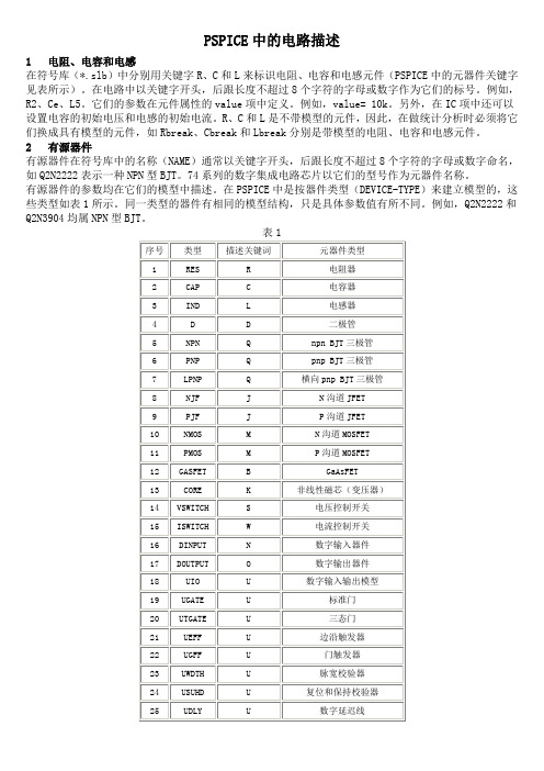
PSPICE中的电路描述1 电阻、电容和电感在符号库(*.slb)中分别用关键字R、C和L来标识电阻、电容和电感元件(PSPICE中的元器件关键字见表所示)。
在电路中以关键字开头,后跟长度不超过8个字符的字母或数字作为它们的标号。
例如,R2、Ce、L5。
它们的参数在元件属性的value项中定义。
例如,value= 10k。
另外,在IC项中还可以设置电容的初始电压和电感的初始电流。
R、C和L是不带模型的元件,因此,在做统计分析时必须将它们换成具有模型的元件,如Rbreak、Cbreak和Lbreak分别是带模型的电阻、电容和电感元件。
2 有源器件有源器件在符号库中的名称(NAME)通常以关键字开头,后跟长度不超过8个字符的字母或数字命名,如Q2N2222表示一种NPN型BJT。
74系列的数字集成电路芯片以它们的型号作为元器件名称。
有源器件的参数均在它们的模型中描述。
在PSPICE中是按器件类型(DEVICE-TYPE)来建立模型的,这些类型如表1所示。
同一类型的器件有相同的模型结构,只是具体参数值有所不同。
例如,Q2N2222和Q2N3904均属NPN型BJT。
在模型库中,有源器件的模型名称(MODELNAME)与符号库中器件名称的命名方法类似。
符号库(扩展名为slb的磁盘文件)与模型库(扩展名为lib的磁盘文件)是通过模型名称建立联系的。
例如,Q2N2222、Q2N2222-X。
电路仿真的精度主要由元器件所选用的模型和模型参数来决定。
PSPICE中选用了较精确的模型,其模型参数也很多,在多数情况下,可以忽略其中许多参数。
PSPICE在分析时使用这些参数的缺省值(default value 计算机自动给出的值,也称为默认值)。
表2中给出了几种器件常用的模型参数。
表2 几种元器件常用的模型参数3 信号源及电源在电路描述中,信号源和电源是必不可少的。
实际上电源可以看作是一种特殊的信号源。
在PSPICE中,信号源被分为两类:独立源和受控源。
用于瞬态分析的五种激励信号

用于瞬态分析的五种激励信号Pspice软件为瞬态分析提供了五种激励信号波形(称为瞬态源)供用户选用。
下面介绍这五种瞬态源的波形特点和描述该信号波形时涉及到的参数。
其中电平参数针对的是独立电压源。
对独立电流源,只需将字母V改为I,其单位由伏特变为安培。
(1).脉冲电源(VPulse):P247习题脉冲信号是在瞬态分析中用得较频繁的一种激励信号。
描述脉冲信号波形涉及到7个参数。
表1列出了这些参数的含义、单位及内定值。
表2给出了不同时刻脉冲信号值与这些参数之间的关系。
下图为一具体实例。
图中给出了该波形对应的参数。
脉冲信号波形(例)表1描述脉冲信号波形的参数注:表中TSTOP是瞬态分析中参数Final Time的设置值;TSTEP是参数Print Step的设置值。
表2脉冲信号电平值与参数的关系(2).分段线性电源(VPWL: Piece-Wise Linear):5.2节分段线性信号波形由几条线段组成。
因此,为了描述这种信号,只需给出线段转折点的坐标数据即可。
下图是一个分段线性信号波形实例。
图中同时给出了描述该波形的数据。
分段线性信号波形(例)(3).调幅正弦电源(VSIN: Sinusoidal Waveform):5.1节描述调幅正弦信号涉及6个参数。
表3列出了这些参数的含义、单位和内定值。
表4给出了调幅正弦信号波形的变化与这6个参数的关系。
下图为一具体实例,图中同时给出了该信号波形对应的参数。
调幅正弦信号波形(例)注:表中TSTOP为瞬态分析中参数Final Time的设置值。
表4 调幅信号波形与参数的关系说明:此处描述的调幅正弦信号只用于瞬态分析。
若阻尼因子与偏置值均为0,则调幅信号成为标准的正弦信号,但是在进行3-6节介绍的AC分析时,本信号并不起作用。
(4).调频电源(VSFFM: Single-FrequencyFrequency-Modulated)描述调频信号需要5个参数,表5列出了这些参数的含义、单位和内定值。
PSpice中产生方波的参数设置
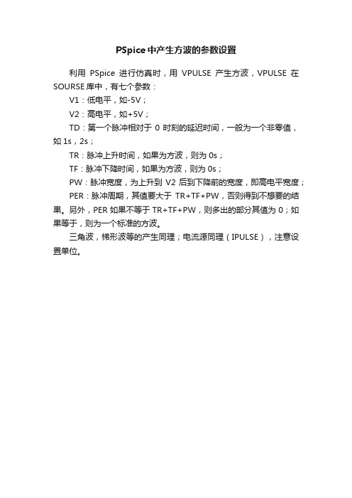
PSpice中产生方波的参数设置
利用PSpice进行仿真时,用VPULSE产生方波,VPULSE在SOURSE库中,有七个参数:
V1:低电平,如-5V;
V2:高电平,如+5V;
TD:第一个脉冲相对于0时刻的延迟时间,一般为一个非零值,如1s,2s;
TR:脉冲上升时间,如果为方波,则为0s;
TF:脉冲下降时间,如果为方波,则为0s;
PW:脉冲宽度,为上升到V2后到下降前的宽度,即高电平宽度;
PER:脉冲周期,其值要大于TR+TF+PW,否则得到不想要的结果。
另外,PER如果不等于TR+TF+PW,则多出的部分其值为0;如果等于,则为一个标准的方波。
三角波,梯形波等的产生同理;电流源同理(IPULSE),注意设置单位。
Pspice仿真类型及不同电源参数

VSFFM属性设置框中各项参数的含义及单位见表1-3。
表1-3 VSFFM的属性参数
参数
含义
单位
VOFF
直流偏移电压
伏特
VAMPL
振幅
伏特
FC
载波频率
赫兹
FM
调制频率
赫兹
MOD
调制因子
无
按图1-15设置参数的VSFFM波形如图1-16所示。
图1-9 VSFFM波形
e)指数信号(VEXP、IEXP)
设置完毕,点击确定按钮。
图1-10 Simulation Settings
3.进行电路仿真
(1)执行菜单命令PSpice/Run,或点击工具按钮,调用PSpice A/D软件对该电路图进行仿真模拟。
(2)依次点击工具按钮、、,则电路图上相应位置依次显示节点电压、支路电流及各元器件上的功率损耗。如图1-29所示。
以上各项填完之后,按确定按钮,即可完成仿真分析类型及分析参数的设置。
另外,如果要修改电路的分析类型或分析参数,可执行菜单命令PSpice/Edit Simulation Profile,或点击工具按钮,在弹出的对话框中作相应修改。
(3)电路的模拟仿真
a)PSpice A/D视窗的启动
执行菜单命令PSpice/Run,或点击工具按钮,即可启动PSpice A/D视窗执行电路的仿真模拟,并且系统可自动调用Probe模块,对模拟结果进行后处理,屏幕显示如图1-5所示。
图1-11 VEXP波形
l瞬态分析的应用
现在通过举例,来说明瞬态分析的应用方法。
例:图1-19所示电路的电压源为分段线性源,其波形如图1-20所示。试对该电路进行瞬态分析。
Pspice使用指南
图 16-7 分析类型对话框
2. 点选你想要模拟的项目,然后进入个别设定视窗。常用的模拟内容有:
AC Sweep:交流扫描分析(包括躁声分析),要找频率响应用这项。 DC Sweep:直流扫描分析,一般的 I-V 特性用这项。 Bias Point Detail:直流工作点分析即可节点的偏压分析,通常一定选,是确省
可以做扫描的不是只有直流电压或交流电压,还有所列的其它参数, 图右必须键入电 源名称或全局参数名,扫描范围及间隔。假如要扫描的参数不只一个,则可使用 Nested Sweep 设定第二个扫描。
3. 进入 DC Sweep 设置窗口后,选 Global Parameter(全局参数)和 Linear(线性扫 描),在 Name 文本框后第一格内写入全局参数名 var,将 Start Value(扫描初长) 设为 1,End Value(扫描终值)设为 1k,Increment(扫描步长)设为 10。单击[OK] 结束操作。如图 16-8。
步骤:1. 绘制电路原理图(所要绘制图如 16-12 所示)
图 16-12 电路原理图
PSpice

1.2 PSpice中的电路描述
Probe :输出波形的后处理程序(也称探针显示器)。可以处理、 显示、打印电路各节点和支路的多种波形(频域、时域、FFT频谱 等)。
Stimulus Editor :信号源编辑器。用于编辑和修改各种信号源。
Parts :模型参数提取程序。Parts程序可以根据产品手册所给出 的电特性参数提取用于PSPICE分析的器件模型参数。器件模型包括: 二极管、BJT、JFET、MOSFET、砷化镓场效应晶体管、运算放大器 和电压比较器等。 Pspice Optimizer :电路设计优化程序。
信号源的参数可在其属性中定义。例如,脉冲源的初始电压V1、脉 冲电压V2、延迟时间TD、上升时间TR、下降时间TF、脉冲宽度PW、 周期PER等,均可在其属性窗中赋值。(看下页)
上面的描述请大家与书后附录一对照,熟悉某个电路符号位于哪个 符号库中,以提高绘制电路图的速度。
1.2 PSpice中的电路描述
一个完整的电路,不仅包括电路的结构,而且还包含各元器件、 信号源及电源的有关参数。电路的结构可以通过元器件符号以及它 们之间的连线来描述;而参数则是在元件属性(Attributes)中描 述的。
描述一个元器件通常包括元器件符号名称、元器件在电路中的 标号、元器件参数值等几部分内容。由于有源器件的参数较多,它 们不直接在属性中给出,而是用专门的模型(Model)来描述,属 性中只给出它的模型名称。仿真时,PSPICE从模型库中调出该元 器件的参数值进行仿真。下面对电路元件的描述作进一步的介绍。
12pspice几种主要的独立源类型名电源及信号源类型应用场合dc固定直流源直流电源直流特性分析ac固定交流源正弦稳态频率响应sin正弦信号源瞬态分析正弦稳态频率响应pulse脉冲源瞬态分析pwl分段线性源瞬态分析src简单源可当作acdc或瞬态源12pspice受控源元器件描述关键词受控源类型电流控制电压源12pspice122电路符号的属性属性值和属性表具体到实例中讲述见后
Pspice简明教程

Pspice 教程Pspice 教程课程内容:补充说明(1 网表输出)(2 如何下载和使用新元件模型)1.直流分析2.交流分析3.参数分析4.瞬态分析5.蒙特卡洛分析6.温度分析7.噪声分析8.傅利叶分析9.静态直流工作点分析附录A: 关于Simulation Setting 的简介附录B:关于测量函数的简介附录C:关于信号源的简介使用软件的说明:CADENCE仿真可以在Capture或者HDL界面下,1Capture 的优点是界面简洁,容易学习,使用广泛。
HDL 的界面比较复杂,而且各种规则约束较多,2 他们在使用的原理图库不同,Capture的原理图以*.olb的形式存放在TOOL-capture -library中,而HDL的原理图、封装形式、以及物理信息都集成在share-library下的各自元件中;3两者的仿真模型库相同,都在TOOL-pspice中。
所以从仿真效果来看,两者没有区别。
4 HDL的好处是当完成原理图仿真后,可以直接输出网表,到APD版图中,供自动布局用。
一.直流分析直流分析:PSpice 可对大信号非线性电子电路进行直流分析。
它是针对电路中各直流偏压值因某一参数(电源、元件参数等等)改变所作的分析,直流分析也是交流分析时确定小信号线性模型参数和瞬态分析确定初始值所需的分析。
模拟计算后,可以利用Probe 功能绘出Vo-Vi 曲线,或任意输出变量相对任一元件参数的传输特性曲线。
首先我们开启DesignCapture / Capture CIS. 打开如下图所示的界面( Fig.1) 。
( Fig 1) 我们来建立一个新的工程 ( Fig.2)( Fig.2)我们来选取一个新建的工程文件! 我们可以看到以下的提示窗口。
(Fig.3)(Fig.3) 我们可以给这个工程取个名字,因为我们要做Pspice 仿真,所以我们要勾选第一个选项,在标签栏中选中!其它的选项是什么意思呢?Analog or Mixed A/D 数模混合仿真PC Board Wizard 系统级原理图设计Programmable Logic Wizard CPLD 或FPGA 设计Schematic 原理图设计接下来我们看到了Pspice 工程窗口,即我们的原理图窗口属性的选择。
Pspice器件模型参数说明

Pspice 器件模型参数说明1、二极管模型及主要参数二极管模型参数如表1所示 名称 符号 SPIC 名称 单位 缺省值 反向饱和电流(Saturation current) I S IS A 10-14 欧姆电阻(Ohmic resistance) R S RS Ω 0 发射系数(Emission coefficient) n N 1 渡越时间(Transit time) τT TT s 0 零偏置电容(Zero-bias junction capacitance) C j0 CJ0 F 0 结电压(Junction potential) V 0 VJ V 1 电容梯度因子(Grading coefficient) m M 0.5 反向击穿电压(Reverse breakdown voltage) V ZK BV V ∞ 反向击穿电流(Current at breakdown voltage) I ZK IBV A 10-10仿真时采用理想二极管,参数不需要设置。
参数说明:I S :PN 结反向扩散电流,该值远小于PN 结反向(漏)电流,因为它为包括反向空间电荷区产生的电流、表面复合电流、表面沟道电流和表面漏导电流。
n :一般n =1,测量:正向特性线性区 )/ln(2121D D D D I I V V kT q n −=C j0: CD =C d +C j =m nU U V U C eI U )1()1(0D 0j s TTTD −+−τ0j T T 2)1(TDC e I U nU Us+−≈τV 0:0.7-0.8Vm : 0.3-0.5, 一般为0.332、 稳压管模型及主要参数模型参数如表1所示,参数设置如下: V ZK =U Z I ZK =I Zmin3、 晶体管模型及主要参数模型参数如表2所示名称符号 SPIC 名称 单位 缺省值 传输饱和电流 I S IS A 10-16 正向电流增益 βF BF100 反向电流增益 βR BR 1集电极电阻 R CC’ RC Ω 0 发射极电阻 R EE’ RE Ω 0 基极电阻R BB’ RB Ω 0 理想正向渡越时间τF TFs 0理想反向渡越时间 τR TR s 0 发射结零偏置势垒电容 C je0 CJE F 0 发射结电容梯度因子 m BEJ MJE 0.33 发射结内建电势 V 0e VJE V 0.75 集电结零偏置势垒电容 C jc0 CJC F 0 集电结零偏置势垒电容 m BCJ MJC 0.33 集电结零偏置势垒电容 V 0c VJC V 0.75一般参数设置如下:RB: r bb’RE, RC: 一般设为0 V 0e : =U BE , 一般为0.7V V 0c : 一般为0.75V其它参数说明:0je me0BE 0je je C 2)V U 1(C C ≈−=,此处m BE 约为0.5mc 0CB 0)V U 1(C C +=μμ,此处m BC 约为0.2-0.5 参数设置经验:C je0=0.5C π,C jc0=C μ=C ob4、 MOSFET 模型及主要参数i D 与u GS 、u DS 之间的关系:2GS(th)DO n 2GS(th)GS n 2GS(th)GS n D 2DS DS GS(th)GS n D oxn n n 2GS(th)GS ox n D ox ox oxoxox U I k )U U (k )U U )(L W('k 21i U 21U )U U )[(L W ('k i C 'k )L W()U U )(L W )(C (21i )T (T C =−=−=−−==−==恒流区:可变电阻区:沟道宽长比载流子迁移率,二氧化硅厚度二氧化硅介电常数,μμμεε模型参数设置:KP=k n ’, VT0=阈值电压U GS(th)。
三极管的Pspice模型参数

附件A、三极管的Pspice模型参数.Model <model name> NPN(PNP、LPNP) [model parameters]第 1 页共9页第 2 页共9页附件B、PSpice Goal Function第 3 页共9页附件CModeling voltage-controlled and temperature-dependent resistorsAnalog Behavioral Modeling (ABM) can be used to model a nonlinear resistor through use of Ohm抯 law and tables and expressions which describe resistance. Here are some examples.Voltage-controlled resistorIf a Resistance vs. Voltage curve is available, a look-up table can be used in the ABM expression. This table contains (Voltage, Resistance) pairs picked from points on the curve. The voltage input is nonlinearly mapped from the voltage values in the table to the resistance values. Linear interpolation is used between table values.Let抯 say that points picked from a Resistance vs. Voltage curve are:Voltage ResistanceThe ABM expression for this is shown in Figure 1.第 4 页共9页Figure 1 - Voltage controlled resistor using look-up tableTemperature-dependent resistorA temperature-dependent resistor (or thermistor) can be modeled with a look-up table, or an expression can be used to describe how the resistance varies with temperature. The denominator in the expression in Figure 2 is used to describe common thermistors. The TEMP variable in the expression is the simulation temperature, in Celsius. This is then converted to Kelvin by adding 273.15. This step is necessary to avoid a divide by zero problem in the denominator, when T=0 C.NOTE: TEMP can only be used in ABM expressions (E, G devices).Figure 3 shows the results of a DC sweep of temperature from -40 to 60 C. The y-axis shows the resistance or V(I1:-)/1A.第 5 页共9页Figure 2 - Temperature controlled resistorFigure 3 - PSpice plot of Resistance vs. Temperature (current=1A)Variable Q RLC networkIn most circuits the value of a resistor is fixed during a simulation. While the value can be made to change for a set of simulations by using a Parametric Sweep to move through a fixed sequence of values, a voltage-controlled resistor can be made to change dynamically during a simulation. This is illustrated by the circuit shown in Figure 5, which employs a voltage-controlled resistor.第 6 页共9页Figure 4 - Parameter sweep of control voltageThis circuit employs an external reference component that is sensed. The output impedance equals the value of the control voltage times the reference. Here, we will use Rref, a 50 ohm resistor as our reference. As a result, the output impedance is seen by the circuit as a floating resistor equal to the value of V(Control) times the resistance value of Rref. In our circuit, the control voltage value is stepped from 0.5 volt to 2 volts in 0.5 volt steps, therefore, the resistance between nodes 3 and 0 varies from 25 ohms to 100 ohms in 25 ohm-steps.第7 页共9页Figure 5 - Variable Q RLC circuitA transient analysis of this circuit using a 0.5 ms wide pulse will show how the ringing differs as the Q is varied.Using Probe, we can observe how the ringing varies as the resistance changes. Figure 6 shows the input pulse and the voltage across the capacitor C1. Comparing the four output waveforms, we can see the most pronounced ringing occurs when the resistor has the lowest value and the Q is greatest. Any signal source can be used to drive the voltage-controlled resistance. If we had used a sinusoidal control source instead of a staircase, the resistance would have varied dynamically during the simulation.第8 页共9页Figure 6 - Output waveforms of variable Q RLC circuit第9 页共9页。
Pspice元件库介绍
1.1_SHOT : 10个杂项器件,其中有54,74,CD的2.7400~74S : 74系列的器件3.AA_IGBT : IGBT是强电流、高压应用和快速终端设备用垂直功率MOSFET4.AA_MISC : 杂项DIODE MOSFET5.ABM : 各种数学运算单元,如cos,sin,log,hipass,lowpass等,还有E/F/H/G等元件.6.ADV_LIN : ALD系列的线性放大器7.ANA_SWIT : 模拟开关8.ANALOG和ANALOG_P : 通用模拟器件,R,C,L9.ANL_MISC : 杂项模拟器件,如三相变压器,555,RELAY,SWITCH,VCO10.ANLG_DEV : AD公司放大器,电压参考器件,11.APEX : APEX公司PA/AM 系列运放12.APEX_PWM : APEX公司系列PWM控制器13.ASW : DG系列模拟开关14.BIPOLAR~BJPD : 三极管15.BREAKOUT: 用于最坏情况分析的元件。
RAM,ROM,DA8/10/12,AD/8/10/12,R,SWITCH,Q,POT(滑动变阻器),M,X(TRANSFORER)16.BUF & BUFF_BRN : BUFFERS17.CD4000 : CD系列器件18.CEL : NE系三极管LINR : CLC系列BUFF,OPA20.CONTROLLER : 电源控制电路,DC TO DC21.CORES : 磁芯22.DARLNGTN : EPITAXIAL SILICON TRANSISTOR23.DATACONV : AD,DA24.DI : DIODE25.DIF : DIODE BRIDGE26.DIG_ECL : D Flip-Flop28.DIG_GAL : Generic Array Logic29.DIG_MISC : mixed digital device30.DIG_PAL : programable Array Logic31.DIG_PRIM : Generic digitial device: and,add,Flip_Flop32.DIH : diode pull-up and pull-down network33.DIODE : diode34.DIV : diode v35.DIZ : diode z36.DRI : MIXED37.EBIPLOAR : bipolar38.EDIODE : diode39.ELANTEC : ELANTEC半导体公司器件,运放,门电路等40.EPCOS : EPCOS公司器件,磁珠,压每电阻,NTC等。
三极管的Pspice模型参数详细说明

正向和反向放大倍数的温度影响系数
XTF
transit time bias dependence coefficient
0.0
传递时间系数
XTI (PT)
IS temperature effect exponent
3.0
IS的温度影响系数
附件B、PSpice Goal Function
特征函数
功能说明
0.0
发射结电容
CJS (CCS)
Substrate zero-bias p-n capacitance
farad
0.0
零偏极电极-衬底电容
EG
bandgap voltage (barrier height)
eV
1.11
FC
forward-bias depletion capacitor coefficient
HPBW (1, db_level)
查找第一次比最大值低db_level db的x坐标。(上升沿)
LPBW (1, db_level)
与HPBW类似,只是用于下降沿。
Maxr (1, begin-x, end-x)
查找区间的最大值。
Overshoot (1)
计算最大值与终点之间y轴坐标差与终点值的百分比。
0C
T_REL_LOCAL
relative to AKO model temperature
0C
VAF (VA)
forward Early voltage
volt
infinite
VAR (VB)
reverse Early voltage
volt
infinite
VJC (PC)
pspice二级管参数总结
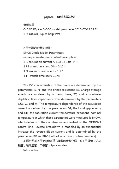
pspice二级管参数总结查看文章OrCAD PSpice DIODE model parameter 2010-07-15 22:311.从OrCAD PSpice help文档:2.国外网站的相关介绍:SPICE Diode Model Parametersname parameter units default example ar1 IS saturation current A 1.0e-14 1.0e-14 *2 RS ohmic resistanc Ohm 0 10 *3 N emission coefficient - 1 1.04 TT transit-time sec 0 0.1nsThe DC characteristics of the diode are determined by the parameters IS, N, and the ohmic resistance RS. Charge storage effects are modeled by a transit time, TT, and a nonlinear depletion layer capacitance whic determined by the parameters CJO, VJ, and M. The temperature dependence of the saturation current is defined by the parameters EG, the band gap energy and XTI, the saturation current temperature exponent. nominal temperature at which these parameters were measured is TNOM, which defaults to the circuit-wi value specified on the .OPTIONS control line. Reverse breakdown is modeled by an exponential increase the reverse diode current and is determined by the parameters BV and IBV (both of which are positive numbers).3. 国外网站关于PSpice 其它模型的参数介绍:如(三极管,达林顿管,场效应管,二极管)Spice modelsIntroductionThe MOD model fileThe ZMODELS.LIB library fileModel parameters and limitationso Bipolarso Darlingtonso MOSFETso DiodesFurther informationIntroductionZetex have created Spice models for a range of semiconductor components. Models included are Schottky varicap, high-performance bipolar (high current, low VCE(sat)), higher voltage bipolar, bipolar Darlingto and MOSFET transistors. This range is continuously under review as new products are introduced and retrospective models are generated for existing products.The Spice models are available in two formats:1. A separate Spice model text file for each Zetex device type for which a model is presently availabThese can be accessed from the Product Quickfinder2.All the available Zetex device models are collected together into a single .LIB text file calledZMODELS.LIB.A generic symbol library file is available called ZETEXM.SLB that enables Windows? versions of PSpic use the Zetex spice models. Further information on the symbol library, including installation instructions be found in the text file called ZETEXM.TXTThe MOD Model FileEach of these files is a Spice model for a single device. Theycan be loaded into your simulation simply b employing the Spice command <.include device_name.mod>. Only the device types specifically required the circuit under simulation need be included in this way. All diode and bipolar transistor models are simp <.model> files. However, Darlington transistors and MOSFET models are multi-component subcircuits an such are supplied as <.subckt> files.The diode models should be included in circuit files using the normal Spice reference .Bipolar transistor models should be included using .All other models should be referenced as subcircuits i.e. in the form for Darlington transistors, and for MOSFETs.The ZMODELS.LIB Library FileUsers may prefer to use the model library. This library is a collection of all Zetex Spice models exactly as t appear in the individual model files. By using the statement <.lib zmodels.lib>, Spice will be able to acce any model within the library without the need for multiple <.include> statements.Note:All subcircuits, whether in the library or as individual model files use the same connection sequence as Sp for single element models, thus easing their use.Model parameters and limitationsBipolarsDarlingtonsMOSFETsDiodesBipolarsAll bipolar transistor and Darlington models are based on Spice's modified Gummel-Poon model. A typic model for a singletransistor is shown as follows:*Zetex FMMT493A Spice Model v1.0 Last Revised 30/3/06*.MODEL FMMT493A NPN IS =6E-14 NF =0.99 BF =1100 IKF=1.1+NK=0.7 VAF=270 ISE=0.3E-14 NE =1.26 NR =0.98 BR =70 IKR=0.5+VAR=27 ISC=1.2e-13 NC =1.2 RB =0.2 RE =0.08 RC =0.08 RCO=8+GAMMA=5E-9 CJC=15.9E-12 MJC=0.4 VJC=0.51 CJE=108E-12+MJE=0.35 VJE=0.7 TF =0.8E-9 TR =55e-9 XTB=1.4 QUASIMOD=1*In the bipolar model:IS and NF control Icbo and the value of Ic at medium bias levels.ISE and NE control the fall in hFE that occurs at low Ic.BF controls peak forward hFE and XTB controls how it varies with temperature.BR controls peak reverse hFE i.e. collector and emitter reversed.IKF and NK control the current and the rate at which hFE falls at high collector currents.IKR controls where reverse hFE falls at high emitter currents.ISC and NC controls the fall of reverse hFE at low currents.RC, RB and RE add series resistance to these device terminals.VAF controls the variation of collector current with voltage when the transistor is operated in its lin region.VAR is the reverse version of VAF.CJC, VJC and MJC control Ccb and how it varies with Vcb.CJE, VJE and MJE control Cbe Ccb and how it varies with Veb.TF controls Ft and switching speeds.TR controls switching storage times.RCO, GAMMA, QUASIMOD control the quasi-saturation region.Some standard bipolar transistor Spice models may not include a parameter that allows BF, the hFE parame to vary with temperature. If XTB is absent it defaults to zero, e.g. no temperature dependence. If hFE temperature effects are of interest and XTB is not modeled then the following values may be used to provid estimate or a starting point for further investigation:It is suggested that the appropriate datasheet hFE profile is examined, and a Spice test circuit created that simulates the device in question and generates a set of hFE curves. Two or three such iterations should normally be sufficient to define a value for XTB in each case. Please remember that these notes are only a rough guide as to the effect of model parameters. Also, many of the parameters are interdependent so adjus one parameter can affect many device characteristics.At Zetex, we have endeavored to make the models perform as closely to actual samples as possible but so compromises are forced which can result in simulation errors under some circumstances. The main areas error observed so far have been: Spice is often over optimistic in the hFE a transistor will give when operated above its data sheet current ratings. This is particularly true for a high voltage transistor operated at a low collector-em voltage and quasi-saturation parameters RCO,GAMMA and QUASIMOD have been introduced t improve the models in this region.Spice can be pessimistic when predicting switching storage time when current is extracted from th base of a transistor to speed turn-off.DarlingtonsThese are subcircuits using a standard transistor model. A Darlington model is shown as follows:**Zetex FZT605 Spice Model v1.0 Last revision 27/04/05*.SUBCKT FZT605 1 2 3* C B EQ1 1 2 4 SUB605Q2 1 4 3 SUB605 3.46*.MODEL SUB605 NPN IS=4.8E-14 BF=170 etc..ENDS FZT605**$Note:Because Zetex Darlingtons are monolithic, the two transistors used are identical in all respects other than s (The number at the end of the Q2 line multiplies the size of the SUB605 transistor by 3.46 - the ratio of th areas of the input and output transistors for this device).MOSFETsNone of Spice's standard MOSFET models fit the characteristics of trench or vertical MOSFETs too well. Consequently the models of MOSFET's supplied have been madeusing subcircuits that include additiona components to improve simulation accuracy. A typical less complex MOSFET model is shown as follows **ZETEX ZXMN3A14F Spice Model v1.0 Last revision 31/5/06 *.SUBCKT ZXMN3A14F 30 40 50*------connections-------D-G-SM1 6 2 5 5 Nmod L=1.16E-6 W=0.76M2 5 2 5 6 Pmod L=1.3E-6 W=0.35RG 4 2 4.5RIN 2 5 1E12RD 3 6 Rmod 0.04RS 5 55 Rmod 0.015RL 3 5 3E9C1 2 5 8.5E-12C2 3 4 3E-12D1 5 3 DbodymodLD 3 30 0.5E-9LG 4 40 1.0E-9LS 55 50 1.0E-9.MODEL Nmod NMOS (LEVEL=3 TOX=5.5E-8 NSUB=5E16 VTO=2.13+KP=2.5E-5 NFS=2E11 KAPPA=0.06 UO=650 IS=1E-15 N=10).MODEL Pmod PMOS (LEVEL=3 TOX=5.5E-8 NSUB=1.5E16 +TPG=-1 IS=1E-15 N=10).MODEL Dbodymod D (IS=6E-13 RS=.025 IKF=0.1 TRS1=1.5e-3+CJO=150e-12 BV=33 TT=12e-9).MODEL Rmod RES (TC1=2.8e-3 TC2=0.8E-5).ENDS ZXMN3A14F**$*In the MOSFET model:L relates to a process parameter.W relates to a process parameter.TOX relates to a process parameter.NSUB relates to a process parameter.VTO defines Vgs(th).KP controls Gm.NFS fast surface state density.KAPPA saturation field factor.UO mobility.RS and RD add series terminal resistance with temperature characteristic modeled.IS and N suppress the behavior of the MOSFET model's default body diode.CGDO, derived from process related parameters, controls Crss.CGSO, derived from process related parameters, controls Ciss.CBD, derived from process related parameters, controls Coss.In this trench MOSFET the NMOS models the walls of the trench and the PMOS models the bottom of th trench. Added to the Spice standard MOSFET models are a gate resistor to control switching speeds, gate source and drain-source resistors to control leakage, drain and source series resistance, a drain-source diod accurately reflect the performance of the MOSFET's body diode and inductors to model inductance inside package.Recent MOSFET models mirror the performance of the realdevices reasonably well in most areas. One a not covered well by the older less complex models is the way that Crss and Coss vary with drain-source voltage. Thus if the less complex models are used at a drain-source voltage well away from datasheet capacitance definition voltages and capacitance is critical, then the values used for CGSO and CGDO may need adjustment.DiodesThe Tuner diode and Schottky Diode ranges use a standard Spice diode model and a typical file appears a follows: **Zetex ZC830A Spice Model v1.0 Last Revised 4/3/92*.MODEL ZC830A D IS=5.355E-15 N=1.08 RS=0.1161 XTI=3 + EG=1.11 CJO=19.15E-12 M=0.9001 VJ=2.164 FC=0.5+ BV=45.1 IBV=51.74E-3 TT=129.8E-9+ ISR=1.043E-12 NR=2.01**NOTES: FOR RF OPERATION ADD PACKAGE INDUCTANCE 0F 2.5E-9H AND SET*RS=0.68 FOR 2V, 0.60 FOR 5V, 0.52 FOR 10V OR 0.46 FOR 20V BIAS.**$*In the diode model:IS controls forward and reverse current against voltage.N controls forward current against voltage.RS controls forward voltage at high current.CJO, M and VJ control variation of capacitance with voltage.BV and IBV control reverse breakdown characteristics.TT controls switching reverse recovery characteristics.ISR and NR control reverse biased leakage.EG controls barrier height.FC forward bias depletion capacitance coefficient.For operation at RF (which would be the norm for a varicap or tuner diode) it is recommended that a 2.5n series inductor be added as an extra circuit element to correct for the inherent package inductance, this va will change with package size.Also for some models data is available to enable the RS parameter better model Q at voltages other than t specified condition.索取相关资料& 与我讨论博主联系方式:。
- 1、下载文档前请自行甄别文档内容的完整性,平台不提供额外的编辑、内容补充、找答案等附加服务。
- 2、"仅部分预览"的文档,不可在线预览部分如存在完整性等问题,可反馈申请退款(可完整预览的文档不适用该条件!)。
- 3、如文档侵犯您的权益,请联系客服反馈,我们会尽快为您处理(人工客服工作时间:9:00-18:30)。
Pspice仿真——常用信号源及一些波形产生方法首先说说可以应用与时域扫描的信号源。
在Orcad Capture的原理图中可以放下这些模型,然后双击模型,就可以打开模型进行参数设置。
参数被设置了以后,不一定会在原理图上显示出来的。
如果想显示出来,可以在某项参数上,点击鼠标右键,然后选择di splay,就可以选择让此项以哪种方式显示出来了。
1.Vsin 这个一个正弦波信号源。
相关参数有:
VOFF:直流偏置电压。
这个正弦波信号,是可以带直流分量的。
VAMPL:交流幅值。
是正弦电压的峰值。
FREQ:正弦波的频率。
PHASE:正弦波的起始相位。
TD:延迟时间。
从时间0开始,过了TD的时间后,才有正弦波发生。
DF:阻尼系数。
数值越大,正弦波幅值随时间衰减的越厉害。
2.Vexp 指数波信号源。
相关参数有:
V1:起始电压。
V2:峰值电压。
TC1:电压从V1向V2变化的时间常数。
TD1:从时间0点开始到TC1阶段的时间段。
TC2:电压从V2向V1变化的时间常数。
TD2:从时间0点开始到TC2阶段的时间段。
3.Vpwl 这是折线波信号源。
这个信号源的参数很多,T1~T8,V1~V8其实就是各个时间点的电压值。
一种可以设置8个点的坐标,用直线把这些坐标连起来,就是这个波形的输出了。
4.Vpwl_enh 周期性折线波信号源。
它的参数是这样的:
FIRST_NPAIRS:第一转折点坐标,格式为(时间,电压)。
SECOND_NPAIRS:第二转折点坐标。
THIRD_NPAIRS:第三转折点坐标。
REPEAT_VALUE:重复次数。
5.Vsffm 单频调频波信号源
参数如下:
VOFF:直流偏置电压。
VAMPL:交流幅值。
正弦电压峰值。
FC:载波信号频率
MOD:调制系数
FM:被调制信号频率。
函数关系:Vo=VOFF+VAMPL×sin×(2πFC×t+MOD×sin(2πFM×t))
6.Vpulse 脉波信号源。
这大概是我最常用到的信号源了。
用它可以实现很多种周期性的信号:方波、矩形波、三角波、锯齿波等。
可以用来模拟和实现上电软启动、可以用来产生PWM驱动信号或功率信号等等。
参数如下:
V1:起始电压
TD:从时间零开始到V1开始跳变到V2的延迟时间。
TR:从V1跳变到V2过程所需时间。
TF:从V2跳回到V1过程所需时间。
PW:脉冲宽度,就是电压为V2的阶段的时间长度。
PER:信号周期
在以上的几种信号源中,还有两个参数,AC与DC。
说实话,我不是很清楚是做什么用的。
一般这两个参数都是空着不要设置的。
与以上电压源信号对应的还有一组电流源信号,只需要把模型名称的第一个字母由V 改成I就可以得到。
其相关参数的意义是相同的。
唯一的区别就是把电压信号变成电流信号。
大家可以自己去看看学习一下。
还有几个比较重要的信号源:
1.VDC
不用多说了,这个是最基本的电压源,可以作为直流信号源,或者电源给电路供电。
唯一需要设置的参数就是电压值。
2.VAC
这个信号源有两个参数
DC:直流偏置值。
ACMAG:交流电压幅值。
ACPHASE:交流起始相位,一般不设置这项。
这个交流信号源,是用来做频率扫描用的,可以用来观察一个电路的频域特性。
同样的,也有与上面两个信号源相对应的电流信号源。
下面,我们来通过仿真,实际尝试一下这些模型的应用,先在Capture环境中建立新项目,在原理图中放置如下的模型,并设置相关参数:
然后设置10ms时间的时域扫描,步长100ns,待仿真完成后,入图所示自最后一个开始,每放一个探头,就在仿真结果的窗口中选择一次菜单plot->add plot to windo w。
然后在调整仿真结果的坐标轴,把XY轴的坐标表格细节换成点状,便于观察波形。
可以看到如下波形:
其中,最下面的三个波形是用Vpulse这个模型通过设置不同的参数构造的矩形波、三角波和锯齿波。
接下来,让我们看看VAC这个模型,是如何应用与频域扫描的。
首先建立一个如下图的原理图,并在输入端放一个Vin的网络标识,在RC的输出放一个VRC的网络标识,在LC的输出放一个VLC的网络标识。
然后,设定如下图的AC扫描:
扫描围不能从0开始,这里是从1Hz开始,扫描到30KHz,在这个围扫描10000
个点。
频率坐标采用以10的对数坐标。
扫描结束后,先选择plot->add plot to windo w,把扫描结果的屏幕分成上下两个,上面的用来显示幅频特性,下面的用来显示相频特
性。
先点击显示波形图的半部分,然后点击。
这个工具栏按钮,添加一个波形,在弹出的对话框里,从右边选择函数DB(),然后在出来的DB()函数括号先点击左边信号列表里的V(VRC),再输入一个除号“/”,再点击V(Vin)。
得到一个函数表达式DB(V(VRC) /V(Vin))。
见下图
然后点击OK,就可以得到RC那部分电路的幅频特性。
同样的操作,继续在波形图
上半部分添加LC部分的幅频特性。
在波形图下半添加两个电路的相频特性。
相频特性是
用的函数P()。
最后,我们可以得到如下的结果:
由图中可以看出,LC电路的最大相移为180度,而RC为90度。
而过了极点之后,LC电路的幅值下降斜率是RC的2倍。
这是与理论上的结果是一致的。
这里就不细述了。
对于一些复杂的信号,我们可以通过一些模型之间进行运算而得到。
例如,中波调幅的无线电信号,就是用一个频率作为载波,用另一个频率去调制它,从而实现了在高频载波中包含音频信息的一种信号。
这个怎么实现呢?我们可以通过乘法器来实现,看下图:
图中,V1信号为低频音频信号,V2为高频载波信号。
用一个乘法器实现了用V1去调制V2,设置一个2ms的时域扫描看看结果吧:
最近论坛里LLC电路比较流行。
我们知道,LLC是变频控制的。
需要用反馈电路来控制电路的驱动频率。
那么如何实现可以调节频率的信号源呢?我们上面介绍的几个信号源,频率一旦设定好,就不能更改了,怎么办呢?
我们可以用VCO系列的压控信号源。
例如下图:
我在这里用了一个折线波信号源和一个压控方波振荡器。
折现波信号源用来产生一个从5V到0V的负斜率的电压,模拟电源的启动的软启动过程。
压控振荡器为了便于观察,我把中心频率设定在1K。
另外,我发现,这个压控振荡器的最低频率是在(VMAX+VMIN)/ 2的地方,那么为了实现0~5V围频率的变化,我把VMAX设定在5V,VMIN设定在-5V,这样当输入在5~0V之间变化的时候,输出的信号的频率在50KHz在1KHz之间变化。
进行一个长度为10ms的时域仿真,让我们看看仿真的结果吧:
可以看到当最后输入电压为0V的时候,VCO的输出信号频率也稳定在了1KHz上。
如此我们就得到了通过电压调节频率的一个电路。
仿真LLC闭环就方便多了。
接下来,让我们想想,如何实现PWM的脉宽,从低占空比到高占空比逐渐变化,从而实现PWM电源的软启动呢?可以用一个锯齿波信号、一个折线波信号,一个理想运放作为比较器来实现。
看原理图:
为了便于观察,信号源的频率取的比较低。
下面是仿真结果,把结果输出在上下两个部分,便于观察:
从仿真结果可以看到,PWM的脉宽从小的占空比逐渐增加到大占空比。
从而可以用这个方法来实现电源的软启动过程。
有了软启动的这个过程,就可以让我们电路的仿真与实际工作的表现更加接近了。