FPGA可编程逻辑器件芯片XQ4VK60-10FF1148M中文规格书
FPGA可编程逻辑器件芯片XQ4VFX60-10EF672M中文规格书
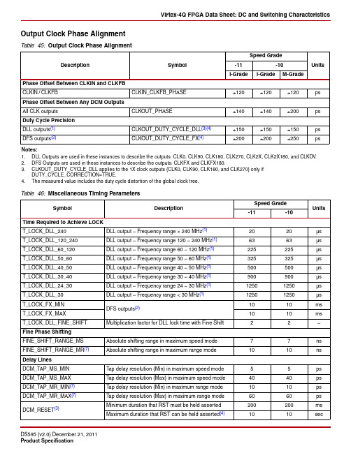
Output Clock Phase Alignment Table 45:Output Clock Phase AlignmentDescription SymbolSpeed GradeUnits -11-10I-Grade I-Grade M-GradePhase Offset Between CLKIN and CLKFBCLKIN/CLKFB CLKIN_CLKFB_PHASE±120±120±120ps Phase Offset Between Any DCM OutputsAll CLK outputs CLKOUT_PHASE±140±140±200ps Duty Cycle PrecisionDLL outputs(1)CLKOUT_DUTY_CYCLE_DLL(3)(4)±150±150±150ps DFS outputs(2)CLKOUT_DUTY_CYCLE_FX(4)±200±200±250psNotes:1.DLL Outputs are used in these instances to describe the outputs: CLK0, CLK90, CLK180, CLK270, CLK2X, CLK2X180, and CLKDV.2.DFS Outputs are used in these instances to describe the outputs: CLKFX and CLKFX180.3.CLKOUT_DUTY_CYCLE_DLL applies to the 1X clock outputs (CLK0, CLK90, CLK180, and CLK270) only ifDUTY_CYCLE_CORRECTION=TRUE.4.The measured value includes the duty cycle distortion of the global clock tree.Table 46:Miscellaneous Timing ParametersSymbol DescriptionSpeed GradeUnits -11-10Time Required to Achieve LOCKT_LOCK_DLL_240DLL output – Frequency range > 240MHz(1)2020µs T_LOCK_DLL_120_240DLL output – Frequency range 120 – 240MHz(1)6363µs T_LOCK_DLL_60_120DLL output – Frequency range 60 – 120MHz(1)225225µs T_LOCK_DLL_50_60DLL output – Frequency range 50 – 60MHz(1)325325µs T_LOCK_DLL_40_50DLL output – Frequency range 40 – 50MHz(1)500500µs T_LOCK_DLL_30_40DLL output – Frequency range 30 – 40MHz(1)900900µs T_LOCK_DLL_24_30DLL output – Frequency range 24 – 30MHz(1)12501250µs T_LOCK_DLL_30DLL output – Frequency range < 30MHz(1)12501250µsT_LOCK_FX_MINDFS outputs(2)1010msT_LOCK_FX_MAX1010ms T_LOCK_DLL_FINE_SHIFT Multiplication factor for DLL lock time with Fine Shift22–Fine Phase ShiftingFINE_SHIFT_RANGE_MS Absolute shifting range in maximum speed mode77ns FINE_SHIFT_RANGE_MR(7)Absolute shifting range in maximum range mode1010ns Delay LinesDCM_TAP_MS_MIN T ap delay resolution (Min) in maximum speed mode55ps DCM_TAP_MS_MAX T ap delay resolution (Max) in maximum speed mode4040ps DCM_TAP_MR_MIN(7)T ap delay resolution (Min) in maximum range mode1010ps DCM_TAP_MR_MAX(7)T ap delay resolution (Max) in maximum range mode6060psDCM_RESET(3)Minimum duration that RST must be held asserted200200ms Maximum duration that RST can be held asserted(4)1010secDCM_INPUT_CLOCK_STOPMaximum duration that CLKIN and CLKFB can be stopped (5)(6)100100msAttribute Min Max CLKFX_MULTIPL Y 232CLKFX_DIVIDE132SymbolDescriptionSpeed Grade Units -11-10Table 53:Global Clock Setup and Hold for LVCMOS25 Standard, With DCM in Source-Synchronous ModeSymbol Description DeviceSpeed GradeUnits -11-10I-Grade I-Grade M-GradeExample Data Input Setup-and-hold Times Relative to a Forwarded Clock Input Pin, Using DCM and Global Clock Buffer.(1)(3)T PSDCM_0/T PHDCM_0No Delay Global Clock and IFFwith DCM inSource-Synchronous Mode(2)XQ4VLX25–––0.07/1.09ns XQ4VLX40––0.37/1.19–0.03/1.19ns XQ4VLX60––0.32/1.29–0.11/1.29ns XQ4VLX80–0.38/1.34––ns XQ4VLX100–0.31/1.41–0.31/1.57–ns XQ4VLX160––0.31/1.89–ns XQ4VSX55––0.32/1.52–0.09/1.52ns XQ4VFX60––0.43/1.74–0.25/1.77ns XQ4VFX100–0.38/1.75––nsNotes:1.The timing values were measured using the fine-phase adjustment feature of the DCM. These measurements include CLK0 DCM jitter.Package skew is not included in these measurements.2.IFF=input flip-flop.3.For situations where clock and data inputs conform to different standards, adjust the setup-and-hold values accordingly using the valuesshown in IOB Switching Characteristics(1)(2), page13.4.Setup time has +150ps offset for operation outside of the industrial temperature range.Table 54:Global Clock Setup and Hold for LVCMOS25 Standard, Without DCMSymbol Description DeviceSpeed GradeUnits -11-10I-Grade I-Grade M-GradeInput Setup-and-Hold Time Relative to Global Clock Input Signal for LVCMOS25 Standard.(1)T PSFD/T PHFD Full Delay Global Clock andIFF without DCM(2)XQ4VLX25–– 2.72/0.50ns XQ4VLX40– 3.06/0.44 3.11/0.44ns XQ4VLX60– 3.50/0.34 3.53/0.37ns XQ4VLX80 2.96/0.26––ns XQ4VLX100 5.83/–0.09 6.76/–0.01–ns XQ4VLX160– 3.76/0.88–ns XQ4VSX55– 2.97/0.98 3.02/0.98ns XQ4VFX60– 3.54/0.59 3.58/0.62ns XQ4VFX100 2.21/1.31––nsNotes:1.Setup time is measured relative to the global clock input signal with the fastest route and the lightest load. Hold time is measured relative tothe global clock input signal with the slowest route and heaviest load.2.IFF = input flip-flop or latch.3. A zero “0” hold time listing indicates no hold time or a negative hold time. Negative values can not be guaranteed best-case, but if a “0” islisted, there is no positive hold time.Symbol Description DeviceSpeed GradeUnits -11-10T DCD_CLK Global Clock T ree Duty CycleDistortion(1)All150150psT CKSKEW Global Clock T ree Skew(2)XQ4VLX25–110ps XQ4VLX40–180ps XQ4VLX60–180ps XQ4VLX80230–ps XQ4VLX100310350ps XQ4VLX160–350ps XQ4VSX55–190ps XQ4VFX60–190ps XQ4VFX100230–ps。
FPGA可编程逻辑器件芯片XC4VLX60-10FFG66I中文规格书
Virtex-4 FPGA Data Sheet: DC and Switching Characteristics
DS302 (v3.7) September 9, 2009 Product Specification
Virtex-4 FPGA Data Sheet: DC and Switching Characteristics
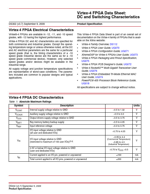
Table 1: Absolute Maximum Ratings
Symbol
Description
VCCINT VCCAUX VCCO VBATT
VREF
Internal supply voltage relative to GND Auxiliary supply voltage relative to GND Output drivers supply voltage relative to GND Key memory battery backup supply Input reference voltage I/O input voltage relative to GND (all user and dedicated I/Os)
-12
-11
-10
1.83
1.96
2.13
1.90
2.04
2.22
1.75
1.87
2.03
1.89
2.03
2.21
1.85
1.98
2.161.801. Nhomakorabea32.09
1.77
1.89
2.06
2.09
2.25
2.46
2.07
2.24
2.45
TIOTP Speed Grade
FPGA可编程逻辑器件芯片XQ4VLX60-10FF68M中文规格书

CarryIn Input Register
The CarryIn input register from fabric is not supported (that is, the attribute CARRYINREG = 1). Workaround Use the CLB register to replace the CarryIn input register, and set attribute CARRYINREG = 0.
CONFIG STEPPING = "1";
EN002 (v1.2) February 5, 2006 Errata Notification
Virtex-4 XC4VLX60CES Errata
Notes and Recommendations (JTAG ID = 2, 3)
Virtex-II and Virtex-II Pro FPGA Designers
The JTAG INTEST instruction outlined in the Virtex-4 Configuration Guide is not supported.
JTAG TDO Output
The JTAG TDO output will 3-state on the rising edge of TCK when the JTAG TAP state machine exits the Shift-DR or Shift-IR states. In the event that the last bit shifted out is a "0," the value might be read as a "1" by the next device in the chain if it has a long hold-time requirement on its TDI pin. Workaround Provide negative skew on TCK between the Virtex-4 device and the next device in the chain. Refer to answer record 19865.
FPGA可编程逻辑器件芯片XC4VLX60-10FF668C中文规格书
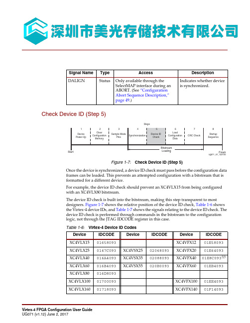
Check Device ID (Step 5)Once the device is synchronized, a device ID check must pass before the configuration data frames can be loaded. This prevents an attempted configuration with a bitstream that is formatted for a different device.For example, the device ID check should prevent an XC4VLX15 from being configured with an XC4VLX80 bitstream.The device ID check is built into the bitstream, making this step transparent to most designers. Figure 1-7 shows the relative position of the device ID check, Table 1-6 shows the Virtex-4 device IDs, and Table 1-7 shows the signals relating to the device ID check. The device ID check is performed through commands in the bitstream to the configuration logic, not through the JTAG IDCODE register in this case.Signal Name Type AccessDescription DALIGNStatusOnly available through the SelectMAP interface during an ABORT. (See “Configuration Abort Sequence Description,” page 49.)Indicates whether device is synchronized.Figure 1-7:Check Device ID (Step 5)Table 1-6:Virtex-4 Device ID CodesDevice IDCODE DeviceIDCODEDevice IDCODE XC4VLX1501658093XC4VFX1201E58093XC4VLX250167C093XC4VSX2502068093XC4VFX2001E64093XC4VLX40016A4093XC4VSX3502088093XC4VFX4001E8C093(1)XC4VLX60016B4093XC4VSX55020B0093XC4VFX6001EB4093XC4VLX80016D8093XC4VLX10001700093XC4VFX10001EE4093XC4VLX16001718093XC4VFX14001F14093Serial Configuration InterfaceClocking Serial Configuration DataFigure2-2 shows how configuration data are clocked into Virtex-4 devices in Slave serialand Master serial modes.Figure 2-2:Serial Daisy Chain Configuration Clocking Sequence Notes relevant to Figure2-2:1.In Figure2-2, bit 0 represents the MSB of the first byte. For example, if the first byte is0xAA (1010_1010), bit 0=1, bit 1=0, bit 2=1, etc.2.For Master configuration mode, CCLK does not transition until after MODE pins aresampled, as indicated by the arrow.LK can be free-running in Slave serial mode.Master Serial ConfigurationThe Master serial mode is designed so that the FPGA can be configured from aXilinx®serial configuration PROM, as shown in Figure2-3.Figure 2-3:Master Serial Mode ConfigurationChapter 2:Configuration InterfacesSlave Serial ConfigurationSlave serial configuration is typically used for devices in a serial daisy chain, or whenconfiguring a single device from an external microprocessor or CPLD. Designconsiderations are similar to Master serial configuration except for the direction of CCLK.A single device in Slave serial mode cannot simply be connected to a PROM, becauseCCLK is an input on both devices.Serial Daisy ChainsMultiple Virtex-4 devices can be configured from a single configuration source byarranging the devices in a serial daisy chain. In a serial daisy chain, devices receive theirconfiguration data through their DIN pin, passing configuration data along todownstream devices through their DOUT pin. The device closest to the configuration datasource is considered the most upstream device, while the device furthest from theconfiguration data source is considered the most downstream device.In a serial daisy chain, the configuration clock is typically provided by the most upstreamdevice in Master serial mode. All other devices are set for Slave serial mode. Figure2-4illustrates this configuration.Alternatively, if a CPLD or microprocessor is used as a configuration controller, all devicescan be set for Slave serial mode. (See “Configuring a Serial Daisy Chain with aMicroprocessor or CPLD,” page 32.)Table 2-4:Virtex-4 SelectMAP Configuration Interface PinsPin NameTypeDedicated or Dual-PurposeDescriptionM[2:0]Input Dedicated MODE pins - determines configuration mode CCLKInput and OutputDedicatedConfiguration clock source for all configuration modes except JTAGSelectMAP Data Three-State Bidirectional Dual PurposeByte-wide (SelectMAP 8 bit) configuration and readback data bus, clocked on rising edge ofCCLK. D0 is the most-significant bit (MSB), D7 the least-significant bit (LSB). In SelectMAP 32 bit, configuring the data order is straight D0=LSB and D31=MSB.(1)Table 2-5:ABORT Status WordBit Number Status Bit Name MeaningD7CFGERR_B Configuration error (active Low)0 = A configuration error has occurred.1 = No configuration error.D6DALIGN Sync word received (active High)0 = No sync word received.1 = Sync word received by interface logic.D5RIP Readback in progress (active High)0 = No readback in progress.1 = A readback is in progress.D4IN_ABORT_B ABORT in progress (active Low)0 = Abort is in progress.1 = No abort in progress.D3-D01111。
FPGA可编程逻辑器件芯片XC4VLX160-10FF1148I中文规格书

XC4010XL-2PQ100C XC4010XL-2PQ100I XC4010XL-2PQ208C XC4010XL-2PQ208I XC4010XL-2TQ144C XC4010XL-2TQ144I XC4010XL-3BG256C XC4010XL-3BG256I XC4010XL-3PQ100C
Description
As part of Xilinx regular product pruning activities, the following XC3000, XC4000XL, XC5206, Virtex, Spartan-3, and Aerospace & Defense “XQ” products have been identified for obsolescence.
XCN08011 (v1.2) April 27, 2010
Байду номын сангаас
Product Discontinuation Notice
Table 9: Virtex-E SCD Part Numbers Affected
Part Number
Replacement Part
XCV1000E-6BG560I0773 XCV1000E-6FG1156C0773 XCV1000E-6FG900C0773 XCV1000E-8FG1156C0773 XCV100E-6BG352I0773 XCV100E-6PQ240C0773 XCV100E-7PQ240C0773 XCV100E-8PQ240C0773 XCV2000E-6BG560C0773 XCV2000E-6BG560I0773 XCV2000E-8BG560C0773 XCV2000E-8FG1156C0773 XCV2000E-8FG680C0773 XCV200E-6BG352C0773 XCV200E-6FG456C0773 XCV200E-6FG456I0773 XCV200E-6PQ240C0773 XCV200E-7BG352C0773 XCV200E-7PQ240C0773 XCV200E-8FG256C0773 XCV200E-8PQ240C0773
FPGA可编程逻辑器件芯片XC4VLX60-12FFG1148C中文规格书
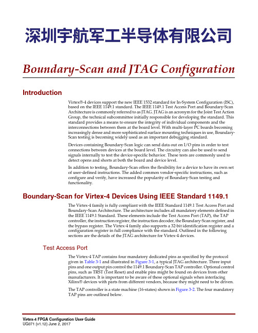
Boundary-Scan and JTAG ConfigurationIntroductionVirtex®-4 devices support the new IEEE 1532 standard for In-System Configuration (ISC),based on the IEEE 1149.1 standard. The IEEE 1149.1 Test Access Port and Boundary-ScanArchitecture is commonly referred to as JTAG. JTAG is an acronym for the Joint Test ActionGroup, the technical subcommittee initially responsible for developing the standard. Thisstandard provides a means to ensure the integrity of individual components and theinterconnections between them at the board level. With multi-layer PC boards becomingincreasingly dense and more sophisticated surface mounting techniques in use, Boundary-Scan testing is becoming widely used as an important debugging standard.Devices containing Boundary-Scan logic can send data out on I/O pins in order to testconnections between devices at the board level. The circuitry can also be used to sendsignals internally to test the device-specific behavior. These tests are commonly used todetect opens and shorts at both the board and device level.In addition to testing, Boundary-Scan offers the flexibility for a device to have its own setof user-defined instructions. The added common vendor-specific instructions, such asconfigure and verify, have increased the popularity of Boundary-Scan testing andfunctionality.Boundary-Scan for Virtex-4 Devices Using IEEE Standard 1149.1 The Virtex-4 family is fully compliant with the IEEE Standard 1149.1 Test Access Port andBoundary-Scan Architecture. The architecture includes all mandatory elements defined inthe IEEE 1149.1 Standard. These elements include the Test Access Port (TAP), the TAPcontroller, the instruction register, the instruction decoder, the Boundary-Scan register, andthe bypass register. The Virtex-4 family also supports a 32-bit identification register and aconfiguration register in full compliance with the standard. Outlined in the followingsections are the details of the JTAG architecture for Virtex-4 devices.Test Access PortThe Virtex-4 TAP contains four mandatory dedicated pins as specified by the protocolgiven in Table3-1 and illustrated in Figure3-1, a typical JTAG architecture. Three inputpins and one output pin control the 1149.1 Boundary-Scan TAP controller. Optional controlpins, such as TRST (Test Reset) and enable pins might be found on devices from othermanufacturers. It is important to be aware of these optional signals when interfacingXilinx®devices with parts from different vendors, because they might need to be driven.The TAP controller is a state machine (16-states) shown in Figure3-2. The four mandatoryTAP pins are outlined below.Table 3-3:Virtex-4 Boundary-Scan InstructionsBoundary-Scan Command Binary Code(9:0)DescriptionEXTEST1111000000Enables Boundary-Scan EXTEST operationSAMPLE1111000001Enables Boundary-Scan SAMPLE operationUSER11111000010Access user-defined register 1USER21111000011Access user-defined register 2USER31111100010Access user-defined register 3USER41111100011Access user-defined register 4CFG_OUT1111000100Access the configuration bus for readbackCFG_IN1111000101Access the configuration bus for configurationINTEST1111000111Enables Boundary-Scan INTEST operationUSERCODE1111001000Enables shifting out user codeIDCODE1111001001Enables shifting out of ID codeHIGHZ11110010103-state output pins while enabling Bypass RegisterJPROGRAM1111001011Equivalent to and has the same affect as PROGRAMJSTART1111001100Clocks the start-up sequence when StartClk is TCK JSHUTDOWN1111001101Clocks the shutdown sequenceISC_ENABLE1111010000Marks the beginning of ISC configuration. Full shutdown is executed ISC_PROGRAM1111010001Enables in-system programmingISC_PROGRAM_SECURITY1111010010Change security status from secure to non-secure mode and vice versa ISC_ADDRESS_SHIFT1111010011For programming, key address is shifted first, before the keyISC_NOOP1111010100No operationISC_READ1111010101Used to read back BBRISC_DISABLE1111010111Completes ISC configuration. Startup sequence is executed BYPASS1111111111Enables BYPASSRESERVED All other codes Xilinx reserved instructionsNotes:1.For FX devices with two processors, the instruction codes are MSB extended with 1s. For example, the CFG_IN instruction is11111111000101.TDI→IR[9:6]IR[5]IR[4]IR[3]IR[2]IR[1:0]→TDO Reserved DONE INIT ISC_ENABLED ISC_DONE0 1Figure 3-4:Virtex-4 Instruction Capture Values Loaded into IR as Part of an Instruction Scan SequenceDevice IDCODE Device IDCODE Device IDCODE XC4VLX1501658093XC4VFX1201E58093 XC4VLX250167C093XC4VSX2502068093XC4VFX2001E64093 XC4VLX40016A4093XC4VSX3502088093XC4VFX4001E8C093(1) XC4VLX60016B4093XC4VSX55020B0093XC4VFX6001EB4093 XC4VLX80016D8093XC4VLX10001700093XC4VFX10001EE4093 XC4VLX16001718093XC4VFX14001F14093 XC4VLX20001734093Chapter 3:Boundary-Scan and JTAG ConfigurationTable 3-5:Example JTAG IDCODE Concatenation (Continued)vvvv ffff fffa aaaa aaaa cccc cccc ccc1hex<v>1E64093 XC4VFX40(1)bin<vvvv>0001111010010100000010010011hex<v>1E8C093 XC4VFX60bin<vvvv>0001111010110100000010010011hex<v>1E B4093 XC4VFX100bin<vvvv>0001111011100100000010010011hex<v>1E E4093 XC4VFX140bin<vvvv>0001111100010100000010010011hex<v>1F14093Boundary-Scan for Virtex-4 Devices Using IEEE Standard 1149.1Single Device ConfigurationTable3-6 describes the TAP controller commands required to configure a Virtex-4 device. Refer to Figure3-2 for TAP controller states. These TAP controller commands are issued automatically if configuring the part with the iMPACT software.。
FPGA可编程逻辑器件芯片EP4SGX360KF43C4中文规格书

Configuring Stratix II and Stratix II GX Devices Data is continuously clocked into the target device until CONF_DONE goes high. The CONF_DONE pin goes high one byte early in parallel configuration (FPP and PPA) modes. The last byte is required for serial configuration (AS and PS) modes. After the device has received the next to last byte of the configuration data successfully, it releases theopen-drain CONF_DONE pin, which is pulled high by an external 10-kΩpull-up resistor. A low-to-high transition on CONF_DONE indicates configuration is complete and initialization of the device can begin. The CONF_DONE pin must have an external 10-kΩ pull-up resistor in order for the device to initialize.In Stratix II and Stratix II GX devices, the initialization clock source is either the internal oscillator (typically 10MHz) or the optional CLKUSR pin. By default, the internal oscillator is the clock source for initialization. If the internal oscillator is used, the Stratix II or Stratix II GX device provides itself with enough clock cycles for proper initialization. Therefore, if the internal oscillator is the initialization clock source, sending the entire configuration file to the device is sufficient to configure and initialize the device. Driving DCLK to the device after configuration is complete does not affect device operation.You can also synchronize initialization of multiple devices or to delay initialization with the CLKUSR option. The Enable user-supplied start-up clock (CLKUSR) option can be turned on in the Quartus II software from the General tab of the Device & Pin Options dialog box. Supplying a clock on CLKUSR does not affect the configuration process. TheCONF_DONE pin goes high one byte early in parallel configuration (FPP and PPA) modes. The last byte is required for serial configuration (AS and PS) modes. After the CONF_DONE pin transitions high, CLKUSR is enabled after the time specified as t CD2CU. After this time period elapses, Stratix II and Stratix II GX devices require 299 clock cycles to initialize properly and enter user mode. Stratix II and Stratix II GX devices support a CLKUSR f MAX of 100MHz.An optional INIT_DONE pin is available, which signals the end of initialization and the start of user-mode with a low-to-high transition. This Enable INIT_DONE Output option is available in the Quartus II software from the General tab of the Device & Pin Options dialog box. If the INIT_DONE pin is used, it is high because of an external 10-kΩpull-up resistor when nCONFIG is low and during the beginning of configuration. Once the option bit to enable INIT_DONE is programmed into the device (during the first frame of configuration data), theINIT_DONE pin goes low. When initialization is complete, theINIT_DONE pin is released and pulled high. The MAX II device must be able to detect this low-to-high transition, which signals the device hasStratix II Device Handbook, Volume2Fast Passive Parallel Configurationentered user mode. When initialization is complete, the device enters usermode. In user-mode, the user I/O pins no longer have weak pull-upresistors and function as assigned in your design.To ensure DCLK and DATA[7..0] are not left floating at the end ofconfiguration, the MAX II device must drive them either high or low,whichever is convenient on your board. The DATA[7..0] pins areavailable as user I/O pins after configuration. When you select the FPPscheme in the Quartus II software, as a default, these I/O pins aretri-stated in user mode. To change this default option in the Quartus IIsoftware, select the Pins tab of the Device & Pin Options dialog box.The configuration clock (DCLK) speed must be below the specifiedfrequency to ensure correct configuration. No maximum DCLK periodexists, which means you can pause configuration by halting DCLK for anindefinite amount of time.1If you are using the Stratix II or Stratix II GX decompressionand/or design security feature and need to stop DCLK, it canonly be stopped three clock cycles after the last data byte waslatched into the Stratix II or Stratix II GX device.By stopping DCLK, the configuration circuit allows enough clock cycles toprocess the last byte of latched configuration data. When the clockrestarts, the MAX II device must provide data on the DATA[7..0] pinsprior to sending the first DCLK rising edge.If an error occurs during configuration, the device drives its nSTATUS pinlow, resetting itself internally. The low signal on the nSTATUS pin alsoalerts the MAX II device that there is an error. If the Auto-restartconfiguration after error option (available in the Quartus II softwarefrom the General tab of the Device & Pin Options (dialog box) is turnedon, the device releases nSTATUS after a reset time-out period (maximumof 100µs). After nSTATUS is released and pulled high by a pull-upresistor, the MAX II device can try to reconfigure the target devicewithout needing to pulse nCONFIG low. If this option is turned off, theMAX II device must generate a low-to-high transition (with a low pulseof at least 2µs) on nCONFIG to restart the configuration process.The MAX II device can also monitor the CONF_DONE and INIT_DONEpins to ensure successful configuration. The CONF_DONE pin must bemonitored by the MAX II device to detect errors and determine whenprogramming completes. If all configuration data is sent, but theCONF_DONE or INIT_DONE signals have not gone high, the MAX IIdevice will reconfigure the target device.Stratix II Device Handbook, Volume2Configuring Stratix II and Stratix II GX Devices1If the optional CLKUSR pin is used and nCONFIG is pulled lowto restart configuration during device initialization, you need toensure CLKUSR continues toggling during the time nSTATUS islow (maximum of 100µs).When the device is in user-mode, initiating a reconfiguration is done bytransitioning the nCONFIG pin low-to-high. The nCONFIG pin should below for at least 2µs. When nCONFIG is pulled low, the device also pullsnSTATUS and CONF_DONE low and all I/O pins are tri-stated. OncenCONFIG returns to a logic high level and nSTATUS is released by thedevice, reconfiguration begins.Figure7–4 shows how to configure multiple devices using a MAX IIdevice. This circuit is similar to the FPP configuration circuit for a singledevice, except the Stratix II or Stratix II GX devices are cascaded formulti-device configuration.Figure7–4.Multi-Device FPP Configuration Using an External HostNote to Figure7–4:(1)The pull-up resistor should be connected to a supply that provides an acceptable input signal for all devices in thechain. V CC should be high enough to meet the V IH specification of the I/O standard on the device and the external host.In multi-device FPP configuration, the first device’s nCE pin is connectedto GND while its nCEO pin is connected to nCE of the next device in thechain. The last device’s nCE input comes from the previous device, whileits nCEO pin is left floating. After the first device completes configurationin a multi-device configuration chain, its nCEO pin drives low to activatethe second device’s nCE pin, which prompts the second device to beginconfiguration. The second device in the chain begins configuration withinone clock cycle; therefore, the transfer of data destinations is transparentto the MAX II device. All other configuration pins (nCONFIG, nSTATUS,DCLK, DATA[7..0], and CONF_DONE) are connected to every device inStratix II Device Handbook, Volume2。
FPGA可编程逻辑器件芯片XC4VLX40-10FF1148I中文规格书
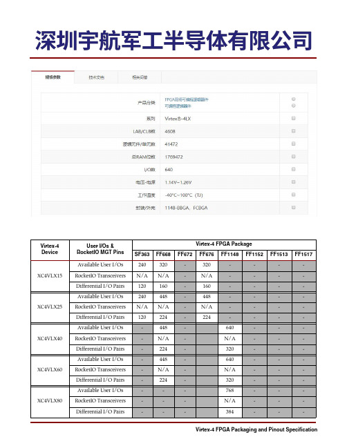
Virtex-4 Device
User I/Os & RocketIO MGT Pins
Virtex-4 FPGA Package SF363 FF668 FF672 FF676 FF1148 FF1152 FF1513 FF1517
Available User I/Os
-
-
-
-
576
-
768
XC4VFX100 RocketIO Transceivers
D9
2
IO_L1P_D15_CC_LC_2
V16
2
IO_L1N_D14_CC_LC_2
V15
2
IO_L2P_D13_LC_2
V6
2
IO_L2N_D12_LC_2
V5
2
IO_L3P_D11_LC_2
T14
2
IO_L3N_D10_LC_2
U13
2
IO_L4P_D9_LC_2
U8
2
IO_L4N_D8_VREF_LC_2
1
IO_L5P_D23_LC_1
D13
1
IO_L5N_D22_LC_1
C13
1
IO_L6P_D21_LC_1
C8
1
IO_L6N_D20_LC_1
D8
1
IO_L7P_D19_LC_1
D12
1
IO_L7N_D18_LC_1
C12
1
IO_L8P_D17_CC_LC_1
C9
1
IO_L8N_D16_CC_LC_1
Virtex-4 Device XC4VLX15
XC4VLX25
XC4VLX40
XC4VLX60
FPGA可编程逻辑器件芯片XC4VLX40-11FF1148I中文规格书

Output Delay MeasurementsOutput delays are measured using a T ektronix P6245TDS500/600 probe (<1pF) across approximately 4 inches of FR4 microstrip trace. Standard termination was used for all testing. The propagation delay of the 4 inch trace is char-acterized separately and subtracted from the final measure-ment, and is therefore not included in the generalized test setup shown in Figure 4.Measurements and test conditions are reflected in the IBIS models except where the IBIS format precludes it. Parame-ters V REF , R REF , C REF , and V MEAS fully describe the test conditions for each I/O standard. The most accurate predic-tion of propagation delay in any given application can be obtained through IBIS simulation, using the following method:1.Simulate the output driver of choice into the generalizedtest setup, using values from T able 31.2.Record the time to V MEAS .3.Simulate the output driver of choice into the actual PCBtrace and load, using the appropriate IBIS model or capacitance value to represent the load.4.Record the time to V MEAS .pare the results of steps 2 and 4. The increase ordecrease in delay yields the actual worst-casepropagation delay (clock-to-input) of the PCB trace.DescriptionI/O Standard AttributeR REF (Ω)C REF (1)(pF)V MEAS(V)V REF (V)LVTTL (Low-Voltage T ransistor-T ransistor Logic)LVTTL (all)1M 0 1.40LVCMOS (Low-Voltage CMOS), 3.3V LVCMOS331M 0 1.650LVCMOS, 2.5V LVCMOS251M 0 1.250LVCMOS, 1.8V LVCMOS181M 00.90LVCMOS, 1.5V LVCMOS151M 00.750LVCMOS, 1.2VLVCMOS121M 00.750PCI (Peripheral Component Interface), 33 MHz, 3.3V PCI33_3 (rising edge)2510(2)0.940PCI33_3 (falling edge)2510(2) 2.03 3.3PCI, 66 MHz, 3.3V PCI66_3 (rising edge)2510(2)0.940PCI66_3 (falling edge)2510(2) 2.03 3.3PCI-X, 133 MHz, 3.3VPCIX (rising edge)2510(3)0.94PCIX (falling edge 2510(3) 2.03 3.3GTL (Gunning T ransceiver Logic)GTL 2500.8 1.2GTL PlusGTLP 250 1.0 1.5HSTL (High-Speed Transceiver Logic), Class I HSTL_I 500V REF 0.75HSTL, Class II HSTL_II 250V REF 0.75HSTL, Class III HSTL_III 5000.9 1.5HSTL, Class IV HSTL_IV 2500.9 1.5HSTL, Class I, 1.8V HSTL_I_18500V REF 0.9HSTL, Class II, 1.8V HSTL_II_1825V REF0.9HSTL, Class III, 1.8VHSTL_III_18500 1.1 1.8CLB Switching Characteristics Table 37: CLB Switching CharacteristicsSymbol DescriptionSpeed GradeUnits -12-11-10XC4VFX(2)XC4VLX/SX ALL DEVICESCombinatorial DelaysT ILO4-input function: F/G inputs to X/Y outputs0.150.150.170.20ns, Max T IF55-input function: F/G inputs to F5 output0.360.350.400.46ns, Max T IF5X5-input function: F/G inputs to X output0.440.430.490.57ns, Max T IF6Y FXINA or FXINB inputs to YMUX output0.300.300.340.39ns, Max T INAFX FXINA input to FX output via MUXFX0.210.210.230.27ns, Max T INBFX FXINB input to FX output via MUXFX0.210.200.230.26ns, Max T BXX BX input to XMUX output0.590.580.650.76ns, Max T BYY BY input to YMUX output0.430.430.480.56ns, Max T BXCY BX input to C OUT output – Getting into carry chain(3)0.600.590.660.78ns, Max T BYCY BY input to C OUT output – Getting into carry chain(3)0.490.480.540.63ns, Max T BYP C IN input to C OUT output – Carry chain delay(3)0.070.070.080.09ns, Max T OPCYF F input to C OUT output – Getting out from carry chain(3)0.450.440.500.58ns, Max T OPCYG G input to C OUT output – Getting out from carry chain(3)0.440.430.480.57ns, Max Sequential DelaysT CKO FF Clock CLK to XQ/YQ outputs0.280.280.310.36ns, Max T CKLO Latch Clock CLK to XQ/YQ outputs0.370.360.410.48ns, Max Setup and Hold Times of CLB Flip-Flops Before/After Clock CLKT DICK/T CKDIBX/BY inputs0.36–0.090.36–0.090.40–0.090.47–0.09ns, MinT CECK/T CKCECE input0.58–0.160.57–0.160.64–0.160.75–0.16ns, MinT FXCK/T CKFXFXINA/FXINB inputs0.42–0.140.41–0.140.46–0.140.54–0.14ns, MinT SRCK/T CKSRSR/BY inputs (synchronous)1.04–0.741.02–0.731.15–0.731.35–0.73ns, MinT CINCK/T CKCINC IN Data Inputs (DI) – Getting out from carry chain(3)0.52–0.230.51–0.230.57–0.230.67–0.23ns, MinSet/ResetT RPW Minimum Pulse Width, SR/BY inputs0.540.530.590.70ns, Min T RQ Delay from SR/BY inputs to XQ/YQ outputs(asynchronous)1.05 1.03 1.15 1.35ns, MaxF TOG Toggle Frequency (MHz) (for export control)118112051205(4)1028MHz Notes:1. A Zero “0” Hold Time listing indicates no hold time or a negative hold time. Negative values cannot be guaranteed “best-case,” but if a “0” is listed,there is no positive hold time.2.The values in this column apply to all XC4VFX -12 parts except XC4VFX12 -12. For XC4VFX12 -12 values, use the values in the adjacent 4VLX/SX-12 column.3.These items are of interest for Carry Chain applications.4.XC4VFX -11 devices are 1181MHz.CLB Distributed RAM Switching Characteristics (SLICEM Only)Table 38: CLB Distributed RAM Switching CharacteristicsSymbolDescription Speed Grade Units-12-11-10XC4VFX (2)XC4VLX/SX ALL DEVICESSequential Delays T SHCKO Clock CLK to X outputs (WE active)(3) 1.61 1.58 1.77 2.08ns, Max T SHCKOF5Clock CLK to F5 output (WE active)1.53 1.50 1.69 1.98ns, MaxSetup and Hold Times Before/After Clock CLK T DS /T DH BX/BY data inputs (DI) 1.26–0.90 1.23–0.88 1.46–0.88 1.80–0.88ns, Min T AS /T AH F/G address inputs 0.88–0.370.86–0.370.97–0.34 1.13–0.29ns, Min T WS /T WH WE input (SR)1.10–0.48 1.08–0.47 1.21–0.47 1.42–0.47ns, MinClock CLK T WPH Minimum Pulse Width, High 0.530.520.590.69ns, Min T WPL Minimum Pulse Width, Low0.550.540.600.70ns, Min T WCMinimum clock period to meet address write cycle time0.760.740.840.98ns, MinCLKOUT_FREQ_FX_HF_MS_MINCLKFX, CLKFX180210210210MHz CLKOUT_FREQ_FX_HF_MS_MAX 350315300MHzInput Clocks (High Frequency Mode)CLKIN_FREQ_DLL_HF_MS_MIN (6)CLKIN (using DLL outputs only)(1,3,4,5)150150150MHz CLKIN_FREQ_DLL_HF_MS_MAX 500450400MHz CLKIN_FREQ_FX_HF_MS_MIN CLKIN (using DFS outputs)(2,3,4)505050MHz CLKIN_FREQ_FX_HF_MS_MAX (6)350315300MHz PSCLK_FREQ_HF_MS_MIN PSCLK111KHz PSCLK_FREQ_HF_MS_MAX500450400MHzTable 45: Operating Frequency Ranges for DCM in Maximum Speed (MS) Mode (Continued)SymbolDescriptionSpeed GradeUnits-12-11-10Table 47: Input Clock TolerancesSymbolDescriptionFrequency RangeValue UnitsDuty Cycle Input Tolerance (in %)CLKIN_PSCLK_PULSE_RANGE_1PSCLK only< 1MHz 25-75%CLKIN_PSCLK_PULSE_RANGE_1_50PSCLK and CLKIN 1 – 50MHz (1)25-75%CLKIN_PSCLK_PULSE_RANGE_50_10050 – 100MHz (1)30-70%CLKIN_PSCLK_PULSE_RANGE_100_200100 – 200MHz (1)40-60%CLKIN_PSCLK_PULSE_RANGE_200_400200 – 400MHz (1)45-55%CLKIN_PSCLK_PULSE_RANGE_400>400MHz45-55%。
FPGA可编程逻辑器件芯片XQ4VFX100-10FF1152I中文规格书

• Up to 100% speed improvement over previous generation devices.
500 MHz Integrated Block Memory
• Up to 10 Mb of integrated block memory • Optional pipeline stages for higher performance • Multi-rate FIFO support logic
512
320 5,760 8
4
N/A
N/A
N/A
13 640
XC4VFX12 64 x 24 12,312 5,472
86
32
36 648
4
0
1
2
N/A
9 320
XC4VFX20 64 x 36 19,224 8,544 134
32
68 1,224 4
0
1
2
8
9 320
XC4VFX40 96 x 52 41,904 18,624 291
• Up to 100% speed improvement over previous generation devices.
DS112 (v3.1) August 30, 2010 Product Specification
Virtex-4 Family Overview
• Programmable single-ended or differential (LVDS) operation
• Input block with an optional single data rate (SDR) or double data rate (DDR) register
FPGA可编程逻辑器件芯片XC4VLX60-10FFG1148C中文规格书

The purpose of this notification is to inform Xilinx customers of the discontinuation of certain Virtex®-4 andVirtex®-5 FPGA devices special part numbers only; devices will continue to ship without change to form, fit, or function, but with updated part numbers.DescriptionSince the introduction of Virtex-4 and Virtex-5 FPGA products, Xilinx has qualified both product families in both Toshiba, in Oita, Japan, and UMC in Taiwan, and has been shipping the majority of devices in each product family from UMC. As part of the consolidation effort described in XCN11030, wafer fabrication for all Virtex-4 and Virtex-5 Devices described in this document will be transferred to UMC.As a result of this transfer, certain part numbers, including SCD and Stepping, will be converted into standard part numbers.For these devices, there is no change to the form, fit, or function of the devices themselves. Qualification data is available in the Xilinx reliability report UG116.Products AffectedThe products affected include all Virtex-4 and Virtex-5 part numbers associated with the following associated SCDand stepping: 0641, 0988, 4009, 4013, 4023, 4058, 4094, 4098, 4108, CS1, CS2 part numbers listed in Table 1,Table 2 and Table 3 below.XCN11031 (v1.1) June 9, 2015Product Discontinuation Notice For Virtex-4 and Virtex-5 FPGA SCDs from Toshiba Wafer FabricationXCN11031 (v1.1) June 9, 2015Product Discontinuation Notice For Virtex-4 and Virtex-5 FPGA SCDs from Toshiba Wafer FabricationXCN11031 (v1.1) June 9, 2015Product Discontinuation Notice For Virtex-4 and Virtex-5 FPGA SCDs from Toshiba Wafer FabricationXCN11031 (v1.1) June 9, 2015Product Discontinuation Notice For Virtex-4 and Virtex-5 FPGA SCDs from Toshiba Wafer FabricationXCN11031 (v1.1) June 9, 2015。
FPGA可编程逻辑器件芯片XQ4VSX55-10CF1148M中文规格书
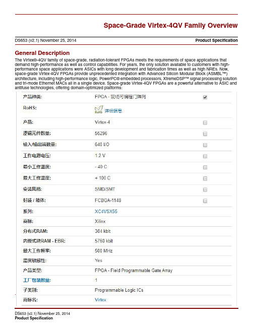
General DescriptionThe Virtex®-4QV family of space-grade, radiation-tolerant FPGAs meets the requirements of space applications that demand high-performance as well as control capabilities. For years, the only solution available to customers with high-performance space applications were ASICs with long development and fabrication times as well as high NREs. Now, space-grade Virtex-4QV FPGAs provide unprecedented integration with Advanced Silicon Modular Block (ASMBL™)architecture, including high-performance logic, PowerPC® embedded processors, XtremeDSP™ signal processing solution and tri-mode Ethernet MACs all in a single device. Space-grade Virtex-4QV FPGAs are a powerful alternative to ASIC and antifuse technologies, offering domain-optimized platforms:Space-Grade Virtex-4QV Family OverviewDS653 (v2.1) November 25, 2014Product SpecificationSystem Blocks Common to all Virtex-4QV Devices400-MHz Xesium Clock Technology•Up to 20 digital clock manager (DCM) modules •Precision clock deskew and phase shift•Flexible frequency synthesis•Dual operating modes to ease performance trade-off decisions•Improved maximum input/output frequency•Improved phase shifting resolution•Reduced output jitter•Low-power operation•Enhanced phase detectors•Wide phase shift range•Companion phase-matched clock divider (PMCD) blocks •Differential clocking structure for optimized low-jitter clocking and precise duty cycle•32 global clock networks•Regional I/O and local clocksFlexible Logic Resources•Up to 40% speed improvement over previous generation devices•Up to 200,000 logic cells including:•Up to 178,176 internal registers with clock enable (XC4VLX200)•Up to 178,176 look-up tables (LUTs)•Logic expanding multiplexers and I/O registers •Cascadable variable shift registers or distributed memory capability•Advanced LUT features (SRL and RAM) can be used in conjunction with configuration scrubbing400-MHz XtremeDSP Slices•Dedicated 18-bit x18-bit multiplier, multiply-accumulator, or multiply-adder blocks•Optional pipeline stages for enhanced performance •Optional 48-bit accumulator for multiply accumulate (MACC) operation•Integrated adder for complex-multiply or multiply-add operation•Cascadable multiply or MACC•Up to 100% speed improvement over previous generation devices.400-MHz Integrated Block Memory•Up to 10 Mb of integrated block memory•Optional pipeline stages for higher performance •Multi-rate FIFO support logic•Full and empty flag support•Fully programmable almost-full and almost-empty flags•Synchronous/asynchronous operation•Dual-port architecture•Independent read and write port width selection (RAM only)•18-Kb blocks (memory and parity/sideband memory support)•Configurations from 16K x1 to 512x36 (4K x4 to 512x36 for FIFO operation)•Byte-write capability (connection to PPC405, etc.)•Dedicated cascade routing to form 32K x1 memory without using FPGA routing•Up to 100% speed improvement over previous generation devices.Virtex-4QV FPGA FeaturesThis section briefly describes the features of the Virtex-4QV family of space-grade FPGAs.Input/Output (SelectIO) BlocksIOBs are programmable and can be categorized as follows:•Programmable single-ended or differential (LVDS) operation.•Input block with an optional single data rate (SDR) or double data rate (DDR) register.•Output block with an optional SDR or DDR register.•Bidirectional block•Per-bit deskew circuitry•Dedicated I/O and regional clocking resources.•Built in data serializer/deserializerThe IOB registers are either edge-triggered D-type flip-flops or level-sensitive latches.IOBs support the following single-ended standards:•LVTTL•LVCMOS (3.3V, 2.5V, 1.8V, and 1.5V)•PCI™ (33 and 66 MHz)•PCI-X™•GTL and GTLP•HSTL 1.5V and 1.8V (Class I, II, III, and IV)•SSTL 1.8V and 2.5V (Class I and II)The DCI I/O feature can be configured to provide on-chip termination for each single-ended I/O standard and some differential I/O standards.The IOB elements also support the following differential signaling I/O standards:•LVDS and Extended LVDS (2.5V only)•BLVDS (Bus LVDS)•ULVDS•HyperTransport™ technology•Differential HSTL 1.5V and 1.8V (Class II)•Differential SSTL 1.8V and 2.5V (Class II)Two adjacent pads are used for each differential pair.Two or four IOB blocks connect to one switch matrix to access the routing resources.Per-bit deskew circuitry allows for programmable signal delay internal to the FPGA. Per-bit deskew flexibly provides fine-grained increments of delay to carefully produce a range of signal delays. This capability is especially useful for synchronizing signal edges in source synchronous interfaces.General-purpose I/O in selected locations (four per bank) are designed to be regional clock capable I/O by adding special hardware connections for I/O in the same locality. These regional clock inputs are distributed within a limited region to minimize clock skew between IOBs. Regional I/O clocking supplements the global clocking resources.Data serializer/deserializer capability is added to every I/O to support source synchronous interfaces. A serial-to-parallel converter with associated clock divider is included in the input path, and a parallel-to-serial converter in the output path.An in-depth guide to the Virtex-4QV FPGA IOB is discussed in UG070, Virtex-4 FPGA User Guide.Configurable Logic Blocks (CLBs)A CLB resource is made up of four slices. Each slice is equivalent and contains:•Two function generators (F and G)•Two storage elements•Arithmetic logic gates•Large multiplexers•Fast carry look-ahead chainThe function generators, F and G, are configurable as4-input look-up tables (LUTs). T wo slices in a CLB can have their LUTs configured as 16-bit shift registers, or as 16-bit distributed RAM. In addition, the two storage elements are either edge-triggered D-type flip-flops or level-sensitive latches.Each CLB has internal fast interconnect and connects to a switch matrix to access general routing resources.The Virtex-4QV FPGA CLBs are further discussed in the Virtex-4FPGA User Guide.Block RAMThe block RAM resources are 18-Kb true dual-port RAM blocks, programmable from 16K x 1 to 512 x 36, in various depth and width configurations. Each port is totally synchronous and independent, offering three read-during-write modes. Block RAM is cascadable to implement large embedded storage blocks.Additionally, back-end pipeline registers, clock control circuitry, built-in FIFO support, and byte write enable are new features supported in the Virtex-4QV FPGA.The block RAM feature in Virtex-4QV devices is further discussed in the Virtex-4 FPGA User Guide.。
FPGA可编程逻辑器件芯片XQ4VLX40-10FF668I中文规格书
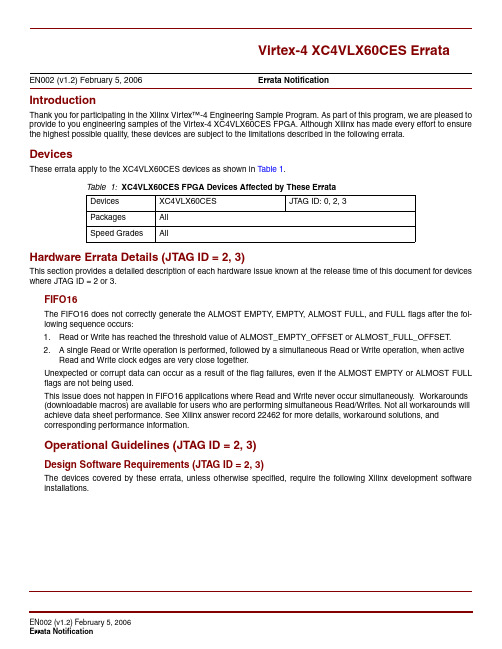
Virtex-4 XC4VLX60CES Errata
Operational Guidelines (JTAG ID = 0)
Design Software Requirements (JTAG ID = 0)
The devices covered by these errata, unless otherwise specified, require the following Xilinx development software installations.
Operational Guidelines (JTAG ID = 2, 3)
Design ware Requirements (JTAG ID = 2, 3)
The devices covered by these errata, unless otherwise specified, require the following Xilinx development software installations.
EN002 (v1.2) February 5, 2006 Errata Notification
Virtex-4 XC4VLX60CES Errata
Notes and Recommendations (JTAG ID = 2, 3)
Virtex-II and Virtex-II Pro FPGA Designers
Packages
All
Speed Grades All
Hardware Errata Details (JTAG ID = 2, 3)
This section provides a detailed description of each hardware issue known at the release time of this document for devices where JTAG ID = 2 or 3.
FPGA可编程逻辑器件芯片XC4VLX80-10FF1148I中文规格书
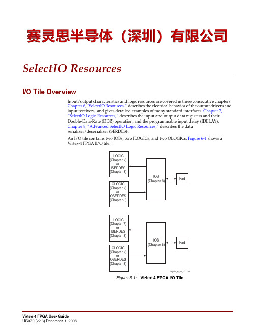
SelectIO ResourcesI/O Tile OverviewInput/output characteristics and logic resources are covered in three consecutive chapters.Chapter6, “SelectIO Resources,” describes the electrical behavior of the output drivers andinput receivers, and gives detailed examples of many standard interfaces. Chapter7,“SelectIO Logic Resources,” describes the input and output data registers and theirDouble-Data-Rate (DDR) operation, and the programmable input delay (IDELAY).Chapter8, “Advanced SelectIO Logic Resources,” describes the dataserializer/deserializer (SERDES).An I/O tile contains two IOBs, two ILOGICs, and two OLOGICs. Figure6-1 shows aVirtex-4 FPGA I/O tile.Figure 6-1:Virtex-4 FPGA I/O TileChapter 5:Configurable Logic Blocks (CLBs)Multiplexer Primitives and SubmodulesFour primitives are available for access to the dedicated MUXFX in each slice. In theexample shown in Table5-16, MUXF7 is available only in slice S2.Table 5-16:MUXFX ResourcesPrimitive Slice Control Input OutputMUXF5S0, S1, S2, S3S I0, I1OMUXF6S0, S1S I0, I1OMUXF7S2S I0, I1OMUXF8S3S I0, I1OChapter 6:SelectIO ResourcesSelectIO Resources IntroductionAll Virtex-4 FPGAs have configurable high-performance SelectIO™ technology driversand receivers, supporting a wide variety of standard interfaces. The robust feature setincludes programmable control of output strength and slew rate, and on-chip terminationusing Digitally Controlled Impedance (DCI). All banks can support 3.3V I/O.Each IOB contains both input, output, and 3-state SelectIO drivers. These drivers can beconfigured to various I/O standards. Differential I/O uses the two IOBs grouped togetherin one tile.•Single-ended I/O standards (LVCMOS, LVTTL, HSTL, SSTL, GTL, PCI)•Differential I/O standards (LVDS, LDT, LVPECL, BLVDS, CSE Differential HSTL andSSTL)Note:Differential and V REF-dependent inputs are powered by V CCAUX.Each Virtex-4 FPGA I/O tile contains two IOBs, and also two ILOGIC blocks and twoOLOGIC blocks, as described in Chapter7, “SelectIO Logic Resources”.Figure6-2 shows the basic IOB and its connections to the internal logic and the device pad.Virtex-4 FPGA I/O Bank RulesThe number of banks available in Virtex-4 devices is not limited to eight as in previousXilinx® architectures. In Virtex-4 devices, with some exceptions in the center column, anI/O bank consists of 64 IOBs (32 CLBs and two clock regions). As a result, the number ofbanks depends upon the device size. In the Virtex-4 Family Overview the total number ofI/O banks is listed by device type. The XC4VLX25 has 10 usable I/O banks and oneconfiguration bank. Figure6-3 is an example of a columnar floorplan showing theXC4VLX25 I/O banks.Figure 6-3:XC4VLX25 I/O Banks3.3V I/O SupportThe Virtex-4 architecture supports 3.3V single-ended I/O standards in all banks.Reference Voltage (V REF) PinsLow-voltage, single-ended I/O standards with a differential amplifier input buffer requirean input reference voltage (V REF). V REF is an external input into Virtex-4 devices. Withineach I/O bank, one of every 16 I/O pins is automatically configured as a V REF input, ifusing a single-ended I/O standard requiring a differential amplifier input buffer.Output Drive Source Voltage (V CCO) PinsMany of the low-voltage I/O standards supported by Virtex-4 devices require a differentoutput drive voltage (V CCO). As a result, each device often supports multiple output drivesource voltages.Output buffers within a given V CCO bank must share the same output drive sourcevoltage. The following input buffers use the V CCO voltage: LVTTL, LVCMOS, PCI, LVDCIand other DCI standards.Controlled Impedance Driver (Source T ermination)Some I/O standards, such as LVCMOS, must have a drive impedance matching thecharacteristic impedance of the driven line. DCI can provide controlled impedance output drivers to eliminate reflections without an external source termination. The impedance is set by the external reference resistors with resistance equal to the trace impedance. The DCI I/O standards supporting the controlled impedance driver are: LVDCI_15, LVDCI_18, LVDCI_25, LVDCI_33, HSLVDCI_15, HSLVDCI_18, HSLVDCI_25, and HSLVDCI_33. Figure 6-4 illustrates a controlled impedance driver in a Virtex-4 device.Controlled Impedance Driver with Half Impedance (Source T ermination)DCI also provides drivers with one half of the impedance of the reference resistors. This doubling of the reference resistor value reduces the static power consumption throughFigure 6-4:Controlled Impedance Driver。
FPGA可编程逻辑器件芯片XQ4YLX60-10FF668M中文规格书
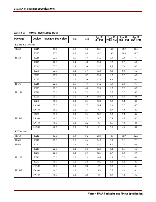
Chapter 5: Thermal Specifications Table 5-1: Thermal Resistance DataPackage Device Package Body SizeθJCθJB θJA @0 LFMθJA @250 LFMθJA @500 LFMθJA @750 LFMLX and SX DevicesSF363LX1517.00.5 5.620.814.712.912.0 LX2517.00.3 4.919.013.511.811.0FF668LX1527.00.6 4.414.29.37.87.1 LX2527.00.4 4.013.48.77.3 6.7LX4027.00.3 3.613.08.57.1 6.5LX6027.00.2 3.412.48.1 6.8 6.2SX2527.00.4 3.913.48.77.3 6.7SX3527.00.2 3.612.78.37.0 6.4FF676LX1527.00.6 4.414.29.37.87.1 LX2527.00.4 4.013.48.77.3 6.7FF1148LX4035.00.3 2.811.0 6.7 5.5 4.9 LX6035.00.2 2.610.6 6.4 5.3 4.8LX8035.00.2 2.410.4 6.3 5.1 4.6LX10035.00.1 2.210.1 6.1 5.0 4.5LX16035.00.1 2.19.7 5.9 4.8 4.3SX5535.00.2 2.410.3 6.3 5.1 4.6FF1513LX10040.00.1 2.39.7 5.8 4.7 4.2 LX16040.00.1 2.29.3 5.6 4.5 4.0LX20040.00.1 2.09.1 5.5 4.4 4.0FX DevicesSF363FX1217.00.5 5.720.814.712.912.0FF668FX1227.00.6 4.414.29.37.87.1FF672FX2027.00.4 3.813.58.77.4 6.8 FX4027.00.2 3.312.68.2 6.9 6.3FX6027.00.1 3.112.07.7 6.5 5.9FF1152FX4035.00.2 2.610.7 6.5 5.3 4.8 FX6035.00.2 2.510.2 6.2 5.1 4.7FX10035.00.1 2.29.9 6.0 4.9 4.4FF1517FX10040.00.1 2.29.5 5.7 4.6 4.1 FX14040.00.1 2.08.6 5.0 4.1 3.7Virtex-4 FPGA Packaging and Pinout SpecificationVirtex-4 FPGA Power Management StrategyVirtex-4 FPGA Packaging and Pinout SpecificationVirtex-4 FPGA Packaging and Pinout SpecificationChapter 5: Thermal Specifications•Heat Sinking Solutions at the System LevelDepending on the system’s physical as well as mechanical constraints, the expectation is that the thermal budget will be maintained with custom or OEM heat sink solutions,providing the third prong in the thermal management strategy. At this point, Xilinx has left the heat sink solution to the system level designers who can tailor the design and solution to the constraints of their systems, being fully aware that the part has certain inherent capabilities for delivering the heat to the surface.The Virtex-4 FPGA packages can be grouped into medium- and high-performance packages based on their power handling capabilities. All Virtex-4 FPGA packages can use thermal enhancements, ranging from simple airflow to schemes that can include passive as well as active heat sinks. This is particularly true for the bigger flip-chip BGA packages where system designers have the option to further enhance the packages with bigger and more elaborate heat sinks to handle excesses of 20 watts with arrangements that consider system physical constraints.Some Thermal Management OptionsThe flip-chip thermal management chart in Figure 5-2 illustrates simple but incremental power management schemes that can be applied on a flip-chip BGA package.•For moderate power dissipation (less than 6 watts), the use of passive heat sinks and heat spreaders attached with thermally conductive double-sided tapes or retainers (with TIM around 0.2•C/watt) can offer quick thermal solutions in these packages.•The use of lightweight, finned, external, passive heat sinks can be effective fordissipating up to 10 - 20 watts in the bigger packages. The more efficient external heat sinks tend to be tall and heavy. To help protect component joints from heat sinkinduced stress cracks, the use of spring-loaded pins or clips that transfer the mounting stress to a circuit board is advisable whenever a bulky heat sink is considered. The diagonals of some of these heat sinks may be designed with extensions to allow direct connection to the board.•As stated earlier, the flip-chip BGA packages offered for Virtex-4 devices are thermally enhanced BGAs with the die facing down. These packages have an exposed metal heat sink at the top. These high-end thermal packages lend themselves to theapplication of efficient external heat sinks (passive or active) for further heat removal efficiency. Again, precautions must be taken to prevent component damage when aFigure 5-2:Thermal Management Options for Flip-Chip BGA PackagesSupport for Compact Thermal Models (CTM)Virtex-4 FPGA Packaging and Pinout SpecificationVirtex-4 FPGA Packaging and Pinout Specification UG075 (v3.3)September 19, 2008Chapter 5:Thermal Specifications。
FPGA可编程逻辑器件芯片XQ4VLX160-10FF148I中文规格书
Reset to Ready for IDELAYCTRL (Maximum) REFCLK frequency REFCLK precision
TIDELAYCTRL_RPW TIDELAYPAT_JIT
Minimum Reset pulse width
Pattern dependent period jitter in delay chain for clock pattern
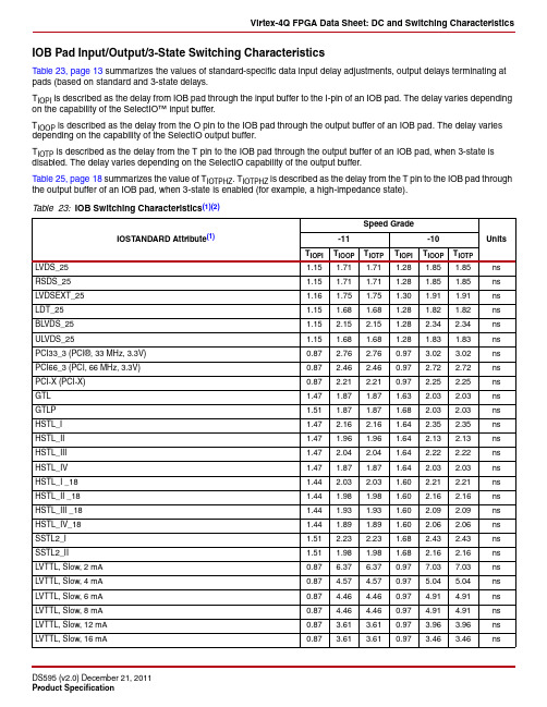
TIOTP 1.85 1.85 1.91 1.82 2.34 1.83 3.02 2.72 2.25 2.03 2.03 2.35 2.13 2.22 2.03 2.21 2.16 2.09 2.06 2.43 2.16 7.03 5.04 4.91 4.91 3.96 3.46
Units
ns ns ns ns ns ns ns ns ns ns ns ns ns ns ns ns ns ns ns ns ns ns ns ns ns ns ns
TIOOP is described as the delay from the O pin to the IOB pad through the output buffer of an IOB pad. The delay varies depending on the capability of the SelectIO output buffer.
FPGA可编程逻辑器件芯片XQ4VLX60-10FFG1148M中文规格书
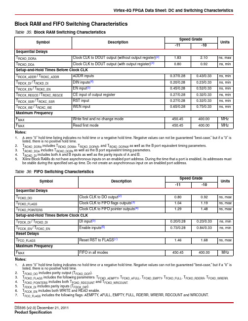
Block RAM and FIFO Switching Characteristics Table 35:Block RAM Switching CharacteristicsSymbol DescriptionSpeed GradeUnits -11-10Sequential DelaysT RCKO_DORA Clock CLK to DOUT output (without output register)(2) 1.83 2.10ns, max T RCKO_DOA Clock CLK to DOUT output (with output register)(3)0.800.92ns, min Setup-and-Hold Times Before Clock CLKT RCCK_ADDR/T RCKC_ADDR ADDR inputs0.37/0.280.43/0.33ns, min T RDCK_DI/T RCKD_DI DIN inputs(4)0.20/0.280.23/0.33ns, min T RCCK_EN/T RCKC_EN EN input(5)0.45/0.280.52/0.33ns, min T RCCK_REGCE/T RCKC_REGCE CE input of output register0.27/0.280.32/0.33ns, min T RCCK_SSR/T RCKC_SSR RST input0.27/0.280.32/0.33ns, min T RCCK_WE/T RCKC_WE WEN input0.65/0.280.75/0.33ns, min Maximum FrequencyF MAX Write first and no change mode450.45400.00MHz F MAX Read first mode450.45400.00MHz Notes:1. A zero “0” hold time listing indicates no hold time or a negative hold time. Negative values can not be guaranteed “best-case,” but if a “0” islisted, there is no positive hold time.2.T RCKO_DORA includes T RCKO_DOWA, T RCKO_DOPAR, and T RCKO_DOPAW as well as the B port equivalent timing parameters.3.T RCKO_DOA includes T RCKO_DOPA as well as the B port equivalent timing parameters.4.T RCKO_DI includes both A and B inputs as well as the parity inputs of A and B.5.Xilinx Block RAMs do not have asynchronous inputs on an enabled port address. During the time that a port is enabled, its addresses mustbe stable during the specified set-up time. Do not create an asynchronous input on an enabled port address.Table 36:FIFO Switching CharacteristicsSymbol DescriptionSpeed GradeUnits -11-10Sequential DelaysT FCKO_DO Clock CLK to DO output(2)0.800.92ns, max T FCKO_FLAGS Clock CLK to FIFO flags outputs(3) 1.04 1.19ns, max T FCKO_POINTERS Clock CLK to FIFO pointer outputs(4) 1.29 1.48ns, max Setup-and-Hold Times Before Clock CLKT FDCK_DI/T FCKD_DI DI input(5)0.20/0.280.23/0.33ns, min T FCCK_EN/T FCKC_EN Enable inputs(6)0.73/0.280.84/0.33ns, min Reset DelaysT FCO_FLAGS Reset RST to FLAGS(7) 1.46 1.68ns, max Maximum FrequencyF MAX FIFO in all modes450.45400.00MHzNotes:1. A zero “0” hold time listing indicates no hold time or a negative hold time. Negative values can not be guaranteed “best-case,” but if a “0” islisted, there is no positive hold time.2.T FCKO_DO includes parity output (T FCKO_DOP).3.T FCKO_FLAGS includes the following parameters: T FCKO_AEMPTY, T FCKO_AFULL, T FCKO_EMPTY, T FCKO_FULL, T FCKO_RDERR, T FCKO_WRERR.4.T FCKO_POINTERS includes both T FCKO_RDCOUNT and T FCKO_WRCOUNT.5.T FDCK_DI includes parity inputs (T FDCK_DIP).6.T FCCK_EN includes both WRITE and READ enable.7.T FCO_FLAGS includes the following flags: AEMPTY, AFULL, EMPTY, FULL, RDERR, WRERR, RDCOUNT and WRCOUNT.System-Synchronous Switching CharacteristicsVirtex-4Q Pin-to-Pin Output Parameter GuidelinesAll devices are 100% functionally tested. The representative values for typical pin locations and normal clock loading are listed in Table50. Values are expressed in nanoseconds unless otherwise noted.Table 50:Global Clock Input-to-Output Delay for LVCMOS25, 12mA, Fast Slew Rate, With DCMSymbol Description DeviceSpeed GradeUnits -11-10I-Grade I-Grade M-GradeLVCMOS25 Global Clock Input-to-Output Delay using Output Flip-Flop, 12mA, Fast Slew Rate, with DCM.T ICKOFDCM Global Clock and OFF with DCMXQ4VLX25–– 3.36ns XQ4VLX40– 3.32 3.42ns XQ4VLX60– 3.45 3.53ns XQ4VLX80 3.27––ns XQ4VLX100 3.33 3.79–ns XQ4VLX160– 3.82–ns XQ4VSX55– 3.62 4.14ns XQ4VFX60– 3.77 3.96ns XQ4VFX100 3.58––nsNotes:1.Listed above are representative values where one global clock input drives one vertical clock line in each accessible column, and where allaccessible IOB and CLB flip-flops are clocked by the global clock net.2.DCM output jitter is already included in the timing calculation.3.Clock to out has +320 ps offset for operation outside of the industrial temperature range.Table 51:Global Clock Input-to-Output Delay for LVCMOS25, 12mA, Fast Slew Rate, Without DCMSymbol Description DeviceSpeed GradeUnits -11-10I-Grade I-Grade M-GradeLVCMOS25 Global Clock Input-to-Output Delay using Output Flip-Flop, 12mA, Fast Slew Rate, without DCM.T ICKOF Global Clock and OFF without DCM XQ4VLX25––8.34nsXQ4VLX40–8.508.73nsXQ4VLX60–8.708.94nsXQ4VLX807.85––nsXQ4VLX1008.159.18–nsXQ4VLX160–9.46–nsXQ4VSX55–9.009.54nsXQ4VFX60–8.859.11nsXQ4VFX1008.40––nsNotes:1.Listed above are representative values where one global clock input drives one vertical clock line in each accessible column, and where allaccessible IOB and CLB flip-flops are clocked by the global clock net.2.Clock to out has +250 ps offset for operation outside of the industrial temperature range.Symbol Description DeviceSpeed GradeUnits -11-10I-Grade I-Grade M-GradeInput Setup-and-Hold Time Relative to Global Clock Input Signal for LVCMOS25 Standard.(1)T PSDCM/T PHDCM No Delay Global Clock and IFFwith DCM(2)XQ4VLX25–– 1.65/–0.43ns XQ4VLX40– 1.50/–0.46 1.69/–0.46ns XQ4VLX60– 1.55/–0.36 1.71/–0.36ns XQ4VLX80 1.42/–0.21––ns XQ4VLX100 1.48/–0.14 1.56/–0.08–ns XQ4VLX160– 1.89/–0.05–ns XQ4VSX55– 1.55/–0.13 1.73/–0.13ns XQ4VFX60– 1.44/0.09 1.53/0.12ns XQ4VFX100 1.42/0.20––nsSymbol Description DeviceSpeed GradeUnits -11-10I-Grade I-Grade M-GradeExample Data Input Setup-and-hold Times Relative to a Forwarded Clock Input Pin, Using DCM and Global Clock Buffer.(1)(3)T PSDCM_0/T PHDCM_0No Delay Global Clock and IFFwith DCM inSource-Synchronous Mode(2)XQ4VLX25–––0.07/1.09ns XQ4VLX40––0.37/1.19–0.03/1.19ns XQ4VLX60––0.32/1.29–0.11/1.29ns XQ4VLX80–0.38/1.34––ns XQ4VLX100–0.31/1.41–0.31/1.57–ns XQ4VLX160––0.31/1.89–ns XQ4VSX55––0.32/1.52–0.09/1.52ns XQ4VFX60––0.43/1.74–0.25/1.77ns XQ4VFX100–0.38/1.75––nsSymbolDescriptionDevice Package Value Units T PKGSKEWPackage Skew (1)XQ4VLX25SF36390ps FF668110ps XQ4VLX40FF668110ps XQ4VLX60EF668130ps FF668130ps FF1148140ps XQ4VLX80FF1148155ps XQ4VLX100FF1148140ps XQ4VLX160FF1148145ps XQ4VSX55FF1148145ps XQ4VFX60EF672110ps XQ4VFX100FF1152150psNotes:1.These values represent the worst-case skew between any two balls of the package: shortest flight time to longest flight time from pad to ball (7.1ps/mm).2.Package trace length information is available for these device/package combinations. This information can be used to deskew the package.Table 57:Sample WindowSymbolDescriptionDevice Speed Grade Units -11-10T SAMP Sampling Error at Receiver Pins (1)All 500550ps T SAMP_BUFIO Sampling Error at Receiver Pins using BUFIO (2)All400450psNotes:1.This parameter indicates the total sampling error of Virtex-4FPGA DDR input registers across voltage, temperature, and process. The characterization methodology uses the DCM to capture the DDR input registers’ edges of operation. These measurements include:-CLK0 DCM jitter-DCM accuracy (phase offset)-DCM phase shift resolutionThese measurements do not include package or clock tree skew.2.This parameter indicates the total sampling error of Virtex-4FPGA DDR input registers across voltage, temperature, and process. The characterization methodology uses the BUFIO clock network and IDELAY to capture the DDR input registers’ edges of operation. These measurements do not include package or clock tree skew.Symbol DescriptionSpeed Grade Units-11-10Data Input Setup-and-Hold Times Relative to a Forwarded Clock Input Pin Using BUFIO T PSCS /T PHCS Setup/hold of I/O clock across multiple clock regions–0.45/1.08–0.44/1.17nsPin-to-Pin Clock-to-Out Using BUFIOT ICKOFCSClock-to-Out of I/O clock across multiple clock regions4.545.02ns。
FPGA可编程逻辑器件芯片XQR2V6000-4CF1144H中文规格书
Notes: 1. "R" means the bit is not used and reserved for future use.
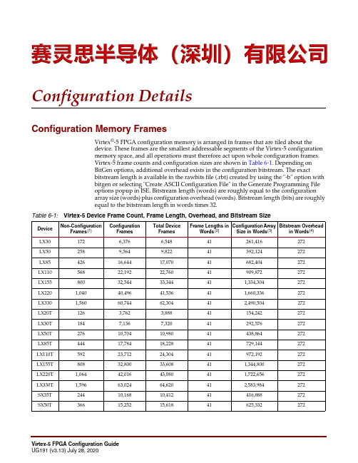
Virtex-5 FPGA Configuration Guide UG191 (v3.13) July 28, 2020
Configuration Registers
Control Register 1 (CTL1)
CTL0 and CTL1 registers are used to configure the Virtex-5 device. This register is reserved.
Reserved
Description
Bit Index Value
696
30,016
30,712
41
1,230,656
272
FX130T
870
37,520
38,390
41
1,538,320
272
FX200T
1,236
54,000
55,236
41
2,214,000
272
TX150T
810
32,980
33,790
41
1,352,180
272
TX240T
1,236
50,112
Type 1 Packet
The Type 1 packet is used for register reads and writes. Only 5 out of 14 register address bits are used in Virtex-5 FPGAs. The header section is always a 32-bit word.
FPGA可编程逻辑器件芯片XQ4VLX100-11FF1148M中文规格书
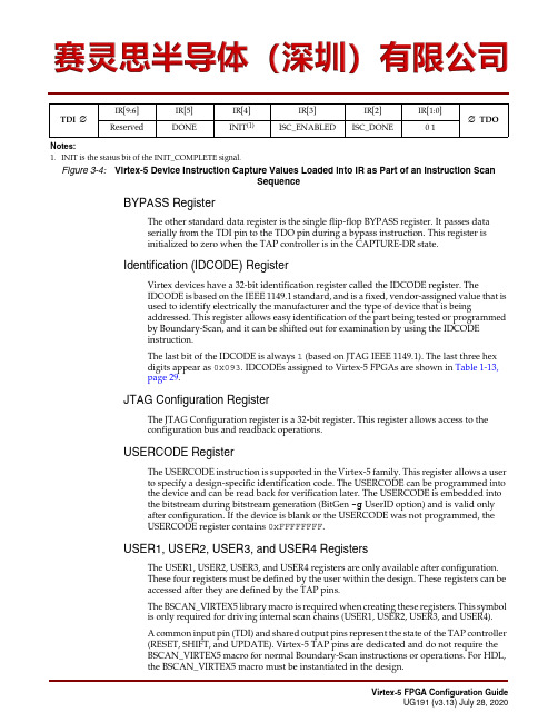
BYPASS RegisterThe other standard data register is the single flip-flop BYPASS register. It passes dataserially from the TDI pin to the TDO pin during a bypass instruction. This register isinitialized to zero when the TAP controller is in the CAPTURE-DR state.Identification (IDCODE) RegisterVirtex devices have a 32-bit identification register called the IDCODE register. TheIDCODE is based on the IEEE 1149.1 standard, and is a fixed, vendor-assigned value that isused to identify electrically the manufacturer and the type of device that is beingaddressed. This register allows easy identification of the part being tested or programmedby Boundary-Scan, and it can be shifted out for examination by using the IDCODEinstruction.The last bit of the IDCODE is always 1 (based on JTAG IEEE 1149.1). The last three hexdigits appear as 0x093. IDCODEs assigned to Virtex-5 FPGAs are shown in Table 1-13,page 29.JTAG Configuration RegisterThe JTAG Configuration register is a 32-bit register. This register allows access to theconfiguration bus and readback operations.USERCODE RegisterThe USERCODE instruction is supported in the Virtex-5 family. This register allows a userto specify a design-specific identification code. The USERCODE can be programmed intothe device and can be read back for verification later. The USERCODE is embedded intothe bitstream during bitstream generation (BitGen -g UserID option) and is valid onlyafter configuration. If the device is blank or the USERCODE was not programmed, theUSERCODE register contains 0xFFFFFFFF .USER1, USER2, USER3, and USER4 RegistersThe USER1, USER2, USER3, and USER4 registers are only available after configuration.These four registers must be defined by the user within the design. These registers can beaccessed after they are defined by the TAP pins.The BSCAN_VIRTEX5 library macro is required when creating these registers. This symbolis only required for driving internal scan chains (USER1, USER2, USER3, and USER4).A common input pin (TDI) and shared output pins represent the state of the TAP controller(RESET, SHIFT, and UPDATE). Virtex-5 TAP pins are dedicated and do not require theBSCAN_VIRTEX5 macro for normal Boundary-Scan instructions or operations. For HDL,the BSCAN_VIRTEX5 macro must be instantiated in the design.TDI ∅IR[9:6]IR[5]IR[4]IR[3]IR[2]IR[1:0]∅TDOReserved DONE INIT (1)ISC_ENABLED ISC_DONE 0 1Notes: 1.INIT is the status bit of the INIT_COMPLETE signal.Figure 3-4:Virtex-5 Device Instruction Capture Values Loaded into IR as Part of an Instruction ScanSequenceChapter 3:Boundary-Scan and JTAG ConfigurationMultiple Device ConfigurationIt is possible to configure multiple Virtex-5 devices in a chain. (See Figure3-7.) The devicesin the JTAG chain are configured one at a time. The multiple device configuration steps canbe applied to any size chain.Refer to the state diagram in Figure3-2 for the following TAP controller steps:1.On power-up, place a logic 1 on the TMS and clock the TCK five times. This ensuresstarting in the TLR (Test-Logic-Reset) state.2.Load the CFG_IN instruction into the target device (and BYPASS in all other devices).Go through the RTI state (RUN-TEST/IDLE).3.Load in the configuration bitstream per step7 through step11 in Table3-4.4.Repeat step2 and step3 for each device.5.Reset all TAPs by clocking five 1s on TMS.6.Load the JSTART command into all devices.7.Go to the RTI state and clock TCK 12 times.All devices are active at this point.JT AG He a derDevice 0Device 1Device 2UG191_c3_01_020609Figure 3-7:Boundary-Scan Chain of DevicesIf JTAG is the only configuration mode, then PROGRAM_B, INIT_B, and DONE can eachbe tied High to separate resistors as shown in the Master serial or Master/Slave SerialMode Daisy Chain Configuration (see Figure2-3 and Figure2-4).Boundary-Scan for Virtex-5 Devices Using IEEE Standard 1149.1Reconfiguring through Boundary-ScanThe ability of Virtex-5 devices to perform partial reconfiguration is the reason that the configuration memory is not cleared when reconfiguring the device. When reconfiguring a chain of devices, refer to step3 in Table3-4. There are two methods to reconfigure Virtex-5 devices without possible internal contention. The first method is to pulse thePROGRAM_B pin, resetting the internal configuration memory. The alternate method is to perform a shutdown sequence, placing the device in a safe state. The following shutdown sequence includes using internal registers. (For details on internal registers, refer toChapter7, “Readback and Configuration Verification.”)1.Load the CFG_IN instruction.2.In the SHIFT-DR state, load the synchronization word followed by the Reset CRCRegister (RCRC) command.1111 1111 1111 1111 1111 1111 1111 1111∅ Dummy word1010 1010 1001 1001 0101 0101 0110 0110∅ Synchronization word0011 0000 0000 0000 1000 0000 0000 0001∅ Header: Write to CMD register0000 0000 0000 0000 0000 0000 0000 0111∅ RCRC command0010 0000 0000 0000 0000 0000 0000 0000∅ NO-OP0000 0000 0000 0000 0000 0000 0000 0000∅ flush pipe3.Load JSHUTDOWN.4.Go to the RTI state and clock TCK at least 12 times to clock the shutdown sequence.5.Proceed to the SHIFT-IR state and load the CFG_IN instruction again.6.Go to the SHIFT-DR state and load the configuration bits. Make sure the configurationbits contain the AGHIGH command, asserting the global signal GHIGH_B. Thisprevents contention while writing configuration data.0011 0000 0000 0000 1000 0000 0000 0001∅ Header: Write to CMD0000 0000 0000 0000 0000 0000 0000 1000∅ AGHIGH command assertsGHIGH_B0000 0000 0000 0000 0000 0000 0000 0000∅ flush pipe7.When all configuration bits have been loaded, reset the TAP by clocking five 1s onTMS.8.Go to the SHIFT-IR state and load the JSTART instruction.9.Go to the RTI state and clock TCK at least 12 times to clock the startup sequence.10.Go to the TLR state to complete the reconfiguration process.Chapter 3:Boundary-Scan and JTAG ConfigurationBoundary-Scan for Virtex-5 Devices Using IEEE Standard 1532Figure 3-10:Signal Diagram for Successful First Time ISC Configuration Figure 3-11:Signal Diagram for Successful ISC Partial and Full ReconfigurationTAP Instr.ISC_Enabled ISC_DoneEnd of StartupModal State SystemOutputUG191_c3_10_050406T AP Instr.ISC_Enabled ISC_DoneEnd of StartupModal State SystemOutput。
- 1、下载文档前请自行甄别文档内容的完整性,平台不提供额外的编辑、内容补充、找答案等附加服务。
- 2、"仅部分预览"的文档,不可在线预览部分如存在完整性等问题,可反馈申请退款(可完整预览的文档不适用该条件!)。
- 3、如文档侵犯您的权益,请联系客服反馈,我们会尽快为您处理(人工客服工作时间:9:00-18:30)。
Addition of Final Test Site forDefense-grade XQ FPGAProductsXCN16021 (v1.0) June 13, 2016 Product Change Notice - For Information OnlyOverviewThe purpose of this notification is to inform customers that Xilinx is adding a final test site, Silicon Turnkey Solutions (STS), in the United States for all defense-grade XQ FPGA products. There is no change to the form, fit, or function of the devices with this change.DescriptionXilinx is adding a final test site capability to our current Xilinx’s qualified test facility in Singapore for business continuity purposes. All Xilinx Defense-grade XQ FPGA products test programs and test platforms will be transferred to Silicon Turnkey Solutions (STS) facility. STS has been qualified many years back for otherDefense-grade XQR Military (M, N) grade and Space XQR (V, R) grade products. The additional test site is also meant to consolidate all our Defense-grade products in same geography to optimize delivery support. Products AffectedThis change affects all packages, speed, and temperature grade variations of the Defense-grade XQ (I, M, N, Q) devices. Affected part numbers are included in the following table(s). All associated SCDs are also affected.Table 1:Virtex®-II and Virtex-II Pro FPGA Products Family AffectedPart Number Part NumberXQ2V1000-4BG575N XQ2VP40-5FF1152NXQ2V1000-4FG456N XQ2VP40-5FG676NXQ2V6000-5EF957I XQ2VP70-6EF1704INote :Virtex-II family is included for Post Last Time Buy requirement. It has been discontinued per XCN12026.Table 2:Virtex-4 FPGA Products Family AffectedPart Number Part Number Part NumberXQ4VFX100-11FFG1152I4012 XQ4VLX25-10FF668M XQ4VLX60-10FF1148MXQ4VFX60-10EF672I XQ4VLX25-10SF363M XQ4VLX60-10FF668MXQ4VFX60-10EF672M XQ4VLX40-10FF668I XQ4VLX80-11FF1148IXQ4VFX60-10FFG1152I XQ4VLX40-10FF668M XQ4VSX55-10FF1148MXQ4VLX100-11FF1148I XQ4VLX60-10EF668MXCN16021 (v1.0) Jun 13, 2016Addition of Final Test Site for Defense-grade XQ FPGA ProductsTable 3:Virtex-5 FPGA Products Family AffectedPart Number Part Number Part Number Part NumberXQ5VFX100T-1EF1136I XQ5VFX200T-1FF1738I4195 XQ5VLX155T-2EF1136I XQ5VSX240T-1FF1738I4195 XQ5VFX100T-1EF1136M XQ5VFX70T-1EF1136I XQ5VLX220T-2EF1738I XQ5VSX50T-2EF665I XQ5VFX100T-2EF1136I4195 XQ5VFX70T-1EF1136M XQ5VLX30T-1FF323I XQ5VSX95T-1EF1136I XQ5VFX130T-1EF1738I XQ5VLX110-2EF676I XQ5VLX330T-1EF1738I4089 XQ5VSX95T-2EF1136I XQ5VFX130T-2EF1738I XQ5VLX110T-1EF1136I XQ5VLX85-1EF676IXQ5VFX200T-1FF1738I XQ5VLX110T-2EF1136I XQ5VLX85-2EF676ITable 4:Spartan® -6 and Virtex-6 FPGA Products Family AffectedPart Number Part Number Part Number Part NumberXQ6SLX150-2CS484Q XQ6SLX150T-2CSG484I XQ6SLX75T-2CSG484I XQ6VLX240T-1RF1156M XQ6SLX150-2FG484I XQ6SLX150T-2FG484Q XQ6SLX75T-2FG484I XQ6VLX240T-1RF1759M XQ6SLX150-2FG484Q XQ6SLX150T-2FG676Q XQ6SLX75T-2FG484Q XQ6VLX240T-2RF1759I XQ6SLX150-L1CS484I XQ6SLX150T-3FG484I XQ6SLX75T-2FG676I XQ6VSX475T-1RF1156I XQ6SLX150-L1CSG484I XQ6SLX75-2CS484I XQ6VLX130T-1RF1156M XQ6VSX475T-1RF1759I XQ6SLX150-L1FG484I XQ6SLX75-2FG484I XQ6VLX130T-1RF784MXQ6SLX150T-2CS484Q XQ6SLX75T-2CS484Q XQ6VLX240T-1RF1156ITable 5:The 7-Series FPGA Products Family AffectedPart Number Part Number Part Number Part NumberXQ7A100T-1CS324I XQ7A200T-1RS484M XQ7K325T-1RF900M XQ7VX330T-2RF1157I XQ7A100T-1CS324M XQ7A200T-2RB484I XQ7K325T-2RF676I XQ7VX485T-1RF1761I XQ7A100T-1FG484I XQ7A200T-2RB676I XQ7K325T-2RF900I XQ7VX485T-1RF1761M XQ7A100T-1FG484M XQ7A200T-2RS484I XQ7K410T-1RF676I XQ7VX690T-1RF1761I XQ7A100T-2CS324I XQ7A50T-1CS325M XQ7K410T-1RF676M XQ7VX690T-2RF1157I XQ7A100T-2FG484I XQ7A50T-1FG484I XQ7K410T-1RF900I XQ7VX690T-2RF1158I XQ7A200T-1RB484I XQ7A50T-1FG484M XQ7K410T-1RF900M XQ7VX690T-2RF1761I XQ7A200T-1RB484M XQ7K325T-1RF676I XQ7K410T-2RF900I XQ7VX980T-1RF1930I XQ7A200T-1RB676M XQ7K325T-1RF676M XQ7V585T-1RF1761MXQ7A200T-1RS484I XQ7K325T-1RF900I XQ7VX330T-1RF1157MTable 6: Zynq®-7000 FPGA Products Family AffectedPart Number Part Number Part Number Part NumberXQ7Z020-1CL400I XQ7Z030-1RB484I XQ7Z045-1RF676Q XQ7Z100-2RF900IXQ7Z020-1CL400Q XQ7Z030-1RB484Q XQ7Z045-1RF900IXQ7Z020-1CL484I XQ7Z030-1RF676I XQ7Z045-1RF900QXQ7Z020-1CL484Q XQ7Z030-1RF676Q XQ7Z045-1RFG676QXQ7Z020-2CL400I XQ7Z030-2RB484I XQ7Z045-2RF676IXQ7Z020-2CL484I XQ7Z030-2RF676I XQ7Z045-2RF900IXCN16021 (v1.0) Jun 13, 2016Addition of Final Test Site for Defense-grade XQ FPGA ProductsXCN16021 (v1.0) Jun 13, 2016。
