wm8978中文介绍说明资料
WM_W800_入门手册说明书
WM_W800_入门手册V1.2北京联盛德微电子有限责任公司(winner micro)地址:北京市海淀区阜成路67号银都大厦1802电话:+86-10-62161900公司网址:文档修改记录版本修订时间修订记录作者审核V0.12019/9/25[C]创建文档CuiycV0.22020/6/12增加cygwin编译环境CuiycV0.32020/7/8统一字体CuiycV1.02020/8/4添加硬件开发板CuiycV1.12020/11/5更新高速接口介绍RayCuiycV1.22021/2/4推荐使用IDE为CDK,不再维护CDS的工程目录文档修改记录 (2)目录 (3)1概述 (5)2准备工作 (5)3w800开发板简介 (6)4w800编译环境搭建 (7)4.1w800工具链 (7)4.2开发环境安装 (7)4.2.1Windows (7)4.2.2Linux (9)4.2.3Mac OS (10)5SDK工程获取 (10)6SDK工程编译 (10)6.1Windows (10)6.1.1Ubuntu虚拟机 (10)6.2Linux (11)6.3mac os (11)7固件烧录 (11)7.1Window下的操作步骤 (11)7.2Linux下升级步骤 (15)7.3Mac os下升级步骤 (15)8串口调试 (15)9w800 sdk如何开始编写用户程序 (15)9.1用户入口 (15)9.2demo如何使用 (16)9.3at指令如何使用 (16)1概述指导如何用户搭建w800硬件开发的软件环境,通过示例工程展示如何编译、下载固件到w800开发板等操作步骤。
该手册基于W800的ARDUINO开发板进行介绍及示例的升级运行。
w800是一款基于XT804内核SoC,支持功能:⚫ 2.4G Wi-Fi⚫蓝牙⚫内置多种数字接口(QFlash,外扩PSRAM,UART,GPIO,I²C,PWM,I²S,7816,SDIO,HSPI,TouchSensor)⚫支持多种硬件加解密算法(RC4,DES,3DES,AES,RSA,MD5,SHA1)⚫内置安全功能2准备工作硬件:⚫w800开发板⚫USB数据线(Micro USB)⚫PC(Windows、linux或Mac OS)软件:⚫工具链,用于编译w800代码⚫编译工具⚫w800 sdk⚫串口工具(支持xmodem协议)⚫代码编辑器3w800开发板简介W800 Arduino开发板,提供了如下接口:⚫I2C&I2S接口⚫Uart0&SWD调试接口⚫SPI&Uart1通信接口⚫PWM接口⚫SIM 接口⚫GPIO⚫Micro USB 接口用户通过Micro USB口与上位机相连,通过UART0口进行固件烧录。
wm8978中文介绍说明资料
wm8978中⽂介绍说明资料⽬录描述 (3)产品特征 (3)⽴体声多媒体数字信号编译码器: (3)麦克风前置放⼤: (3)其他特征: (3)应⽤ (4)引脚结构 (8)引脚描述 (8)绝对最⼤额定值 (9)推荐的⼯作条件 (10)信号的时序要求 (10)系统时钟时序 (10)⾳频接⼝时序——主模式 (11)⾳频接⼝时序——从属模式 (11)控制接⼝时序——3线模式 (12)控制接⼝时序——2线模式 (13)芯⽚描述 (14)绪论 (14)特征 (14)麦克风输⼊ (15)PGA和ALC操作 (15)线输⼊(AUXL、AUXR) (15)ADC (15)HI-FI DAC (15)输出混合器 (15)⾳频接⼝ (15)控制接⼝ (16)时钟配置 (16)电源控制 (16)信号输⼊路线 (16)麦克风输⼊ (16)输⼊PGA⾳量控制 (18)辅助输⼊ (19)输⼊BOOST (19)麦克风偏置电路 (21)模数转换(ADC) (22)ADC数字滤波 (22)可选的⾼通滤波器 (23)可调陷波滤波器 (23)数字ADC⾳量控制 (24)输⼊限幅器/电平⾃动控制(ALC) (25) ALC芯⽚保护 (29)噪声门 (29)输出信号线路 (29)数字重放(DAC)线路 (30)数字Hi-Fi DAC⾳量(增益)控制 (31) DAC 5路均衡器 (31)DAC 3D放⼤ (32)⾳量推动 (32)5路图表均衡器 (34)3D⽴体声放⼤ (35)模拟输出 (36)左和右通道混合器 (36)⽿机输出(LOUT1和ROUT1) (39)扬声器输出(LOUT2和ROUT2) (41)零交叉间歇时间 (44)OUT3/OUT4混合和输出 (44)输出使能 (48)过热保护 (48)未使⽤的模拟输⼊/输出 (48)数字⾳频接⼝ (51)主属和从属操作模式 (51)⾳频数据模式 (51)⾳频接⼝控制 (54)环回 (54)压缩 (54)⾳频采样率 (55)主时钟和锁相环(PLL) (56)通⽤的输⼊/输出 (57)输出开关选择(插座检测) (58)控制接⼝ (59)控制模式选择和2线模式地址 (59)3线串⾏控制模式 (59)2线串⾏控制模式 (59)芯⽚复位 (60)电源 (60)推荐的上电/断电顺序 (60)电源管理 (61)通过减少过采样率节省电能 (61)VMID (61)BIASEN (61)源电流估算 (61)推荐应⽤ (62)封装图 (63)WM8978带扬声器驱动的⽴体声多媒体数字信号编译码器描述WM8978是⼀个低功耗、⾼质量的⽴体声多媒体数字信号编译码器。
WM8978中文资料
描述 ........................................................................ 3 产品特征 .................................................................... 3
1
输入限幅器/电平自动控制(ALC)..................................... 25 ALC 芯片保护 .......................................................29 噪声门............................................................. 29 输出信号线路....................................................... 30 数字重放(DAC)线路................................................ 30 数字 Hi-Fi DAC 音量(增益)控制.....................................31 DAC 5 路均衡器 .....................................................32 DAC 3D 放大 ........................................................32 音量推动........................................................... 32 5 路图表均衡器 .....................................................34 3D 立体声放大 ......................................................36 模拟输出........................................................... 36 左和右通道混合器................................................... 36 耳机输出(LOUT1 和 ROUT1)..........................................39 扬声器输出(LOUT2 和 ROUT2)........................................41 零交叉间歇时间..................................................... 44 OUT3/OUT4 混合和输出 ...............................................44 输出使能........................................................... 48 过热保护........................................................... 48 未使用的模拟输入/输出.............................................. 48 数字音频接口....................................................... 51 主属和从属操作模式................................................. 51 音频数据模式....................................................... 51 音频接口控制....................................................... 54 环回............................................................... 54 压缩............................................................... 54 音频采样率......................................................... 55 主时钟和锁相环(PLL).............................................. 56 通用的输入/输出.................................................... 57 输出开关选择(插座检测)........................................... 58 控制接口........................................................... 59 控制模式选择和 2 线模式地址.........................................59 3 线串行控制模式 ...................................................59 2 线串行控制模式 ...................................................59 芯片复位........................................................... 60 电源............................................................... 60 推荐的上电/断电顺序................................................ 60 电源管理........................................................... 61 通过减少过采样率节省电能........................................... 61 VMID............................................................... 61 BIASEN............................................................. 61 源电流估算......................................................... 61
慕尼黑工业公司LMS8系列电动锤子产品介绍说明书

LMS8 seriesI mpact wrenchesSUPERPOWERFOR INDUSTRYLMS58LMS88LMS68GRSThe LMS8-series impact wrenches deliver true raw power and enable extremely fast tightening and loosening. The innovative and unique grease retaining system ensures maximum tool performance with long service intervals. For an impact wrench, the LMS8 also has extraordinarily low vibration levels. Once you have experienced the feel and great performance of the LMS8 there is no substitute.LONG SERVICE INTERVALS AND LASTING HIGH PERFORMANCEThe unique Grease Retaining System (GRS) allows for much longer service intervals.Because the grease stays in the clutch, low viscosity grease can be used which decreases friction and increases performance. All in all, this results in a very consistent, high performance tool.5500NmHIGHEST POWER-TO-WEIGHT RATIOAn extremely powerful motor and a highly efficient clutch, in combination with low weight housings, give the LMS8-series unrivalled power-to-weight characteristics, allowing for very fast torque build up.DURABLE METAL HOUSINGSThe robust, solid metal motor and clutch housings characterize a true heavy duty tool that is able to withstand the toughest conditions.MINIMUM WEAR AND LOW VIBRATIONSEach part of the durable LMS8-Series clutch is produ-ced with a high degree of accuracy. T his allows the maximum amount of energy to be generated in each impact. It also minimizes wear, vibration and strain on the operator.THE MAN BEHIND IT ALLMaking the best performing impact wrenches in the industry is not something that happens overnight. In fact, Christian Schoeps has dedicated 45 years to de-veloping and designing Atlas Copco’s pneumatic tools. The latest result of his dedication is the LMS8-Series, which delivers unmatched performance among impactwrenches.9833 1967 01 2014:1a Female hex. quick change chuck.bSpline drive No. 5.GOR = Outside trigger.GIR = Inside trigger.TECHNICAL DATALength CSAir con-Rec. AirBoltSquareFree excl. dist- sumption hose inlet size drive Torque rangeMax torque Impacts speed Weight anvil ance under load size thread Modelmm in Nm ft lbNmft lb per min r/minkg lb mm mm l/s cfmmm in Ordering No.LMS08 HR10 6-8 3/8 7-45 5-33 65 48 1650 14000 0.90 2.0 185 21 2.5 5 6.3 1/4 8434108000LMS08 HR42 6-8 1/4 a 7-35 5-26 60 44 1650 14000 0.9 2.0 186 21 2.5 5 6.3 1/4 8434108005LMS08 SR42 6-8 1/4 a 7-35 5-26 60 44 1650 12500 0.85 1.9 185 20 4.3 9.1 6.3 1/4 8434108106LMS08 SR10 6-8 3/8 7-45 5-33 65 48 1650 12500 0.85 1.9 184 20 4.3 9.1 6.3 1/4 8434108111LMS18 HR13 10 1/2 10-110 7-81 150 110 1500 8100 1.45 3.2 144 26 8.5 18 10 1/4 8434118000LMS18 HR10 10 3/8 10-90 7-66 120 88 1650 8100 1.45 3.2 148 26 6.5 14 10 1/4 8434118001LMS18 HR13/F 10 1/2 10-110 7-81 150 110 1500 8100 1.45 3.2 144 26 8.5 18 10 1/4 8434118002LMS18 HR10/F 10 3/8 10-90 7-66 120 88 1650 8100 1.45 3.2 148 26 6.5 14 10 1/4 8434118003LMS28 HR13 12 1/2 30-210 22-155 390 287 1500 9500 1.85 4.1 146 29 8.5 18 10 3/8 8434128000LMS28 HR13/F 12 1/2 30-210 22-155 390 287 1500 9500 1.85 4.1 146 29 8.5 18 10 3/8 8434128001LMS38 HR13 14-16 1/2 40-375 29-276 850 627 1350 8000 2.6 5.7 167 29 10 21 10 3/8 8434138000LMS38 HR13/F 14-16 1/2 40-375 29-276 850 627 1350 8000 2.6 5.7 167 29 10 21 10 3/8 8434138001LMS48 HR20 16-18 3/4 100-550 74-405 1375 1014 1100 6500 3.3 7.3 173 38 12 25.2 12.5 3/8 8434148000LMS58 HR25 20-22 1 300-800 221-590 1900 1401 900 5500 4.8 10.6 210 42 14.5 30.5 12.5 3/8 8434158000LMS58 HR20 18-20 3/4 300-800 221-590 1900 1401 900 5500 4.8 10.6 210 42 14.5 30.5 12.5 3/8 8434158001LMS68 GIR25 22-30 1 600-1800 442-1400 4450 3282 780 5000 9.6 21.1 339 55 28 58.9 16 1/2 8434168000LMS68 HR25 22-30 1 600-1800 442-1400 4450 3282 780 5000 9.8 21.5 252 55 28 58.9 16 1/2 8434168001LMS68 GOR25 22-30 1 600-1800 442-1400 4450 3282 780 5000 9.6 21.1 339 55 28 58.9 16 1/2 8434168002LMS68 HR S5 22-30 1 5/8 b 600-1800 442-1400 4450 3282 780 5000 9.8 21.5 252 55 28 58.9 16 1/2 8434168003LMS68 GIR S5 22-30 1 5/8 b600-1800 442-1400 4450 3282 780 5000 9.6 21.1 339 55 28 58.9 16 1/2 8434168005LMS68 GOR S5 22-30 1 5/8 b 600-1800 442-1400 4450 3282 780 5000 9.6 21.1 339 55 28 58.9 16 1/2 8434168010LMS88 GIR38 30-42 1 1/2 1000-5500 737-4054 10000 7370 540 3800 15.0 33.0 381 63.5 33 69.4 16 1/2 8434188000LMS88 GOR38 30-42 1 1/2 1000-5500 737-4054 10000 7370 540 3800 15.0 33.0 381 63.5 33 69.4 16 1/2 8434188001LMS88 GIR S5 30-42 1 5/8 b 1000-5500 737-4054 10000 7370 540 3800 15.0 33.0 381 63.5 33 69.4 16 1/2 8434188005LMS88 GOR S5 30-42 1 5/8 b 1000-5500 737-4054 10000 7370 540 3800 15.0 33.0 381 63.5 33 69.4 16 1/2 8434188010 COMMITTED TO SUSTAINABLE PRODUCTIVITYProductivity kitMultiFlex Whip hose LMS08 HRLMS58 HR LMS88 GIRLMS68 GIR LMS 08 SR aThe uncertainly in the sound level is 3 dB(A).。
LM7818详细中文资料【范本模板】
LM7818中文资料目录1.lm7818介绍2。
实际应用3。
引脚序号、引脚功能4.lm7818应用电路5。
7818电参数三端稳压集成电路lm7818。
电子产品中,常见的三端稳压集成电路有正电压输出的lm78 ×× 系列和负电压输出的lm79××系列。
顾名思义,三端IC是指这种稳压用的集成电路,只有三条引脚输出,分别是输入端、接地端和输出端。
它的样子象是普通的三极管,TO- 220 的标准封装,也有lm9013样子的TO-92封装。
1。
lm7818介绍用lm78/lm79系列三端稳压IC来组成稳压电源所需的外围元件极少,电路内部还有过流、过热及调整管的保护电路,使用起来可靠、方便,而且价格便宜。
该系列集成稳压IC型号中的lm78或lm79后面的数字代表该三端集成稳压电路的输出电压,如lm7806表示输出电压为正6V,lm7909表示输出电压为负9V。
因为三端固定集成稳压电路的使用方便,电子制作中经常采用.最大输出电流1.5A,LM78XX系列输出电压分别为5V;6V;8V;9V;10V;12V;15V;18V;24V。
2.实际应用在实际应用中,应在三端集成稳压电路上安装足够大的散热器(当然小功率7818IC内部电路图。
的条件下不用).当稳压管温度过高时,稳压性能将变差,甚至损坏。
当制作中需要一个能输出1。
5A以上电流的稳压电源,通常采用几块三端稳压电路并联起来,使其最大输出电流为N个1。
5A,但应用时需注意:并联使用的集成稳压电路应采用同一厂家、同一批号的产品,以保证参数的一致.另外在输出电流上留有一定的余量,以避免个别集成稳压电路失效时导致其他电路的连锁烧毁.在lm78 ** 、lm79 **系列三端稳压器中最常应用的是TO—220 和TO-202 两种封装.这两种封装的图形以及引脚序号、引脚功能如附图所示.图中的引脚号标注方法是按照引脚电位从高到底的顺序标注的。
WM8974_07资料

wWM8974Mono CODEC with Speaker DriverWOLFSON MICROELECTRONICS plc Production Data, Rev 4.2 March 2007DESCRIPTIONThe WM8974 is a low power, high quality mono CODEC designed for portable applications such as Digital Still Camera or Digital Voice Recorder.The device integrates support for a differential or single ended mic, and includes drivers for speakers or headphone, and mono line output. External component requirements are reduced as no separate microphone or headphone amplifiers are required.Advanced Sigma Delta Converters are used along with digital decimation and interpolation filters to give high quality audio at sample rates from 8 to 48ks/s. Additional digital filtering options are available in the ADC path, to cater for application filtering such as ‘wind noise reduction’, plus an advanced mixed signal ALC function with noise gate is provided. The digital audio interface supports A-law and µ-law companding. An on-chip PLL is provided to generate the required Master Clock from an external reference clock. The PLL clock can also be output if required elsewhere in the system.The WM8974 operates at supply voltages from 2.5 to 3.6V, although the digital supplies can operate at voltages down to 1.71V to save power. The speaker and mono outputs use a separate supply of up to 5V which enables increased output power if required. Different sections of the chip can also be powered down under software control by way of the selectable two or three wire control interface.WM8974 is supplied in a very small 4x4mm QFN package, offering high levels of functionality in minimum board area, with high thermal performance.FEATURES• Mono CODEC:• Audio sample rates:8, 11.025, 16, 22.05, 24, 32, 44.1, 48kHz • DAC SNR 98dB, THD -84dB (‘A’-weighted @ 8 – 48ks/s) • ADC SNR 94dB, THD -83dB (‘A’-weighted @ 8 – 48ks/s) • On-chip Headphone/Speaker Driver with ‘cap-less’ connect - 40mW output power into 16Ω / 3.3V SPKVDD - BTL speaker drive 0.9W into 8Ω / 5V SPKVDD • Additional MONO Line output• Multiple analog or ‘Aux’ inputs, plus analog bypass path • Mic Preamps:•Differential or single end Microphone Interface - Programmable preamp gain- Psuedo differential inputs with common mode rejection - Programmable ALC / Noise Gate in ADC path •Low-noise bias supplied for electret microphonesOTHER FEATURES• 5 band EQ (record or playback path) • Digital Playback Limiter• Programmable ADC High Pass Filter (wind noise reduction) • Programmable ADC Notch Filter • On-chip PLL• Low power, low voltage- 2.5V to 3.6V (digital: 1.71V to 3.6V)- power consumption <10mA all-on 48ks/s mode • 4x4x0.9mm 24 lead QFN packageAPPLICATIONS• Digital Still Camera Audio Codec• Wireless VoIP and other communication device handsets / headsets• Portable audio recorder•General Purpose low power audio CODECWM8974Production DataTABLE OF CONTENTS DESCRIPTION (1)FEATURES (1)APPLICATIONS (1)TABLE OF CONTENTS (2)PIN CONFIGURATION (3)ORDERING INFORMATION (3)PIN DESCRIPTION (4)ABSOLUTE MAXIMUM RATINGS (5)RECOMMENDED OPERATING CONDITIONS (5)ELECTRICAL CHARACTERISTICS (6)TERMINOLOGY (8)SIGNAL TIMING REQUIREMENTS (9)SYSTEM CLOCK TIMING (9)AUDIO INTERFACE TIMING – MASTER MODE (9)AUDIO INTERFACE TIMING – SLAVE MODE (10)CONTROL INTERFACE TIMING – 3-WIRE MODE (11)CONTROL INTERFACE TIMING – 2-WIRE MODE (12)DEVICE DESCRIPTION (13)INTRODUCTION (13)INPUT SIGNAL PATH (14)ANALOGUE TO DIGITAL CONVERTER (ADC) (19)INPUT LIMITER / AUTOMATIC LEVEL CONTROL (ALC) (23)OUTPUT SIGNAL PATH (35)ANALOGUE OUTPUTS (42)OUTPUT SWITCH (47)DIGITAL AUDIO INTERFACES (49)AUDIO SAMPLE RATES (54)MASTER CLOCK AND PHASE LOCKED LOOP (PLL) (55)GENERAL PURPOSE INPUT/OUTPUT (57)CONTROL INTERFACE (57)RESETTING THE CHIP (58)POWER SUPPLIES (58)POWER MANAGEMENT (63)REGISTER MAP (65)REGISTER BITS BY ADDRESS (66)DIGITAL FILTER CHARACTERISTICS (77)TERMINOLOGY (77)DAC FILTER RESPONSES (78)ADC FILTER RESPONSES (78)DE-EMPHASIS FILTER RESPONSES (79)HIGHPASS FILTER (80)5-BAND EQUALISER (81)APPLICATIONS INFORMATION (85)RECOMMENDED EXTERNAL COMPONENTS (85)PACKAGE DIAGRAM (86)IMPORTANT NOTICE (87)ADDRESS: (87)Production Data WM8974 PIN CONFIGURATIONTOPVIEWORDERING INFORMATIONORDER CODE TEMPERATURERANGE PACKAGE MOISTURESENSITIVITYLEVELPACKAGE BODYTEMPERATUREWM8974GEFL/V -25°C to +85°C 24-lead QFN (4x4x0.9mm)(Pb-free)MSL3 260o CWM8974GEFL/RV -25°C to +85°C 24-lead QFN (4x4x0.9mm)(Pb-free, tape and reel)MSL3 260o C Note:Reel Quantity = 3,500WM8974Production Data PIN DESCRIPTIONPIN NO NAME TYPE DESCRIPTION1 MICBIAS Analogue Output Microphone bias2 AVDD Supply Analogue supply (feeds ADC and DAC)3 AGND Supply Analogue ground (feeds ADC and DAC)4 DCVDD Supply Digital core supply5 DBVDD Supply Digital buffer (input/output) supplyground6 DGND Supply Digital7 ADCDAT Digital Output ADC digital audio data output8 DACDAT Digital Input DAC digital audio data input9 FRAME Digital Input / Output DAC and ADC sample rate clock or frame synch10 BCLK Digital Input / Output Digital audio port clock11 MCLK Digital Input Master clock input12 CSB/GPIO Digital Input / Output 3-Wire MPU chip select or general purpose input/output pin.13 SCLK Digital Input 3-Wire MPU clock Input / 2-Wire MPU Clock Input14 SDIN Digital Input / Output 3-Wire MPU data Input / 2-Wire MPU Data Input15 MODE Digital Input Control interface mode selection pin.Analogue Output Mono output16 MONOOUTAnalogue Output Speaker output positive17 SPKOUTPSupply Speaker ground (feeds speaker and mono output amps only)18 SPKGNDAnalogue Output Speaker output Negative19 SPKOUTNSupply Speaker supply (feeds speaker and mono output amps only)20 SPKVDDAnalogue Input Auxiliary analogue input21 AUXReference Decoupling for midrail reference voltage22 VMIDAnalogue Input Microphone negative input23 MICNAnalogue Input Microphone positive input (common mode)24 MICPNote:It is recommended that the QFN ground paddle should be connected to analogue ground on the application PCB.Production DataWM8974ABSOLUTE MAXIMUM RATINGSAbsolute Maximum Ratings are stress ratings only. Permanent damage to the device may be caused by continuouslyoperating at or beyond these limits. Device functional operating limits and guaranteed performance specifications are given under Electrical Characteristics at the test conditions specified.ESD Sensitive Device. This device is manufactured on a CMOS process. It is therefore generically susceptible to damage from excessive static voltages. Proper ESD precautions must be taken during handling and storage of this device.Wolfson tests its package types according to IPC/JEDEC J-STD-020B for Moisture Sensitivity to determine acceptable storage conditions prior to surface mount assembly. These levels are:MSL1 = unlimited floor life at <30°C / 85% Relative Humidity. Not normally stored in moisture barrier bag. MSL2 = out of bag storage for 1 year at <30°C / 60% Relative Humidity. Supplied in moisture barrier bag. MSL3 = out of bag storage for 168 hours at <30°C / 60% Relative Humidity. Supplied in moisture barrier bag. The Moisture Sensitivity Level for each package type is specified in Ordering Information. CONDITION MIN MAXDBVDD, DCVDD, AVDD supply voltages -0.3V +4.2 SPKVDD supply voltage -0.3V +7V Voltage range digital inputs DGND -0.3V DVDD +0.3V Voltage range analogue inputs AGND -0.3VAVDD +0.3VOperating temperature range, T A -25°C +85°CStorage temperature prior to soldering 30°C max / 85% RH max Storage temperature after soldering -65°C +150°CNotes 1. Analogue and digital grounds must always be within 0.3V of each other. 2. All digital and analogue supplies are completely independent from each other.RECOMMENDED OPERATING CONDITIONSPARAMETER SYMBOL TEST CONDITIONS MIN TYP MAX UNITDigital supply range (Core) DCVDD 1.71 3.6 VDigital supply range (Buffer) DBVDD 1.71 3.6 V Analogue supplies range AVDD 2.5 3.6 VSpeaker supply SPKVDD 2.5 5.5 VGround DGND,AGND,SPKGNDVNotes 1. When using PLL, DCVDD must be 1.9V or higher. 2. AVDD must be ≥ DCVDD.3. DBVDD must be ≥ DCVDD.4. In non-boosted mode, SPKVDD must be ≥ AVDD, if boosted SPKVDD must be ≥ 1.5x AVDD.5.When using PLL, DCVDD must be ≥ 1.9V.WM8974Production DataELECTRICAL CHARACTERISTICSTest ConditionsDCVDD = 1.8V, AVDD = DBVDD = 3.3V, SPKVDD = 3.3V, T A = +25o C, 1kHz signal, fs = 48kHz, 24-bit audio data unless otherwise stated.PARAMETER SYMBOL TEST CONDITIONS MIN TYP MAX UNIT Microphone Inputs (MICN, MICP) Full-scale Input Signal Level (Note 1) – note this changes with AVDDV INFSPGABOOST = 0dB INPPGAVOL = 0dB1.0 0 VrmsdBVMic PGA equivalent input noise At 35.25dBgain 150 uVInput resistance R MICIN Gain set to 35.25dB 1.6 k Ω Input resistance R MICIN Gain set to 0dB 47 k Ω Input resistance R MICIN Gain set to -12dB 75 k Ω Input resistance R MICIP MICP2INPPGA = 1 94 k Ω Input resistance R MICIP MICP2INPPGA = 094k ΩInput Capacitance C MICIN 10 pF MIC Input Programmable Gain Amplifier (PGA)Programmable Gain-12 35.25 dBProgrammable Gain Step Size Guaranteed monotonic0.75dBMute Attenuation 108 dB Selectable Input Gain Boost (0/+20dB)Gain Boost 0 20 dB Automatic Level Control (ALC)/Limiter – ADC onlyTarget Record Level -28.5 -6 dB Programmable Gain-12 35.25 dBProgrammable Gain Step Size Guaranteed Monotonic0.75dB Gain Hold Time (Note 2)t HOLD MCLK=12.288MHz (Note 4) 0, 2.67, 5.33, 10.67, … , 43691 (time doubles with each step) ms ALCMODE=0 (ALC), MCLK=12.288MHz(Note 4) 3.3, 6.6, 13.1, … , 3360 (time doubles with each step) Gain Ramp-Up (Decay) Time (Note 3)t DCYALCMODE=1 (limiter), MCLK=12.288MHz(Note 4)0.73, 1.45, 2.91, … , 744 (time doubles with each step) msALCMODE=0 (ALC), MCLK=12.288MHz(Note 4) 0.83, 1.66, 3.33, … , 852 (time doubles with each step) Gain Ramp-Down (Attack) Time (Note 3)t ATKALCMODE=1 (limiter), MCLK=12.288MHz(Note 4)0.18, 0.36, 0.73, … , 186 (time doubles with each step)msAnalogue to Digital Converter (ADC) Signal to Noise Ratio (Note 5) SNR A-weighted,0dB PGA gain 85 94 dB Total Harmonic Distortion (Note 6)THD-1dBFS input, 0dB PGA gain-75 -83 dBAuxilliary Analogue Input (AUX) Full-scale Input Signal Level (0dB) – note this changes with AVDD V INFS 1.0 0 VrmsdBVInput Resistance R AUXIN AUXMODE =0 20 k ΩInput Capacitance C AUXIN10 pFProduction DataWM8974Test ConditionsDCVDD = 1.8V, AVDD = DBVDD = 3.3V, SPKVDD = 3.3V, T A = +25o C, 1kHz signal, fs = 48kHz, 24-bit audio data unless otherwise stated.PARAMETER SYMBOL TEST CONDITIONS MIN TYP MAX UNIT Digital to Analogue Converter (DAC) to MONO output (all data measured with 10k Ω / 50pF load) Signal to Noise Ratio (Note 5) SNR A-weighted 90 98 dB Total Harmonic Distortion + Noise (Note 6)THD+N R L = 10 k Ωfull-scale signal-84 dBMONOBOOST =0 AVDD/3.30dB Full Scale output voltage (Note 9)MONOBOOST=11.5x(AVDD/3.3)V RMS Speaker Output PGA Programmable Gain-57 6 dBProgrammable Gain Step SizeGuaranteed monotonic1dBBTL Speaker Output (SPKOUTP, SPKOUTN with 8Ω bridge tied load)Output PowerP O Output power is very closely correlated with THD; see belowP O =180mW, R L = 8Ω,SPKVDD=3.3V 0.03 -70 % dB P O =400mW, R L = 8Ω,SPKVDD=3.3V 5.0 -26 % dB P O =360mW, R L = 8Ω,SPKVDD=5V 0.02 -75 % dB Total Harmonic Distortion + Noise (Note 6)THD+NP O =800mW, R L = 8Ω,SPKVDD=5V0.06 -65 % dB SPKVDD=3.3V,R L = 8Ω 90 101 dB Signal to Noise RatioSNRSPKVDD=5V, R L = 8Ω102 dBPower Supply Rejection Ratio50 dB‘Headphone’ output (SPKOUTP, SPKOUTN with resistive load to ground)Signal to Noise RatioSNR 100 dB Total Harmonic Distortion + Noise (Note 6) THD+N Po =20mW, R L = 16Ω,SPKVDD=3.3V0.02 -74 %dBPo=20mW, R L = 32Ω, SPKVDD=3.3V0.017 - 75 % dB Microphone Bias Bias Voltage (MBVSEL=0) V MICBIAS0.9*AVDDVBias Voltage (MBVSEL=1) V MICBIAS 0.65*AVDD V Bias Current Source I MICBIAS 3 mA Output Noise Voltage Vn1K to 20kHz15nV/√HzDigital Input / Output Input HIGH Level V IH 0.7×DVDD V Input LOW Level V IL 0.3×DVDD VOutput HIGH Level V OH I OL =1mA 0.9×DVDDVOutput LOW LevelV OLI OH -1mA 0.1xDVDD VWM8974Production Data TERMINOLOGY1. MICN input only in single ended microphone configuration. Maximum input signal to MICP without distortion is -3dBV.2. Hold Time is the length of time between a signal detected being too quiet and beginning to ramp up the gain. It doesnot apply to ramping down the gain when the signal is too loud, which happens without a delay.3. Ramp-up and Ramp-Down times are defined as the time it takes for the PGA to change it’s gain by 6dB.4. All hold, ramp-up and ramp-down times scale proportionally with MCLK5. Signal-to-noise ratio (dB) – SNR is a measure of the difference in level between the full scale output and the output withno signal applied. (No Auto-zero or Automute function is employed in achieving these results).6. THD+N (dB) – THD+N is a ratio, of the rms values, of (Noise + Distortion)/Signal.7. The maximum output voltage can be limited by the speaker power supply. If MONOBOOST=1 then SPKVDD shouldbe 1.5xAVDD or higher to prevent clipping taking place in the output stage.Production DataWM8974SIGNAL TIMING REQUIREMENTSSYSTEM CLOCK TIMINGFigure 1 System Clock Timing RequirementsTest ConditionsDCVDD=1.8V, DBVDD=AVDD=SPKVDD=3.3V, DGND=AGND=SPKGND=0V, T A = +25o CPARAMETER SYMBOL CONDITIONS MIN TYP MAX UNIT System Clock Timing Information MCLK=SYSCLK (=256fs)81.38ns MCLK cycle time T MCLKYMCLK input to PLL Note 1 20nsMCLK duty cycle T MCLKDS 60:40 40:60Note 1:PLL pre-scaling and PLL N and K values should be set appropriately so that SYSCLK is no greater than 12.288MHz.AUDIO INTERFACE TIMING – MASTER MODEFigure 2 Digital Audio Data Timing – Master Mode (see Control Interface)WM8974Production DataTest ConditionsDCVDD=1.8V, DBVDD=AVDD=SPKVDD=3.3V, DGND=AGND=SPKGND=0V, T A =+25o C, Master Mode, fs=48kHz, MCLK=256fs,24-bit data, unless otherwise stated. PARAMETER SYMBOL MIN TYP MAX UNITAudio Data Input Timing InformationFRAME propagation delay from BCLK falling edge t DL 10 ns ADCDAT propagation delay from BCLK falling edge t DDA 10 ns DACDAT setup time to BCLK rising edge t DST 10 ns DACDAT hold time from BCLK rising edge t DHT 10 nsNote:BCLK period should always be greater than MCLK period.AUDIO INTERFACE TIMING – SLAVE MODEFigure 3 Digital Audio Data Timing – Slave ModeTest ConditionsDCVDD=1.8V, DBVDD=AVDD=SPKVDD=3.3V, DGND=AGND=SPKGND=0V, T A =+25o C, Slave Mode, fs=48kHz, MCLK= 256fs, 24-bit data, unless otherwise stated.PARAMETER SYMBOL MIN TYP MAX UNIT Audio Data Input Timing InformationBCLK cycle time t BCY 160 ns BCLK pulse width high t BCH 64 ns BCLK pulse width lowt BCL 64 ns FRAME set-up time to BCLK rising edge t LRSU 10 ns FRAME hold time from BCLK rising edge t LRH 10 ns DACDAT hold time from BCLK rising edge t DH 10 ns DACDAT set-up time to BCLK rising edge t DS 10 ns ADCDAT propagation delay from BCLK falling edge t DD 20 nsCONTROL INTERFACE TIMING – 3-WIRE MODEFigure 4 Control Interface Timing – 3-Wire Serial Control ModeTest ConditionsDCVDD = 1.8V, DBVDD = AVDD = SPKVDD = 3.3V, DGND = AGND = SPKGND = 0V, T A = +25o C, Slave Mode, fs = 48kHz,MCLK = 256fs, 24-bit data, unless otherwise stated.UNITMAXTYPMINPARAMETER SYMBOLProgram Register Input InformationSCLK rising edge to CSB rising edge t SCS 80 nsSCLK pulse cycle time t SCY 200 nsSCLK pulse width low t SCL 80 nsSCLK pulse width high t SCH 80 nsSDIN to SCLK set-up time t DSU 40 nsSCLK to SDIN hold time t DHO 40 nsCSB pulse width low t CSL 40 nsCSB pulse width high t CSH 40 nsCSB rising to SCLK rising t CSS 40 nsPulse width of spikes that will be suppressed t ps 0 5nsCONTROL INTERFACE TIMING – 2-WIRE MODEFigure 5 Control Interface Timing – 2-Wire Serial Control ModeTest ConditionsDCVDD=1.8V, DBVDD=AVDD=SPKVDD=3.3V, DGND=AGND=SPKGND=0V, T A = +25o C, Slave Mode, fs = 48kHz, MCLK =256fs, 24-bit data, unless otherwise stated.UNITMAX PARAMETER SYMBOLTYPMINProgram Register Input InformationSCLK Frequency 0 526kHzSCLK Low Pulse-Width t1 1.3 usSCLK High Pulse-Width t2 600 nsHold Time (Start Condition) t3 600 nsSetup Time (Start Condition) t4 600 nsData Setup Time t5 100 nsSDIN, SCLK Rise Time t6300nsSDIN, SCLK Fall Time t7300nsSetup Time (Stop Condition) t8 600 nsData Hold Time t9900nsnsPulse width of spikes that will be suppressed t ps 0 5DEVICE DESCRIPTIONINTRODUCTIONThe WM8974 is a low power audio codec combining a high quality mono audio DAC and ADC, withflexible line and microphone input and output processing. Applications for this device include digitalstill cameras with mono audio, record and playback capability, voice recorders, wireless VoIPheadsets and games console accessories.FEATURESThe chip offers great flexibility in use, and so can support many different modes of operation asfollows:MICROPHONE INPUTSTwo microphone inputs are provided, allowing for either a differential microphone input or a singleended microphone to be connected. These inputs have a user programmable gain range of -12dBto +35.25dB using internal resistors. After the input PGA stage comes a boost stage which can adda further 20dB of gain. A microphone bias is output from the chip which can be used to bias themicrophones. The signal routing can be configured to allow manual adjustment of mic levels, or toallow the ALC loop to control the level of mic signal that is transmitted.Total gain through the microphone paths of up to +55.25dB can be selected.PGA AND ALC OPERATIONA programmable gain amplifier is provided in the input path to the ADC. This may be used manuallyor in conjunction with a mixed analogue/digital automatic level control (ALC) which keeps therecording volume constant.AUX INPUTThe device includes a mono input, AUX, that can be used as an input for warning tones (beep) etc.The output from this circuit can be summed into the mono output and/or the speaker output paths,so allowing for mixing of audio with ‘backing music’ etc as required. This path can also be summedinto the input in a flexible fashion, either to the input PGA as a second microphone input or as a lineinput. The configuration of this circuit, with integrated on-chip resistors allows several analoguesignals to be summed into the single AUX input if required.ADCThe mono ADC uses a multi-bit high-order oversampling architecture to deliver optimumperformance with low power consumption. Various sample rates are supported, from the 8ks/s ratetypically used in voice dictation, up to the 48ks/s rate used in high quality audio applications.HI-FI DACThe hi-fi DAC provides high quality audio playback suitable for all portable mono audio typeapplications.DIGITAL FILTERINGAdvanced Sigma Delta Converters are used along with digital decimation and interpolation filters togive high quality audio at sample rates from 8ks/s to 48ks/s.Application specific digital filters are also available which help to reduce the effect of specific noisesources such as ‘wind noise’. The filters include a programmable ADC high pass filter, aprogrammable ADC notch filter and a 5-band equaliser that can be applied to either the ADC or theDAC path in order to improve the overall audio sound from the device.OUTPUT MIXING AND VOLUME ADJUSTFlexible mixing is provided on the outputs of the device; a mixer is provided for the speaker outputs,and an additional mono summer for the mono output. These mixers allow the output of the DAC, theoutput of the ADC volume control and the Auxilliary input to be combined. The output volume canbe adjusted using the integrated digital volume control and there is additional analogue gainadjustment capability on the speaker output.AUDIO INTERFACESThe WM8974 has a standard audio interface, to support the transmission of audio data to and fromthe chip. This interface is a 4 wire standard audio interface which supports a number of audio dataformats including I2S, DSP Mode, MSB-First, left justified and MSB-First, right justified, and canoperate in master or slave modes.CONTROL INTERFACESTo allow full software control over all its features, the WM8974 offers a choice of 2 or 3 wire MPUcontrol interface. It is fully compatible and an ideal partner for a wide range of industry standardmicroprocessors, controllers and DSPs. The selection between 2-wire mode and 3-wire mode isdetermined by the state of the MODE pin. If MODE is high then 3-wire control mode is selected, ifMODE is low then 2-wire control mode is selected.In 2 wire mode, only slave operation is supported, and the address of the device is fixed as 0011010.CLOCKING SCHEMESWM8974 offers the normal audio DAC clocking scheme operation, where 256fs MCLK is provided tothe DAC/ADC.However, a PLL is also included which may be used to generate the internal master clock frequencyin the event that this is not available from the system controller. This PLL uses an input clock,typically the 12MHz USB or ilink clock, to generate high quality audio clocks. If this PLL is notrequired for generation of these clocks, it can be reconfigured to generate alternative clocks whichmay then be output on the CSB/GPIO pin and used elsewhere in the system.POWER CONTROLThe design of the WM8974 has given much attention to power consumption without compromisingperformance. It operates at low supply voltages, and includes the facility to power off any unusedparts of the circuitry under software control, includes standby and power off modes.INPUT SIGNAL PATHThe WM8974 has 3 flexible analogue inputs: two microphone inputs, and an auxiliary input. Theseinputs can be used in a variety of ways. The input signal path before the ADC has a flexible PGAblock which then feeds into a gain boost/mixer stage.MICROPHONE INPUTSThe WM8974 can accommodate a variety of microphone configurations including single ended anddifferential inputs. The inputs through the MICN, MICP and optionally AUX pins are amplifiedthrough the input PGA as shown in Figure 6 .A pseudo differential input is the preferential configuration where the positive terminal of the inputPGA is connected to the MICP input pin by setting MICP2INPPGA=1. The microphone groundshould then be connected to MICN (when MICN2INPPGA=1) or optionally to AUX (whenAUX2INPPGA=1) input pins.Alternatively a single ended microphone can be connected to the MICN input with MICN2INPPGA setto 1. The non-inverting terminal of the input PGA should be connected internally to VMID by settingMICP2INPPGA to 0.In differential mode the larger signal should be input to MICP and the smaller (e.g. noisy groundconnection) should be input to MICN.Figure 6 Microphone Input PGA Circuit (switch positions shown are for differential mic input)REGISTER ADDRESS BIT LABEL DEFAULT DESCRIPTIONMICP2INPPGA1Connect input PGA amplifier positive terminal to MICP or VMID.0 = input PGA amplifier positive terminal connected to VMID1 = input PGA amplifier positive terminal connected to MICP through variable resistor string1 MICN2INPPGA 1Connect MICN to input PGA negative terminal. 0=MICN not connected to input PGA1=MICN connected to input PGA amplifier negative terminal.R44Input Control2 AUX2INPPGA 0Select AUX amplifier output as input PGA signal source.0=AUX not connected to input PGA1=AUX connected to input PGA amplifier negative terminal.The input PGA is enabled by the IPPGAEN register bit.REGISTER ADDRESS BIT LABEL DEFAULTDESCRIPTIONR2 PowerManagement 2 2INPPGAENInput microphone PGA enable0 = disabled 1 = enabledINPUT PGA VOLUME CONTROLThe input microphone PGA has a gain range from -12dB to +35.25dB in 0.75dB steps. The gain from the MICN input to the PGA output and from the AUX amplifier to the PGA output are always common and controlled by the register bits INPPGAVOL[5:0]. These register bits also affect the MICP pin when MICP2INPPGA=1.When the Automatic Level Control (ALC) is enabled the input PGA gain is then controlled automatically and the INPPGAVOL bits should not be used. REGISTER ADDRESSBIT LABEL DEFAULTDESCRIPTION5:0 INPPGAVOL010000Input PGA volume 000000 = -12dB 000001 = -11.25db .010000 = 0dB .111111 = 35.25dB6 INPPGAMUTE 0Mute control for input PGA:0=Input PGA not muted, normal operation1=Input PGA muted (and disconnected from the following input BOOST stage).R45 Input PGA volume control7 INPPGAZC 0Input PGA zero cross enable:0=Update gain when gain register changes 1=Update gain on 1st zero cross after gain register write.R32ALC control 18 ALCSEL 0ALC function select:0=ALC off (PGA gain set by INPPGAVOL register bits)1=ALC on (ALC controls PGA gain)Table 1 Input PGA Volume ControlAUXILLIARY INPUTAn auxilliary input circuit (Figure 7) is provided which consists of an amplifier which can be configured either as an inverting buffer for a single input signal or as a mixer/summer for multiple inputs with the use of external resistors. The circuit is enabled by the register bit AUXEN.Figure 7 Auxiliary Input CircuitThe AUXMODE register bit controls the auxiliary input mode of operation:In buffer mode (AUXMODE=0) the switch labelled AUXSW in Figure 7 is open and the signal at the AUX pin will be buffered and inverted through the aux circuit using only the internal components.In mixer mode (AUXMODE=1) the on-chip input resistor is bypassed, this allows the user to sum in multiple inputs with the use of external resistors. When used in this mode there will be gain variations through this path from part to part due to the variation of the internal 20k Ω resistors relative to the higher tolerance external resistors.REGISTER ADDRESS BIT LABEL DEFAULT DESCRIPTIONR1 Powermanagement 1 6AUXENAuxiliary input buffer enable 0 = OFF 1 = ONR44Input control3 AUXMODE 00 = inverting buffer1 = mixer (on-chip input resistor bypassed)Table 2 Auxiliary Input Buffer ControlINPUT BOOSTThe input BOOST circuit has 3 selectable inputs: the input microphone PGA output, the AUX amplifier output and the MICP input pin (when not using a differential microphone configuration). These three inputs can be mixed together and have individual gain boost/adjust as shown in Figure8.Figure 8 Input Boost StageThe input PGA path can have a +20dB boost (PGABOOST=1) a 0dB pass through (PGABOOST=0) or be completely isolated from the input boost circuit (INPPGAMUTE=1).REGISTER ADDRESS BIT LABEL DEFAULT DESCRIPTIONR45Input PGA gain control6INPPGAMUTEMute control for input PGA:0=Input PGA not muted, normal operation1=Input PGA muted (and disconnected from the following input BOOST stage).R47Input BOOST control8 PGABOOST 00 = PGA output has +0dB gain through input BOOST stage.1 = PGA output has +20dB gain through input BOOST stage.Table 3 Input BOOST Stage ControlThe Auxiliary amplifier path to the BOOST stage is controlled by the AUX2BOOSTVOL[2:0] register bits. When AUX2BOOSTVOL=000 this path is completely disconnected from the BOOST stage. Settings 001 through to 111 control the gain in 3dB steps from -12dB to +6dB.。
STM32使用声卡WM8978遇到的问题总结
STM32使用声卡WM8978遇到的问题总结按着原子哥F407探索者的图自己做了个板子,其中在使用声卡芯片WM8978时遇到了一些问题,目前总结一下1.使用例程播放音乐时会有滋滋的电流声。
2.播放音乐时,比如播放MP3,buffer、tempbuffer、audiodev.file这些使用外部SRAMEX时会直接导致内存溢出而死掉,只能用内存SRAMIN。
audiodev.i2sbuf1、audiodev.i2sbuf2、audiodev.tbuf可以用外部SRAMEX,但是声音都变形了,使用内部SRAMIN是正常的。
其实这两个问题是同一个原因引起的,因为在走线时,底层的I2S_MCLK走线和外部SRAM芯片顶层的数据走线形成了十字交叉,造成了互相干扰,导致外部SRAM在和WM8978同时工作不正常(外部SRAM单独使用时完全正常),走线问题解决后,一切正常了......3.使用L2、R2作为声音采集输入,LOUT1、ROUT1作为声音输出时,L2、R2的声音直通LOUT1、ROUT1,完全无法关闭对于问题3,按道理只要关闭了 WM8978内部结构图(下一页)里 39 这个寄存器控制的位就能够让LOUT1、ROUT1不输出声音,但很遗憾的是完全不起作用啊,把所有能关的寄存器都关了,甚至58个寄存器全部写0也无法关闭,瞬间崩溃异常,后来按着手册挨个查看寄存器的功能后,发现R1寄存器的第2位BUFIOEN有很大的作用,中文手册是这么解释的:WM8978的每一个模拟输出都可以单独的使能或者不使能,联合到模拟混合器的每一个输出可以单独的使能,所有输出都是默认不使能。
为了节省电能,WM8978不用的部分应该保留不使能。
输出可以在任何时间被使能,但当配置为推动模式时如果BUFIO被禁用或者BUFDCOP被停用不推荐这样做,因为这可能会导致弹出式噪音。
也就是说BUFIOEN位不置位,那没法对那些输出什么的寄存器进行开关控制。
GEMTECH ITX-8978 主板 说明书

主板后面板提供以下接口:
6
VGA接口
主板提供一个DB 15-pin母头接口以连接到一个VGA监视器。
DVI接口
主板提供一个DVI-D接口以连接到一个DVI监视器。
HDMI接口
主板提供一个HDMI 1.3接口以连接到一个HDMI监视器。
SPDIF接口
主板提供两个 S/PDIF 接口,一个是同轴输出(Coaxial Out),一个是光线输出(Optical Out)。
主板使用12V 5A 的适配器电源供应器给主板供电。在连接电源供应器之前,请务必确认所有的 组件都已正确安装,并且不会造成损坏。
另外,也可用ATX 12V电源接口PW1 为主板供电。在与ATX 电源供应器相连时,请务
必确认,电源供应器的接头安装方向正确,针脚对应顺序也准确无误。将电源接头插入,并使其 与主板电源接口稳固连接。 以上两种供电方式选择一种即可。
使用手册
版本 1.1 发行日期 2009年九月
安全指导
1. 务必请仔细通读本安全指导。 2. 务必请妥善保管本手册,以备将来参考。 3. 请保持本设备的干燥。 4. 在使用前,宜将本设备置于稳固的平面上。 5. 机箱的开口缝槽是用于通风,避免机箱内的部件过热。请勿将此类开口掩盖 或堵塞。 6. 在将本设备与电源连接前,请确认电源电压值,将电压调整为110/220V。 7. 请将电源线置于不会被践踏到的地方,并且不要在电源线上堆置任何物件。 8. 插拔任何扩展卡或模块前,请都将电源线拔下。 9. 请留意手册上提到的所有注意和警告事项。 10. 不得将任何液体倒入机箱开口的缝槽中,否则会产生严重损坏或电路瘫痪。 11. 如果发生以下情况,请找专业人员处理:
Expansion Slot
八重洲 FT897d
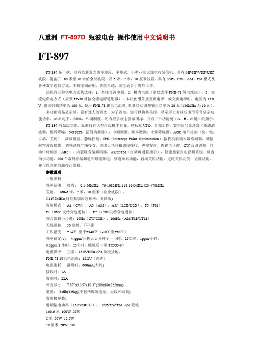
八重洲FT-897D短波电台操作使用中文说明书FT-897FT-897是一款,具有创新观念的多波段,多模式,小型业余无线电收发信机,具有MF/HF/VHF/UHF 波段。
覆盖了160米至10米的全部波段,及6米,2米,70厘米波段。
具有SSB,CW,AM,FM模式及各种数字通信方式。
本机坚固耐用,性能卓越,完全适合于野外工作。
此机有三种供电方式供选择,1,外接直流电源,2,机内电池(需要选件FNB-78氢电池块),3,交流电供电方式(需要FP-30外接交流电源适配器)。
本机使用外接直流电源,或交流电源时,电压为13.8 V,输出射频功率为100瓦。
使用FNB-78镍氢电池时,机器自动调整输出功率为20瓦(430MHz为10瓦)。
多功能液晶显示屏,设有迷人的背光,为了省电,您可以将其关掉。
显示屏上有柱状图形符号显示功能功率,ALC电平,SWR,和调制度。
还有很多状态指示图标。
并有三个功能键(A,B,C键)的指示。
FT-897的高级功能,原来只有大型台式机才具备。
包括双VFO,异频工作,数字信号处理器(带通滤波器,数码降噪,NOTCH,话筒均衡器),中频调整,频率微调,中频降噪器,AGC电平控制(快,慢,自动,关闭),高放增益,静噪控制,IPO(Intercept Point Optimization),接收机前端末级衰减器,调幅航空波段接收,调频调频广播接收,美国天气预报波段接收。
声控发射,内置电子键,CW音调调整,自动中转频差(ARS),内置哑音编解码器,ARTSTM(自动可通联指示),智能搜索自动存频系统。
频谱指示功能。
200个常规存储频道和最爱频道,频道命名功能,自动关机功能,定时关机功能,克隆功能,并可以方便的联接计算机。
参数说明一般参数频率范围:接收:0.1-56MHz,76-108MHz,118-164MHz,420-470MHz发射:160-6米,2米,70厘米(业余波段),5.1675MHz(阿拉斯加应急频率:美国版)发射模式:A1(CW),A3(AM),A3J(LSB/USB),F3(FM)F1(9600波特分包通信),F2(1200波特分包通信)频合器最小步进:10Hz(CW/SSB),100Hz(AM/FM/WFM)天线阻抗:50欧姆,不平衡工作温度:+14℉至于+140℉(-10℃至+60℃)频率稳定度:±4ppm/开机后1分钟至一小时,25℃时。
FAIRCHILD FDS8978 说明书
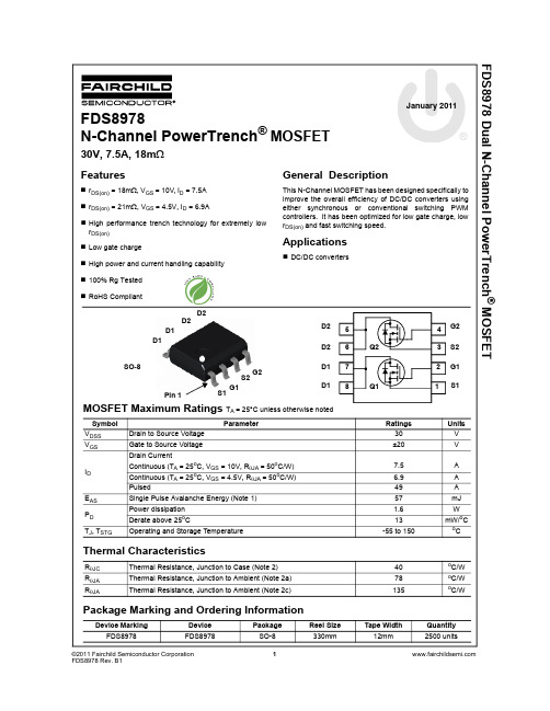
® MOSFETG2S2G1S1D2D2D1D1Pin 1MOSFET Maximum Ratings T A = 25°C unless otherwise noted® MOSFETQ g(TOT)Total Gate Charge at 10V V GS = 0V to 10V V DD= 15VI D = 7.5A-1726nC Q g(5)Total Gate Charge at 5V V GS = 0V to 5V -914nC Q gs Gate to Source Gate Charge - 2.3-nC Q gs2Gate Charge Threshold to Plateau - 1.5-nC Q gdGate to Drain “Miller” Charge- 3.3-nCSwitching Characteristics (V GS = 10V)t ON Turn-On Time V DD = 15V, I D = 7.5A V GS = 10V, R GS = 16Ω-4466ns t d(ON)Turn-On Delay Time -710.5ns t r Rise Time-3755.5ns t d(OFF)Turn-Off Delay Time -4872ns t f Fall Time -2436ns t OFFTurn-Off Time-72108nsDrain-Source Diode CharacteristicsV SD Source to Drain Diode Voltage I SD = 7.5A -- 1.25V I SD = 2.1A-- 1.0V t rr Reverse Recovery Time I SD = 7.5A, dI SD /dt = 100A/µs -1925ns Q RRReverse Recovered ChargeI SD = 7.5A, dI SD /dt = 100A/µs-1013nCNotes:1:Starting T J = 25°C, L = 1mH, I AS = 7.5A, V DD = 30V, V GS = 10V.2:R θJA is the sum of the junction-to-case and case-to-ambient thermal resistance where the case thermal reference is defined as the solder mounting surface of the drain pins. R θJC is guaranteed by design while R θJA is determined by the user’s board design. a) 78°C/W when mounted on a 0.5 in 2 pad of 2 oz copper. b) 125°C/W when mounted on a 0.02 in 2 pad of 2 oz copper. c) 135°C/W when mounted on a minimun pad.MOSFETMOSFETMOSFET® MOSFET3. The use of external heat sinks.4. The use of thermal vias.5. Air flow and board orientation.6. For non steady state applications, the pulse width, the duty cycle and the transient thermal response of the part, the board and the environment they are in.Fairchild provides thermal information to assist the design-er’s preliminary application evaluation. Figure 21 defines the R θJA for the device as a function of the top copper (compo-nent side) area. This is for a horizontally positioned FR-4 board with 1oz copper after 1000 seconds of steady state power with no air flow. This graph provides the necessary in-formation for calculation of the steady state junction temper-ature or power dissipation. Pulse applications can be evaluated using the Fairchild device Spice thermal model or manually utilizing the normalized maximum transientmodels. A listing of the model component values is available in Table 1.1001502000.0010.010.111050Figure 21. Thermal Resistance vs MountingPad AreaR θJA = 64 + 26/(0.23+Area)R θJ A (o C /W )AREA, TOP COPPER AREA (in 2)030609012015010-1100101102103Figure 22. Thermal Impedance vs Mounting Pad Areat, RECTANGULAR PULSE DURATION (s)Z θJ A , T H E R M A L COPPER BOARD AREA - DESCENDING ORDER 0.04 in 20.28 in 20.52 in 20.76 in 21.00 in 2I M P E D A N C E (o C /W )® MOSFETMmed 16 6 8 8 MmedMOD Mstro 16 6 8 8 MstroMODMweak 16 21 8 8 MweakMOD Rbreak 17 18 RbreakMOD 1Rdrain 50 16 RdrainMOD 1.6e-3Rgate 9 20 2.3RSLC1 5 51 RSLCMOD 1e-6RSLC2 5 50 1e3Rsource 8 7 RsourceMOD 8.9e-3Rvthres 22 8 RvthresMOD 1Rvtemp 18 19 RvtempMOD 1S1a 6 12 13 8 S1AMOD S1b 13 12 13 8 S1BMOD S2a 6 15 14 13 S2AMOD S2b 13 15 14 13 S2BMOD Vbat 22 19 DC 1ESLC 51 50 VALUE={(V(5,51)/ABS(V(5,51)))*(PWR(V(5,51)/(1e-6*170),5))}.MODEL DbodyMOD D (IS=2.0E-12 IKF=10 N=1.01 RS=7.0e-3 TRS1=8e-4 TRS2=2e-7+ CJO=3.5e-10 M=0.55 TT=7e-11 XTI=2).MODEL DbreakMOD D (RS=0.2 TRS1=1e-3 TRS2=-8.9e-6).MODEL DplcapMOD D (CJO=3.8e-10 IS=1e-30 N=10 M=0.45).MODEL MstroMOD NMOS (VTO=2.36 KP=150 IS=1e-30 N=10 TOX=1 L=1u W=1u).MODEL MmedMOD NMOS (VTO=1.95 KP=5.0 IS=1e-30 N=10 TOX=1 L=1u W=1u RG=2.3).MODEL MweakMOD NMOS (VTO=1.57 KP=0.02 IS=1e-30 N=10 TOX=1 L=1u W=1u RG=23 RS=0.1).MODEL RbreakMOD RES (TC1=8.3e-4 TC2=-8e-7).MODEL RdrainMOD RES (TC1=15e-3 TC2=0.1e-5).MODEL RSLCMOD RES (TC1=1e-4 TC2=1e-6).MODEL RsourceMOD RES (TC1=1e-3 TC2=3e-6).MODEL RvtempMOD RES (TC1=-1.8e-3 TC2=2e-7).MODEL RvthresMOD RES (TC1=-2.0e-3 TC2=-6e-6)MODEL S1AMOD VSWITCH (RON=1e-5 ROFF=0.1 VON=-4 VOFF=-3.5).MODEL S1BMOD VSWITCH (RON=1e-5 ROFF=0.1 VON=-3.5 VOFF=-4).MODEL S2AMOD VSWITCH (RON=1e-5 ROFF=0.1 VON=-1.5 VOFF=-1.0).MODEL S2BMOD VSWITCH (RON=1e-5 ROFF=0.1 VON=-1.0 VOFF=-1.5).ENDSNote: For further discussion of the PSPICE mod-el, consult A New PSPICE Sub-Circuit for the Power MOSFET Featuring GlobalTemperature Options ; IEEE Power Electronics Specialist Conference Records, 1991, written by William J. Hepp and C. Frank Wheatley.6858+-RVTEMPVBAT RVTHRESIT192213S1BS2BCACB EGSEDS148+-+-® MOSFETspe.evthres n6 n21 n19 n8 = 1spe.evtemp n20 n6 n18 n22 = 1i.it n8 n17 = 1l.lgate n1 n9 = 5.29e-9l.ldrain n2 n5 = 1.0e-9l.lsource n3 n7 = 0.18e-9res.rlgate n1 n9 = 52.9res.rldrain n2 n5 = 10res.rlsource n3 n7 = 1.8m.mmed n16 n6 n8 n8 = model=mmedmod, l=1u, w=1u m.mstrong n16 n6 n8 n8 = model=mstrongmod, l=1u, w=1u m.mweak n16 n21 n8 n8 = model=mweakmod, l=1u, w=1u res.rbreak n17 n18 = 1, tc1=8.3e-4,tc2=-8e-7res.rdrain n50 n16 = 1.6e-3, tc1=15e-3,tc2=0.1e-5res.rgate n9 n20 = 2.3res.rslc1 n5 n51 = 1e-6, tc1=1e-4,tc2=1e-6res.rslc2 n5 n50 = 1e3res.rsource n8 n7 = 8.9e-3, tc1=1e-3,tc2=3e-6res.rvthres n22 n8 = 1, tc1=-2.0e-3,tc2=-6e-6res.rvtemp n18 n19 = 1, tc1=-1.8e-3,tc2=2e-7sw_vcsp.s1a n6 n12 n13 n8 = model=s1amod sw_vcsp.s1b n13 n12 n13 n8 = model=s1bmod sw_vcsp.s2a n6 n15 n14 n13 = model=s2amod sw_vcsp.s2b n13 n15 n14 n13 = model=s2bmodv.vbat n22 n19 = dc=1equations {i (n51->n50) +=iscliscl: v(n51,n50) = ((v(n5,n51)/(1e-9+abs(v(n5,n51))))*((abs(v(n5,n51)*1e6/170))** 5))}}68+-58+-RBREAKRVTEMPVBAT RVTHRESIT17181922121315S1AS1BS2A S2BCACB EGSEDS1481381413RSOURCESOURCE73RLSOURCE 8+--® MOSFETctherm.ctherm1 th 8 =2.0e-3ctherm.ctherm2 8 7 =5.0e-3ctherm.ctherm3 7 6 =1.0e-2ctherm.ctherm4 6 5 =4.0e-2ctherm.ctherm5 5 4 =9.0e-2ctherm.ctherm6 4 3 =2e-1ctherm.ctherm7 3 2 1ctherm.ctherm8 2 tl 3rtherm.rtherm1 th 8 =1e-1rtherm.rtherm2 8 7 =5e-1rtherm.rtherm3 7 6 =1rtherm.rtherm4 6 5 =5rtherm.rtherm5 5 4 =8rtherm.rtherm6 4 3 =12rtherm.rtherm7 3 2 =18rtherm.rtherm8 2 tl =25}TABLE 1. THERMAL MODELSCOMPONANT 0.04 in 20.28 in 20.52 in 20.76 in 2 1.0 in 2CTHERM6 1.2e-1 1.5e-1 2.0e-1 2.0e-1 2.0e-1CTHERM70.5 1.0 1.0 1.0 1.0CTHERM8 1.3 2.8 3.0 3.0 3.0RTHERM62620151312RTHERM73924211918RTHERM85538.731.329.725RTHERM6RTHERM8RTHERM7RTHERM5CTHERM6CTHERM5tl 234CASECTHERM7CTHERM8*Trademarks of System General Corporation, used under license by Fairchild Semiconductor.DISCLAIMER FAIRCHILD SEMICONDUCTOR RESERVES THE RIGHT TO MAKE CHANGES WITHOUT FURTHER NOTICE TO ANY PRODUCTS HEREIN TO IMPROVE RELIABILITY, FUNCTION, OR DESIGN. FAIRCHILD DOES NOT ASSUME ANY LIABILITY ARISING OUT OF THE APPLICATION OR USE OF ANY PRODUCT OR CIRCUIT DESCRIBED HEREIN; NEITHER DOES IT CONVEY ANY LICENSE UNDER ITS PATENT RIGHTS, NOR THE RIGHTS OF OTHERS.THESE SPECIFICATIONS DO NOT EXPAND THE TERMS OF FAIRCHILD’S WORLDWIDE TERMS AND CONDITIONS, SPECIFICALLY THE WARRANTY THEREIN, WHICH COVERS THESE PRODUCTS.LIFE SUPPORT POLICY FAIRCHILD’S PRODUCTS ARE NOT AUTHORIZED FOR USE AS CRITICAL COMPONENTS IN LIFE SUPPORT DEVICES OR SYSTEMS WITHOUT THE EXPRESS WRITTEN APPROVAL OF FAIRCHILD SEMICONDUCTOR CORPORATION.As used here in:1. Life support devices or systems are devices or systems which, (a) areintended for surgical implant into the body or (b) support or sustain life,and (c) whose failure to perform when properly used in accordance withinstructions for use provided in the labeling, can be reasonablyexpected to result in a significant injury of the user. 2. A critical component in any component of a life support, device, or system whose failure to perform can be reasonably expected to cause the failure of the life support device or system, or to affect its safety or effectiveness.PRODUCT STATUS DEFINITIONS Definition of TermsAccuPower™Auto-SPM™Build it Now™CorePLUS™CorePOWER™CROSSVOLT ™CTL™Current Transfer Logic™DEUXPEED ®Dual Cool™EcoSPARK ®EfficentMax™ESBC™Fairchild ®Fairchild Semiconductor ®FACT Quiet Series™FACT ®FAST ®FastvCore™FETBench™FlashWriter ® *FPS™F-PFS™FRFET®Global Power Resource SM Green FPS™Green FPS™ e-Series™G max ™GTO™IntelliMAX™ISOPLANAR™MegaBuck™MICROCOUPLER™MicroFET™MicroPak™MicroPak2™MillerDrive™MotionMax™Motion-SPM™OptiHiT™OPTOLOGIC ®OPTOPLANAR ®®PDP SPM™Power-SPM™PowerTrench PowerXS™Programmable Active Droop™QFET ®QS™Quiet Series™RapidConfigure™ Saving our world, 1mW/W/kW at a time™SignalWise™SmartMax™SMART START™SPM ®STEALTH™SuperFET ®SuperSOT™-3SuperSOT™-6SuperSOT™-8SupreMOS ®SyncFET™Sync-Lock™ ®*The Power Franchise The Right Technology for Your Success™®TinyBoost™TinyBuck™TinyCalc™TinyLogic ®TINYOPTO™TinyPower™TinyPWM™TinyWire™TriFault Detect™TRUECURRENT™*μSerDes™UHC ®Ultra FRFET™UniFET™VCX™VisualMax™XS™®Datasheet IdentificationProduct Status Definition Advance InformationFormative / In Design Datasheet contains the design specifications for product development. Specifications may change in any manner without notice.ANTI-COUNTERFEITING POLICY Fairchild Semiconductor Corporation’s Anti-Counterfeiting Policy. Fairchild’s Anti-Counterfeiting Policy is also stated on our external website,, under Sales Support .Counterfeiting of semiconductor parts is a growing problem in the industry. All manufactures of semiconductor products are experiencing counterfeiting of their parts. Customers who inadvertently purchase counterfeit parts experience many problems such as loss of brand reputation, substandard performance, failed application, and increased cost of production and manufacturing delays. Fairchild is taking strong measures to protect ourselves and our customers from the proliferation of counterfeit parts. Fairchild strongly encourages customers to purchase Fairchild parts either directly from Fairchild or from Authorized Fairchild Distributors who are listed by country on our web page cited above. Products customers buy either from Fairchild directly or from Authorized Fairchild Distributors are genuine parts, have full traceability, meet Fairchild’s quality standards for handing and storage and provide access to Fairchild’s full range of up-to-date technical and product information. Fairchild and our Authorized Distributors will stand behind all warranties and will appropriately address and warranty issues that may arise. Fairchild will not provide any warranty coverage or other assistance for parts bought from Unauthorized Sources. Fairchild is committed to combat this global problem and encourage our customers to do their part in stopping this practice by buying direct or from authorized distributors.™©2011 Fairchild Semiconductor CorporationFDS8978 Rev. 11。
897说明书

前面板控制钮及开关1 液晶显示屏液晶显示屏(lcd)用来显示工作频率及电台的其它工作状况 2 func(功能)键这三个键用来选择很多最重要的电台操作特性。
按一下[f]键,然后旋转mem/v of ch旋钮,相应的功能键就[a)[b][c]三个键的上方(在lcd的底部),通过这三个键可以选择17组功能。
3 mic插座将配套的mh-31手持话筒插在这个插座中4 phone插口这个1/4英寸,3接点的插座用来连接单声道或立体声的耳机。
耳机插入后,主机扬声器就静音了。
耳机音量用af钮来调整。
5 电源开关按住这个开关1秒钟,就可以开启或关闭电台电源。
电源开启时,轻按一下这个键,就可以调整频率调谐的速度,在快速调谐状态下,屏幕右下角会出现一个跑步者的图形6 [f]键按一下这个键后可以通过旋转mem/vfo ch旋钮来改变多功能键([a],[b][c])的功能按住这个键一秒钟则可以激活相应的菜单模式。
7 lock键按一下这个键可以锁住前面板上的功能按键/旋钮,以防止无意间改变工作频率。
8 主旋钮dial这是电台的主要调谐旋钮。
可以用来调节频率以及“菜单”中的各项设置。
9 af旋钮这个旋钮是复合钮的内圈,用来调节内置扬声器或外接喇叭的音量。
顺时针为加大音量10 sql/rf旋钮这个旋钮是复合旋钮的外围,用来调节接收时射频及中频的电平,也可以通过菜单模式no-08c [sql/rf gain)的设置,用来调节静噪水平。
出厂时的缺省设置就是静噪调节状态。
11 clar/if shift键按动这个键可以激活接收信号时的清音功能。
这个功能是用来调节最大±9.99khz的频偏。
发射频率不受这个调节的影响。
按住这个键一秒钟就激活了if(中频)频偏功能,用来调节中频滤波器的频带中心频率。
12 clar旋钮当按一下clar/if shift钮以后,旋转clar旋钮就可以在±9.99khz的范围内调节清音器13 band(dwn)/band(up)按键这两个键是用来向上(up)或向下(dwn)移动频带的,可以选择的频带顺序如下:14 mem/vfo ch旋钮这个旋钮可以用来调节工作频率、存储信道以及[a],[b],[c]功能选择。
Mellanox InfiniBand路由器SB7780和SB7880的产品介绍说明书

©2020 Mellanox Technologies. All rights reserved.†For illustration only. Actual products may vary.SB7780 and SB7880 InfiniBand routers enable new levels of subnets isolation and compute-to-storage connectivity, critical to large-scale and diverse data-centers.Scaling-Out Data Centers with EDR 100G InfiniBandHigh Performance Computing (HPC), Artificial Intelligence (AI), and Data-Intensive and Cloud infrastructures all leverage InfiniBand’s high data throughput, extremely low latency, and smart In-Network Computing acceleration engines to deliver world-leading application performance and scalability, while reducing operational costs and infrastructure complexity. Mellanox’s innovative In-Networking-based Scalable Hierarchical Aggregation and Reduction Protocol (SHARP)™ technology enables the acceleration of communications frameworks using embedded hardware, resulting in order of magnitude application and performance improvements.In cases where the separation between InfiniBand subnets and keeping connectivity to a central InfiniBand Storage are required, InfiniBand Routers are the ideal solution.Sustained Network PerformanceSB7780 / SB7880 InfiniBand routers are based on Switch-IB ® / Switch-IB ® 2 ASICs, respectively. They offer fully-flexible 36 EDR 100Gb/s ports that can be split among several different subnets. InfinBand routers bring two major enhancements to the Mellanox InfiniBand portfolio:•Increase resiliency by s plitting the data center’s network into several subnets; each subnet runs itsown subnet manager, effectively isolating each subnet from the others’ availability or instability •Enable multiple compute to storage connections while separately isolating login access to each compute subnetWorld-Class DesignSB7780 / SB7880 InfiniBand routers are elegantly designed for performance, serviceability, energy savings and high-availability. They come equipped with two highly efficient, 80 gold+ and energy star certified, power supplies.Their best-in-class design enables the EDR IB routers to support low power consumption, with ATIS weighted power consumption as low as 122W for a fully populated system. This means more power reduction if not all ports are used or fully utilized.SB7780 / SB7880 also have redundant power supplies (1+1) and their fans draw (N+1) both with air shutters for achieving maximal thermal protection.36-port Non-blocking Managed EDR 100Gb/s InfiniBand RoutersInfiniBand EDR 100Gb/s RoutersPRODUCT BRIEFSWITCH SYSTEM †© Copyright 2020. Mellanox Technologies. All rights reserved. Mellanox, Mellanox logo, MLNX-OS , Switch-IB, and UFM are registered trademarks of Mellanox Technologies, Ltd. Switch-IB, UFM and Unified Fabric Manager are trademarks of Mellanox Technologies, Ltd. All other trademarks are property of their respective owners.350 Oakmead Parkway, Suite 100, Sunnyvale, CA 94085Tel: 408-970-3400 • Fax: Mellanox SB7700 and SB7880 InfiniBand Routerspage 2ManagementThe InfiniBand router’s dual-core x86 CPU runs MLNX-OS ® software package, which delivers complete chassis management of the router’s firmware, power supplies, fans and ports. The router can also becoupled with Mellanox’s Unified Fabric Manager (UFM ®) platforms to manage scale-out InfiniBand computing environments.Revolutionizing data center management, the UFM family of products combine enhanced, real-time network telemetry with AI-poweredcyber intelligence and analytics. The UFM solutions minimize downtime by enabling system admins to quickly detect and respond to potential security threats and operational issues, and predict upcoming failures.Mellanox SB7780 / SB7880–19’’ rack mountable 1U chassis –36 QSFP28 non-blocking ports with aggregate data throughput up to 7Tb/s (EDR)Router Specifications–Compliant with IBTA 1.21 and 1.3 –9 virtual lanes: 8 data + 1 management–256 to 4Kbyte MTU–8X 48K entry linear forwarding databaseManagement Ports–100/1000Mb/s Ethernet ports –RS232 port over DB9–USB port –DHCP–Familiar Industry Standard CLI –Management over IPv6 –Management IP –SNMP v1,v2,v3 –Web UIFabric Management–Unified Fabric Manager (UFM™) AgentConnectors and Cabling–QSFP28 connectors–Passive copper or active fiber cables –Optical modulesIndicators–Per port status LED Link, Activity –System status LEDs: System, fans, power supplies –Port Error LED –Unit ID LEDPhysical Characteristics–Dimensions: 1.7’’ (43.6 mm) H x 16.85’’ (428mm) W x 27’’ (685.8mm) D –Weight: 11kg (24.2lb)Power Supply–Dual redundant slots –Hot plug operation –Input range:100-127 VAC, 200-240VAC–Frequency: 50-60Hz, single phase AC, 4.5A, 2.9ACooling–Front-to-rear or rear-to-front cooling option–Hot-swappable fan unitPower Consumption–Typical Power with Passive Cables (ATIS): 136WFEATURESSafety–CB –cTUVus –CE –CUEMC (Emissions)–CE –FCC–VCCI –ICES –RCMOperating Conditions–Temperature:–Operating 0ºC to 45ºC–Non-operating -40ºC to 70ºC–Humidity:–Operating 10% to 85% non-condensing–Non-operating 10% to 90% non-condensing–Altitude: Operating -60m to 3200mAcoustic–ISO 7779 –ETS 300 753Others–RoHS compliant –Rack-mountable, 1U –1-year warrantyCOMPLIANCETable 1 - Part Numbers and Descriptions*P 2C is connector side outlet; C 2P is connector side inlet.15-7858PB Rev 1.3。
mt8979中文资料_数据手册_IC数据表
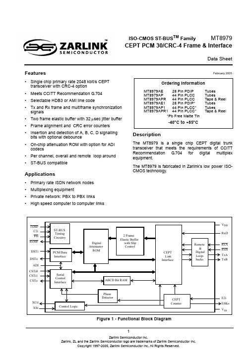
1Features•Single chip primary rate 2048 kbit/s CEPT transceiver with CRC-4 option •Meets CCITT Recommendation G.704•Selectable HDB3 or AMI line code•Tx and Rx frame and multiframe synchronization signals•Two frame elastic buffer with 32µsec jitter buffer •Frame alignment and CRC error counters •Insertion and detection of A, B, C, D signalling bits with optional debounce•On-chip attenuation ROM with option for ADI codecs•Per channel, overall and remote loop around •ST-BUS compatibleApplications•Primary rate ISDN network nodes •Multiplexing equipment•Private network: PBX to PBX links •High speed computer to computer linksDescriptionThe MT8979 is a single chip CEPT digital trunk transceiver that meets the requirements of CCITT Recommendation G.704 for digital multiplex equipment.The MT8979 is fabricated in Zarlink’s low power ISO-CMOS technology.February 2005Ordering InformationMT8979AE 28 Pin PDIP Tubes MT8979AP 44 Pin PLCC TubesMT8979APR 44 Pin PLCC Tape & Reel MT8979AE128 Pin PDIP*Tubes MT8979AP144 Pin PLCC*TubesMT8979APR144 Pin PLCC*Tape & Reel*Pb Free Matte Tin-40°C to +85°CISO-CMOS ST-BUS TM FamilyMT8979CEPT PCM 30/CRC-4 Frame & InterfaceData SheetFigure 1 - Functional Block DiagramV DDRxDRxA RxB TxA TxBE2i E8Ko V SSCEPT Link InterfaceDigital Attenuator ROMST-BUS Timing CircuitryPCM/Data InterfaceSerial Control InterfaceABCD Bit RAMControl LogicPhase DetectorCEPT CounterTxMF C2i F0i RxMF DSTi DSTo ADI CSTi0CSTi1CSToXCtl XStRemote &Digital Loop-backs2 Frame Elastic Buffer with Slip ControlMT8979Data SheetFigure 2 - Pin ConnectionsPin Description Pin #Name DescriptionDIPPLCC12TxA Transmit A (Output): A split phase unipolar signal suitable for use with TxB and an external line driver and transformer to construct the bipolar line signal.23TxB Transmit B (Output :) A split phase unipolar signal suitable for use with TxA and an external line driver and transformer to construct the bipolar line signal.35DSTo Data ST-BUS (Output): A 2048kbit/s serial output stream which contains the 30 PCM or data channels received from the CEPT line.44NC No Connection.59RxA Receive A (Input): Received split phase unipolar signal decoded from a bipolar line receiver.610RxB Receive B (Input): Received split phase unipolar signal decoded from a bipolar line receiver.711RxD Received Data (Input): Input of the unipolar data generated from the line receiver. This data may be NRZ or RZ.813CSTi1Control ST-BUS Input #1: A 2048kbit/s stream that contains channel associated signalling, frame alignment and diagnostic functions.9NC No Connection.10NCNo Connection.44 PIN PLCC1234567891011121314151617181920282726252423222128 PIN PDIPTxA TxB NC RxA RxB RxD CSTi1NC NC ADI CSTi0E8Ko VSSVDD IC F0i E2i NC RxMF TxMF C2i NC DSTi NC CSTo XSt XCtlDSTo V S S D S T o T x B T x A I C N C F 0i N C E 2iNC RxMF TxMF NC NC C2i NC NC NC NC NCNC NC RxA RxB RxD NC CSTi1NC NC NC ADIV S S C S T i 0E 8K o N C V S S X S t N C C S T o N C D S T iX C t l V D D 1654324443424140789101112131415163938373635343332313023181920212224252627281729N CMT8979Data Sheet1117ADIAlternate Digit Inversion (Input): If this input is high, the CEPT timeslots which arespecified on CSTi0 as voice channels are ADI coded and decoded. When this bit is low it disables ADI coding for all channels. This feature allows either ADI or non-ADI codecs to be used on DSTi and DSTo.1219CSTi0Control ST-BUS Input #0: A 2048kbit/s stream that contains 30 per channel control words and two Master Control Words.1320E8KoExtracted 8kHz Clock (Output): An 8kHz output generated by dividing the extracted 2048kHz clock by 256 and aligning it with the received CEPT frame. The 8kHz signal can be used for synchronizing the system clock to the extracted 2048kHz clock. Only valid when device achieves synchronization (goes low during a loss of signal or a loss of basic frame synchronization condition).E8Ko goes high impedance when 8kHzSEL = 0 in MCW2.1523XCtlExternal Control (Output): An uncommitted external output pin which is set or reset via bit 1 in Master Control Word 2 on CSTi0. The state of XCtl is updated once per frame.1624XSt External Status : The state of this pin is sampled once per frame and the status is reported in bit 1 of the Master Status Word 1 on CSTo.1726CSTo Control ST-BUS Output : A 2048kbit/s serial control stream which provides the 16signalling words, two Master Status Words, Phase Status Word and CRC Error Count.18NCNo Connection.1928DSTi Data ST-BUS Input : This pin accepts a 2048kbit/s serial stream which contains the 30PCM or data channels to be transmitted on the CEPT trunk.20NCNo Connection.2134C2i2048kbit/s System Clock (Input): The master clock for the ST-BUS section of the chip. All data on the ST-BUS is clocked in on the falling edge of the C2i and output on the rising edge. The falling edge of C2i is also used to clock out data on the CEPT transmit link.2237TxMFTransmit Multiframe Boundary (Input): This input can be used to set the channel associated and CRC transmitted multiframe boundary (clear the frame counters). The device will generate its own multiframe if this pin is held high.2338RxMFReceived Multiframe Boundary (Output): An output pulse delimiting the received Multiframe boundary. (This multiframe is not related to the received CRC multiframe.)The next frame output on the data stream (DSTo) is received as frame 0 on the CEPT link.24NC No Connection.2540E2iExtracted 2048kHz Clock (Input): The falling edge of this 2048kHz clock is used to latch the received data (RxD). This clock input must be derived from the CEPT received data and must have its falling edge aligned with the center of the received bit (RxD).Pin Description (continued)Pin #Name DescriptionDIPPLCCMT8979Data SheetFunctional DescriptionThe MT8979 is a CEPT trunk digital link interface conforming to CCITT Recommendation G.704 for PCM 30 and I.431 for ISDN. It includes features such as: insertion and detection of synchronization patterns, optional cyclical redundancy check and far end error performance reporting, HDB3 decoding and optional coding, channel associated or common channel signalling, programmable digital attenuation and a two frame received elastic buffer. The MT8979 can also monitor several conditions on the CEPT digital trunk, which include, frame and multiframe synchronization, received all 1’s alarms, data slips as well as framing and CRC errors, both near and far end.The system interface to the MT8979 is a TDM bus structure that operates at 2048kbit/s known as the ST-BUS.This serial stream is divided into 125µs frames that are made up of 32 x 8 bit channels.The line interface to the MT8979 consists of split phase unipolar inputs and outputs which are supplied from/to a bipolar line receiver/driver, respectively.Figure 3 - CEPT Link Frame & Multiframe FormatCEPT InterfaceThe CEPT frame format consists of 32, 8 bit timeslots. Of the 32 timeslots in a frame, 30 are defined as information channels, timeslots 1-15 and 17-31 which correspond to telephone channels 1-30. An additional voice/data channel may be obtained by placing the device in common channel signalling mode. This allows use of timeslot 16 for 64kbit/s common channel signalling.2642F0i Frame Pulse Input : The ST-BUS frame synchronization signal which defines the beginning of the 32 channel frame.2744IC Internal Connection : Tie to V SS (Ground) for normal operation. 281V DD Positive Power Supply Input (+5 Volts).146,8,22V SSNegative Power Supply Input (Ground).Pin Description (continued)Pin #Name DescriptionDIPPLCCFrame 1514150Timeslot13031Most Significant Bit (First)LeastSignificant Bit (Last)Bit 12345678Frame Frame Frame Frame TimeslotTimeslotTimeslotBit Bit Bit Bit Bit Bit Bit 2.0 ms(8/2.048) µs125 µs ••••••••••••MT8979Data SheetSynchronization is included within the CEPT bit stream in the form of a bit pattern inserted into timeslot 0. The contents of timeslot 0 alternate between the frame alignment pattern and the non-frame alignment pattern as described in Figure 4. Bit 1 of the frame alignment and non-frame alignment bytes have provisions for additional protection against false synchronization or enhanced error monitoring. This is described in more detail in the following section.In order to accomplish multiframe synchronization, a 16 frame multiframe is defined by sending four zeros in the high order quartet of timeslot 16 frame 0, i.e., once every 16 frames (see Figure 5). The CEPT format has four signalling bits, A, B, C and D. Signalling bits for all 30 information channels are transmitted in timeslot 16 of frames 1 to 15. These timeslots are subdivided into two quartets (see Table 6).Figure 4 - Allocation of Bits in Timeslot 0 of the CEPT LinkNote 1 : With CRC active, this bit is ignored.Note 2 : With SiMUX active, this bit transmits SMF CRC results in frames 13 and 15Note 3 : Reserved for National use.Figure 5 - Allocation of Bits in Timeslot 16 of the CEPT LinkCyclic Redundancy Check (CRC)An optional cyclic redundancy check (CRC) has been incorporated within CEPT bit stream to provide additional protection against simulation of the frame alignment signal, and/or where there is a need for an enhanced error monitoring capability. The CRC process treats the binary string of ones and zeros contained in a submultiframe (with CRC bits set to binary zero) as a single long binary number. This string of data is first multiplied by x 4 then divided by the generating polynomial x 4+x+1. This division process takes place at both the transmitter and receiver end of the link. The remainder calculated at the receiver is compared to the one received with the data over the link. If they are the same, it is of high probability that the previous submultiframe was received error free.The CRC procedure is based on a 16 frame multiframe, which is divided into two 8 frame submultiframes (SMF).The frames which contain the frame alignment pattern contain the CRC bits, C 1 to C 4 respectively, in the bit 1position. The frames which contain the non-frame alignment pattern contain within the bit 1 position, a 6 bit CRC multiframe alignment signal and two spare bits (in frames 13 and 15), which are used for CRC error performance reporting (refer to Figure 6). During the CRC encoding procedure the CRC bit positions are initially set at zero. The remainder of the calculation is stored and inserted into the respective CRC bits of the next SMF. The decoding process repeats the multiplication division process and compares the remainder with the CRC bits received in the next SMF.Bit Number12345678Timeslot 0 containing the frame alignment signal Reserved for International use (1)1111Timeslot 0 containing the non-frame alignment signalReserved for International use (2)1Alarm indication to the remote PCM multiplex equipment See Note #3See Note #3See Note #3See Note #3See Note #3Timeslot 16 of frame 0Timeslot 16 of frame 1• • •Timeslot 16 of frame 150000XYXXABCD bits for telephone channel 1 (timeslot 1)ABCD bits for telephone channel 16 (timeslot 17)ABCD bits for telephone channel 15 (timeslot 15)ABCD bits for telephone channel 30 (timeslot 31)MT8979Data SheetThe two spare bits (denoted Si1 and Si2 in Figure 6) in the CRC-4 multiframe are used to monitor far-end error performance. The results of the CRC-4 comparisons for the previously received SMFII and SMFI are encoded and transmitted back to the far end in the Si bits (refer to Table 1).Table 1 - Coding of Spare Bits Si1 and Si2Figure 6 - CRC Bit Allocation and SubmultiframingNote 1 : Remote Alarm. Keep at 0 for normal operation.Note 2 : Reserved for National use. Keep at 1 for normal operation.Note 3 : Used to monitor far-end CRC error performance.Si1 bit (frame 13)Si2 bit (frame 15)Meaning11CRC results for both SMFI, II are error free.10CRC result for SMFII is in error.CRC result for SMFI is error free.01CRC result for SMFII is error free.CRC result for SMFI is in error.0CRC results for both SMFI, II are in error.Multiple Frame ComponentFrame TypeCRC Frame #Timeslot Zero12345678Frame Alignment Signal 0C 10011011Non-Frame Alignment Signal101A (1)Sn (2)Sn (2)Sn (2)Sn (2)Sn (2)S Frame Alignment Signal 2C 20011011M Non-Frame Alignment Signal 301A (1)Sn (2)Sn (2)Sn (2)Sn (2)Sn (2)F Frame Alignment Signal 4C 30011011Non-Frame Alignment Signal 511A (1)Sn (2)Sn (2)Sn (2)Sn (2)Sn (2)IFrame Alignment Signal 6C 40011011Non-Frame Alignment Signal 701A (1)Sn (2)Sn (2)Sn (2)Sn (2)Sn (2)Frame Alignment Signal8C 10011011S Non-Frame Alignment Signal 911A (1)Sn (2)Sn (2)Sn (2)Sn (2)Sn (2)M Frame Alignment Signal 10C 20011011F Non-Frame Alignment Signal 1111A (1)Sn (2)Sn (2)Sn (2)Sn (2)Sn (2)Frame Alignment Signal 12C 30011011I Non-Frame Alignment Signal 13Si1(3)1A (1)Sn (2)Sn (2)Sn (2)Sn (2)Sn (2)IFrame Alignment Signal 14C 40011011Non-Frame Alignment Signal15Si2(3)1A (1)Sn (2)Sn (2)Sn (2)Sn (2)Sn (2)MT8979Data SheetFigure 7 - ST-BUS Stream FormatST-BUS InterfaceThe ST-BUS is a synchronous time division multiplexed serial bus with data streams operating at 2048kbit/s and configured as 32, 64kbit/s channels (refer Figure 7). Synchronization of the data transfer is provided from a frame pulse, which identifies the frame boundaries and repeats at an 8kHz rate. Figure 17 shows how the frame pulse (F0i) defines the ST-BUS frame boundaries. All data is clocked into the device on the falling edge of the 2048kbit/s clock (C2i), while data is clocked out on the rising edge of the 2048kbit/s clock at the start of the bit cell.Data Input (DSTi)The MT8979 receives information channels on the DSTi pin. Of the 32 available channels on this serial input, 30are defined as information channels. They are channels 1-15 and 17-31. These 30 timeslots are the 30 telephone channels of the CEPT format numbered 1-15 and 16-30. Timeslot 0 and 16 are unused to allow the synchronization and signalling information to be inserted, from the Control Streams (CSTi0 and CSTi1). The relationship between the input and output ST-BUS stream and the CEPT line is illustrated in Figures 8 to 12. In common channel signalling mode timeslot 16 becomes an active channel. In this mode channel 16 on DSTi is transmitted on timeslot 16 of the CEPT link unaltered. This mode is activated by bit 5 of channel 31 of CSTi0.Control Input 0 (CSTi0)All the necessary control and signalling information is input through the two control streams. Control ST-BUS input number 0 (CSTi0) contains the control information that is associated with each information channel. Each control channel contains the per channel digital attenuation information, the individual loopback control bit, and the voice or data channel identifier, see Table 2. When a channel is in data mode (B7 is high) the digital attenuation and Alternate Digit Inversion are disabled. It should be noted that the control word for a given information channel is input one timeslot early, i.e., channel 0 of CSTi0 controls channel 1 of DSTi. Channels 15 and 31 of CSTi0contain Master Control Words 1 and 2, which are used to set up the interface feature as seen by the respective bit functions of Tables 3 and 4.Control Input 1 (CSTi1)Control ST-BUS input stream number 1 (CSTi1) contains the synchronization information and the A, B, C & D signalling bits for insertion into timeslot 16 of the CEPT stream (refer to Tables 5 to 8). Timeslot 0 contains the four zeros of the multiframe alignment signal plus the XYXX bits (see Figure 5). Channels 1 to 15 of CSTi1 contain the A, B, C & D signalling bits as defined by the CEPT format (see Figure 5), i.e., channel 1 of CSTi1 contains the A,B,C & D bits for DSTi timeslots 1 and 17. Channel 16 contains the frame alignment signal, and channel 17contains the non-frame alignment signal (see Figure 4). Channel 18 contains the Master Control Word 3 (see Table 9). Figure 11 shows the relationship between the control stream (CSTi1) and the CEPT stream.CHANNEL3130BIT CHANNELCHANNELCHANNELCHANNEL310BIT BIT BIT BIT BIT BIT BIT • • •LeastSignificant Bit (Last)Most Significant Bit (First)(8/2.048)µs125µs7654321MT8979Data SheetControl Output (CSTo)Control ST-BUS output (CSTo) contains the multiframe signal from timeslot 16 of frame 0 (see Table 10). Signalling bits A, B, C & D for each CEPT channel are sourced from timeslot 16 of frames 1-15 and are output in channels 1-15 on CSTo , as shown in Table 11. The frame alignment signal and nonframe alignment signal, received from timeslot 0 of alternate frames, are output in timeslots 16 and 17 as shown in Tables 12 and 13.Channel 18 contains a Master Status Word, which provides to the user information needed to determine the operating condition of the CEPT interface i.e., frame synchronization, multiframe synchronization, frame alignment byte errors, slips, alarms, and the logic of the external status pin (see Table 14). Figure 12, shows the relationship between the control stream channels and the CEPT signalling channels in the multiframe. The ERR bit in the Master Status word is an indicator of the number of errored frame alignment bytes that have been received in alternate timeslot zero. The time interval between toggles of the ERR bit can be used to evaluate the bit error rate of the line according to the CCITT Recommendation G.732 (see section on Frame Alignment Error Counter). Channel 19 contains the Phase Status Word (see Table 15), which can be used to determine the phase relationship between the ST-BUS frame pulse (F0i) and the rising edge of E8Ko. This information could be used to determine the long term trend of the received data rate, or to identify the direction of a slip.Channel 20 contains the CRC error count (see Table 16). This counter will wrap around once terminal count is achieved (256 errors). If the maintenance option is selected (bit 3 of MCW3) the counter is reset once per second. Channel 21 contains the Master Status Word 2 (see Table 17). This byte identifies the status of the CRC reframe and CRC sync. It also reports the Si bits received in timeslot 0 of frames 13 and 15 and the ninth and most significant bit (b8) of the 9-bit Phase Status Word.Elastic BufferThe MT8979 has a two frame elastic buffer at the receiver, which absorbs the jitter and wander in the received signal. The received data is written into the elastic buffer with the extracted E2i (2048kHz) clock and read out of the buffer on the ST-BUS side with the system C2i (2048kHz) clock (e.g., PBX system clock). Under normal operating conditions, in a synchronous network, the system C2i clock is phase-locked to the extracted E2i clock. In this situation every write operation to the elastic buffer is followed by a read operation. Therefore, underflow or overflow of data in the elastic buffer will not occur.If the system clock is not phase-locked to the extracted clock (e.g., lower quality link which is not selected as the clock source for the PBX) then the data rate at which the data is being written into the device on the line side may differ from the rate at which it is being read out on the ST-BUS side.When the clocks are not phase-locked, two situations can occur:Case #1: If the data on the line side is being written in at a rate SLOWER than it is being read out on the ST-BUS side, the distance between the write pointer and the read pointer will begin to decrease over time. When the distance is less than two channels, the buffer will perform a controlled slip which will move the read pointers to a new location 34 channels away from the write pointer. This will result in the REPETITION of the received frame. Case #2: If the data on the line side is being written in at a rate FASTER than it is being read out on the ST-BUS side, the distance between the write pointer and the read pointer will begin to increase over time. When the distance exceeds 42 channels, the elastic buffer will perform a controlled slip which will move the read pointer to a new location ten channels away from the write pointer. This will result in the LOSS of the last received frame. Note that when the device performs a controlled slip, the ST-BUS address pointer is repositioned so that there is either a 10 channel or 34 channel delay between the input CEPT frame and the output ST-BUS frame. Since the buffer performs a controlled slip only if the delay exceeds 42 channels or is less than two channels, there is a minimum eight channel hysteresis built into the slip mechanism. The device can, therefore, absorb eight channels or 32.5µs of jitter in the received signal.MT8979Data SheetThere is no loss of frame synchronization, multiframe synchronization or any errors in the signalling bits when the device performs a slip.Figure 8 - Relationship between Input DSTi Channels and Transmitted CEPT TimeslotsFigure 9 - Relationship between Received CEPT Timeslots and Output DSTo ChannelsFigure 10 - Relationship between Input CSTi0 Channels and Controlled CEPT TimeslotsFigure 11 - Relationship between Input CSTi1 Channels and Transmitted CEPT FramesFigure 12 - Relationship between Received CEPT Frames and Output CSTo Channels- *Denotes Unused Channel (CSTo output is not put in high impedance state)-CCS Denotes Signalling Channel if Common Channel Signalling Mode Selected- A Denotes Frame-Alignment Frame-S1 Denotes Master Status Word 1 (MSW1)- N Denotes Non Frame-Alignment Frame-S2 Denotes Phase Status Word (PSW)- C1, C2, C3 Denotes Master Control Words 1,2,3-S3 Denotes CRC Error Count- SIG Denotes Signalling Channel-S4 Denotes Master Status Word 2 (MSW2)DSTiChannel #012345678910111213141516171819202122232425262728293031CEPT Timeslot #123456789101112131415CCS 171819202122232425262728293031DSTi Channel #012345678910111213141516171819202122232425262728293031CEPT Timeslot #123456789101112131415SIG171819202122232425262728293031CSTi0Channel #012345678910111213141516171819202122232425262728293031Device Control C1C2CEPT Channel #Control Word123456789101112131415171819202122232425262728293031CSTi1Channel #012345678910111213141516171819202122232425262728293031DeviceControl C3*************CEPT FRAME #CHANNEL #016116216316416516616716816916101611161216131614161516A 0N 0CSTo Channel #012345678910111213141516171819202122232425262728293031Device StatusS1S2S3S4**********CEPT FRAME #TIMESLOT #016116216316416516616716816916101611161216131614161516A 0N 0MT8979Data SheetFrame Alignment Error CounterThe MT8979 provides an indication of the bit error rate found on the link as required by CCITT Recommendation G.703. The ERR bit (Bit 5 of MSW1) is used to count the number of errors found in the frame alignment signal and this can be used to estimate the bit error rate. The ERR bit changes state when 16 errors have been detected in the frame alignment signal. This bit can not change state more than once every 128 ms, placing an upper limit on the detectable error rate at approximately 10-3. The following formula can be used to calculate the BER:where:7 -is the number of bits in the frame alignment signal (0011011).16 -is the number of errored frame alignment signals counted between changes of state of the ERR bit.4000 -is the number of frame alignment signals in a one second interval.This formula provides a good approximation of the BER given the following assumptions:1.The bit errors are uniformly distributed on the line. In other words, every bit in every channel is equallylikely to get an error.2.The errors that occur in channel 0 are bit errors. If the first assumption holds and the bit error rate isreasonable, (below 10-3) then the probability of two or more errors in seven bits is very low.Attenuation ROMAll transmit and receive data in the MT8979 is passed through the digital attenuation ROM according to the values set on bits 5 - 0 of data channels in the control stream (CSTi0). Data can be attenuated on a per-channel basis from 1 to -6dB for both Tx and Rx data (refer Table 2).Digital attenuation is applied on a per-channel basis to the data found one channel after the control information stored in the control channel CSTi0, i.e., control stream 0 channel 4 contains the attenuation setting for data stream (DSTo) channel 5.Signalling Bit RAMThe A, B, C, & D Bit RAM is used to retain the status of the per-channel signalling bits so that they may be multiplexed into the Control Output Stream (CSTo). This signalling information is only valid when the module is synchronized to the received data stream. If synchronization is lost, the status of the signalling bits will be retained for 6.0 ms provided the signalling debounce is active.Integrated into the signalling bit RAM is a debounce circuit which will delay valid signalling bit changes for 6.0 to 8.0ms. By debouncing the signalling bits, a bit error will not affect the call in progress. (See Table 3, bits 3-0 of channel 15 on the CSTi0 line.)CEPT PCM 30 Format MUXThe CEPT Link Multiplexer formats the data stream corresponding to the CEPT PCM 30 format. This implies that the multiplexer will use timeslots 1 to 15 and 17 to 31 for data and uses timeslots 0 & 16 for the synchronization and channel associated signalling.The frame alignment or non-frame alignment signals for timeslot zero are sourced by the control stream input CSTi1 channel 16 and 17, respectively. The most significant bit of timeslot zero will optionally contain the cyclical redundancy check, CRC multiframe pattern and Si bits used for far-end CRC monitoring.BER=16* number of times ERR bit toggles 7 * 4000 * elapsed time in secondsMT8979Data Sheet Framing AlgorithmsThere are three distinct framers within the MT8979. These include a frame alignment signal framer, a multiframe framer and a CRC framer. Figure 13 shows the state diagram of the framing algorithms. The dotted lines shows optional features, which are enabled in the maintenance mode.The frame synchronization circuit searches for the first frame alignment signal within the bit stream. Once detected, the frame counters are set to find the non-frame alignment signal. If bit 2 of the non-frame alignment signal is not one, a new search is initiated, else the framer will monitor for the frame alignment in the next frame. If the frame alignment signal is found, the device immediately declares frame synchronization.The multiframe synchronization algorithm is dependent upon the state of frame alignment framer. The multiframe framer will not initiate a search for multiframe synchronization until frame sync is achieved. Multiframe synchronization will be declared on the first occurrence of four consecutive zeros in the higher order quartet of channel 16. Once multiframe synchronization is achieved, the framer will only go out of synchronization after detection of two errors in the multiframe signal or loss of frame alignment synchronization.The CRC synchronization algorithm is also dependent on the state of the frame alignment framer, but is independent of the multiframe synchronization. The CRC framer will not initate a search for CRC framing signal until frame alignment synchronization is achieved. Once frame alignment synchronization is acquired, the CRC framer must find two framing signals in bit 1 of the non-frame alignment signal. Upon detection of the second CRC framing signal the MT8979 will immediately go into CRC synchronization. When maintenance feature is enabled (maint bit = 1) the CRC framer will force a complete reframe of the device if CRC frame synchronization is not found within 8 ms or more than 914 CRC errors occur per second.。
TI ADS7038 8通道12位ADC模块中文说明书

AIN0 / GPIO0AIN1 / GPIO1AIN2 / GPIO2AIN3 / GPIO3AIN4 / GPIO4AIN5 / GPIO5AIN6 / GPIO6AIN7 / GPIO7GNDDVDDSCLK SDI CS Device Block DiagramSDOExample System ArchitectureOVP: Over voltage protection OCP: Over current protectionProduct Folder Order Now Technical Documents Tools &SoftwareSupport &CommunityADS7038ZHCSJX6A –JUNE 2019–REVISED DECEMBER 2019具有SPI 接口、GPIO 和CRC 的ADS7038小型8通道12位ADC1特性•小封装尺寸:–WQFN 3mm ×3mm•8通道,可配置为以下任意组合:–最多8个模拟输入、数字输入或数字输出•用于I/O 扩展的GPIO :–开漏、推挽数字输出•模拟监控:–每个通道的可编程阈值–用于瞬态抑制的事件计数器•宽工作范围:–AVDD :2.35V 至5.5V –DVDD :1.65V 至5.5V–温度范围:-40°C 至+125°C •增强型SPI 数字接口:–高速60MHz 接口–使用>13.5MHz SPI 实现最大吞吐量•用于读取/写入操作的CRC :–数据读取/写入CRC –上电配置CRC •可编程均值滤波器:–用于求平均值的可编程样本大小–利用内部转换求平均值–16位分辨率2应用•宏远程无线电单元(RRU)•电池管理系统(BMS)•串式逆变器•中央逆变器3说明ADS7038是一款易于使用的8通道多路复用12位1MSPS 逐次逼近寄存器模数转换器(SAR ADC)。
安富莱STM32F103ZE-EK开发板用户手册(V2.1)

安富莱S T M32F103Z E-E K开发板用户手册版本:V2.1安富莱电子开发网W W W.A R M F L Y.C O M友情提示:本文档是最新版硬件(REV 2.0)的用户手册,旧版硬件和新版硬件的差别请参考文档末尾的“硬件特殊说明”。
官方网站发布的软件主要针对新版硬件,REV 1.0版用户下载新版软件时,务必阅读“REV 2.0和REV1.0硬件差别”。
由于采购价格和采购渠道的差异,不同时间段出厂的板子配置的SRAM、NOR Flash和NandFlash的具体型号可能不同,但是容量是符合要求的。
光盘上提供的例程均支持所有曾经用到过的芯片。
1.产品规格简介STM32F103ZE-EK开发板以STM32F103ZET6(LQFP144)为核心。
STM32F103ZE 是ST(意法半导体)公司推出的ARM Crotex-M3产品线中功能最强大的一款CPU。
片内集成512kB Flash、64kB RAM、1个USB、1个CAN、 8个定时器、5个USART、3个ADC、2个DAC、3个SPI、2个I2C、2个I2S、1个SDIO、112个GPIO、FSMC总线(支持NOR,NAND,SRAM)。
CPU主频72MHz,广泛适用于各种应用场合。
本开发板具备丰富的硬件资源,配套的试验例程均提供源代码,文档齐备,非常适合于学习和项目评估。
硬件资源■ 8M晶振作为MCU的时钟,32768晶振用于RTC ■ 1M字节SRAM,16M字节NOR Flash,128M字节NADN Flash■ 2M字节串行Flash,256字节串行EEPROM■ 1个SD/MMC卡座■ 1个CAN2.0A/B接口■ 2个RS232串口■ 1个RS485接口■ 1个USB2.0全速DEVICE接口■ 1个USB2.0全速HOST接口■ 1个100M/10M以太网接口■ I2S音频CODEC(24bit,48kHz),1个立体声耳机插座,1个MIC插座,1个咪头,1个扬声器■ 3.0寸TFT真彩触摸LCD(WQVGA,400x240)■ 集成FM调频收音机模块■ 1个红外遥控接收模块,1个红外遥控发射器 ■ 1个5向摇杆,1个Reset按钮、1个wakeup按钮、1个自定义按钮■ 4个自定义LED,1个电源LED,1个音频LED■ 1个CR1220电池座■ 1个精密可调电阻连接到ADC输入■ 所有的GPIO引到2.54mm间距焊盘■ 1个DAC引出端子,1个PWM引出端子■ 标准2.54mm间距JTAG插座■ 2个BNC输入端子,集成双通道示波器电路,具备AC/DC切换、输入增益切换开关■ 3种供电方式:USB电缆、外接5V电源、JTAG 调试接口(J-LINK仿真器)■ 1个电源开关,上下电时无需拔插电缆■ 3种启动方式:用户Flash、系统存储器、SRAM ■ 用拨码开关取代跳线帽,避免跳线帽丢失■ 板子规格:14cm x 12cm软件资源■ 提供100多个试验例程■ 提供uCOS_II+ucGUI例程和文档■ 即将展开USB虚拟示波器项目源码■ 即将移植ucLinux (硬件资源已满足要求)■ 更多的软件资源将在发布包装清单(标配)■STM32F103ZE-EK开发板1块■ 3.0寸TFT触摸显示模块1块■1根串口线、1根网线、1根USB电缆■开发板配套光盘1张标配件实物:选配件实物:2.入门须知2.1.注意事项(1)外接电源必须是5.0V 的直流电源,插头有极性,内正外负。
维创 WT588DⅡ语音芯片使用资料说明书

WT588DⅡ语音芯片使用资料V3.012017-01-17Note:WAYTRONIC ELECTRONIC CO.,LTD.reserves the right to change this document without prior rmation provided by WAYTRONIC is believed to be accurate and reliable.However,WAYTRONIC makes no warranty for any errors which may appear in this document.Contact WAYTRONIC to obtain the latest version of device specifications before placing your orders.No responsibility is assumed by WAYTRONIC for any infringement of patent or other rights of third parties which may result from its use.In addition,WAYTRONIC products are not authorized for use as critical components in life support devices/systems or aviation devices/systems,where a malfunction or failure of the product may reasonably be expected to result in significant injury to the user, without the express written approval ofWAYTRONIC.深圳唯创知音电子有限公司是一家致力于研发语音芯片的高新科技公司,拥有着雄厚的研发基础和具备开发经验以及实力的研发团队,唯创人秉着对语音芯片的执着和追求,不断的以实力将语音芯片推向一个又一个高峰。
维格特(VICTOR)89A 89B数字多用表使用手册说明书

该系列仪表是一种性能稳定、用电池驱动,采用真有效值测量的高可靠性数字万用表。
仪表采用全符号,26mm字高LCD显示器,读数清晰;背光显示及过载保护功能,更加方便使用。
该系列仪表可用来测量直流电压和交流电压、直流电流和交流电流、电阻、电容、二极管、通断测试、温度等参数。
整机以集成芯片为核心,是一台性能优越的工具仪表,并获得“中国电子产品精品”称号。
是实验室、工厂、无线电爱好者及家庭的理想工具。
该系列仪表在设计上符合IEC1010条款(国际电工委员会颁布的安全标准),在使用之前,请先阅读安全注意事项。
1.测量电压时,请勿输入超过直流1000V或交流700V有效值的极限电压;2.36V以下的电压为安全电压,在测高于36V直流、25V交流电压时,要检查表笔是否可靠接触, 是否正确连接、是否绝缘良好等,以避免电击;3.转换功能和量程时,表笔应离开测试点;4.选择正确的功能和量程,谨防误操作,该系列仪 表虽然有全量程保护功能,但为了安全起见, 仍请您多加注意;5.测量电流时,请勿输入超过20A的电流;6.安全符号说明“ ”存在危险电压,“ ”接地,“ ” 双绝缘,“ ”操作者必须参阅说明书,“ ”低电压符号。
1一、概述二、安全事项21-1.显示方式:液晶显示;1-2.最大显示:1999(3 1/2)位自动极性显示;1-3.测量方式:双积分式A/D转换;1-4.采样速率:约每秒钟3次;1-5.超量程显示:最高位显“OL”;1-6.低电压显示:“ ”符号出现;1-7.工作环境:(0~40)℃,相对湿度<80%;1-8.电源:一只9V电池(NEDA1604/6F22或同等型号);1-9.体积(尺寸):190×88.5×27.5mm(长×宽×高);1-10.重量:约320g(包括9V电池);1-11.附件:使用说明书一本,合格证一张,防震套、外包装盒各一个,表笔一对 、 TP01热电偶一支(仅89B)及9V电池一只。
W28 二维指环扫描枪 产品规格书说明书

W28二维指环扫描枪产品规格书免责声明请您在使用本手册描述的产品前仔细阅读手册的所有内容,以保障产品的安全有效地使用。
阅读后请将本手册妥善保存以备下次使用时查询。
一旦使用本手册所述产品,即视为您已经仔细阅读免责声明与警告,理解、认可和接受本声明全部条款与内容,您承诺仅出于正当目的使用本产品,对使用本手册所述产品以及可能带来的后果承担相应的责任。
请勿自行拆卸本产品或撕毁产品上的封标,否则浩创科技不承担保修或更换产品的责任。
本手册中的图片仅供参考,如有个别图片与实际产品不符,请以实际产品为准。
本手册包含的所有信息和图片除特别标明之外,版权归浩创科技及其关联公司,未经书面许可,任何单位及个人不得以任何方式或理由对本手册全部或部分内容进行任何形式的摘抄、复制或与其它产品捆绑使用、销售。
本手册所述产品中可能包括浩创科技或第三方享有版权的软件,除非获得相关权利人的书面许可,否则任何单位或者个人不能以任何形式对前述软件进行复制、分发、修改、摘录、反编译、反汇编、解密、反向工程、出租、转让、分许可以及其它侵犯软件版权的行为。
本手册及产品所有相关的文档最终解释权和修改权归浩创科技,如有更新,恕不另行通知,请您访问官方网站或查阅最新版产品手册以获取最新的产品信息。
版本信息目录概述 (4)产品特点 (4)产品优势 (4)产品展示 (4)穿戴方式 (6)充电 (7)通过W2X/SC100充电座进行充电 (7)通过C20充电柜进行充电 (8)更换指环套 (8)指环套安装更换方法 (9)规格参数 (10)指示灯提示 (12)振动提示 (13)景深参数 (15)视场角度 (16)更新扫描枪固件 (17)包装明细 (18)电池安全指南 (19)附录 (20)功能设置条码 (20)通用设置 (20)换行符/制表符 (21)触发方式设置 (22)开启/关闭可识别码制 (23)可识别条码位数设置 (24)前导码输出开关设置 (29)附加码输出开关设置 (29)FULL ASCII开关设置 (30)蓝牙断开报警设置条码 (30)自动间隙出光扫描识别成功后的灭光时间设置 (31)概述除了商超柜台结账扫描目的是为了提取价格信息外,在快递、物流供应链、食品药品溯源管理、智能制造等领域的条码、二维码、RIFD扫描,都只是为了理清责任,起到作业环节转移时的电子签章功能。
STM32使用声卡WM8978遇到的问题总结
STM32使用声卡WM8978遇到的问题总结按着原子哥F407探索者的图自己做了个板子,其中在使用声卡芯片WM8978时遇到了一些问题,目前总结一下1.使用例程播放音乐时会有滋滋的电流声。
2.播放音乐时,比如播放MP3,buffer、tempbuffer、audiodev.file这些使用外部SRAMEX时会直接导致内存溢出而死掉,只能用内存SRAMIN。
audiodev.i2sbuf1、audiodev.i2sbuf2、audiodev.tbuf可以用外部SRAMEX,但是声音都变形了,使用内部SRAMIN是正常的。
其实这两个问题是同一个原因引起的,因为在走线时,底层的I2S_MCLK走线和外部SRAM芯片顶层的数据走线形成了十字交叉,造成了互相干扰,导致外部SRAM在和WM8978同时工作不正常(外部SRAM单独使用时完全正常),走线问题解决后,一切正常了......3.使用L2、R2作为声音采集输入,LOUT1、ROUT1作为声音输出时,L2、R2的声音直通LOUT1、ROUT1,完全无法关闭对于问题3,按道理只要关闭了 WM8978内部结构图(下一页)里 39 这个寄存器控制的位就能够让LOUT1、ROUT1不输出声音,但很遗憾的是完全不起作用啊,把所有能关的寄存器都关了,甚至58个寄存器全部写0也无法关闭,瞬间崩溃异常,后来按着手册挨个查看寄存器的功能后,发现R1寄存器的第2位BUFIOEN有很大的作用,中文手册是这么解释的:WM8978的每一个模拟输出都可以单独的使能或者不使能,联合到模拟混合器的每一个输出可以单独的使能,所有输出都是默认不使能。
为了节省电能,WM8978不用的部分应该保留不使能。
输出可以在任何时间被使能,但当配置为推动模式时如果BUFIO被禁用或者BUFDCOP被停用不推荐这样做,因为这可能会导致弹出式噪音。
也就是说BUFIOEN位不置位,那没法对那些输出什么的寄存器进行开关控制。
- 1、下载文档前请自行甄别文档内容的完整性,平台不提供额外的编辑、内容补充、找答案等附加服务。
- 2、"仅部分预览"的文档,不可在线预览部分如存在完整性等问题,可反馈申请退款(可完整预览的文档不适用该条件!)。
- 3、如文档侵犯您的权益,请联系客服反馈,我们会尽快为您处理(人工客服工作时间:9:00-18:30)。
目录描述 (3)产品特征 (3)立体声多媒体数字信号编译码器: (3)麦克风前置放大: (3)其他特征: (3)应用 (4)引脚结构 (8)引脚描述 (8)绝对最大额定值 (9)推荐的工作条件 (10)信号的时序要求 (10)系统时钟时序 (10)音频接口时序——主模式 (11)音频接口时序——从属模式 (11)控制接口时序——3线模式 (12)控制接口时序——2线模式 (13)芯片描述 (14)绪论 (14)特征 (14)麦克风输入 (15)PGA和ALC操作 (15)线输入(AUXL、AUXR) (15)ADC (15)HI-FI DAC (15)输出混合器 (15)音频接口 (15)控制接口 (16)时钟配置 (16)电源控制 (16)信号输入路线 (16)麦克风输入 (16)输入PGA音量控制 (18)辅助输入 (19)输入BOOST (19)麦克风偏置电路 (21)模数转换(ADC) (22)ADC数字滤波 (22)可选的高通滤波器 (23)可调陷波滤波器 (23)数字ADC音量控制 (24)输入限幅器/电平自动控制(ALC) (25)ALC芯片保护 (29)噪声门 (29)输出信号线路 (29)数字重放(DAC)线路 (30)数字Hi-Fi DAC音量(增益)控制 (31)DAC 5路均衡器 (31)DAC 3D放大 (32)音量推动 (32)5路图表均衡器 (34)3D立体声放大 (35)模拟输出 (36)左和右通道混合器 (36)耳机输出(LOUT1和ROUT1) (39)扬声器输出(LOUT2和ROUT2) (41)零交叉间歇时间 (44)OUT3/OUT4混合和输出 (44)输出使能 (48)过热保护 (48)未使用的模拟输入/输出 (48)数字音频接口 (51)主属和从属操作模式 (51)音频数据模式 (51)音频接口控制 (54)环回 (54)压缩 (54)音频采样率 (55)主时钟和锁相环(PLL) (56)通用的输入/输出 (57)输出开关选择(插座检测) (58)控制接口 (59)控制模式选择和2线模式地址 (59)3线串行控制模式 (59)2线串行控制模式 (59)芯片复位 (60)电源 (60)推荐的上电/断电顺序 (60)电源管理 (61)通过减少过采样率节省电能 (61)VMID (61)BIASEN (61)源电流估算 (61)推荐应用 (62)封装图 (63)WM8978带扬声器驱动的立体声多媒体数字信号编译码器描述WM8978是一个低功耗、高质量的立体声多媒体数字信号编译码器。
它主要应用于便携式应用,比如数码照相机、可携式数码摄像机。
它结合了立体声差分麦克风的前置放大与扬声器、耳机和差分、立体声线输出的驱动,减少了应用时必需的外部组件,比如不需要单独的麦克风或者耳机的放大器。
高级的片上数字信号处理功能,包含一个5路均衡功能,一个用于ADC和麦克风或者线路输入之间的混合信号的电平自动控制功能,一个纯粹的录音或者重放的数字限幅功能。
另外在ADC的线路上提供了一个数字滤波的功能,可以更好的应用滤波,比如“减少风噪声”。
WM8978可以被应用为一个主机或者一个从机。
基于共同的参考时钟频率,比如12MHz和13MHz,内部的PLL可以为编译码器提供所有需要的音频时钟。
WM8978工作在模拟电源电压2.5V到3.3V,尽管它的数字核心部分为了节省电能可以把工作电压下降到 1.62V。
如果需要增大输出功率,扬声器和OUT3/4线输出可以在5V电源运行。
芯片的个别部分也可以通过软件进行断电控制。
产品特征立体声多媒体数字信号编译码器:●DAC的信噪比为98dB,总谐波失真为-84dB(‘A’加权@48kHz)●ADC的信噪比为90dB,总谐波失真为-80dB(‘A’加权@48kHz)●带“无电容”项的片上耳机驱动——在16Ω/3.3V SPKVDD的条件下输出功率为40mW●在8Ω BTL扬声器/3.3V SPKVDD的条件下输出功率为0.9W——能够驱动压电扬声器——立体声扬声器驱动麦克风前置放大:●立体声差分或者单声道麦克风接口——可调的运放增益——带共模抑制的伪差分输入——ADC线路上可调的ALC/噪声门●为驻极体麦克风提供低噪音偏置其他特征:●增强的3D功能用于提高立体声分离●数字重放限幅器●5路均衡器(录音或者重放)●可调的ADC高通滤波器(减少风噪声)●可调的ADC陷波滤波器●AUX输入用于立体声模拟输入信号或者提供“哔哔声”●片上PLL提供12、13、19.2MHz和其他时钟●低功耗、低电压——2.5V至3.6V(数字核心:1.62V至3.6V)——在2.5V的电源下总功耗<30mW●5*5mm的32引脚的QFN封装应用注释:1、由R44第1位LIN2INPPGA控制,为0时开关打开,为1时开关闭合;2、由R44第0位LIP2INPPGA控制,为0时开关打开,为1时开关闭合;3、由R44第2位L2_2INPPGA控制,为0时开关打开,为1时开关闭合;4、由内部或门控制,或门的两个输入引脚是LIP2INPPGA和L2_2INPPGA,或输出值为0时开关打开,为1是开关闭合;5、由R44第5位RIN2INPPGA控制,为0时开关打开,为1时开关闭合;6、由R44第4位RIP2INPPGA控制,为0时开关打开,为1时开关闭合;7、由R44第6位R2_2INPPGA控制,为0时开关打开,为1时开关闭合;8、由内部或门控制,或门的两个输入引脚是RIP2INPPGA和R2_2INPPGA,或输出值为0时开关打开,为1是开关闭合;9、由R45第[5:0]位INPPGAVOLL控制,具体参照第18页;10、由R46第[5:0]位INPPGAVOLR控制,具体参照第19页;11、由R47第[2:0]位AUXL2BOOSTVOL控制,具体参照第21页;12、由R47第8位PGABOOSTL控制,为0时增益为0dB,为1时增益为20dB;13、由R47第[6:4]位L2_2BOOSTVOL控制,具体参照第21页;14、由R48第[2:0]位AUXR2BOOSTVOL控制,具体参照第21页;15、由R48第8位PGABOOSTR控制,为0时增益为0dB,为1时增益为20dB;16、由R48第[6:4]位R2_2BOOSTVOL控制,具体参照第21页;17、由R47第[2:0]位AUXL2BOOSTVOL控制,为000时开关打开,其余值开关闭合;18、由R45第6位INPPGAMUTEL控制,为0时开关闭合,为1时开关打开;19、由R47第[6:4]位L2_2BOOSTVOL控制,为000时开关打开,其余值开关闭合;20、由R48第[2:0]位AUXR2BOOSTVOL控制,为000时开关打开,其余值开关闭合;21、由R46第6位INPPGAMUTER控制,为0时开关闭合,为1时开关打开;22、由R48第[6:4]位R2_2BOOSTVOL控制,为000时开关打开,其余值开关闭合;23、由R2第0位控制,为0时不使能,为1时使能;24、由R2第1位控制,为0时不使能,为1时使能;25、由R2第4位BOOSTENL控制,为0时关,为1时开;26、由R2第5位BOOSTENR控制,为0时关,为1时开;27、由R1第4位MICBEN控制,为0时关,为1时开;28、由R4第8位MBVSEL控制,为0时偏置电压为0.9*AVDD,为1时偏置电压为0.6*AVDD;29、由R3第0位控制,为0时不使能,为1时使能;30、由R3第1位控制,为0时不使能,为1时使能;31、由R49第5位DACR2LMIX控制,为0时开关打开,为1时开关闭合;32、由R49第6位DACL2RMIX控制,为0时开关打开,为1时开关闭合;33、由R50第0位DACL2LMIX控制,为0时开关打开,为1时开关闭合;34、由R50第1位BYPL2LMIX控制,为0时开关打开,为1时开关闭合;35、由R50第[4:2]位BYPLMIXVOL控制,具体参照第38页;36、由R50第5位AUXL2LMIX控制,为0时开关打开,为1时开关闭合;37、由R50第[8:6]位AUXLMIXVOL控制,具体参照第38页;38、由R51第0位DACR2RMIX控制,为0时开关打开,为1时开关闭合;39、由R51第1位BYPR2RMIX控制,为0时开关打开,为1时开关闭合;40、由R51第[4:2]位BYPRMIXVOL控制,具体参照第38页;41、由R51第5位AUXR2RMIX控制,为0时开关打开,为1时开关闭合;42、由R51第[8:6]位AUXRMIXVOL控制,具体参照第39页;43、由R3第2位LMIXEN控制,为0时不使能,为1时使能;44、由R3第3位RMIXEN控制,为0时不使能,为1时使能;45、由R52第[5:0]位LOUT1VOL控制,具体参照第40页;46、由R53第[5:0]位ROUT1VOL控制,具体参照第40页;47、由R43第4位INVROUT2控制,为0时ROUT2不反转,为1时ROUT2反转;48、由R43第[3:1]位BEEPVOL控制,具体参照第43页;49、由R54第[5:0]位LOUT2VOL控制,具体参照第43页;50、由R55第[5:0]位ROUT2VOL控制,具体参照第44页;51、由R57第4位LMIX2OUT4控制,为0时开关打开,为1时开关闭合;52、由R57第3位LDAC2OUT4控制,为0时开关打开,为1时开关闭合;53、由R57第1位RMIX2OUT4控制,为0时开关打开,为1时开关闭合;54、由R57第0位RDAC2OUT4控制,为0时开关打开,为1时开关闭合;55、由R57第2位BYPR2OUT4控制,为0时开关打开,为1时开关闭合;56、由R57第6位OUT4MUTE控制,为0时输出正常,为1时其他输入无效而强迫输出VMID;57、由R56第3位OUT4_2OUT3控制,为0时开关打开,为1时开关闭合;58、由R56第2位BYPL2OUT3控制,为0时开关打开,为1时开关闭合;59、由R56第1位LMIX2OUT3控制,为0时开关打开,为1时开关闭合;60、由R56第0位LDAC2OUT3控制,为0时开关打开,为1时开关闭合;61、由R56第6位OUT3MUTE控制,为0时输出正常,为1时其他输入无效而强迫输出VMID;62、由R1第7位OUT4MIXEN控制,为0时关,为1时开;63、由R1第6位OUT3MIXEN控制,为0时关,为1时开;64、由R6第8位CLKSEL控制,为0时选择MCLK,为1时选择PLL输出;65、由R1第5位PLLEN控制,为0时关,为1时开;66、由R1第[1:0]位VMIDSEL控制,为00时开关打开,其他值时开关闭合;67、由R3第8位OUT4EN控制,为0时关,为1时开;68、由R3第7位OUT3EN控制,为0时关,为1时开;69、由R1第[1:0]位VMIDSEL控制,具体参照第61页;70、由R1第[1:0]位VMIDSEL控制,具体参照第61页;引脚结构引脚描述引脚引脚名引脚类型引脚描述1 LIP 模拟输入左麦克风前置放大同相输入2 LIN 左麦克风前置放大反相输入3 L2/GPIO2 左通道线输入/次要的麦克风前置放大同相输入/GPIO引脚4 RIP 模拟输入右麦克风前置放大同相输入5 RIN 右麦克风前置放大反相输入6 R2/GPIO3 右通道线输入/次要的麦克风前置放大同相输入/GPIO引脚7 LRC 数字输入/输出DAC和ADC的采样率时钟8 BCLK 数字音频位时钟9 ADCDAT 数字输出ADC数字音频数据输出注意:当电路板应用时建议QFN上地的焊盘连接到模拟地绝对最大额定值绝对最大额定值仅仅是极限参数,连续在它的极限或者超过它的极限工作会对器件一直造成损害。