ov7620_内部原理图
(en)OV7620
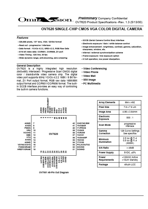
OV7620 Product Specifications -Rev. 1.3 (5/13/00)OV7620 SINGLE-CHIP CMOS VGA COLOR DIGITAL CAMERAFeatures• 326,688 pixels, 1/3” lens, VGA / QVGA format • Read out - progressive / Interlace• Data format - YCrCb 4:2:2, GRB 4:2:2, RGB Raw Data • 8/16 bit video data: CCIR601, CCIR656, ZV port • Video Timing - 525 line, 30 fps• Wide dynamic range, anti-blooming, zero smearing• SCCB (Serial Camera Control Bus) interface • Electronic exposure / Gain / white balance control• Image enhancement - brightness, contrast, gamma, saturation, sharpness, window, etc.• Internal / external synchronization scheme • Frame exposure / line exposure option • 5 Volt operation, low power dissipation.General DescriptionOV7620 is a highly integrated high resolution (640x480) Interlaced / Progressive Scan CMOS digital color / black&white video camera chip. The digital video port supports 60Hz YCrCb 4:2:2 16Bit / 8 Bit for-mat, ZV Port output format, RGB raw data 16Bit/8Bit output format and CCIR601/CCIR656 format. The built-in SCCB interface provides an easy way of controlling the built-in camera functions.• Video Conferencing • Video Phone • Video Mail • Still Image • PC MultimediaOV7001 48-Pin Out DiagramU V 7/B 8U V 6/B P C L R U V 5/M I R U V 4/S L A E N U V 3/E C L K O U V 2/Q V G A U V 1/C C 656U V 0/G A M D I S X C L K 1X C L K 2D V D D D G N D 654321484746454443A G N D V R E Q F R E X A G C E N /R A M I N T R E S E T S V D D S G N D MI D S I O -0S I O -1A V D D A G N D789101112131415161718AGND AVDD PWDN VRS VCCHGSBB VTO AVDD AGNDVSYNC/CSYS FODD/SRAM HREF/VSRAM 313233343536373839404142DOGNDDOVDD PCLK/OUTX2Y7/CS0Y6/CS2Y5/SHARP Y4/CS1Y3/RAW Y2/G2X Y1/PROG Y0/CBAR CHSYNC/BW 192021222324252627282930OV7620Array Elements 664 x 492Pixel Size 7.6 x 7.6 um Image Area 4.86 x 3.64mmElectronic Exposure500 : 1Scan Mode progressive interlace Gamma Correction 128 Curve Settings See specifics Minimum Illumination 2.5 lux @ f1.40.5 lux @ f1.4(3000K)S/N Ratio > 48dB Power Supply 5VDC, ±5% PowerRequirements <120mW Active <10uW Standby Package48-pin LCCSECTION 1PRODUCT OVERVIEWOV7620 is a highly integrated high resolution (640x480) Interlaced / Progressive Scan CMOS digital color / black&white video camera chip. The digital video port supports 60Hz YCrCb 4:2:2 16Bit / 8 Bit format, ZV Port output format, RGB raw data 16Bit/8Bit output format and CCIR601/ CCIR656 format. The built-in SCCB (Serial Camera Control Bus) interface provides an easy way of controlling the built-in camera functions.1.1 FEATURES• Single chip digital color/black&white video camera chip.• Scanning - Interlaced / Progressive Scan.• Format - 1/3” lens compatible.• Image area -4.86X 3.64mm.• Total active pixel elements - (H)664 x (V)492 square pixel.• Default active pixel element -(H)640 x (V)480.• Pixel size: 7.6 x 7.6um.• 10Bit two channel internal A/D Converter and 8/10 Bit Output.• PCLK and HREF polarity programmable.• Digital Output format -YCrCb 16bit/8bit selectable60Hz 16 Bit YCrCb 4:2:2 - 640x48060Hz 8 Bit YCrCb 4:2:2 - 640x480RGB Raw Data Digital Output 16Bit/8Bit selectable• Two-line output:• Y Channel: B G B G B G ...• UV Channel: G R G R G R ...Two-line alternate output:Y Channel: G G G G G G ...UV Channel: B R B R B R ...One-line output, use Y Channel only, effective only in Progressive Scan Mode1st line: B G B G B G B G...2nd line: G R G R G R G R ...• CCIR601 /CCIR656 standard.• YCrCB or YUV output format to support TV or monitor display• ZV Port YUV 16 Bit format.• QVGA format(320x240).• Y/UV or RGB output byte MSB and LSB swap.• SCCB interface, support fast mode: 400 kBit/s.• External Field Sync input.• External Horizontal / Vertical Sync input format, OV7620 worked as slave chip.• Support external micro-controller and RAM interface• Progressive Scan mode: support whole-frame exposure.• Programmable frame rate - 0.5 to 30fps.• Electronic shutter setting (use 27Mhz crystal and default clock rate).Interlaced: 1/60 to 1/15734(s)Progressive Scan: 1/30 to 1/15734(s)• AGC (+24dB) - auto / programmable.• PreAmp Gain 6/12 db.• Auto-Exposure-ratio programmable.• White balance - auto/programmable.• Auto-White-Balance-ratio programmable.• Brightness & contrast adjustment.• Color Saturation adjustment.• Aperture correction.• Multiple gamma correction curve selection.• Multiple luminance gamma correction curve selection.• S/N ratio > 48 dB.• Software/Hardware Reset.• Software/hardware power saving control• Minimum illumination 2.5 lux at f1.4 (3000k).• Optical fill factor is 40%.• Supply: 5 volt for analog and Digital circuit;5volt or 3.3volt for digital interface.• Power consumption < 120 mW.• Power-save mode < 10 uA.• Chip SCCB ID: 0 1 0 CS2 CS1 CS0 1 R/W (CS2 CS1 CS0 select by PIN when power-on, default 0).• 48pin package.1.2 Pin AssignmentsTable 1:Pin Descriptions(Pin type and default level: I-1: digital input+10k pull up; I-0: digital input +10k pull down, XI/XO; xtal IO; /Secondary functions are set during power up; O/I: digital CMOS level output Bias: power supply bias.).Pin #Name Class Function1 SVDD Bias Sensing Power (+5V) pins.8, 14,44AVDD Bias Analog Power (+5V) pins.29DVDD Bias Digital Power (+5V) pins.32DOVDD Bias Digital I/O Power (+5V / +3.3V) pins.48SGND Bias Sensing ground connections. Connect to supply common6, 7, 15, 43 AGND Bias Analog ground connections. Connect to supply common30DGND Bias Digital ground connection. Connect to supply common31DOGND Bias Digital Output ground connection.2RESET I Chip reset, “high” active.3AGCEN/RAMINT I-I AGCEN =1 enables the Auto Gain Control. AGCEN = 0 disables it.This pin setting is effective when pin SBB = 1.RAMINT=1 initializes frame transfer.4FREX I Frame exposure control input, effective in progressive scan only.The positive width of FREX defines the exposure time.5VrEQ CAP Internal voltage reference. Requires an 0.1uF decoupling capacitorto ground.9PWDN I-0PWDN =1 puts chip in power down (sleep) mode.10VrS CAP Internal voltage reference. Requires an 0.1uF decoupling capacitorto ground.11VcCHG CAP Internal voltage reference. Requires an 1.0uF decoupling capacitorto ground.12SBB I SBB = 1 selects the power-up method of programming the internalfunctions. SBB = 0 selects the SCCB pin programming method.Results of the power-up method can only be changed by a newpower-up or reset sequence.13VTO O Video Test Output (NTSC)16VSYNC/CSYS O/I VSYNC: Vertical sync output. This pin is asserted high during sev-eral scan lines in the vertical sync period.CSYS: Composite Sync. When not using SCCB, a 10k pull upchanges pin 42(CHSYNC) to CSYS.17FODD/SRAM O/I FODD: Odd field flag. Asserted high during the odd field, low duringthe even field.SRAM: External SRAM18HREF/VSFRAM O/I HREF: Horizontal window reference output. HREF is high during theactive pixel window, otherwise low.VSFRAM: Vertical Sync Frame.19UV7/B8O/I UV7: Digital output UV bus. UV7 used for 16-bit operation for out-putting chrominance data.B8: Switch for 8 bit mode luminance/Chroma tristate. Default is 16bit mode.20UV6/BPCLR O/I UV6: Digital output UV bus. UV6 used for 16-bit operation for out-putting chrominance data.BPCLR: Bypass RGB color matrix.21UV5/MIR O/I UV5: Digital output UV bus. UV5 used for 16-bit operation for out-putting chrominance data.MIR: Mirror.Pin #Name Class Function22UV4/SLAEN O/I UV4: Digital output UV bus. UV4 used for 16-bit operation for out-putting chrominance data.SLAEN: Slave Enable.23UV3/ECLKO O/I UV3: Digital output UV bus. UV3 used for 16-bit operation for out-putting chrominance data.ECKLO: Swap clock output - changes pin 17(FODD) to XCLK out. 24UV2/QVGA O/I UV2: Digital output UV bus. UV2 used for 16-bit operation for out-putting chrominance data.QVGA: QVGA format (320x240)25UV1/CC656O/I UV1: Digital output UV bus. UV1 used for 16-bit operation for out-putting chrominance data.CC656: CCIR 656 mode.26UV0/GAMDIS O/I UV0: Digital output UV bus. UV0 used for 16-bit operation for out-putting chrominance data.GAMDIS: Disables Chroma Gamma (RGB).27, 28XCLK1, XCLK2XO, XI XCLK1 and XCLK2 are the input/output of the on-chip video oscilla-tor. Nominal crystal clock frequency is 27MHz. If an external clock isused, input to XCLK1, leave XCLK2 unconnected.33PCLK/OUTX2O/I PCLK: Pixel clock output. By default, data is updated at the fallingedge of PCLK and is stable at its rising edge. PCLK runs at the pixelrate in 16-bit bus operations and twice the pixel rate in 8-bit busoperationsOUTX2: Doubles current output.34Y7/CSO O/I Y7: Digital output Y bus. In a 16-bit operation, the luminance data isclocked out of this bus at the rate of one byte per pixel. In 8-bit oper-ation, the luminance data and the chrominance data is multiplexedto this bus.CSO: ID configuation bit for the SCCB slave ID.35Y6/CS2O/I Y6: Digital output Y bus. In a 16-bit operation, the luminance data isclocked out of this bus at the rate of one byte per pixel. In 8-bit oper-ation, the luminance data and the chrominance data is multiplexedto this bus.CS2: ID configuation bit for the SCCB slave ID.36Y5/SHARP O/I Y5: Digital output Y bus. In a 16-bit operation, the luminance data isclocked out of this bus at the rate of one byte per pixel. In 8-bit oper-ation, the luminance data and the chrominance data is multiplexedto this bus.SHARP: Enable Analog Sharpness.37Y4/CS1O/I Y4: Digital output Y bus. In a 16-bit operation, the luminance data isclocked out of this bus at the rate of one byte per pixel. In 8-bit oper-ation, the luminance data and the chrominance data is multiplexedto this bus.CS1: ID configuation bit for the SCCB slave ID.38Y3/RAW O/I Y3: Digital output Y bus. In a 16-bit operation, the luminance data isclocked out of this bus at the rate of one byte per pixel. In 8-bit oper-ation, the luminance data and the chrominance data is multiplexedto this bus.RAW: Raw Data.39Y2/G2X O/I Y2: Digital output Y bus. In a 16-bit operation, the luminance data isclocked out of this bus at the rate of one byte per pixel. In 8-bit oper-ation, the luminance data and the chrominance data is multiplexedto this bus.G2X: Gain 2X.Pin #Name Class Function40Y1/PROG O/I Y1: Digital output Y bus. In a 16-bit operation, the luminance data isclocked out of this bus at the rate of one byte per pixel. In 8-bit oper-ation, the luminance data and the chrominance data is multiplexedto this bus.PROG: Progressive Scan Mode.41Y0/CBAR O/I Y0: Digital output Y bus. In a 16-bit operation, the luminance data isclocked out of this bus at the rate of one byte per pixel. In 8-bit oper-ation, the luminance data and the chrominance data is multiplexedto this bus.CBAR: Color Bar Test Pattern.42CHSYNC/BW O/I CHSYNC: Digital output for either composite sync or horizontal syncsignal.BW: Enables Black & White.45SIO-1I SCCB Serial clock input with schmitt trigger.46SIO-0IO SCCB Serial data, input with schmitt trigger.47MID I-0Multiple SCCB slave ID enable.MID = 1 SCCB slave ID is configurable through power up setting inCS(2:0)MID = 0 SCCB slave ID is preset to 42H/43H.1.3 CHIP OPERATIONReferring to FIG 1.1, OV7620 includes a 664x492 resolution image array, an analog signal pro-cessor, dual 10bit A/D converters, analog video mux, digital data formatter and video port, SCCB interface with its registers, the digital controls including timing block, exposure block and white balance.FIG 1.1 OV7620Block DiagramOV7620is a 1/3 inch CMOS imaging device. The sensor contains approximately 326,688 pixels.It is base on field integration read-out system with line-by-line transfer and an electronic shutter with synchronous pixel read out scheme. The color filter of the sensor consists of primary color RG/GB array arranged in line alternating fashion.RVO BUO GYOimage r o w s e l e c tcolumn sense amparrayCb CrY VcSAT GAMMAwhiteexposure detect WB controlbalancedetectAWBAGCENXVCLK1(664X492)RGB1/2sys-clkAWBTH/VcCNTr g bmxFODDVSYNCHREFPCLK video timing generatorFZEXexposurecontrolVrEQVcSHPFREZCHSYNCmxADCf o r m a t t e rY(7:0)UV(7:0)SCCBinterfaceSIO-1SIO-0registersv i d e o p o r tADCanalog processingFSIN MIR DENBmxPROGAWBTMSBBThe majority of signal processing is performed in the analog processing block, which does color separation, matrixing, AGC, gamma correction, color correction, color balance, black level cali-bration, knee smooth, aperture correction, controls for the luminance and chrominance picture and anti-alias filtering. The analog video signals are based on the formula:Y = 0.59G + 0.31R + 0.11B; where R,G,B is the equivalent color components in each pixelU = R-Y;V = B-Y;Another output data format is YCrCb, its formula is as follows:Y = 0.59G + 0.31R + 0.11BCr = 0.713 x (R - Y)Cb = 0.564 X (B - Y)The YCrCb /RGB Raw Data signal is fed to two 10 bit A/D converters, one for the Y/R&G chan-nel, one is shared by Cr&Cb / B&G channels. The A/D converted data stream is further condi-tioned in the digital formatter, finally the 16bit or 8 bit data muxing is done in the digital video port.The on-chip 10 bit A/D can operate up to 13.5 MSPS, since it is fully synchronous to the pixel rate, the conversion rate always follows the frame rate. An A/D black-level-calibration circuitry ensures the black level of Y/RGB is translated to value 16, and the peak white level is limited to 240; CrCb black level is 128, Peak/Bottom is 240/16. RGB raw data output range is 16/240, 0 & 255 reserved for sync flag. Also OV7620 support non-CCIR standard output range, that is 1/254, 0 and 255 are reserved for sync flag.The computation in the electronic exposure control is based on the brightness of the full image. The exposure algorithm is optimized for normal scene which assuming the subject is well-lit rel-ative to the background. In case of a different backlight condition, there is also a AEC White/ Black ratio selection register, which can be used as AEC algorithm adjustment to get special im-age. Along with the AEC is the on chip AGC which can boost gain up to 24dB if needed. To achieve proper color temperature, auto or manual white balance control is also available. There is a separate saturation, brightness contrast and sharpness adjustment for further fine tuning of the picture quality. OV7620 provide a set of register to control White Balance ratio register which can be used as increase/decrease image field Red/Blue component ratio. In most case, the de-fault setting may be sufficient.The windowing feature allows the user to size the window according to their need. The window is sizable from 4X2 to 664x492 and can be placed anywhere inside the 664X492 boundary. Not-ed this function does not change the frame rate or data rate, it simply change the assertion of the HREF to match with the horizontal and vertical region that is programmed by the user. A typical application for this is hardware zooming, and panning. Default output window is 640x480.The digital video port offers 16 bit 4:2:2 format complying to the 60Hz CCIR601 timing standard. OV7620 also supports 8 bit data format in Cb Y Cr Y order by using port Y only and running at twice the pixel rate while the port UV is inactive. Other than the 16 bit data bus, OV7620 supplies standard video timing signals such as VSYNC, HREF, PCLK, FODD, CHSYNC.OV7620 support standard ZV Port Interface Timing. It provides VSYNC, CHSYNC, PCLK and 16 Bit data bus: Y<7:0> and UV<7:0>. PCLK rising edge clock data bus into ZV port.To decrease data transfer rate while high resolution image unnecessary, OV7620 provide a so-lution, that is it can output QVGA resolution image. This mode decrease pixel rate one half. The resolution default value is 320x240 and can be programmable. Every line only output one half data. For Interlaced Mode, all field line output (320), for Progressive Scan Mode, only one half line data output.The digital video port also offer RGB Raw Data 16 Bit/8 Bit format. The output sequence is matched to OV7620 Color Filter Pattern, that is UV channel output sequence is G R G R ..., Y Channel output sequence is B G B G,....To 8 Bit RGB Raw data output format, just use Y channel and disable UV channel, output sequence is B G R G ....OV7620 support CCIR656 YCrCb 4:2:2 digital output format. The SAV(Start of Active Video) and EAV(End of Active Video) is just at the beginning and the end of HREF window. So the position of SAV and EAV is changing with active pixel window. Also you can get 8 bit RGB raw data with SAV and EAV information.OV7620 support some flexible YUV output format. One is standard YUV 4:2:2. Another is U V sequence swap format, that means UV channel output V U V U ...(16 Bit) and V Y U Y ...(8 Bit). The 3rd format is Y/UV sequence swap in 8 Bit output, that is Y U Y V ....OV7620 can be use as black&white camera. At this mode, it’s vertical resolution will be higher than color mode. All data will be output from Y port and UV port will be tri-state. Data (Y/RGB) output rate is same as 16 Bit mode.OV7620 can be programmable to swap Y/UV or RGB output byte MSB and LSB. Y7 - Y0 default sequence is Y7 is MSB and Y0 is LSB. When swap, Y7 is LSB and Y0 is MSB, relative middle bits are swapped.An important factor about digital camera is how convenient the interface is, OV7620 has made the frame rate programmable and the A/D synchronous to the actual pixel rate. Essentially, it is a whole image capture system in a single chip. Since the internal AEC has a range of 1:260, and AGC have 24dB, for the most of applications, the camera can adjust itself to meet the lighting condition without user intervention.OV7620 support hardware/software RESET function: when RESET pin tie to high, whole chip will be reset including all register. Hardware sleeping mode: when PWDN tie to high, chip clock will be stop and internal circuit reset except all SCCB register. Also there is a SCCB control soft-ware reset control register 12 bit 7, which is same as hardware RESET pin function.OV7620 hardware reset time minimum is 1 ms.OV7620 support hardware/software power saving mode. When the PWDN pin tie to high, whole chip will be set to power down status without any current consumption. For software power down control, all current set to zero except crystal circuit. In power down mode, all SCCB register value will be kept.Two control mechanism have been built into OV7620: A. one time read-in of pin states at power up or RESET status, including hardware and software reset; B. SCCB interface. Two methods are mutually exclusive, only one is used at a time, selected by pin SBB. Method A has limited access to full chip features.The power up reset method is a one time setting, the setting can not be altered later. The pinsused in the control are shared with the digital video port data bus. At power up, the video port is initially tri-stated, allowing the external pull-up/pull-down resistor to set the default operating con-ditions, 2048 clocks later the video port resumes normal function. The detail of the power up pin control method is explained in the individual pin out section.SCCB interface provides full access to all the features. The detail is in the SCCB register set.1.4 VIDEO FORMATTable 1.1: 4:2:2 16 bit FormatData Bus Pixel Byte SequenceY7Y7Y7Y7Y7Y7Y7Y6Y6Y6Y6Y6Y6Y6Y5Y5Y5Y5Y5Y5Y5Y4Y4Y4Y4Y4Y4Y4Y3Y3Y3Y3Y3Y3Y3Y2Y2Y2Y2Y2Y2Y2Y1Y1Y1Y1Y1Y1Y1Y0Y0Y0Y0Y0Y0Y0UV7U7V7U7V7U7V7UV6U6V6U6V6U6V6UV5U5V5U5V5U5V5UV4U4V4U4V4U4V4UV3U3V3U3V3U3V3UV2U2V2U2V2U2V2UV1U1V1U1V1U1V1UV0U0V0U0V0U0V0Y FRAME012345UV FRAME024Table 1.2: 4:2:2 8 bit FormatData Bus Pixel Byte SequenceY7U7Y7V7Y7U7Y7V7Y7 Y6U6Y6V6Y6U6Y6V6Y6 Y5U5Y5V5Y5U5Y5V5Y5 Y4U4Y4V4Y4U4Y4V4Y4 Y3U3Y3V3Y3U3Y3V3Y3 Y2U2Y2V2Y2U2Y2V2Y2 Y1U1Y1V1Y1U1Y1V1Y1 Y0U0Y0V0Y0U0Y0V0Y0 Y FRAME0123 UV FRAME0 1 2 3FIG 1.2 Pixel Data Bus (YUV Output)Note: Tclk is pixel clock period. When OV7620 system clock is 27MHz, Tclk=74ns for 16 Bit out-put; Tclk=37ns for 8 Bit output. Tsu is HREF set-up time, maximum is 15 ns; Thd is HREF hold time, maximum is 15 ns.Y<7:0>PCLKHREFUV<7:0>1010YY8080U V repeat for all data bytesPixel Data 16 bit TimingY<7:0>PCLKHREFrepeat for all data bytesPixel Data 8 bit TimingU Y V Y 80101080Use PCLK rising edge latch data busUse PCLK rising edge latch data busTsuThdThdTclkTclk10Tsu1.5 RGB Raw Data FormatRGB Raw data output from Y and UV port.UV port output data sequence: G R G R G R ... or B R B R ...(refer to register 28 bit 2)Y port output data sequence: B G B G B G ... or G G G G ...(refer to register 28 bit 2)Array Color Filter Patter is Bayer-PatternTable 1.3:R\C1234.6416426436441B11G12B13G14B G B G2G21R22G23R24G R G R3B31G32B33G34B G B G4G41R42G43R44G R G R5B51G52B53G54B G B G.481B G B G B G B G482G R G R G R G R483B G B G B G B G484G R G R G R G R485B G B G B G B G1.5.1 Interlaced Mode 16 Bit Format (HREF total 242)1.5.1.1 Default mode: In ODD FIELD, 1st HREF output UV channel is 2nd line: G21 R22 G23 R24... and Y channel is Row 1: B11 G12 B13 G14 ... . 2nd HREF output UV channel output 4th line: G41 R42 G43 R44 ... and Y port output 3rd line: B31 G32 B33 G34 ... , so on. Data bus should be latched by PCLK rising edge and related to the exact phys-ical position In Even FIELD, 1st HREF Y channel output B31 G32 B33 G34 ... and UV channel output G21 R22 G23 R24 ...2nd HREF Y channel output B51 G52 B53 G54 ... and UV output G41 R42 G43 R44 ....1.5.1.2 YG mode: In ODD FIELD, 1st HREF Y channel output G21 G12 G23 G14 ... and UV channel is B11 R22 B13 R24 .... 2nd HREF Y channel output G41 G32 G43 G34 ... and UV channel output B31 R42 B33 R44 .... In EVEN FIELD, 1st HREF Y channel output G21 G32 G23 G34 ... and UV channel output B31 R22 B33 R24 ... 2nd HREF channel output G41 G52 G43 G54 ... and UV channel output B51 R42 B53 R44 ...1.5.2 Progressive Scan Mode 16 Bit Format (HREF total 484)1.5.2.3 Default mode: 1st HREF UV channel output unstable data, Y output B11 G12 B13 G14 .... 2nd HREF UV channel output G21 R22 G23 R24 ..., Y output B11 G12 B13 G14 ... 3rd HREF UV channel output G21 R22 G23 R24 ..., Y output B31 G23 B33 G34 .... Every line data output twice.1.5.2.4 YG mode: 1st HREF Y and UV output unstable data. 2nd HREF Y channel output G21 G12 G23 G14 ..., UV output B11 R22 B13 R24 ... 3rd HREF Y is G21 G32 G23 G34 ..., UV channel is B31 R22 B33 R24 ... Every line data out-put twice.1.5.2.5 One line mode: 1st HREF Y channel output B11 G12 B13 G14 ..., 2nd HREF Y channel output G21 R22 G23 R24 ..., so on. UV channel tri-state.1.5.3 Interlaced Mode 8 Bit (242 HREF)1.5.3.6 ODD FIELD: 1st HREF Y channel output B11 G21 R22 G12 ... 2nd HREF Y channel output B31 G41 R42 G32..., so on. PCLK timing is double and use PCLK rising edge latch data bus. UV channel tri-state.1.5.3.7 EVEN FIELD: 1st HREF Y channel output B31 G21 R22 G32 ... 2nd HREF Y channel output B51 G41 R42 G52 ..., so on. PCLK timing is double and data bus should be latched by its rising edge. UV channel tri-state.1.5.4 Progressive Scan Mode 8 Bit (484 HREF)1.5.4.8 1st HREF Y channel output unstable data. 2nd HREF Y channel output B11 G21 R22 G12 ... 2nd HREF Y channel output B31 G21 R22 G32 ..., so on. PCLK timing is double and PCLK rising edge latch data bus. UV chan-nel tri-state. Every line data output twice.RGB raw data timing chart is as follows:FIG 1.3 Pixel Data Bus (RGB Output)Note: Tclk is pixel clock period. When OV7620 system clock is 27MHz, Tclk=74ns for 16 Bit out-put; Tclk=37ns for 8 Bit output. Tsu is HREF set-up time, maximum is 15 ns; Thd is HREF hold time, maximum is 15 ns.UV<7:0>PCLKHREFY<7:0>1010GR1010B G repeat for all data bytesPixel Data 16 bit TimingY<7:0>PCLKHREF1010BBrepeat for all data bytesPixel Data 8 bit Timing10GG10PCLK rising edge latch data busPCLK rising edge latch data busTclkTclkThdThdTsuTsu1.6 ZV Port Interlace TimingThe ZV Port is a single-source uni-directional video bus between a PC Card socket and a VGA controller. The ZV Port complies with CCIR601 timing to allow NTSC decoders to deliver real-time digital video straight into the VGA frame buffer from a PC Card. OV7620 support ZV Port Timing, which output signal can be output to a PC Card directly, then to VGA controller. The tim-ing is as below:FIG 1.4 ZV Port TimingNotes: ZV Port format output signal include:VSYNC : Vertical sync pulse.HREF : Horizontal valid data output window.PCLK : Pixel clock used to clock valid data and CHSYNC into ZV Port. Default frequency is 13.5MHz whenuse 27MHz as system clock. Rising edge of PCLK is used to clock the 16 Bit data.Y<7:0>: 8 Bit luminance data bus..UV<7:0>: 8 Bit chrominance data bus.All Timing Parameters is list in following table.‘VSYNCPCLKY<7:0>UV<7:0>/HREF639640t8t8Even Field 1(FODD=0)Odd Field(FODD=1)t6t7t1t2t3t4Horizontal TimingVSYNCY<7:0>/UV<7:0>Valid Data1 Line TvsTve t5Tline12Table 1.4: ZV Port AC ParameterSymbol Parameter Min.Max.t1PCLK fall timing 4 ns8 nst2PCLK low time30 nst3PCLK rise time 4 ns8 nst4PCLK high time30 nst5PCLK period74 nst6Y/UV/HREF setup time10 nst7Y/UV/HREF hold time20 nst8VSYNC setup/hold time to HREF 1 usNote: In Interlaced Mode, there are Even/Odd field different (t8). When In Progressive Scan Mode, only frame timing same as Even field(t8).After VSYNC falling edge, OV7620 will output black reference level, the line number is Tvs, which is the line number between the 1st HREF rising edge after VSYNC falling edge and 1st valid data CHSYNC rising edge. Then valid data, then black reference, line number is Tve, which is the line number between last valid data CHSYNC rising edge and 1st CHSYNC rising edge after VSYNC rising edge. The black reference output line number is dependent on vertical win-dow setting.When in default setting, Tvs = 14*Tline, which is changed with register register 19<7:0>. If in Interlaced Mode, register 19<7:0> change 1 step, Tvs increase 1 line. If in Progressive Scan Mode, register 19<7:0> step equal to 2 line.When in default setting, Tve = 4*Tline for Odd Field, Tve = 3*Tline for Even Field, which is changed with register register 1A<7:0>. If in Interlaced Mode, register 1A<7:0> change 1 step, Tve increase 1 line. If in Progressive Scan Mode, register 1A<7:0> step equal to 2 line.In Progressive Scan Mode, Tve = 3*Tline and Tvs = 35*Tline.1.7 Interface for External RAM Controller and Micro-controllerOV7620 can be programmed to output single frame data to external RAM. The structure block diagram is as follows:The timing diagram is as follows:OV7620FPGA u-CPUDRAM / SRAMDataAddACK SCCB and InitialSRAM DATAHREF VS AGCEN Tri-StateTri-State。
单片机控制摄像头摄像、显示系统111

单片机控制摄像头摄像、显示系统1111 单片机控制摄像头摄像、显示系统系别尚德光伏学院专业微电子技术班级 0801 学生姓名丁良林学号 100080253 指导教师陆亚青 2011年 4 月无锡科技职业学院毕业设计论文单片机控制摄像头摄像、显示系统 1 单片机控制摄像头摄像、显示系统摘要本项目主要是通过是S12XS128单片机来控制摄像头的正常工作并由该单片机送到电脑上。
其实很简单就是通过单片机来控制摄像头来拍照然后单片机再将拍摄到的图片传输到电脑上显示让人眼能看到所拍摄的画面。
所选的MC9S12XS128 单片机产品满足了用户对设计灵活性和平台兼容性的需求并在一系列汽车电子平台上实现了可升级性、硬件和软件可重用性、以及兼容性。
它为用户削减了成本并缩小了封装尺寸。
该项目在很多领域都有广泛的应用例如大学生智能车制作和监控系统。
例外选的OV7620是一款CMOS摄像头器件是一款彩色CMOS 型图像采集集成芯片提供高性能的单一小体积封装该器件分辨率可以达到640X480传输速率可以达到30帧。
关键词MC9S12XS128单片机OV7620摄像头显示系统无锡科技职业学院毕业设计论文单片机控制摄像头摄像、显示系统 2 abstract Abstractthis project mainly through is S12XS128 single shipcontrolling of the camera normal work and by the single-chip microcomputer to computer. Actually very simple is through the single ship controlling camera to take photos and then again to photograph of single-chip computer images transmitted to display on let the human eye can see the picture taken. Selected MC9S12XS128 microcontroller products meet the user to design flexibility and platform compatibility needs and in a series of automobile electronic platform achieved scalability the hardware and software reusability and compatibility. It for the user cut costs and reduce the encapsulation size. This project in many fields are widely used such as college students intelligent car production and monitoring system. Exception chosen OV7620 is a section CMOS camera device is a new color CMOS type image acquisition integrated chips to supply high-performance single small volume encapsulation this device resolution can achieve 640X480 transmission rate can reach 30 frames. Key wordsMC9S12XS128 microcontroller OV7620 cameras the display system. 无锡科技职业学院毕业设计论文单片机控制摄像头摄像、显示系统 3 目录前言 ................................................................. .................................................................................. 1 第一章系统的结构和功能现象 ................................................................. .................................... 1 11 系统的总体结构 ................................................................. ............................................ 1 1.2功能及现象 ................................................................. ....................................................... 2 第二章飞思卡尔XS128单片机介绍 ..................................................................... ........................ 1 2.1 XS128特性与封装 ................................................................. ........................................... 1 2.2单片机和相关引脚介绍 ..................................................................... ............................... 3 第三章OV7620摄像头 ..................................................................... ...............................................1 3.1 OV7620各模块介绍 ................................................................. ......................................... 1 3.1.2本摄像头模块新增特点 ..................................................................... ....................... 1 第四章单片机的连接与编程 ..................................................................... .................................... 2 4.1XS128最小系统 ..................................................................... ...........................................2 4.2 XS128与OV7620的硬件连接 ................................................................. ......................... 2 4.3 MC9S12XS128最小系统测试程序 ..................................................................... ............... 1 4.4 摄像头摄像及PC显示程序 ..................................................................... ........................ 2 总结 ..................................................................... .............................................................................. 2 致谢 ................................................................. .................................................................................. 1 参考文献 ................................................................. ........................................................................ ..1 附录 ................................................................. ................................................................................ 2 无锡科技职业学院毕业设计论文单片机控制摄像头摄像、显示系统 1 前言我们本次设计主要功能是用MC9S12XS128单片机来控制摄像头OV7620的正常工作并且在电脑上显示接受的图像和数据也就是通过XS128单片机输出摄像头采集到的图像经PC串口在电脑上的上位机软件上显示。
ov7620摄像头

新推出基于OV7620的C3188模块,ov7620和ov6620类似,外围电路完全相同,不同在于ov7620用27M 晶振,ov6620用17.7344M晶振,不同之处在于OV7620最大分辨率是640*480,所谓VGA模式,而OV6620只有288*352,即CIF模式,第二不同是ov6620只有progressive scan(逐行扫描),ov7620既有progressive scan(逐行扫描),还Interlaced scan (隔行扫描)。
由于两者的外围电路一样,所以我的电路板还是原来的板即可对于智能车来说,只需用ov6620默认的YUV模式,取Y0~Y7的亮度值(也就是识别黑白线),接单片机的GPIO就可以了;另外就是Vsync表示一帧数据来,低电平有效,一般接单片机的外部下降沿中断,也可以上升沿中断,当然需要其他外围电路了;Href表示一行行,高电平有效,一般也接单片机外部中断;Pclk 表示一个像素点的到来.关于ov6620的寄存器来说,datasheet上说是SCCB 协议,吓坏了一大堆人,其实就是I2C协议,唯一的不同就是SCCB读寄存器的话一定要插入一个写寄存器,很多用户会用单片机的GPIO来模拟SCCB我觉得没有必要,有了现成I2C就可以了,SDA和SCL接两个上拉电阻,我自己就是用I2C来做的。
当然智能车只用默认模式就好了,我是要用RGB模式才需要配置寄存器的。
以上就是ov6620最重要的两点了,当然其他问题我一定给大家最大的技术支持,看下面就知道了。
智能车只要采集所谓的几行亮度数据,从某种程度上说,根本无需对ov6620的寄存器进行配置,而ov6620最关键的两点是:一是寄存器配置,二是Vsync,Href,Pclk三者的时序,或许很多玩智能车的人只是对第二个很熟悉,而对第一重要点就不是很了解了。
如果你掌握以上两点,你想怎么玩ov6620就怎么玩,我可以给大家提供帮助,你就不仅仅只会玩智能车了,还学到了更多的东西,也不会只有黑白的世界了。
Ov7620的参数,调焦,硬件接法,采集图像,及图像处理
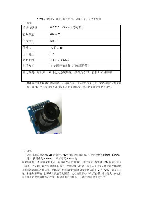
Ov7620的参数,调焦,硬件接法,采集图像,及图像处理一、参数图像传感器Ov7620,1/3 cmos感光芯片有效像素640*480信号制式NTSC信噪比大于48db工作电压+5V感光面积 4.86 x 3.64mm扫描方式支持隔行和逐行(可编程设置)应用案例:智能车、双目视觉系统研究、摄像头学习、自制照相机等等其中有效像素我们在实际跑道上不用这么多,因为它数据量太大,规定用的芯片最大内存只有8k,所以我们需要在扫描的时候采取隔行扫描,这个在后续中会讲到。
二、调焦调焦所用的设备为:usb采集卡。
7620的焦距是固定的,有不同规格(3.6mm,2.8mm,等),我买的是3.6mm,一般都是配3.6mm的。
调焦会用到USB 视频采集卡和一根带莲花头的测试线,调试方法:首先将USB 视频采集卡一端插在已安装好软件和驱动的电脑上,视频采集卡的另一端有四个接头,其中黄色视频接口接在测试线的莲花头端;测试线有杜邦线的一端分别接摄像头的VTO 和GND,摄像头上电并和采集棒共地,打开软件就能看到图像。
这时按照顺时针或者逆时针拧动镜头,在软件中看图像知道最清晰停止拧动,用螺丝刀固定镜头上小螺丝即完成调焦工作。
三、硬件连接上图为调焦用的。
当在采集图像的时候,根据各自的情况选择要的端口。
我在采集图像的时候采用的是href(行中断),vsyn(场中断),和8位xs128芯片的普通I/O口。
四、图像采集由于xs128芯片没有串口接口,所以我采用了usb转串口模块,把电脑上的发送电平转成xs128芯片所识别的ttl电平。
这样就可以让电脑和芯片之间的通信构成连接。
USB转串口使用时仅需三个引脚,分别是GND,TXD,RXD,GND接单片机的GND,TXD接单片机的RXD即P3^0,RXD接单片机的TXD即P3^1(这是51单片机),要是xs128的话,有两对收发口,分别为s0,s1和s2,s3。
硬件部分接好后,就可以打开串口调试助手。
OV7620中文寄存器
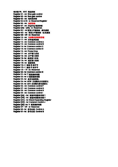
寄存器00:AGC增益控制Register01-rw:Blue gain controlRegister02-rw:Red gain controlRegister03-rw:饱和度控制Register04&05-w:Reserved Register Register06-rw:亮度控制Register07-rw:Angalog锐度控制Register[08]~[0B]-w:Reserved.Register0C-rw:背景白平衡控制-蓝色通道Register0D-rw:背景白平衡控制–红色通道0F--rw:ReservedRegister0E~0FRegister10-rw:自动曝光控制寄存器Register11-rw:时钟速率控制Register12-rw:Common control A Register13-rw:Common control B14--rw:Common control C Register1415--rw:Common control D Register15Register16-rw:Frame DropRegister17-rw:水平窗口启动Register18-rw:水平窗口结束Register19-rw:垂直窗口启动Register1A-rw:垂直窗口结束Register1B-rw:像素转换Register1C-r:制造ID高字节Register1D-r:制造ID低字节1F--rw:ReservedRegister1E~1F20--rw:Common control E Register2021--rw:Y通道偏移调整Register21Register22-rw:U通道偏移调整Register23-rw:晶体电流控制。
Register24-rw:AEW自动曝光白色像素比25--rw:AEC自动曝光黑色像素比Register25Register26-rw:Common control F Register27-rw:Common control G Register28-rw:Common control H Register29-rw:Common control IRegister[2A]-rw:帧速率调整寄存器1 Register[2B]-rw:帧速率调整寄存器2 Register[2C]-rw:Black Expanding Register Register[2D]-rw:Common Control J Register[2E]-rw:V通道偏移调整Register2F~5F-w:ReservedRegister6060--rw:信号处理Control A61--rw:信号处理Control B Register6162--rw:RGB Gamma ControlRegister62Register6363--rw:Reserved64--rw:Y Gamma ControlRegister6465--rw:信号处理Control CRegister6566--rw:AWB过程控制Register6667--rw:颜色空间选择Register6768--rw:信号处理Control DRegister6869--rw:模拟锐度Register696A--rw:垂直边缘增强控制Register6ARegister6B6B--6E rw:ReservedRegister6F-rw:偶/奇噪声补偿控制Register70-rw:Common Control KRegister71-rw:Common Control JRegister72-rw:水平同步第一边移Register73-rw:水平同步第二边移Register74-rw:Common Control MRegister75-rw:Common Control NRegister76-rw:Common Control ORegister77-7B-rw:ReservedRegister7C-rw:Field Average Level Storage寄存器00:AGC增益控制AGC<5:0>-增益设置为整个图像通道计算公式为:Gain=(AGC<3:0>/16+1)*(AGC<4>+1)*(AGC<5>+1);range(1x~7.75x),AGC<5>and AGC<4>control SA2.寄存器3:饱和度控制SAT<7:0>-saturation adjustment(饱和度调整)for the UV channel based on the default setting;80],减少SAT<<7:0>7:0><[<[<[80]范围(-4dB〜+6dB)。
ov7620介绍
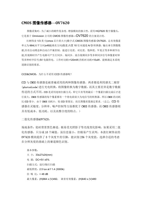
CMOS图像传感器---OV7620图像采集时,为了减小的硬件复杂度,增强模块的独立性,采用HQ7620数字摄像头,它是基于Omnivsion公司的CMOS图像传感器---OV7620的方案设计的。
红树伟业1/3英寸(cmos芯片的大小)数字式CMOS图像传感器OV7620,总有效像素单元为664(水平方向)x492(垂直方向)像素;内置10位双通道A/ D转换器,输出8位图像数据;具有自动增益和自动白平衡控制,能进行亮度、对比度、饱和度、Y校正等多种调节功能;其视频时序产生电路可产生行同步、场同步、混合视频同步等多种同步信号和像素时钟等多种时序信号;5V电源供电,工作时功耗<120mW,待机时功耗<10uW。
能够满足本系统道路识别的要求。
CCD&CMOS:为什么不采用CCD传感器呢?CCD与CMOS传感器是被普遍采用的两种图像传感器,两者都是利用感光二极管(photodiode)进行光电转换,将图像转换为数字数据,而其主要差异是数字数据传送的方式不同。
CCD是采用连续扫描方式,即它只有等到最后一个像素扫描完成后才进行放大;CMOS传感器的每个像素都有一个将电荷放大为电信号的转换器。
所以CMOS的功耗比CCD要小。
由于CMOS功耗小,较CCD要便宜,而且图像质量满足要求。
(总之:CCD传感器在灵敏度、分辨率、噪声控制等方面都优于CMOS传感器,而CMOS传感器则具有低成本、低功耗、以及高整合度的特点。
)二值化传感器&OV7620:场地条件:瓷砖背景黑色赛道,极易受光照影子等光线变化影响,如果采用二值化传感器,只分成10个阈值,虽信息量小,但极易产生误判,本款红树伟业的OV7620模块提供了8个灰度Y的引脚,能识别256个灰度值,选择合适的考虑在分辨灰度的基础上的赛道颜色识别。
基本参数:大小:33x27x24(mm)电源:DC+5V ±5%扫描方式:逐行/隔行扫描最低照度:2.5 lux at f1.4 (3000k)信噪比:> 48 dB最大像素:(H)664 x (V)492;缺省有效像素:(H)640 x (V)480工作时功耗<120mW,待机时功耗<10uW;内置10位双通道A/ D转换器;输出8位图像数据;数据输出格式:YCrCb 16bit/8bit selectable:60Hz 16 Bit YCrCb 4:2:2 - 640x48060Hz 8 Bit YCrCb 4:2:2 - 640x480摄像头主要的采样格式有YCbCr 4:2:2(Y0 U0 Y1 V1 Y2 U2 Y3 V3 )、YCbCr 4:2:0(一行是4:2:0的话,下一行是4:0:2)、YCbCr 4:1:1(水平方向上对色度进行4:1抽样)和 YCbCr 4:4:4(三个分量信息完整)。
于cmos图像传感器的usb接口图像采集系统设计

于CMOS图像传感器的USB接口图像采集系统设计介绍以C PLD控制为核心的CMOS图像采集系统,系统选用彩色图像传感器OV7620,并通过USB接口以类似DMA方式进行快速的图像传输。
最后给出了单片机固件程序和设备驱动程序的实现方法。
关键词:CMOS图像传感器;图像采集;C PLD;USBDesign of USB Image C ollecting System Based on C MOS Image SensorJIANG Chuangui, LIAO Qizhen, WEI Shimin(Automation School of Beijing University of Post and Telecommu nication, Beijing 100876, C hina)Key words: C MOS image sensor; image collection; C PLD; USB1系统设计图1为图像采集系统的原理框图。
系统选用OminiVision公司生产的C MOS芯片OV7620,它是一款集成了一个64 0×480(30万像素)图像矩阵的彩色摄像芯片,在隔行扫描模式下工作频率可达60Hz,逐行扫描时为30帧/s。
其像面大小为1/3英寸,支持8位或16位数字信号从单通道或双通道输出,输出信号的类型可在YCrCb和RGB之间选择,图像矩阵支持VGA或C IF规定,数字输出格式遵循CCIR601,ZV Ports,CCIR656等标准。
OV7620有很强的摄像和控制功能,如暴光控制,γ校正,增益,色彩矩阵,窗口选择等,所有这些功能都可以通过I2C接口进行编程控制。
2.1OV7620的输出特性OV7620工作方式和输出格式非常多,可以适应不同的应用场合,针对我们的较小系统,采用了单通道Y输出,以及逐行扫描的工作方式。
这些工作方式的实现是通过MC U的I2C编程控制的。
OV7620 cmos摄像头的使用
OV7620 cmos摄像头的使用
OV7620简介ov7620是一款CMOS摄像头器件,是彩色CMOS型图像采集集成芯片,提供高性能的单一小体积封装,该器件分辨率可以达到640X480,传输速率可以达到30帧。
OV7620是1/3”CMOS彩色/黑白图像传感器。
它支持连续和隔行两种扫描方式,VGA与QVGA两种图像格式;最高像素为664×492,帧速率为30fps;数据格式包括YUV、YCrCb、RGB三种,能够满足一般图像采集系统的要求。
OV7620基本参数大小:33x27x24(mm)
电源:DC+5V±5%
扫描方式:逐行/隔行扫描
最低照度:2.5luxatf1.4(3000k)
信噪比:》48dB
最大像素:(H)664x(V)492;缺省有效像素:(H)640x(V)480
数据输出格式:
YCrCb16bit/8bitselectable
60Hz16BitYCrCb4:2:2-640x480
60Hz8BitYCrCb4:2:2-640x480
RGBRawDataDigitalOutput16Bit/8Bitselectable
CCIR601,CCIR656,ZV端口:支持8/16位视频数据
SCCB接口:最大速率支持400kBit/s
YCrCB或YUV输出格式:支持TV或监视器显示
摄像头工作原理按一定的分辨率,以隔行扫描的方式采集图像上的点,当扫描到某点时,就通过图像传感芯片将该点处图像的灰度转换成与灰度一一对应的电压值,然后将此电压值通过视频信号端输出。
具体而言(参见图5-1),摄像头连续地扫描图像上的一行,则输。
OV7620摄像头模块 数字摄像头
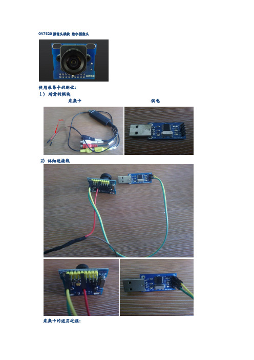
OV7620摄像头模块数字摄像头使用采集卡的测试:1)所需的模块采集卡供电2)详细连接线采集卡的运用过程:1)在桌面上找到下面的软件双击运行2)观察下面窗口的图像3)焦距的调节使用采集卡测试过程中要注意观察画面上是否有黑点,条纹,水滴,灰尘等细节。
上位机测试:所需模块:X128的烧写器CH340X128接线:S0(单片机上的RXD) -----> 串口模块TXDS1(单片机上的TXD) -----> 串口模块RXDGND(单片机上的地) -----> 串口模块GND //如果单片机和串口使用不同电源,也需要共地A0-A7 -----------------> 摄像头模块(数据)Y0 - Y7T0 -----------------> 摄像头模块(行中断)HREFT1 -----------------> 摄像头模块(场中断)VSYN详细接线图片:程序烧写的连接图程序在:胡良工作资料\测试程序\OV7620摄像头9SXS128例程详细步骤:1)在桌面找到下图图标双击打开;2)找到下图双击打开测试程序3)找到下图双击打开(OV7620摄像头9SXS128例程)4)找到下图双击打开Project.mcp5)按下图标注的序列号依次点击6)烧写过程1.2.3.4.关闭上面的那个窗口。
7)上位机的使用(在第3步后可以看到下图。
即TSL1401 9SXS128例程(线性CCD)文件下)1.2.3.4.5.6.观看窗口1和窗口2 的图像变化看最终二值化后的图片边沿是否干净。
如果没有什么干扰点则该模块的性能很好。
国外开源的OV7620使用报告

Digital Project Digital Camera Interface I˜n aki Navarro OizaMay2004AbstractThis document describes the development of a prototype of an interface between a CMOS camera and a computer.This interface allows a user to get images from the camera,to change some of the properties of the camera as brightness, luminance,etc.In addition some image process is implemented allowing the camera to track white objects and follow them with a servomotor.The interface was implemented using the Atmel AVR ATmega16microcontroller.This document is afinal report of the course Digital Project of LTH(Lunds Tekniska hogskola)Sweden.This report and information related to this project can be found in /inaki/dproject1Contents1Introduction31.1Background (3)1.2Specifications (3)2Description of the system52.1The C3088Camera (5)2.2Hardware (7)2.2.1Reset and Clock (7)2.2.2JTAG ICE (7)2.2.3LED and switch (7)2.2.4Serial communications (9)2.2.5C3088Camera (9)2.2.6Servo (10)2.2.7Comments (10)2.3Software (10)2.3.1Serial Communications (10)2.3.2I2C Communication with the camera (11)2.3.3BMP (12)2.3.4Getting Image from the Camera (13)2.3.5Little Image”Process” (13)2.3.6Servo (14)2.3.7Main (15)3Results163.1Conclusions (20)A Schematic21B Images23C Photos of the system292Chapter1Introduction1.1BackgroundFor the last four years I have been designing and building mobile robots based in microcontrollers.In this course on Digital Project I wanted to do something about robotics,but developing a robot would have been very expensive and hard in the mechanical aspects.I decided to work with something related with robotics but cheaper and in someway easier:the interface with a digital camera that later I could add to one of my robots.I own a the digital camera C3088[1].This camera is used in the CMUcam[2] interface to take images,process them and extract some interesting features that can be used by a robot.My idea was to reproduce the similar characteristics of the CMUcam using the C3088camera.I wanted that my interface would be able to get images from the camera,change the different settings of the camera (luminance,brightness,etc.),and if possible make some processing of the image (like detecting colors or lines),in a similar way as the CMUcam does.Also I had the opportunity to use the AVR ATmega16[3]microcontoller and learn about it.I decided to work with it despite it was thefirst time it was used in the course.1.2SpecificationsThe aim of the project is the design and construction of an interface between the CMOS camera c3088and a computer,using the AVR microcontroller.The informationflows in two ways:on the one hand there are commands from the computer to the camera to change different characteristics of it,on the other images from the camera should be sent to the computer.The communication between the computer and the AVR is through the serial port.The communi-cation between the camera and the microcontroller is:using the I2C protocol3to access to the different registers of the camera;and using an8bit port to read the images.In addition the camera will be connected to a TV with its analog output for debugging purpose.In the next diagram of Figure1.1we can see the main blocks of the design and how informationflows.Figure1.1:Blocks and informationflow.The proposed tasks for the project are the next:•Make the AVR ATmega16and its environment work•Communicate the AVR ATmega16with the computer•Make the camera work and see images in the TV•Read and write the registers of the camera using the I2C protocol•Read a line from the camera and send it to the computer•Read a whole image from the camera and send it to the computer.•Make a little process of the image inside the AVR and send the result to the computer(If there is time and it is possible)4Chapter2Description of the system2.1The C3088CameraThe C3088is the camera used in the project and it is the main part of it,that is the reason that a short explanation is made.It is a color camera module with digital output.It uses a CMOS image sensor OV6620[4]from Omnivision[5]. It has a digital video port that supplies a continuous8/16bit-wide image data stream.All the camera functions,such as exposure,gamma,gain,white balance, windowing,can be changed through I2C interface by writing in some registers.The video output can be expressed in different formats,and with different type of channels(RGB,UVY).The format used in the project is the simplest one:Zoom Video Port Format.In this format8bits represent the intensity(Y channel)of one pixel,the other8bits represent the U and V channels,but are not used.The information is sent continuously and is synchronized by the HREF,VSYNC and PCLK signals as showed in the next graph in Figure2.1. The VSYNC signal indicates new frame,the HREF signal indicates when the information is valid and makes the horizontal synchronization,and PCLK is the clock signal(the data is valid in the rising edge).The period of PCLK can be changed by writing in the registers of the camera.This will allow to read images from the camera directly with the microcontroller without the use of additional hardware.The registers accessed by the I2C bus are80and as it was said above allow to change different properties of the camera.In this project they are used to change the period of PCLK,to read the size of the image,to make a mirror of the image,and to reset the camera.It is important here to make a small clarification about the I2C protocol in the camera.The datasheet of the C3088 camera says that the bus used is I2C,but nothing says about the registers and the addresses that should be used.So it is necessary to read the datasheet of the OV6620chip.There you canfind that the protocol used for the communication is not I2C,it is SCCB[6].If you read the specifications of this protocol you can see that it is for some modes the same as I2C protocol.The ID address of the5Figure2.1:Output signals from the C3088.camera is0xC0for writing and0xC1for reading,as is said in the datasheet of the OV6620.The pins of the camera are the next:•Y0Y7Digital output Y Bus.•UV0-UV7Digital output UV bus.(Not used)•PWDN Power down mode and RST Reset•SDA I2C Serial data and SCL I2C Serial clock input(For the I2C com-munication)•FODD Odd Fieldflag(Not used)•AGND Analog Ground,GND Common ground and VCC Power Supply 5VDC•HREF Horizontal window reference output,VSYN Vertical Sync output and PCLK Pixel clock output(For synchronization when getting the im-ages)•EXCLK External Clock input(not used)•VTO Video Analog Output(To get images from the TV)62.2HardwareThe different modules of the design are explained in this section.The only voltage used is Vcc=5V.In Appendix A.1a complete schematic can be found.2.2.1Reset and ClockA typical reset circuit is used with a pull-up resistor of10Kohms and a switch to ground.Also the reset pin is connected to the JTAG connector for the JTAG ICE[7][3].A crystal of16MHz is connected between the XTAL1and XTAL2 pins,also two capacitors of20pF are connected between those pins and ground. This circuits can be seen in Figure2.2Figure2.2:Reset and clock circuit.2.2.2JTAG ICEThe pins PC2,PC3,PC4and PC5are connected to the JTAG ICE connector and also to a pull-up resistor of10Kohm.RESET,GND and VCC are also in this connector that allow us to program the microcontroller.We can see it in Figure2.32.2.3LED and switchIn order to do some tests and debug,a LED was connected between PD7and ground through a resistor of200ohms.Also a switch was connected to PD6 with a pull up resistor of10Kohm,as it can be seen in the Figure2.47Figure2.3:JTAG ICE connector.Figure2.4:LED and switch circuit.82.2.4Serial communicationsThe connection to the serial port of the computer is made using the integrated circuit MAX232[8],because the TTL levels of the microcontroller are not com-patible with the computer.PD0(RXD)and PD1(TXD)are connected to the MAX232as it can be seen in the Figure2.5The TX and RX pins of the MAX232 with RS232levels are connected to the computer through a DB9connector.The capacitors of the circuit are of1uF.Figure2.5:Serial Communication circuit2.2.5C3088CameraThe camera operation voltage is as the rest of the circuits5V,and pins20and 22that are VCC are connected to it.Pin31is GND and pins21and15are AGND(analog ground)and all of them are connected to the common ground. The pins PWDN and RST are connected to ground,so all the resets of the camera are performed by software.The bus Y0-Y7of the camera is connected to the port A(PA0-PA7).PCLK is connected to PD2,HREF to PD3and VSYNC to PD4.The bus UV is not connected because it is not used.SDA and SCL(I2C bus)from the camera are connected to PC1and PC0in the microcontroller,because these pins are connected to the TWI hardware that is used to implement the I2C protocol. VTO pin that is the Video Analog Output is connected to the TV through a9RCA connector.Pins FODD and EXCLK are unconnected.In Figure A.1in Appendix A all these connections can be found.2.2.6ServoTo demonstrate a small image process performed with the microcontroller a servo motor is connected and controlled by the AVR.It is connected to pin PD5,because this pin is connected to the comparator of the counter1,that is used to give the position of the servo.Vcc and ground are also present in the connector of the servo.2.2.7CommentsThe election of which part was connected to which pin was easy.The JTAG should be connected to pins PC2-PC5,because is required by the microcon-troller.The I2C bus was implemented using the help of the TWI hardware of the microcontroller,so it should be connected to pins PCO and PC1.The hardware serial port is in pin PD0and PD1so that is why these pins were used. For the connection of Y bus of the camera one complete port should be chosen. Ports C and D could not be chosen because they were used for other things. Port A was chosen because the only peripheral that it has is the AD converter and it is not required in this project.PCLK,HREF,VSYN,the servo,the LED and the switch were connected to pins of port D.Port B remains completely free.If in a future we want to use the UV bus to get color images from the camera,it can be connected to the port B of the AVR.Pins PC6and PC7are also free.2.3SoftwareAll the software of the project was implemented in C.The different parts of the software are explained in this section.In the web page /inaki/dproject the code of the project can be found.2.3.1Serial CommunicationsThe communications with the computer via serial port was thefirst thing to be implemented because it allows to debug by printing messages in the com-puter.In the computer side two text terminals were used:Hyperterminal[9] of Windows and RealTerm[10]of the open source community.The serial port settings implemented are the next:115200bps,8bits,1stop bit,0parity bits.A velocity of230400bps could have been implemented in the microcontroller, but the computer can not work with it.10Because code for the serial port is widely used,the code used was based in the library Atmel AVR USART Library for GCC[11].The functions from the library were modified tofit the necessities of this project.These functions implement a receiving buffer:the received bytes are read by an interruption and saved in the buffer.This is the only interruption used in the system.To send bytes there is no buffer and the sending functions are blocking.We can find this functions in USART.H and USART.C.2.3.2I2C Communication with the cameraThe I2C[12]bus is a communication protocol developed by Philips.In this protocol two pins are used,one is the clock and the other is the data.Also this protocol has a Master-Slave architecture.In our case the master is the AVR and the slave the C3088camera.Registers of the camera can be read or written by the AVR.In the writing operation the master put in the bus the writing address of device,and after that put the address of the register it wants to write,andfinally the byte it wants to write in the register.The reading operation is similar:first the master put in the bus the writing address of the device it wants to write,after that the the register address to read from,and then the device reading address.Finally the slave puts in the bus the data requested.The I2C communication was the most difficult part of the project,because of two main reasons.First of all because I2C protocol is not implemented hardware in the microcontoller used.Second because,as it was said in2.1,the C3088camera implements the SCCB protocol that it is almost the same as I2C. Three solutions were though to implement the I2C bus:e a parallel to I2C hardware converter like PCF8584[13].This wasrejected because it will use at least10of the pins of the microcontroller and it will not make the software much easier.2.Implement by software directly all the protocol.e the TWI(Two Wire Interface)present in the ATmega16,that is a syn-chronous bus as the I2C,and that used with some changes can implement the I2C protocol.The last solution was the one chosen.As in the case of the usart,a library[11] found in Internet was used.To test this library another I2C device was con-nected to the I2C bus.Once readings and writings were working in this device, the same operations were tried in the camera.The result was that the writing worked,but not the reading.After some investigations with the oscilloscope the problem was detected and solved,it was a timing problem.The read register and write register functions are implemented in the I2C CAM.H and I2C CAM.C112.3.3BMPTo send the images to the computer the BMP format was chosen.The reason was that after the headers only the data information of each pixel is sent.This will allow us to send the image to the computer at the same time is read from the camera.This is very important because then it is not necessary to store the information in another memory,or write a program that will generate the image in the computer.We send in real time the image ready to be displayed in the computer.The BMPfile has the next structure[14]:•rmation about thefile.14bytes.•Info rmation about the image(size,bits per pixel,type of compression,etc.).40bytes•Palette.It translate each pixel information in its color.•Data.All the pixel data.In our case each byte represent one pixel(its intensity).Figure2.6:BMPfile.Some functions were implemented to create each one of the parts of the bmp file,and can be seen infiles BMP.H and BMP.C.createheader and createin-foheader create each one an array of char with the header data.Both header are send before the image through the serial port making use of the function usart putnumchars.The function sendtable generates and send the palette to12the computer.This palette is not stored because it will take to much memory, so it is sent while generated.The last function related to bmp is senddata,that sends to the computer the Data part of the bmpfile.In this case It sends a an artificial generated image.When getting and image from the camera and send to the computer this function is substituted by sending the data read from the camera.2.3.4Getting Image from the CameraThe Image from the camera is read taking in account the diagram of Figure2.1. Because the initial frequency of PCLK is17.73MHz and the AVR is not fast enough to read each pixel at this frequency two solutions could be taken:•Use additional hardware to read and store the image.•Decrease the frequency of PCLK by writing in the register0x11.This last solution was the one taken.The frequency taken to read the image depends on the way we read the image.If we read the image by horizontal lines we need to put the lowest frequency allowed that it is:69,25KHz.This let us to read one line at the same time that is stored in the memory of the AVR. The other mode we read a vertical line of the image in each frame.In this case a higher frequency of260KHz is used,but we need to read as many frames as vertical lines has an image to get a complete one.In the case of the horizontal lines reading the resulting image is too bright,and that is the reason why the vertical reading is used,even if we need to read as many frames as vertical lines. The horizontal reading is used to read one horizontal line and make a little image process of it.The selection of this frequencies was made experimentally trying to use the highest as possible frequency.When we want to send an image to the computer the headers and the palette are send to the computer and then we proceed to read the image from the camera.We read from thefirst frame thefirst column and send pixel by pixel with the serial port to the computer,after that the second column,and so on until we are done with the whole image.The functions photo and cam portsinit do this work and can be found in CAM.H and CAM.C.2.3.5Little Image”Process”The last aim of the project was to do a little process inside AVR.As an example the detection of the horizontal center of a white object was implemented.The way to do it is the next•An horizontal line is read from the camera and stored in the memory.•We read each one of the pixel from left to right and see if they are brighter than a threshold.13•Then we look for the zone that being brighter that the threshold is bigger and calculate its center.This is implemented in the function getcenter in CAM.H and CAM.C. 2.3.6ServoTo make more visual the getcenter function a servo motor was added to the project to track a white object.A servo motor is a motor with some electronics that is used to set the position of the motor[15].This position is controlled by the width of a periodic pulse as it can be seen in Figure2.7.The period is20ms, and the width of the pulse is between0.3ms(to turn it to the left)and2.3ms (to turn it to the right).This values are not exactly the same for every servo and must be adjusted experimentally.Figure2.7:Control of a servo.To generate this periodic signal the Timer1and its compare output of the ATmega16were used.The mode of operation used was”Mode8PWM,Phase and Frequency Correct”where both period and width can be set independently. To set this mode TCCR1A must be=0x80and TCCR1B=0x12.To get a period of20ms then ICR1=20000.The width is controlled writing in the register OCR1A.The initialization of the servo is made by the function servo init,that sets those registers with the appropriate values.To get a and set the position of the servo we use the functions get servo pos and set servo pos, where the position is given by a value between-900(left)and900(right).The main advantage of using the timer in this mode is that once we set the mode the signal is control generated by hardware and no interruptions are needed.When we want to change the position we only have to call set servo pos that will rewrite a new value in OCR1A.All these functions can be found in SERVO.C and SERVO.H.142.3.7MainThe main function is implemented in MAIN.C and MAIN.H.This function basically initiates the serial communications,the I2C bus to communicate with the camera,and reset the camera by writing in one of its registers.After that it sends a welcome message to the computer that is printed on the screen.Then goes inside an infinite loop that look for commands sent from the computer and acts according to the command received.This is done by the function readline that reads from the serial port until a buffer is full or until a return character is found.Then these characters read are compared with the different commands implemented.If a command is found then the appropriate action is taken(like read a register and print the result,get an image,move the servo,etc.).All the actions taken are done using the functions explained in the above subsections. After this the loop starts again.If the command is incorrect NCK is printed and the loop starts again.15Chapter3ResultsThe best way to see the results obtained is to show how the system works.Once everything is connected and the terminal program in the computer is running we press the reset button and receive in the screen the next message: ....Control Camera Program....Inaki Navarro Oiza(c)2004Type HELP and return for helpAlso on the TV the image from the camera can be seen.If we press HELP and intro we receive the next message:ACKHELP MENU-Commands:RR arg1WR arg1arg2READALLRESETMIRRORONMIRROROOFFPHOTOTESTBMPPANORAMICSERVO arg1SCANMOVESERVOTRACKThis menu shows the different commands implemented in the system.These commands are explained below:16•RR arg1reads the register arg1of the camera.arg1can be expressed in hexadecimal or decimal format.It prints the result in the form:”Register =XX Value=XX”.•WR arg1arg2writes the value arg2in the register arg1of the camera. As in the case of RR,arg1and arg2can be expressed in hexadecimal or decimal format.•READALL reads all the registers of the camera and prints them in the same way as RR does.•RESET resets all the registers of the camera to the preset values.•MIRRORON makes image to be seen as if it were seen through a mirror, this is the left part of the image is seen in the right part and vice versa. This change can be seen both in the TV and in the images sent to the computer.•MIRROROFF makes the image to be seen without the mirror property.•PHOTO sends a BMPfile to the computer containing the image seen through the camera.To read the image with the microcontroller the fre-quency of PCLK is reduced,and for each frame only one column its read. This has as result that an image takes about one minute to be taken and sent at the same time to the computer.This makes that only static images can be taken.The resolution of the image is the resolution of the camera (352x244pixels).We can see in Figure3.1an example image.More im-ages can be seen in Appendix B.To receive the image in the terminal of the computer we should put it in receivingfile mode to store it in afile.•TESTBMP sends a BMP generated by software image to the computer. This image is generated in the microcontroller with few control loops.It can be seen in Figure3.2•PANORAMIC takes a panoramic picture using the servo.Itfirst move the servo to the right position and read the center vertical line of the camera and sends it to the computer.After that it moves about0.1and read another vertical line.It continues like this1901times until it generates a panoramic image of1901x244pixels.We can see in Figure3.3an example of a panoramic image.More panoramic images can be seen in Appendix B. To get a panoramic image takes about10minutes.•SERVO arg1moves the servo to the position given by arg1,where-900 means90to the left,0centered and900means90to the right.•SCAN moves the servo to the left and then slowly to the right and again to the left.It is used only to see how can the servo be moved.•MOVESERVO allows the user to move the servo using the keyboard with the keys P and Q.Pressing space will exit this function.•TRACK will perform a tracking of a white object with black background. The center of the white object is got with the getcenter function and the servo is moved to the right or to the left to make the object be always in17the center.The tracking was tested with a black page with a white line in the middle an it works pretty well.Pressing space will exit this function.Figure3.1:Photo taken with the cameraFigure3.2:Image generated with the AVR18Figure3.3:Panoramic Photo193.1ConclusionsAll the proposed tasks of the project were done.The communication with the computer was done,also the I2C communication with the camera.Images can be read and sent to the computer in real time,with the only disadvantage that it takes a lot of time.In addition small”image process”is implemented by getting the center of a white object.The servo motor was added to the project to show how to track an object using the this information.The servo is also used to get panoramic images.In Appendix C some photos of the system can be seen.20Appendix A SchematicComplete schematic of the system.2122Appendix BImagesSome images taken with the camera and sent to the computer are shown here.Figure B.1:Photo taken with the camera23Figure B.2:Photo taken with the cameraFigure B.3:Photo taken with the camera24Figure B.4:Photo taken with the cameraFigure B.5:Photo taken with the camera25Figure B.6:Photo taken with the cameraFigure B.7:Photo taken with the camera26Figure B.8:Panoramic Photo27Figure B.9:Panoramic Photo28Appendix CPhotos of the system Some photos of the system can be seen here.Figure C.1:c3088camFigure C.2:Electronic board29Figure C.3:Electronic boardFigure C.4:Complete system30Bibliography[1]Datasheet of the C3088Camerahttp://www.roboter-teile.de/datasheets/C3088.pdf[2]Web site of the CMUcam/cmucam/[3]Web site of Atmel with information about AVR ATmega16/[4]Datasheet of the ov6620chip/cc6620.html[5]Web site of Omnivision/[6]Datasheet of the SCCB bus/pdfs/ds note.pdf[7]Datasheet of the JTAG ICE/dyn/resources/prod documents/DOC2475.PDF [8]Web site of Maxim with info of MAX232/[9]Web site of Microsoft with information about Hyperterminal program[10]Web site of the Real Term terminal/[11]Web site of Jaakko Ala-Paavola with libraries for the AVRy.hut.fi/jap/Electronics/AVR/index.html[12]Web site of the I2C bus/buses/i2c/[13]Datasheet of the PCF8584/pip/PCF8584P.html[14]Web page with information about the BMPfile(in French)http://www.progzone.free.fr/graphisme/formats/bmp/bmp.html [15]Web page with information about servomotors(in Spanish)/proyectos/cuadernos/ct3/ct3.html31。
OV6620 OV7620图像采集_SCCB 寄存器
岱默科技 用心服务
岱默科技
图 3 主向从―写‖数据
图 4 主向从―读‖数据
【说明】 : 确认, 即 DATASHEET 里的 ACK, 是指检测到数据发送端置低信号, 即确认的信号必须是 0。不确认即为 1。
图 1 IIC 总线位传输
图 2 IIC 总线数据传输
4.2 OV6620/OV7620 的 SCCB 实现
OV6620/7620 支持单个从设备.,当只有唯一个从设备时, 6620 ID 须置为 0XC0 (写)和 0XC1 (读)。7620 ID 是 0X42(写)和 0X43(读) 。 在写周期中,IIC 总线上的第一个字节是选择单个片内寄存器的子地址,第 三个字节是读写该寄存器的数据。写一个未定义的子地址将被忽略。 在读周期中,IIC 总线上的第一个字节是读写该寄存器的数据,子地址用前 面的。读一个未定义的子地址,返回数据不定。
17 18 19 1A 1B 1C 1D 20
HREFST HREFEND VSTRT VEND PSHFT MIDH MIDL COME
38 EA 03 92 00 7F A2 00
RW RW RW RW RW R R RW
21 22 23 24 25
YOFF UOFF REFC AEW AEB
80 80 04 33 97
岱默科技 用心服务
岱默科技
在写周期里,OV6620/7620 返回确认位,在读周期里,主设备返回确认位, 除非读的数据是最后一个字节。 如果读的数据是最后一个字节,主设备并不返回 确认位,通知从设备读周期可以终止。 每一字节内, 最高位总是先传输。 读/写控制位是第一字节的最低位。 标准 IIC 通信仅需两个管脚:SCL 和 SDA。 SDA 设置成开漏双向端口。 SCL 为高时,SDA 上从高到低的转换表示开始。SCL 为高时,SDA 上从 低到高的转换表示结束。只有主设备可以产生开始/结束信号。 除了以上两种情况外, 协议要求 SDA 在时钟 SCL 位高电平器件保持稳定。 只有当 SCL 为低时每一位才允许改变状态(参见下面图 1 的 IIC 总线位传输 和图 2 的 IIC 总线数据传输)。
单片机应用系统中利用FIFO芯片AL422B实现数字图像的静态存储

在MCS -51系列单片机应用系统中利用FIFO 芯片AL422B实现数字图像的静态存储杨维剑(四川理工学院(高专校区)四川自贡64300)【摘 要】 本文论述了在MCS -51单片机应用系统中利用FIFO 芯片AL422B 实现数字图像的静态存储的原理、方法和系统实现和相应的软件设计。
【关键字】 单片机、数字图像、FIFO 一、引言在MCS -51单片机应用系统中,由于速度及程序存储器和数据存储器的寻址空间的限制,要存储每秒30帧,640×480像素大小的一副图像,是相当困难的。
而FIFO 芯片AL422B 的出现,解决了这一难题。
本文就在MCS -51单片机应用系统中用芯片AL422B 实现数字图像的静态存储的原理、方法和具体实现做了较为详细的论述。
二、FIFO 芯片A L422B 和图像芯片OV 7620/OV 71201、FIFO 芯片A L422BA L422B 是AverLogic 公司推出的一个存储容量为393216字节×8位的FIFO 存储芯片。
由于其所有的寻址、刷新等操作都由集成在芯片内部的控制系统完成,内部功能框图如图一。
图一 A L422B 内部功能图A L422B 其主要特点是:A L422B 的存储体为3M 位(393216字节×8位); 可以存储VG A 、CCIR 、NTSC 、PA L 和H DTV 等制式一帧图形的信息;独立的读写操作,可以接受不同的I/O 速率; 高速异步串行存取 读写周期为20ns; 存取时间:15ns 内部DRAM 自刷新;输出准许控制(数据跳越) 5V 或3.3V 电源 标准28芯SOP 封装2、图像芯片OV 7620/OV 7120OV 7620/OV 7120是Omni Vision T echnologies ,inc.2000年推出的高度集成、高分辨率(640×480)、隔行/逐行扫描、CMOS 的彩色/黑白的图像采集芯片。
飞思卡尔智能车摄像头组入门指南
飞思卡尔智能车摄像头组入门指南摄像头摄像头的组成主要分为三部分:镜头、含传感器的处理芯片、外围电路板。
镜头主要就是一个凸透镜,透镜焦距越小越广角,同时桶形失真越严重;焦距越大,视角越窄,透镜越接近理想的“薄透镜”则可忽略桶形失真。
处理芯片将传感器上的电压信号按照已定义的协议输出。
外围电路主要提供电源、稳压、时钟等功能。
摄像头按照信号类型可分为模拟摄像头、数字摄像头两种。
由于单片机普通IO口只能读取数字信号,故对于模拟摄像头要设计模数转换(ATD)。
数字摄像头数据可以直接进单片机。
用模拟摄像头的缺点是要自己设计模数转换电路,同步信号分离电路。
优点是可以自行加入硬件二值化电路,即对某一个像素点只用1、0来表示黑、白。
摄像头按照传感器,可分为CCD、CMOS。
CCD成像质量好,贵。
CMOS 成像质量略差,便宜。
摄像头的选取从尽快实现,缩短开发时间的方面考虑,应购买数字摄像头。
典型的型号是OV7620(该型号是指处理芯片的型号)。
OV7620是CMOS数字摄像头,采用PAL制式,默认隔行扫描,默认YUV颜色空间输出(详见后文)。
长远考虑,应选取CCD模拟摄像头。
一来可以避免高速状态下的运动模糊,二来可以自行设计硬件二值化电路,FIFO电路等,大大降低CPU 运算压力。
摄像头信号协议介绍每秒超过24帧的连续图片即可形成动态的视频。
考虑到我国采用50Hz交流电,为了实现方便,摄像头被设计为每秒25帧,每帧耗时两个周期。
还是为了实现方便,每一帧图片被分为两半,每半帧耗时一个周期。
半帧的划分方式为:奇数行和偶数行各组成半帧。
即通常的电视机,每20ms奇数行的信息刷新一次,接下来20ms偶数行刷新一次,再20ms奇数行刷新一次……。
欧美采用60Hz交流电,摄像头每16.6ms刷新一次,被称为PAL制式。
摄像头拍摄的一帧画面被称为“一场”(field),一场又分为“奇场”和“偶场”,各称“半场”,合称“全场”。
像这样分奇偶场分别刷新的扫描方式被称作“隔行扫描”(interlace),某些摄像头支持“逐行扫描”(progressive),其意自见。
HQ7620技术手册 v1.2

14 Y7/CSO
O/I Y 总线输出/SCCB 从机模式 ID 配置位
15 HRef/VSFram 16 VSync/CSYS 17 GND
O/I 水平参考输出/垂直帧同步信号 O/I 垂直同步信号/复合同步①
信号地
18 GND
19 VCC
+5V 电源输入
20 VCC 21 UV1/CC656 22 UV0/GAMDis
飞拓电子 / ---------------------------------------------------------------------
1、J1 输出接口定义:
名称
属性 说明
1 SIO-1
I
SCCB 串行时钟输入
2 SIO-0
技术参数: 扫描方式:逐行/隔行扫描 最低照度:2.5 lux at f1.4 (3000k)
-----------------------------------------------------------------------------------------------------------------------------------------联系方式 : 电话 15053849128(邵先生) QQ:29381733 旺旺:shao_guang
飞拓电子 / ---------------------------------------------------------------------
一、模块概述
HQ7620 摄像头模块是基于 Omnivision 公司的 CMOS 图像传感器--- OV7620 的方案设计;1/3 英寸数字式 CMOS 图像传感器 OV7620,总有效像素单元为 664(水 平方向)×492(垂直方向)像素;内置 10 位双通道 A/D 转换器,输出 8 位图像数据; 具有自动增益和自动白平衡控制,能进行亮度、对比度、饱和度、γ校正等多种 调节功能;其视频时序产生电路可产生行同步、场同步、混合视频同步等多种同 步信号和像素时钟等多种时序信号;5V 电源供电,工作时功耗<120mW,待机时功 耗<10μW。可应用于数码相机、电脑摄像头、可视电话、第三代网络摄像机、手 机、智能型安全系统、汽车倒车雷达、玩具,以及工业、医疗等多种用途。
ov6620 ov7670 ov7620 各自优点
ov6620与普通模拟摄像头需要9~12V供电不同,OV6620仅需5V供电,因飞思卡尔智能车比赛提供的电池电压是7.2~8.2V,所以用OV6620省去了做升压电路这一环节,仅仅需要做一个5V 供电就可以,可以采用7805芯片或2940芯片,电路简单。
OV6620采用PAL制式(国内的普通电视机制式),每秒25帧,分辨率为356*292,内部集成了AD转换模块和视频分离模块,省去了1881视频分离芯片。
当然,也可以当模拟摄像头来使用,比如调焦时,这时可以将视频信号端接至OV6620的VTO端即可。
OV6620的优点:供电电压低,简化电路;内部集成AD和视频分离模块,简化电路,并且使得采集程序简单,采集质量高;视频信号转换在内部进行,减轻单片机负担。
OV6620共有32个引脚,但我们真正能用到的不多。
我在做智能车时仅仅用到13个引脚,其他引脚并未使用,但是其他学校也有使用其他引脚的。
现在把常用的引脚列出来:Y0~Y7(数据输出端,接单片机IO口)、VSYNC(场中断信号端)、HREF(行中断信号端)、VCC(接5V)、GND(接地)、VTO(接视频采集卡调焦),其他可能会使用到的引脚:PCLK (像素同步信号端)、FODD(奇偶场信号端)。
摄像头的工作原理在这里不在进行说明,但需要说明的是:因为OV6620场中断上升沿时间很短,单片机可能捕捉不到上升沿中断,所以判断OV6620一场是否开始选择使用下降沿判断;行中断使用上升沿判断,而且采集的有效点都是在上升沿范围内,下降沿则表示已经进入行消隐区,此时采集的都是废数据(在使用OV6620采集时都为0X10)。
利用这个可以通过测试判断一行所能采集到的有效点个数。
关于中断触发,行中断(HREF)接单片机的T0口,场中断(VSYNC)接单片机的T1口,保证图像采集不会被打断。
市场上提到可以应用在智能车上的摄像头,多如牛毛。
到底那一款最适合用在智能车上呢,这里DEMOK选取了2款典型的摄像头OV7670与OV7620,从其特性和性能等角度,剖析摄像头的特点,为大家揭开迷雾。
ov7620中文资料
利用ARM7(LPC2210)与CMOS感光芯片(OV7620)实现了一个紧凑型圈像采集、处理系统;通过夸理利用LPC2210数据总线的工作方式,有效地消除了OV7620对系统数据总线的干扰。
SCCB控制,图像数据的采集、处理以及传输都由一片LPC22lO完成,特别适合于对功耗、体积要求较严格的嵌入式应用。
关键词 ARM7 OV7620 图像传感器 SCCB协议数据采集0V7620是一种CMOS图像传感器,它被广泛应用在网络摄像头、摄像手机等产品中。
由它组成的图像采集系统,比较常见的设计方法为OV7620搭配OV5ll+或CPLD/FPGA。
OV511+或CPLD/FPGA采集的图像数据通过USB总线或双端口RAM输出到PC或MCU(ARM、DSP等),由PC或MCU对图像数据进行进一步的处理。
本文所设计的图像采集系统仅用一个ARM芯片就实现了OV7620的功能控制、时序同步、数据采集与处理等功能,系统结构紧凑、实用。
1 硬件结构OV7620是CMOS彩色/黑白图像传感器。
它支持连续和隔行两种扫描方式,VGA与QVGA两种图像格式;最高像素为664×492,帧速率为30fp8;数据格式包括YUV、YCrCb、RGB三种,能够满足一般图像采集系统的要求。
OV7620内部可编程功能寄存器的设置有上电模式和SCCB编程模式。
本系统采用SCCB编程模式,连续扫描,16位RGB数据输出。
系统硬件结构框图如图1所示。
ARM芯片选用具有ARM7TDMI内核的LPC2210,通过LPC2210的GPIO模拟SCCB总线协议,控制OV7620的功能寄存器。
使用LPC2210的3个中断引脚引入OV7620的图像输出同步信号VSYNC、HSYNC、PCLK,以中断方式同步图像数据输出。
OV7620的YUV通道输出的16位并行数据通过LPC2210的高16位数据线接入。
SST39VF160和IS61LV25616AL为扩展的Flash和SRAM,分别用作程序存储器和数据存储器。
摄像头智能车讲稿解析
2.光电式脉冲编码器
光电式脉冲编码器可将机械位移、转角或速度变化转换成 电脉冲输出,是精密数控采用的检测传感器。光电编码器的最 大特点是非接触式,此外还具有精度高、响应快、可靠性高等 特点。 光电编码器采用光电方法,将转角和位移转换为各种代码 形式的数字脉冲,如下图所示。
3.测速发电机
此种方法检测速度准确, 但测速电机体积过大且价 格昂贵,其安装也不易, 所以不常用这种方法。
PT7
转向舵机模块 S3010
智能车作为一个完全自主系统,首先要完成对路径信息和速度信息的获取 然后通过对舵机和直流驱动电机的控制,实现小车的自动行驶。整个系统 以MC9S12XS128 单片机为核心,辅以电源管理模块、路径识别模块、车速 采集模块、转向舵机模块、电机驱动模块构成。
摄像头寻迹智能车硬件模块设计
大多数车模选择 的是光电编码器。
硬件模块设计——电机驱动
智能车优劣评定的重要标准就是,直道、弯道应采取不同 的速度控制策略。直接用电池电源无法实现速度控制,因此需要 用到电机驱动控制电路。 MC9S12单片机集成有PWM输出单元,可以用来控制大功率晶 体管、全桥或半桥电路,实现对电机的速度控制。
H桥驱动电路
摄像头模型车采用图像传感器直接“观测” 赛道,进行信 息识别寻迹,其“面型检测阵列”远多于“线型检测阵列”所能 检测的信息,利用单片机进行视频信号采样处理,可有效识别出 导引线的位置,区分各种道路类型并提供足够远的预判距离。
电 磁 寻 迹 模 型 小 车
光电寻迹模型小车
摄 像 头 寻 迹 模 型 小 车
摄像头 传感器方案
1.检测前瞻距离远 2.检测范围宽 3.检测道路参数多 4.占用MCU端口资源少
摄像头寻迹智能车系统结构组成
OV7620
∙新摄像头独具特色地增加了5V稳压管,有效得防止了电压波动对图像传感器的损害,稳定!∙OV7620采用5V供电,可以很好地和单片机系统板供电电源兼容,无须升压,功耗低!∙OV7620每秒产生30帧图像,每帧两场,1秒钟采集60帧图像,效率高!∙OV7620有效分辨率可达640x480,极大满足了智能车的设计需要,高清晰!∙有效地解决了中心对称的问题,在PCB版设计已经做了较真,中心对称有图有真相!∙摄像头模块面积小,仅有34mm*34mm,不再为你的爱车重心没法降低而烦恼!∙iSmartcar用的是全新原装芯片,芯片全是从马来西亚采购回来的,绝非国内翻新或者散新芯片,请大家擦亮眼睛,杜绝劣质摄像头!【必看】我们这版摄像头引出了智能车可能用的到的所有引脚,所谓真正意义上的智能车专用!引脚有:∙数字信号输出Y[0..7],∙像素中断信号PCLK,∙行中断信号HREF,∙场中断信号VSYN,∙模拟信号输出(用于监控真实图像)VTO,∙SCCB读写引脚SCL、SDA,∙电源引脚VCC、GND第一步:查外观在拿到摄像头以后,首先检查摄像头外观是否完好。
如果有出现在运输过程中造成的挤压,请不要着急,及时与卖家联系沟通;如果没什么问题,直接进行第二步。
第二步:调焦距摄像头的焦距是固定的,安装不同规格(焦距3.6mm,焦距2.8mm 等)的镜头,镜头离芯片镜面距离都是不相等的。
调好焦距的摄像头视野中图像是最清楚的,这样采集回来的赛道数据才会最好,没有调好焦距的摄像头就像是“老花眼”一样,看不清楚赛道,根本是不能去进行下一步的调试。
调焦会用到USB视频采集卡和一根带莲花头的测试线,如下图所示。
调试方法很简单:首先将USB视频采集卡一端插在已安装好软件和驱动的电脑上,视频采集卡的另一端有四个接头,其中黄色视频接口接在测试线的莲花头端;测试线有杜邦线的一端分别接摄像头的VTO和GND,摄像头上电并和采集棒共地,打开软件就能看到图像。
数字式摄像头OV7620在智能车上的应用

数字式摄像头OV7620在智能车上的应用
向婷;季奥颖;陈进军
【期刊名称】《传感器世界》
【年(卷),期】2013(019)009
【摘要】结合全国大学生“飞思卡尔”杯智能车竞赛,给出了数字摄像头OV7620结合MC9S12XS128单片机在智能车上的应用.简单介绍了OV7620摄像头的特点、系统的整体硬件设计电路以及软件处理部分,重点介绍了视频图缘的处理方法以及黑线提取的方法.通过二值化方法实现对黑线信号的提取工作,通过边沿检测的方法实现对边沿干扰的滤除,采用插值法实现对过细的黑线部分的处理.采用PID的方式实现了对舵机良好的控制.经过反复的多次实验和调试,最终实现了对智能车自动寻找路径的良好控制.
【总页数】3页(P41-43)
【作者】向婷;季奥颖;陈进军
【作者单位】贵州大学电气工程学院,贵州贵阳550000;贵州大学电气工程学院,贵州贵阳550000;贵州大学电气工程学院,贵州贵阳550000
【正文语种】中文
【中图分类】U463.6
【相关文献】
1.谈摄像头、图像卡在自动导航车上的应用 [J], 谭晓军;郭俊钊
2.浅谈数字式点火器在CG125型摩托车上的应用 [J], 廖科浩;陈国辉
3.图像采集与处理在摄像头寻迹小车上的应用 [J], 杨太任;刘海刚;项华珍;张建伟;周远强
4.数字式CMOS摄像头在智能车中的应用 [J], 刘九维;陈锋;邢岚
5.数字式快速保护装置在矿山电力机车上的应用研究 [J], 张春雷
因版权原因,仅展示原文概要,查看原文内容请购买。
