伯克利课程MEMS设计IntroductiontoMEMSdesign
MEMS设计流程
MEMS设计流程MEMS,即微机电系统(Micro-Electro-Mechanical Systems),是一种结合了微纳尺度机械、电子、光学和化学等多学科的综合技术。
它用微米级别的结构制造出具有机械、电气和光学等特性的微尺度器件,广泛应用于传感器、执行器、生物医学、通信等领域。
而MEMS的设计流程是指在设计MEMS器件时所需要进行的一系列步骤。
本文将详细介绍MEMS设计流程。
1.需求分析:在这一阶段,首先需要明确MEMS器件的使用环境、工作参数和性能指标等需求,包括温度范围、压力范围、灵敏度、响应时间等。
然后根据需求制定设计目标,并进行可行性分析以确定是否可以通过MEMS技术实现。
2.概念设计:在这一阶段,需要进行前期的整体概念设计,包括器件结构、布局和组成部分的选择等。
通过综合考虑机械、电子、光学和化学等方面的效应,选择适合的工作原理和结构,确定设计的初步方案。
3.详细设计:在这一阶段,需要对概念设计进行详细的设计和优化。
包括结构和材料的选择、尺寸设计、布线设计、控制电路设计等。
在设计过程中需要考虑到制造工艺的可行性和性能优化的权衡。
4.模拟仿真:在这一阶段,需要利用CAD工具对设计进行三维建模,并通过有限元分析等仿真手段对器件性能进行评估。
通过仿真可以预测器件的结构、电气和机械等性能,并进一步优化设计方案。
5.加工制造:在这一阶段,需要选择适合的MEMS制造工艺,并进行样品的加工制造。
MEMS制造工艺包括光刻、薄膜沉积、腐蚀、离子刻蚀、包封和封装等步骤。
制造过程需要严格控制参数和工艺,确保器件的可靠性和稳定性。
6.测试验证:在这一阶段,需要对加工制造好的器件进行测试验证。
包括静态测试和动态测试。
静态测试包括器件的结构、电气和机械等性能的测试;动态测试包括器件在各种工作状态下的性能测试和可靠性测试。
通过测试可以验证设计的正确性和可靠性,并进行必要的调整和优化。
综上所述,MEMS的设计流程是一个从需求分析到测试验证的连续过程,需要经过需求分析、概念设计、详细设计、模拟仿真、加工制造和测试验证等多个阶段。
MEMS的设计

非线性分析——考虑材料和几何、边界和单元的非线性 因素,当材料在达到初始屈服极限时,往往还有很大 潜力,采用非线性分析会得到有效的结果 热传导分析——计算出结构内的热分布状况 流体/固体耦合分析——解决流体和结构之间的互相作 用效应,NASTRAN拥有流/固体耦合法、非弹性流体单 元法、虚质量法等方法 空气动力弹性及颤振分析——气动、惯性及结构力间的 相互作用,NASTRAN可作静态和动态气弹响应分析、颤 振分析及气弹优化。
时间T
l 2 l F F=[l ] 3 l 4 l
1
a=F/M
l1 l 2 2 1 l 3 l F 3 1 F 3 a [l ][l ] [l ][l ] 3 [l ] 0 l l 4 1 l l
3、ANSYS、NASTRAN程序简介
(1)ANSYS在MEMS设计中的应用
模块——结构、电磁、热传导、声学、流体动力学等
多物理场耦合问题
•直接耦合方法——受到耦合许可的限制 •序贯耦合方法——对一个物理场进行分析后,将结 果输入到随后的另一个物理分析中,只要非线性程 度不高,序贯耦合分析是有效的
1、MEMS的CAD
三、 MEMS的CAD与仿 真
目的:设计阶段比较方案,检验掩模/工艺可行性
特点: 1.微小结构尺寸
•尺度效应对工作机理的影响 •晶体内部结构对材料性质的影响
2.MEMS制造工艺
•工艺可能改变材料机械/电性质 •与微电子联系紧密
3.多能量域耦合
•要求知识学科跨度大 •建模、分析难度大 •计算量大
静力分析——与时间无关(或可忽略)的静力载荷(如 集中/分布静力、温度载荷、强制位移、惯性力等)下 的响应,并得出所需节点位移、节点力、约束(反) 力、单元内力、单元应力和应变能等 动力学分析——瞬态响应、振动模态、 冲击谱、动力 灵敏度、声学分析等。阻尼类型、动力定义方式类型 决定其分析能力。 屈曲分析(稳定性分析)——确定结构失稳临界载荷
Introduction to Microeletromechanical Systems (MEMS)
[Suh et al., S&A-A 1996.]
Ed Kolesar
Transducer System
user
communicationcision … machining
Department of Engineering
Ed Kolesar
Microelectromechnical Systems (MEMS)
• Scale: from below 1 µm to above 1 mm • Manufacture: batch fabrication technology • Function: micro -mechanics, -electronics, -fluidics, -optics, …
Texas Christian University Department of Engineering Ed Kolesar
Course Overview
• Introduction to Microelectromechanical Systems (MEMS)
History, scale, materials, surface and bulk micromachining, …
Introduction to Microeletromechanical Systems (MEMS)
Edward S. Kolesar, Ph.D., P.E. W.A. Moncrief Professor of Engineering Texas Christian University Department of Engineering Frank L. Lewis, Ph.D., P.E. Moncrief-O’Donnell Endowed Chair The University of Texas at Arlington Department of Electrical Engineering Automation and Robotics Institute (ARRI)
MEMS_NEMS_概论

1.2 MEMS特征
Hale Waihona Puke 3、由于MEMS制造技术是以硅微加工技术为基础, 可以像 IC工艺一样用微电子工艺技术,在无尘室 中大批量、低成本的进行规模型生产,这样可以 大大降低器件的成本,提高器件的一致性与可靠 性,使性价比与传统机械制造技术相比大幅度地 提高。
2009-2-21
第一讲 MEMS/NMES概论
18
1.3 MEMS发展历史
MEMS的发展已经有很长的历史,它出现于1960年, 70代年出现了硅基的压力传感器,80年代在硅表面 的微机械加工和牺牲层技术得到发展,从那时起确 定了硅和p型硅为微机械结构的极好材料。
上世纪90年代便迎来了MEMS发展的极盛时期。
第一讲 MEMS/NMES概论 7
2009-2-21
1.1 MEMS定义
微机器 Micro machine (Japan) 微型电子机械系统MicroElecoMechanical System (USA) 微系统 Micro System (Europe)
在北美,微机电系统通常称为MEMS,顾名思义MEMS是 由微机械和微电子线路组成的微系统。在欧洲则通常称为 微系统(microsystem)。在日本通常称为微机器 (micromachine)。它们都以微小(micro)为特征,有的 强调机械,有的强调系统,但当前人们常不加区别地统称 为MEMS。 日本国家MEMS中心(http://www.iijnet.or.jp/MMC/)给 micromachine下的定义是:A micromachine is an extremely small machine comprising very small (several millimeters or less) yet highly sophisticated functional elements that allow it to perform minute and complicated tasks.[微机器是一种 极其小的机器,它由非常小(数微米或更小)但是具有高 度复杂功能的部件构成,能够完成灵巧和复杂的任务。
MEMS设计知识点总结
MEMS设计知识点总结MEMS (Micro-Electro-Mechanical Systems) 是一种微机电系统,通过利用微观尺度的物理、机械、光电学和化学特性,将微型传感器、执行器以及电子控制电路集成在一起。
MEMS设计是一项涉及多领域知识的复杂过程,本文将对MEMS设计的关键知识点进行总结,以帮助读者更好地了解和应用MEMS技术。
一、MEMS设计流程MEMS设计的流程一般包括以下几个步骤:1. 定义需求:明确设计的目的和要求,包括感测或执行的物理参数、性能指标等。
2. 概念设计:通过分析和评估不同的设计方案,选择最合适的设计方案。
3. 详细设计:进行具体的器件结构设计,包括材料的选择、尺寸的确定、布局的设计等。
4. 模拟仿真:利用计算机辅助工具进行工艺和物理仿真,验证设计的可行性和性能。
5. 制造工艺:将设计转化为实际器件,包括制程流程的制定、工艺设备的选择等。
6. 测试与验证:对制造出的器件进行测试和验证,评估其性能是否满足设计要求。
7. 优化与改进:根据测试结果和反馈,对设计进行优化和改进。
二、MEMS设计中的关键问题1. 材料选择:MEMS器件需要具备特定的物理和机械性能,如高硬度、抗腐蚀性、低热膨胀系数等。
常用的材料包括硅、氮化硅、金属、玻璃等。
2. 结构设计:根据不同的应用需求,设计合适的MEMS结构,如梁、薄膜、微型通道等。
结构设计要考虑到器件的稳定性、可靠性和性能。
3. 尺寸优化:通过尺寸的调整和优化,可以提高MEMS器件的性能。
例如,更小的尺寸可以提高器件的灵敏度和响应速度。
4. 电路设计:为了实现信号的处理和控制,需要设计相应的电子电路。
电路设计要考虑电源的噪声、功耗以及信号的放大和滤波等问题。
5. 封装与封装技术:为了保护MEMS器件,减少干扰和外界环境的影响,需要进行封装处理。
封装技术包括芯片封装、耦合封装等。
6. 可靠性设计:MEMS器件往往要工作在复杂的环境条件下,如高温、高湿、振动等。
伯克利课程MEMS设计IntroductiontoMEMSdesign3
Deposit and pattern second sacrificial
Pattern contacts Deposit and pattern 2nd poly
Etch sacrificial
ksjp, 7/01
planes with the highest density • Commonly used anisotropic etches in silicon include Potasium
Hydroxide (KOH), Tetramethyl Ammonium Hydroxide (TmAH), and Ethylene Diamine Pyrochatecol (EDP)
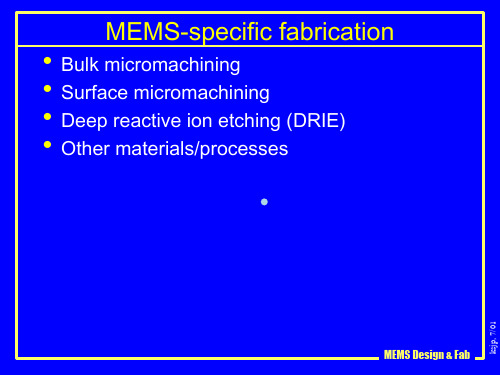
MEMS-specific fabrication
• Bulk micromachining • Surface micromachining • Deep reactive ion etching (DRIE) • Other materials/processes
MEMS Design & Fab
MEMS Design & Fab
ksjp, 7/01
Bulk micromachined cavities
• Anisotropic KOH etch (Upperleft) • Isotropic plasma etch (upper right) • Isotropic BrF3 etch with
• Isotropic silicon etchants
• HNA • HF, nitric, and acetic acids • Lots of neat features, tough to work with
• XeF2, BrF3 • gas phase, gentle • Xactix, STS selling research & production equipment
MEMS原理-01
• Closed-loop, microscale control of electrical, thermal, fluid, magnetic, optical, and mass flux
MEMS is a surface technology
Control phenomena on the microscale Cause large effects both on macroscale and microscale
Richard E. Smalley
……
Basic Introduction to MEMS
What are MEMS? – Definition
Scales of MEMS.– Some examples History …
Focus on MEMS
Classification of MEMS
What are MEMS ?
(3)
• High spatial resolution and high temporal bandwidth
Integrated solutions offer greater physical density Miniaturized components offer faster response
Size: 1 cm2 Power: 10 mW
Solar powered PicoRadio Node BWRC-BMI
10 grams 2cm x 2cm x 0.5cm ~ 1mW 100Kg’s $500
Comparison
Mass spectrograph (质谱仪)
Comparison
Solar Cell
《MEMS设计技术》课件

案例二:MEMS陀螺仪在导航系统中的应用
总结词
MEMS陀螺仪是导航系统中的关键传感 器,具有高精度、小型化和低成本等特 点。
VS
详细描述
MEMS陀螺仪采用微机械加工技术,将陀 螺仪的机械部分和电路部分集成在一个芯 片上,具有体积小、重量轻、成本低等优 点。它能够测量和保持方向信息,广泛应 用于航空、航天、军事等领域。在导航系 统中,MEMS陀螺仪可以提供高精度的角 度信息,用于计算航向、姿态和位置等参 数。
可靠性测试
进行全面的可靠性测试和评估,确保 MEMS器件的稳定性和可靠性。
06
MEMS设计案例分析
案例一:MEMS压力传感器在汽车中的应用
总结词
汽车压力传感器是MEMS技术的重要应用之一,具有高精度、可靠性和稳定性等特点。
详细描述
汽车压力传感器主要用于监测发动机进气歧管压力、燃油压力、气瓶压力等,以确保发动机正常工作 和提高燃油经济性。MEMS压力传感器采用微型机械加工技术,具有体积小、重量轻、功耗低等优点 ,能够实现高精度、快速响应和长期稳定性。
惯性传感器的设计需要综合考 虑材料、工艺和信号处理等因 素,以确保其性能和可靠性。
化学传感器设计
01
化学传感器是用于检测气体或 液体的化学成分的传感器,其 设计需要考虑选择性、灵敏度 、稳定性等因素。
02
常用的化学传感器类型包括电 化学式、光学式和热导式等, 其工作原理和结构各不相同。
03
化学传感器的设计需要综合考 虑材料、工艺和信号处理等因 素,以确保其性能和可靠性。
MEMS的发展历程与趋势
要点一
总结词
MEMS的发展经历了萌芽期、发展期和成熟期三个阶段, 未来将向更小尺寸、更高精度和智能化方向发展。
mems器件的书

mems器件的书以下是几本关于Mems器件的书籍:1. "Fundamentals of Microfabrication and Nanotechnology" by Marc J. Madou - 这本书提供了关于微加工和纳米技术的基本知识,包括MEMS器件的设计、加工和应用。
2. "Introduction to Microelectromechanical Systems Engineering" by Nadim Maluf and Kirt Williams - 这本书介绍了MEMS技术的基本原理和设计方法,并提供了一些实际的例子和应用。
3. "MEMS for Automotive and Aerospace Applications" by S. O. Reza Moheimani - 这本书重点介绍了MEMS技术在汽车和航空航天领域的应用,包括传感器、执行器等方面。
4. "MEMS: Design and Fabrication" by Mohamed Gad-el-Hak - 这本书提供了MEMS器件设计和制造的详细指南,包括材料选择、加工过程、工具和技术。
5. "MEMS Mechanical Sensors" by Scott D. Collins - 这本书专注于MEMS技术在机械传感器方面的应用,包括压力传感器、加速度计和惯性导航系统等。
6. "MEMS: Applications" edited by Vikas Choudhary - 这本书收集了关于MEMS技术在各个领域应用的文章,包括医疗器械、通信设备、环境监测等。
这些书籍可以帮助读者了解MEMS器件的原理、设计和应用,对于学习和研究MEMS技术非常有帮助。
《微电子与集成电路设计导论》第六章 新型微电子技术
纳电子器件——Memristor忆阻器 ➢ 全称记忆电阻(Memristor),是表示磁通与电荷关系的电路器件。
特点
➢ 电阻取决于多少电荷经过了器件。 ➢ 若电荷以一个方向流过,电阻会增加;
如果让电荷以反向流动,电阻就会减小。 ➢ 具有记忆能力,断电后电阻值保持不变。
纳电子器件——石墨烯
➢ 它是已知材料中最薄的一种,且牢固坚硬; ➢ 优良的导电特性:它在室温下传递电子的速度比已知导体都快。
优势
➢ 碳纳米管FET沟道为一维结构,载流子 迁移率大大提高。
➢ 碳纳米管FET参与碳纳米管导电的是表 面。
➢ 碳纳米管FET通过选择源漏材料,可完 全消除源漏结势垒
图6.4.2 CNT-FET典型结构示意图
纳电子器件——有机分子场效应晶体管
该技术利用了分子之间可自由组合的化学特性,晶体管电极之间的距离仅为1纳米到2 个纳米,是目前世界最小的晶体管。同时具有制造简单,造价低廉的优点。
2006年3月, 佐治亚理工学院 (Georgia Institute of Technology) 的研究 员宣布,成功地制造了石墨烯平面场效应 晶体管并观测到了量子干涉效应。并基于 此研究出根据石墨烯为基础的电路。
6.4.2 纳电子材料
纳米材料一诞生,即以其异乎寻常的特性引起了材料界的广泛关注。这 是因为纳米材料具有与传统材料明显不同的一些特征。
人类社会是在不断征服自然和不断攀登科技顶 峰而前进的,纳米技术也是如此。
现在世纪纳米技术和纳米材料,正向新材料、 微电子、计算机、医学、航天、航空、环境、 能源、生物技术和农业等诸多领域渗透。
纳米打假
纳米技术并非高不可攀,但也决非人人都能“纳”一把, 因此,我们要提前做好纳米技术的打假工作,建立一套十分 严格的评审和考核制度,为纳米技术的发展创造良好的空间, 防止样样都要“纳”一把现象的发生,尽量避免恶意炒作 “伪纳米”,不能等到造成极其严重的恶果后,再去打与堵。
introductiontomicro-fabricationtechnology
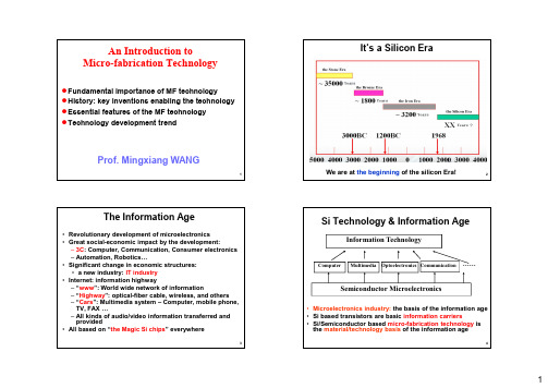
1An Introduction toMicro-fabrication Technology●Fundamental importance of MF technology●History: key inventions enabling the technology ●Essential features of the MF technology ●Technology development trendProf. Mingxiang WANG2It’s a Silicon EraWe are at the beginning of the silicon Era!The Information Age•Revolutionary development of microelectronics •Great social-economic impact by the development:–3C : Computer, Communication, Consumer electronics –Automation, Robotics…•Significant change in economic structures:• a new industry: IT industry •Internet: information highway–“www ”: World wide network of information–“Highway ”: optical-fiber cable, wireless, and others –“Cars ”: Multimedia system –Computer, mobile phone, TV, FAX …–All kinds of audio/video information transferred and provided•All based on “the Magic Si chips ” everywhere3Si Technology & Information Age•Microelectronics industry: the basis of the information age •Si based transistors are basic information carriers•Si/Semiconductor based micro-fabrication technology is the material/technology basis of the information ageInformation TechnologyComputer Multimedia CommunicationOptoelectronics ……Semiconductor Microelectronics4Historical milestones:key inventions enablingthe IC micro-fabrication technology •1st transistor 1947•1st junction transistor 1949•1st integrated circuit 1958•1st monolithic integrated circuit 1959•Invention of the planar process 1960•1st silicon MOSFET 19605Invention of Transistor•1947.12.23: Invention of pointcontact transistor by Bardeen &Brattain–1st paper on Transistor: “Thetransistor, a semiconductortriode”, Phys. Rev. 74, 230,1948–By Webster’s:Transistor = transfer + resistortransferring electrical signalacross a resistor6How does the 1st transistor works? John Bardeen, Nobel lecture, Dec.11, 1956 Semiconductor research leading to the pointcontact transistor7First transistor & its inventors 1947, John Bardeen, Walter Brattain & William Shockley,Bell lab (1956 Nobel Prize winner in Physics)8 Shockley developed basic theory of transistor (1948-1952)First PN Junction TransistorWilliam Shockley Gordon Teal Morgan SparksGordon Teal and Morgan Sparks made the first junction transistor in 1949,the construction of which eliminated many of the reliability problems of the point contact transistor.99/21/2013•1958.9.12 1st IC---“Solid Circuit” by J. Kilby of TI –Flip-flop phase shift oscillator–On Ge substrate–Mesa structure with 1 BJT, 3R, and 1C–Etching by black wax protection–Wire bond interconnect2000 Nobel Prize in Physics on Integrated Circuits (shared with Afilov and Kroemer )First Integrated Circuit101st monolithic IC by R.N. Noyce 1959 (Fairchild) –First micro-chip –On Si substrate–Flip-flop circuit with 6devices by Al interconnect –Based on Si BJT which is first made in 1954 (TI)First monolithic IC11Invention of Planar Process•1958-1960 b asic IC process developed: oxidation (Atalla; bell Lab), pn junction isolation (K. Levovec), Al film evaporation…•1960Si planar process inventedInventor :Jean Hoerni --Fairchild1213First MOS Transistors1st MOSFET Bell lab 1960•1959-63: MOS devices–1959: MOS capacitor (J. Moll; Stanford)–1960: Kahng & Atalla(Bell lab), structure same as modern MOSFETs –1960-63: research on Si surface & MOS devices (Sah, Deal, Grove…)–1963: concept of CMOS (Wanlass, Sah; Fairchild)14Modern Micro-Processor Unit1st CPU, 2300T Intel 4004, 1971, 8umIntel dual-core MPU, 410MT ,Nov. 2007, 45nm15Flowchart of IC fabrication16Essential Featuresof Micro-fabrication Technology●Extremely capital intensiveHeavy capital Investment for clean rooms & Fab equipments ●Batch Process:>100 Billion Transistors per wafer ●Outstanding Manufacturability : Yield>95% per lot●Extremely cheap productsContinuously lower price per function ●Technology widely extendable17Capital intensive●Heavy capital investment for -clean rooms -fab equipments-materials used in a fab: rigorous requirements ●Estimated cost for a fab-Intel’s Fab22 in Arizona (8-inch, 0.13μm, copper based) opened in October 2001 cost 2 billion USD (cost of 2 Tsing Ma Bridges!)-Cost for a new 12-inch 45-65nm generation fab cost about 10 billion USD->70% cost used for equipments●NOT affordable by most countries!18300mm Global Fab LandscapeUnited States IBM Bldg 323Infineon Richmond Intel D1C Intel D1D Intel F11x Intel F12C Micron MTC TI DMOS 6TI DMOS 7JapanElpida Fab 1Elpida Fab 2Renesas/ Trecenti Toshiba OitaSony Kumamoto Sony Fab 2 Nagasaki Toshiba Yokkaichi City NEC Elec Yamagata TaiwanPowerchip Fab 1ProMOS Fab 2TSMC Fab 12A & B UMC Fab 12AInotera (Nanya + Infineon)Powerchip Fab 1Powerchip Fab 2TSMC Fab 14SingaporeUMC SingaporeEuropeAMD Fab 36Infineon SC300Intel Fab 24Crolles2 (TD)(STM, Philips, Moto)STM CataniaKoreaSamsung Line 12Samsung Line 13Samsung Line 14Sources: Silicon Strategies, EE Times, Nikkei Microelectronics, Industry MeetingsChinaSMIC Fab 419Toshiba Oita Works 300 mm Fab TSMC300 mm Super clean room in Tsukuba,SeleteIntel fabFab20NikonArF Scanner l = 193nm 2004Contact mask aligner 1970’sMainstream photo-lithography21Single Crystal Silicon300mm and 400mm Silicon Ingots w/o a single defects22When do we start planning for nextwafer size transition?9 yrs + 2 yrs delay*9 yrs + 6 yrs delay? 9 yrs + ?yrs delay675mm/2025?450mm/2015?300mm/2001200mm/1990 (125/150mm -1981)We are hereWhen does this happen?23Batch process●Requirement of cost recoveryhave to produce >10,000 wafers per month to recover the cost of 12-inch fab investment●Batch process->100 Billion transistors per wafer fabricated in parallel-sometimes ~20 wafers per lot processed in parallel -extremely productive●The essential feature of the planar process ●Ensure that fabricated products are cheap24Intel 300 mm75 mm, 100 mm, 50 mmWafers25Outstanding Manufacturability●Yield >95%per lot to earn money -evaluated by chip function●About 108(0.1 billion) transistors per ULSI chip, which would FAIL if only one transistor, one metal line, one contact or one other component fails!●What’s the yield at transistor/component level to achieve 95% yield at chip level?●Reliability: lifetime >10yrs●What’s other technologies could have such ability? -yield, batch process, micro/nano-fabrication, …26Modern MPU Chip1st CPU, 2300T Intel 4004, 1971, 8um Intel dual-core MPU, 410MT ,Nov. 2007, 45nm27Inside the chips28Electron Micrograph on MOS interface29Continuously cheaper products●Moore’s law means exponential decay of the price per function●What’s the price of a “car” if Moore’s law also holds?●The continuous price reduction is a tremendous competitiveness over traditional technology●Cheap product means the tremendous impact of the new technology is affordable to everyone!●A simple and strong reason why Silicon Era becomes the reality30Technology extendable●It’s more than an IC technology!●It’s more than just 3Cs,the micro-fabrication technology is widelyextendable to address almost all issues in our life ●Solar cells, photo-voltaic industry, energy harvest ●LED lightings●Flat panel displays, Thin film electronics ●MEMS devices: Sensors and Actuators ●Bio-chips, Health care…●It’s another strong reason why we are in Silicon Era!31Other applications of micro-fabrication(Source: University of Florida)32MEMS devices: an extension of Siplanar processEtched profiles of MEMS structures33Technology Development Trends ●Moore’s Law:would continues for another 30yrs ●More than Moore (MtM):●Micro-Systems: SoC, SiPMoore’s Law•Double the number of transistor every 18-24 months •Exponential growth ofsemiconductor technology & industry (A common law at early stage for a new industry under rapid development)•Govern the trend since 1960 and would continue in the next 20-30 yrs •An economics law of technology and market expansionFirst proposed in 1965by Gordon Moore ,co-founder of Intel3435New Generations under Moore’s Law●A new generationper 18-24 months ●X0.7 Min. feature size scaling ●X2 increase in transistor density ●X1.5 faster device switching speed ●Reduced chip power●Reduced chip cost●Increased functionality3619001950196019702000Vacuum Tube Transistor IC LSI VLSI 10 cm cm mm 10 m m 100 nm In 100 yrs, the feature size reduced by 106times Technology driver: BJT —CMOS —DRAM/CPU —Flash —Communication10-1m10-2m10-3m10-5m10-7mDownsizing of the components has been the driving force for circuit evolution37Transistor Scaling38Device feature sizeIntel 90nm Tech. Node Transistor Smallest species: VirusIn another 30yrs, device feature size wouldapproach molecular size <1nm (could be a limit), before which Moore’s law still continues.The Paradox of Moore’s Law●As transistors grow smaller, opportunities grow largerAs the basic element of information,and the basis ofthe information society ,IC &related micro-fabrication technology have been deeply involving into all hi-tech fields.3940More than Moore’s Law●More than Moore (MtM) Law:●System level Integration: SoC, SiP , it is the system that matters !●Micro-fabrication technology follows the trend of SoC and SiP, under Moore’s law as well as under More than Morre’s Law .9/21/2013414344。
MEMS 教程 Lecture16
Final Exam details
50% multiple choice. 50% free response. All multiple choice material come from previous quizzes Questions will be worded slightly differently than on quizzes Questions will focus on understanding concepts and applications, not rote memorization Exception: You must know certain “famous” MEMS devices by name (e.g. Texas Instruments DMD, Analog Devices ADXL 50). Free response questions will require you to sketch drawings Know Know Know Know how basic devices look how basic devices work basic sizes and materials how fabrication processes work
Introduction to MEMS Final Review A review of some of the many issues discussed in this class
Introduction to MEMS lecture #16 FINAL LECTURE Mark Bachman, UCI, Fall 2004
16
Diffuser valve devices
You should know: Basic design, materials, operation, application, fabrication
mems设计

mems设计MEMS(Micro-Electro-Mechanical Systems)是微电子力学系统的简称,是一种将微纳技术与电子技术相结合的技术领域。
它主要由微电子部分和微机械部分组成,具有微型、高效、低功耗等特点。
MEMS的设计是将微机械结构与电子元件集成在一起,以实现检测、控制、测量等功能。
MEMS设计的目的是通过优化设计、材料选择和工艺流程,使得设备在小尺寸下具有高精度、高灵敏度、高可靠性和低功耗等特性。
在MEMS设计中,需要考虑到以下几个关键因素。
第一,设计需要满足设备的功能要求。
根据具体应用需求,设计师需要确定MEMS设备所需的传感、控制和测量功能。
例如,MEMS加速度计的设计需要考虑到灵敏度、频率响应、稳定性等因素;MEMS压力传感器的设计需要考虑到量程、线性度、温度漂移等因素。
设计师需要充分了解应用要求,并将其转化为MEMS器件的设计指标。
第二,设计需要考虑到制造工艺的可行性。
MEMS器件在制造过程中需要采用高精度的加工方法,例如光刻、薄膜沉积、离子刻蚀等。
设计师需要了解这些工艺的限制和能力,合理选择器件的材料和结构。
在设计过程中,需要避免过于复杂的结构、过高的结构比例和难以加工的特殊结构。
第三,设计需要考虑到器件的尺寸和功耗。
MEMS器件的尺寸通常在微米到毫米级,所以设计师需要充分利用微纳尺度的特性来优化设备结构和性能。
另外,由于许多MEMS器件是面向便携和无线应用,因此功耗的控制也是设计过程中的一个重要考虑因素。
设计师需要通过减小能耗、优化电源管理和控制技术等手段来实现低功耗。
第四,设计需要考虑到器件的可靠性和环境适应性。
MEMS器件常常面临复杂的工作环境和较大的物理力加载。
设计师需要通过材料选择、结构优化和应力分析等手段,确保器件在各种工作条件下都能保持稳定可靠的性能。
另外,由于MEMS器件对湿度、温度和化学环境等比较敏感,设计师还需要考虑到环境适应性问题。
总体来说,MEMS设计是一个综合性的任务,需要设计师具备微纳技术、电子技术和机械工程等多个领域的知识。
中科院 微电子机械系统设计(MEMS)课件

10 nm < L < 1 µm Nano electromechanical systems … NEMS
Batch Fabrication Technology
Planar integrated circuit technology 1958 1. Thin-film deposition and etching 2. Modification of the top few µm of the substrate 3. Lateral dimensions defined by photolithography, a process derived from offset printing Result: CMOS integrated circuits became the ultimate “enabling technology” by circa 1980 Moore’s Law Density (and performance, broadly defined) of digital integrated circuits increases by a factor of two every year.
Lecture Outline
Today’s Lecture
What is MEMS Historical tour of MEMS MEMS and nanotechnology
MEMS Defined
Micro ElectroMechanical Systems
What is MEMS
MEMS involve both electronic and non-electronic elements
Dimensional Ranges
国 外 大 学 部 分 现 用 教 材 及 教 学 参 考 书
Vibration simulation using MATLAB and ANSYS/振动问题的MATLAB和ANSYS仿真
Chapman & Hall/CRC/c2001
本书可以作为机械工程学科以及控制学科高年级本科生、研究生振动课程的参考书。
TH113.2 FC53k
John Wiley & Sons, Inc. /c2001.
本书可作为工程科学各学科研究生第一学期的课程用教材。
O152.5 FT58
Abstract root subgroups and simple groups of Lie-type/抽象根子群与李型单群
Birkhser Verlag/c2001
TN305.2 FE52
Silicon micromachining/硅微机械加工
Cambridge University Press/c1998
本书结合了理论知识和实验知识,适合电子工程、材料科学等专业,尤其是与微机电系统(MEMS)相关专业的研究生学习使用。
TN4 FH871
MEMS & microsystems :|bdesign and manufacture/微机电系统和微系统:设计和加工
Academic Publishers/c2001.
目前是许多著名大学MEMS课程的首选教材或者参考资料,特别适合作为研究生以及高年级本科生学习MEMS的教材使用。
TN405.7 FL66
Principles of lithography/光刻原理
SPIE Press/c2001.
本书可以作为微光刻技术领域初学者的入门教材。
Artech House/c2000
研究生中英文课程名称对照表

马克思主义发展史 马克思主义发展史研究 马克思主义经典著作选读 马克思主义经济学专题研究 马克思主义前沿问题研究 马克思主义与当代世界社会主义 马克思主义与社会科学方法论 马克思主义与中国文化 马克思主义原理研究 马克思主义哲学原著 马克思主义哲学原著选读 马克思主义哲学专题研究 马克思主义中国化前沿问题研究 码分多址原理 码分多址原理与应用 漫画创意与艺术欣赏 漫画创意与艺术欣赏(人文艺术类) 毛泽东思想研究 媒介经营与管理 媒介批评 媒体广告学 媒体艺术研究 美国南方文学 美国网络法 密码理论新进展 面向对象技术与C++编程 面向对象技术与C++编程(三班) 面向对象技术与C++编程(四班) 面向对象系统的分析与设计 民法学分论 民法学总论 民商法学总论 民商事争议解决机制 民事诉讼法 模糊控制 模糊数学 模式识别导论 纳米材料学 纳米材料学导论 纳米光电子学 纳米光学基础 诺贝尔经济学奖得主思想评述 排队论与随机服务系统 品牌形象与战略研究 普通英语语言学 企业会计报表案例分析 企业信息化工程实训 企业咨询与诊断 前沿课题讲座 嵌入式技术实验 嵌入式通信系统设计与开发 嵌入式系统 嵌入式系统工程实训 嵌入式系统实验
Switching and routing Technical Research and Professional Skills Telecommunication Competition and Regulation Theory of Information & Channel Trend of Telecommunication Unified Theory of Artificial Intelligence UNIX环境高级编程 Verilog HDL 设计及EDA技术基础 Verilog HDL设计及EDA技术基础 VHDL语言与ASIC设计 VLSI系统设计与CAD方法 VLSI原理与设计 VLSI中的HDL设计 Walsh函数 Walsh函数与Hadamard矩阵 Web搜索 Web应用开发技术 Windows应用软件界面设计 Windows应用软件设计与实践 XML与 Web Service X-射线分析技术 半导体材料生长与检测 半导体材料物理学 半导体光电子学导论 半导体光电子学科学问题及关键工艺 半导体量子器件物理 半定规划及其应用 比较行政体制专题研究 编码理论 标记语言 标准化概论 标准化概述 表面微观探测技术 并行计算方法与应用 并行计算理论与方法 博士英语 博士英语(听说) 博士英语(写译) 博弈论 不确定性人工智能 材料的力学性能 财税理论与实践 产品设计研究 产权理论专题 产业经济学前沿问题研究 产业组织理论 超宽带扩频通信 超宽带无线通信 程序设计方法学 传播学理论专题研究 传播学研究方法 传感器与物联网 传媒经济学 传送网技术
- 1、下载文档前请自行甄别文档内容的完整性,平台不提供额外的编辑、内容补充、找答案等附加服务。
- 2、"仅部分预览"的文档,不可在线预览部分如存在完整性等问题,可反馈申请退款(可完整预览的文档不适用该条件!)。
- 3、如文档侵犯您的权益,请联系客服反馈,我们会尽快为您处理(人工客服工作时间:9:00-18:30)。
MEMS Design & Fab
ksjp, 7/01
References • Conferences
• Sensors and Actuators Workshop (Hilton Head), even years, Hilton Head Island, SC. N. America only
• MOEMS, 97 Japan, 98 U.S. (LEOS), 99 Germany • SPIE, annual, San Jose, CA. (formerly Austin, TX) • LEOS, OSA, CLEO • ASME •…
MEMS Design & Fab
ksjp, 7/01
Introduction to MEMS Design and Fabrication
Kristofer S.J. Pister Berkeley Sensor and Actuator Center
UC Berkeley
MEMS Design & Fab
ksjp, 7/01
A brief history of MEMS
• Kovacs, Micromachined Transducers Sourcebook, McGrawHill
• Madou, Fundamentals of Microfabrication, CRC • Maluf, An Introduction to Microelectromechanical Systems
• 1750s first electrostatic motors (Benjamin Franklin, Andrew Gordon) • 1824 Silicon discovered (Berzelius) • 1927 Field effect transistor patented (Lilienfield) • 1947 invention of the transistor (made from germanium) • 1954 Smith, C.S., "Piezoresistive effect in Germanium and Silicon, Physical Review, 94.1,
References
• Periodicals
• IEEE/ASME, JMEMS • Sensors and Actuators A/B • J. Micromechanics and Microengineering • Sensors and Materials
MEMS Design & Fab
ksjp, 7/01
References • Books
• Elwenspoek and Jansen, Silicon Micromachining, Cambridge
• Keller, Microfabricated High Aspect Precision Instruments
April 1954.
• 1958 silicon strain gauges commercially available • 1961 first silicon pressure sensor demonstrated (Kulite) • 1967 Invention of surface micromachining (Nathanson, Resonant Gate Transistor) • 1970 first silicon accelerometer demonstrated (Kulite) • 1977 first capacitive pressure sensor (Stanford) • 1980 Petersen, K.E., "Silicon Torsional Scanning Mirror", IBM J. R&D, v24, p631, 1980. • 1982 disposable blood pressure transducer (Foxboro/ICT, Honeywell, $40) • 1982 active on-chip signal conditioning • 1984? First polysilicon MEMS device (Howe, Muller ) • 1988 Rotary electrostatic side drive motors (Fan, Tai, Muller) • 1989 Lateral comb drive (Tang, Nguyen, Howe) • 1991 polysilicon hinge (Pister, Judy, Burgett, Fearing) • 1992 Grating light modulator (Solgaard, Sandejas, Bloom) • 1992 MCNC starts MUMPS • 1993? first surface micromachined accelerometer sold (Analog Devices, ADXL50) • 1994 XeF2 used for MEMS (OK, so this one isn’t as important as the others)
• IEEE MEMS workshop, annual, 00 Japan, 01 Europe, 02 U.S.
• Intl. Conf. Solid State Sensors and Actuators (Transducers), odd years, 99 Japan, 01 Europe, 03 U.S.