HD44780(KS0066)中文数据手册
HD44780-LCD使用说明书-无底字

八 责任范围及维修
在您购买液晶显示模块时 精电蓬远将会为您做显示模块的检测 确保您所买的显
示模块为完好的器件 在您使用过程中因不小心将显示模块损坏 您可送至精电蓬远维
修部修理 液晶模块如果出现屏被损坏的问题 比如玻璃面破损 玻璃屏角碎裂等等
将无法进行修理 您的液晶模块只能报废
公司产品质量都是通过国际质量认证及时间的考验的 请用户放心使用 如果在使
符号
VIH VIL VOH VOL IDD
条件
IOH = 0.2 mA IOL = 1.2 mA
S
S — STN 超扭曲相列型 空缺 — TN 扭曲相列型
40466 点阵数
HT
工作温度
HV
驱动电压类型
G
STN模式: G — 黄/绿模式 S — 银色模式 B — 蓝模式 反显
F — 黑/白模式 带有补偿膜的FSTN型 D — 黑/白模式 双STN型
LED04 背光类型 LED01 LED02 LED03 LED04 EL CCFL
-2-
点阵字符型液晶显示模块使用手册
四 装配操作时的注意事项 1. 模块是经过精心设计组装而成的 请勿随意自行加工 修整 2. 金属框爪不得随意扭动 拆卸 3. 不要随意修改加工PCB板外形 装配孔 线路极其部件 4. 不得修改导电胶条 5. 不得修改任何内部支架 6. 不要碰 摔 折曲 扭动模块
V*
8+.
&$VQ&$
8+* 8+.
8CNKFFCVC V E[E'
8+* 8+.
9TKV G1R GT CVKQP
项目
使能周期 使能脉冲宽度 使能升 降时间 地址建立时间 地址保持时间 数据建立时间 数据保持时间
HD44780中文数据手册
运行时间(250Khz): 40 µs 功能:设置显示、光标及闪烁开关。 其中:D表示显示开关:D = 1为开,D = 0为关;
C表示光标开关:C = 1为开,C = 0为关; B表示闪烁开关:B = 1为开,B = 0为关。 5、光标、画面位移
运行时间(250Khz): 40 µs 功能:光标、画面移动,不影响DDRAM。 其中:S/C = 1: 画面平移一个字符位;
Tas Tah Tdsw Th
最小值 1000 450
140 10 195 10
最大值 25 -
单位 ns ns ns ns ns ns ns
项目
符号
最小值
பைடு நூலகம்最大值
单位
使能周期
TcycE
1000
-
ns
使能脉冲宽度
Pweh
450
-
ns
使能升降时间 Ter,Tef
-
25
ns
地址建立时间
Tas
140
-
ns
地址保持时间
3. 模块使用时,接入逻辑电源和驱动电源的顺序,应是先逻辑电源,后驱动电源,断电时应 先驱动电源,后逻辑电源,这样做有助于保持屏的良好显示效果和避免在上电、断电时的电压冲击 损坏。所以推荐使用带控制的DC-DC电源做为模块的驱动电源。
HD44780详解
PIC单片机与基于HD44780液晶显示模块接口的设计作者:林曙光黄超昔武凌摘要:介绍了基于HD44780液晶显示模块的基本特性及其与PIC单片机的接口,并给出了常用的显示子程序。
关键词:单片机;液晶显示;接口;子程序基于HD44780的字符型液晶显示模块是一种常用的液晶显示器件,主控制驱动电路为HD44780(HITACHI),其他一些公司的电路与之全兼容,如NOVATEK 的NT3881,SAMSUNG公司的KS0066,SUNPLUS公司的SPLC78A01。
由其控制的液晶显示器可以提供若干个5×7或5×10点阵块组成的显示字符群,每个点阵块为一个字符位,字符间距和行距都为一个点的宽度,具有64 B的自定义字符RA M,可自定义8个5×8点阵字符或4个5×11点阵字符。
可以提供8×1~40×4(字符数×行数)各种显示屏规格,广泛应用于智能仪表、通讯、办公自动化及军工等领域。
1液晶显示模块的特点1.1 引脚功能表1是一种基于HD44780的液晶显示模块的引脚功能。
有些显示模块有2个使能端,这种器件可以提供多达4行的显示屏,一个使能端可以控制2行。
当RS和R/W都为低电平时可以写入指令或显示的地址;当RS为高电平、R/W为低电平时,可以写入要显示的数据;当RS为低电平、R/W 为高电平时,可以读出忙信号和地址计数器(CGRAM或DDRAM的值)。
当使能端E由高电平变为低电平时,液晶模块执行写操作(写入命令或要显示的数据、地址);D0~D7为双向数据线。
真值表如表2所示。
1.2 指令集(1)清屏功能:清显示屏,光标回到00H处。
(2)归位功能:光标复位回到00H处。
(3)输入模式设置功能:设置光标和显示模式。
其中:I/D=1时光标向右移,I/D=0时光标向左移;S=1屏幕上的文字可以移动,S=0屏幕上的文字不可以移动。
(4)显示开关控制功能:设置显示、光标及闪烁开、关。
HD44780使用手册
3
Table of Contents
1 FUNCTION AND STRUCTURE.........................................................................................................6 1.1 GENERAL .............................................................................................................................................6 1.2 CHARACTERISTICS................................................................................................................................6 1.3 HANDLING PRECAUTIONS .....................................................................................................................7 1.4 LIST OF DMC SERIES ...........................................................................................................................8 1.5 PIN ASSIGNMENTS .................................
LCD1602数据手册LCD16...

LCD1602数据手册1602采用标准的16脚接口,其中:第1脚:VSS为地电源第2脚:VDD接5V正电源第3脚:V0为液晶显示器对比度调整端,接正电源时对比度最弱,接地电源时对比度最高,对比度过高时会产生“鬼影”,使用时可以通过一个10K的电位器调整对比度第4脚:RS为寄存器选择,高电平时选择数据寄存器、低电平时选择指令寄存器。
第5脚:RW为读写信号线,高电平时进行读操作,低电平时进行写操作。
当RS和RW共同为低电平时可以写入指令或者显示地址,当RS为低电平RW为高电平时可以读忙信号,当RS为高电平RW为低电平时可以写入数据。
第6脚:E端为使能端,当E端由高电平跳变成低电平时,液晶模块执行命令。
第7~14脚:D0~D7为8位双向数据线。
第15~16脚:空脚1602液晶模块内部的字符发生存储器(CGROM)已经存储了160个不同的点阵字符图形,如表1所示,这些字符有:阿拉伯数字、英文字母的大小写、常用的符号、和日文假名等,每一个字符都有一个固定的代码,比如大写的英文字母“A”的代码是01000001B(41H),显示时模块把地址41H中的点阵字符图形显示出来,我们就能看到字母“A”1602液晶模块内部的控制器共有11条控制指令,如表2所示,它的读写操作、屏幕和光标的操作都是通过指令编程来实现的。
(说明:1为高电平、0为低电平)指令1:清显示,指令码01H,光标复位到地址00H位置指令2:光标复位,光标返回到地址00H指令3:光标和显示模式设置 I/D:光标移动方向,高电平右移,低电平左移 S:屏幕上所有文字是否左移或者右移。
高电平表示有效,低电平则无效指令4:显示开关控制。
D:控制整体显示的开与关,高电平表示开显示,低电平表示关显示 C:控制光标的开与关,高电平表示有光标,低电平表示无光标 B:控制光标是否闪烁,高电平闪烁,低电平不闪烁指令5:光标或显示移位 S/C:高电平时移动显示的文字,低电平时移动光标指令6:功能设置命令 DL:高电平时为4位总线,低电平时为8位总线 N:低电平时为单行显示,高电平时双行显示 F: 低电平时显示5x7的点阵字符,高电平时显示5x10的点阵字符指令7:字符发生器RAM地址设置指令8:DDRAM地址设置指令9:读忙信号和光标地址 BF:为忙标志位,高电平表示忙,此时模块不能接收命令或者数据,如果为低电平表示不忙。
lcd段码屏驱动原理

lcd段码屏驱动原理
LCD段码屏是一种常见的数字显示设备,它的驱动原理主要涉及到显示控制芯片和显示模块两个方面。
1. 显示控制芯片
LCD段码屏的显示控制芯片通常采用CMOS技术制造,它可以通过内部的控制逻辑和存储器,控制LCD每一段的电压信号,从而实现数字图像的显示。
常见的LCD控制芯片有HD44780、KS0108、KS0066等,其中HD44780是一种具有广泛应用的标准控制芯片。
2. 显示模块
LCD段码屏的显示模块由多个LCD段组成,每个LCD段由数根独立的导电柱和两根金属屏蔽板组成,通过在导电柱和金属屏蔽板之间加电压差,实现液晶分子的定向排列,进而改变透射光的相位差,实现数字图像的显示。
在不同的电压条件下,液晶分子的定向状态也不同,对应不同的显示状态。
因此,通过控制每一段的电压信号,就可以实现数字图像的显示。
总结:
LCD段码屏的驱动原理主要包括显示控制芯片和显示模块两个方面。
通过控制每一段的电压信号,就可以实现数字图像的显示。
海量的应用场景,让段码屏成为了数字显示的中坚力量。
hd44780组成和使用方法
hd44780组成和使用方法宝子!今天咱们来唠唠HD44780这个超有趣的东西。
先说说它的组成吧。
HD44780呀,它内部结构就像是一个小小的智能世界。
它有控制器部分,这个就像是大脑,指挥着整个显示的运作呢。
还有显示数据存储器,就像是个小仓库,把要显示的字符或者图形的数据都妥妥地存起来。
再加上字符发生器,这个可厉害啦,能把那些存好的数据变成咱们能看到的字符形状。
那这个HD44780咋使用呢?要是你想让它显示点东西,就像让它给你说句温馨的小话。
你得先把它和你的电路连接好,就像是给它搭好舞台一样。
一般来说,有数据总线要连好,这就像是在它和你的控制设备之间建了个信息高速公路,数据就在这上面跑来跑去的。
然后呢,你得给它发送指令。
这指令就像是你对它下的小命令。
比如说你想让它显示个“你好”,你得先告诉它要在哪个位置显示,是第一行呢还是第二行。
这就好比你告诉一个小助手,把这个东西放在哪个架子上一样。
在发送数据的时候呀,你得按照它的规矩来。
它就像个有点小脾气的小伙伴,数据的格式、顺序都得对。
要是弄错了,它可能就会给你显示个乱码,就像小朋友调皮地做个鬼脸,告诉你“你错啦”。
还有哦,它的电源供应也很重要。
就像人要吃饭一样,它得有合适的电压来维持它的活力。
如果电压不稳,它可能就会表现得怪怪的,就像人饿了没力气干活一样。
你要是想调整显示的样式,比如让字变大一点或者变个颜色(这得看它外接的显示模块有没有这个功能啦),那也得通过发送特定的指令来实现。
这就像是给它打扮一样,你得告诉它今天要穿什么样的衣服,是漂亮的裙子(某种显示样式)还是帅气的裤子(另一种显示样式)。
总的来说呢,HD44780虽然看起来有点复杂,但只要你耐心地去了解它的小脾气,按照它的规则来,就能让它乖乖地为你显示出各种有趣的东西啦。
就像和一个新认识的朋友慢慢磨合,最后成为超棒的搭档一样。
Matrix Multimedia LCD Display说明书
LCD Display datasheetContents1.About this document2.General information3.Board Layout4.Getting Starteders GuideAppendix1Circuit Diagram1 About this documentThis document concerns the Matrix LCD Display code EB-005-00-1.Trademarks and CopyrightPIC, PICmicro are registered trademarks of Arizona Microchip Inc.E-blocks is a trademark of Matrix Multimedia Limited.EB-005-00-1 and associated software and documentation are Copyright ©2004 Matrix Multimedia Limited. Other sources of informationThere are various other documents and sources that you may find useful:Getting started with E-Blocks.pdfThis describes the E-blocks system and how it can be used to develop complete systems for learning electronics and for PICmicro programming.PPP Help fileThis describes the PPP software and its functionality. PPP software is used for transferring hex code to a PICmicro microcontroller.DisclaimerThe information in this document is correct at the time of going to press. Matrix Multimedia reserves the right to change specifications from time to time.Technical supportIf you have any problems operating this product then please refer to the troubleshooting section of this document first. You will find the latest software updates, FAQs and other information on our web site: . If you still have problems please email us at:***************************.uk.Whenemailingpleasestatetheoperatingsystem,theversionofPPPyou are using.2 General informationDescriptionThis is an LCD Display designed for E-blocks. It is a 16 character, 2-line alphanumeric LCD display connected to a single 9-way D-type connector. This allows the device to be connected to most E-Block I/O ports.The LCD display requires data in a serial format, which is detailed in the user guide below. The display also requires a 5V power supply. Please take care not to exceed 5V, as this will cause damage to the device. The 5V is best generated from the E-blocks Multipogrammer or a 5V fixed regulated power supply.The potentiometer RV1 is a contrast control that should be used to adjust the contrast of the display for the environment it is being used in.Features•E-blocks compatible•Low cost•Compatible with most I/O ports in the E-Block range (requires 5 I/O lines via 9 way D-type connector)•Ease to develop programming code using Flowcode icons.3 LCD Board Layout1)9 Way D-type Plug2)16 character, 2-line alphanumeric LCD display3)9 Screw terminal4)Contrast Control4 Getting StartedAs can be seen the circuit diagram (Appendix 1) consists of a simple LCD circuit. To test this board you will need to apply 5V to the LCD Board via the screw terminal and then set the appropriate bits using the 9-Way D-type connector. The details off the LCD configuration are stated in the Chapter 4 Users’ guide. Testing the LED Board – LCD.hexThe following instructions explain the steps to test and use your LCD Board. The instructions assume that PPP is installed and functional. It also assumes that you are confident in sending a program to the PIC via the multiprogrammer.The LCD.hex program will place a counter on to the LCD Board1)Ensure power is supplied to all the necessary boards.2)Insert the LCD board into Port B of the Multiprogrammer3)Ensure that the Multiprogrammer is in correct configuration-Fast mode (SW1 towards the centre of the board)-Ensure that a 19.6608MHz crystal is inserted in the Multiprogrammer boardSW2 is not used when in Xtal mode so it doesn’t matter it’s position4)Program the a PIC16F88 with the test program LCD.hex5)Press the reset button on the Multiprogrammer.6)Adjust contrast accordingly.This should satisfy that the LCD Board is fully functional!4 Users’ guideThe LCD is a 16 character x 2 lines module. Internally it is 40 characters x 2 lines. Line 1 ranges from H’00’ to H’27’ and Line 2 ranges from H’40’ to H’67’.The LCD Module uses a Samsung KS0066U controller, which is similar to the Hitachi HD44780 controller. The PICmicro board uses pins 1 - 6 on the 9-way D-type connector to program the LCD, as shown in the circuit diagram below. When the LCD board is turned on, data can only be sent to it after 30ms, this is the time taken for the LCD to initialize [as it clears all the RAM and sets up the Entry Mode].LCD Block DiagramTo 9-way D-type ConnectorTo send a command to the LCD, data must be sent in two steps, the MSB followed by the LSB [byte is data on pins 1 - 4]. As each byte is sent to the LCD, B5 must be go high then low, for the LCD to acknowledge the byte. After the second byte has been acknowledged the LCD executes the command. The PICmicro board must wait for at least the length of the execution time for that command, before the next command can be sent. A timing diagram of this process is shown below.LSB MSB LSBMSB Pin 6Pins 1- 4LCD BusyTimingDiagramThe first command to be sent to the LCD must be ‘Function Set’ [to setup the LCD], this is usually followed by ‘Display Control’ and then ‘Clear Display’. According to ‘Entry Mode Set’ after each character is sent to the LCD, the position of the cursor changes [by default it is incremented].Bit Name01I/D SH D C B S/C R/L Decrement cursor position Increment cursor positionCursor blink onCursor blink offMove cursor Shift displayShift left Shift rightCursor onCursor offDisplay onDisplay offDisplay shiftNo display shiftDDRAM is Display Data RAM DDRAM address is location of cursor CGRAM is Character Generator RAM X is Don t CareMatrix Multimedia LCD DisplayAppendix 1 – Circuit DiagramCopyright © 2004 Matrix Multimedia Limited Page 7。
液晶LCD1602使用手册

5.2 读操作时序
项目 使能 E 时钟周期 使能 E 脉宽 使能 E 上升/下降沿时间 地址建立时间( RS,R/W 到 E) 地址保持时间 数据建立时间
符号 tcycE PWEH tE、tEf tAS tAH tDDR
最小值 1000 450 ― 60 20 ―
最大值 ― ― 25 ― ― 360
液晶显示模块 1602 使用手册
~~~~~~~~~~~~~~~~~~~~~~~~~~~~~~~~~~~~~~~ � � 显示回到原始状态 DDRAM 中的内容不变
7.3 进入模式设置指令 RS 0 R/W 0 D7 0 D6 0 D5 0 D4 0 D3 0 D2 1 D1 I/D D0 S
I/D:DDRAM 地址增加/减少 � � I/D=1,光标或闪烁向右移动,DDRAM 地址增加 1。 I/D=0,光标或闪烁向左移动,DDRAM 地址减少 1。
7.2 归位 RS 0 � � R/W 0 D7 0 D6 0 D5 0 D4 0 D3 0 D2 0 D1 1 D0 ―
归位指令置地址计数器 AC=0 光标回原点
9 ~~~~~~~~~~~~~~~~~~~~~~~~~~~~~~~~~~~~~~~ @ 珠联璧合 xlzhu xlzhu@
6. 寄存器 6.1 数据寄存器 DR 数据寄存器用来暂时储存来自 DDRAM/CGRAM 的读写数据。 6.2 指令寄存器 IR 指令寄存器用来储存来自微控制器的指令码。微控制器不能使用它来读取指令数据。 用 户可以通过 RS 和 R/W 信号组合来选择寄存器,进行相应的操作。
RS 0 0 1 1 6.3 忙标志 BF
以上定义了“王”字符,对应字符码为 00H,CGRAM 地址为 0H。 7. 指令描述 7.1 清显示 RS 0 � � � R/W 0 D7 0 D6 0 D5 0 D4 0 D3 0 D2 0 D1 0 D0 1
ST7066中文资料
ST Sitronix ST7066Dot Matrix LCD Controller/Driver Features!"5 x 8 and 5 x 11 dot matrix possible!"Low power operation support:-- 2.7 to 5.5V!"Wide range of LCD driver power-- 3.0 to 11V!"Correspond to high speed MPU bus interface -- 2 MHz (when V CC = 5V)!"4-bit or 8-bit MPU interface enabled!"80 x 8-bit display RAM (80 characters max.) !"9,920-bit character generator ROM for a total of 240 character fonts-- 208 character fonts (5 x 8 dot)-- 32 character fonts (5 x 11 dot)!"64 x 8-bit character generator RAM-- 8 character fonts (5 x 8 dot)-- 4 character fonts (5 x 11 dot) !"16-common x 40-segment liquid crystal display driver!"Programmable duty cycles-- 1/8 for one line of 5 x 8 dots with cursor-- 1/11 for one line of 5 x 11 dots & cursor-- 1/16 for two lines of 5 x 8 dots & cursor !"Wide range of instruction functions:Display clear, cursor home, display on/off,cursor on/off, display character blink, cursorshift, display shift!"Pin function compatibility with HD44780, KS0066 and SED1278!"Automatic reset circuit that initializes the controller/driver after power on!"Internal oscillator with external resistors !"Low power consumption!"QFP80 and Bare Chip availableDescriptionThe ST7066 dot-matrix liquid crystal display controller and driver LSI displays alphanumeric, Japanese kana characters, and symbols. It can be configured to drive a dot-matrix liquid crystal display under the control of a 4- or 8-bit microprocessor. Since all the functions such as display RAM, character generator, and liquid crystal driver, required for driving a dot-matrix liquid crystal display are internally provided on one chip, a minimal system can be interfaced with this controller/driver.The ST7066 has pin function compatibility with the HD44780, KS0066U and SED1278 that allows the user to easily replace it with an ST7066. The ST7066 character generator ROM is extended to generate 208 5 x 8 dot character fonts and 32 5 x 11 dot character fonts for a total of 240 different character fonts. The low power supply (2.7V to 5.5V) of the ST7066 is suitable for any portable battery-driven product requiring low power dissipation.The ST7066 LCD driver consists of 16 common signal drivers and 40 segment signal drivers which can extend display size by cascading segment driver ST7065 or ST7063. The maximum display size can be either 80 characters in 1-line display or 40 characters in 2-line display. A single ST7066 can display up to one 8-character line or two 8-character lines.Product Name Support Character ST7066-0A English / JapanST7066-0B English / EuropeanCharacter Generator ROM (CGROM)The character generator ROM generates 5 x 8 dot or 5 x 11 dot character patterns from 8-bit character codes. It can generate 208 5 x 8 dot character patterns and 32 5 x 11 dot character patterns. User-defined character patterns are also available by mask-programmed ROM.Character Generator RAM (CGRAM)In the character generator RAM, the user can rewrite character patterns by program. For 5 x 8 dots, eight character patterns can be written, and for 5 x 11 dots, four character patterns can be written.Write into DDRAM the character codes at the addresses shown as the left column of Table 4 to show the character patterns stored in CGRAM.See Table 5 for the relationship between CGRAM addresses and data and display patterns. Areas that are not used for display can be used as general data RAM.Timing Generation CircuitThe timing generation circuit generates timing signals for the operation of internal circuits such as DDRAM, CGROM and CGRAM. RAM read timing for display and internal operation timing by MPU access are generated separately to avoid interfering with each other. Therefore, when writing data to DDRAM, for example, there will be no undesirable interference, such as flickering, in areas other than the display area.LCD Driver CircuitLCD Driver circuit has 16 common and 40 segment signals for LCD driving. Data from CGRAM/CGROM is transferred to 40 bit segment latch serially, and then it is stored to 40 bit shift latch. When each common is selected by 16 bit common register, segment data also output through segment driver from 40 bit segment latch. In case of 1-line display mode, COM1 ~ COM8 have 1/8 duty or COM1 ~ COM11 have 1/11duty , and in 2-line mode, COM1 ~ COM16 have 1/16 duty ratio.Cursor/Blink Control CircuitIt can generate the cursor or blink in the cursor/blink control circuit. The cursor or the blink appears in the digit at the display data RAM address set in the address counter.Table 4 Correspondence between Character Codes and Character Patterns (ROM Code: 0A)Table 4(Cont.) (ROM Code: 0B)!"Read Busy Flag and AddressWhen BF = “High”, indicates that the internal operation is being processed.So during this time the next instruction cannot be accepted.The address Counter (AC) stores DDRAM/CGRAM addresses, transferred from IR.After writing into (reading from) DDRAM/CGRAM, AC is automatically increased (decreased) by 1. !"Write Data to CGRAM or DDRAMWrite binary 8-bit data to DDRAM/CGRAM.The selection of RAM from DDRAM, CGRAM, is set by the previous address set instruction : DDRAM address set, CGRAM address set. RAM set instruction can also determine the AC direction to RAM.After write operation, the address is automatically increased/decreased by 1, according to the entry mode.!"Read Data from CGRAM or DDRAMRead binary 8-bit data from DDRAM/CGRAM.The selection of RAM is set by the previous address set instruction. If address set instruction of RAM is not performed before this instruction, the data that read first is invalid, because the direction of AC is not determined. If you read RAM data several times without RAM address set instruction before read operation, you can get correct RAM data from the second, but the first data would be incorrect, because there is no time margin to transfer RAM data.In case of DDRAM read operation, cursor shift instruction plays the same role as DDRAM address set instruction : it also transfer RAM data to output data register. After read operation address counter is automatically increased/decreased by 1 according to the entry mode. After CGRAM read operation, display shift may not be executed correctly.* In case of RAM write operation, after this AC is increased/decreased by 1 like read operation. In this time, AC indicates the next address position, but you can read only the previous data by read instruction.111D7 D7 D6 D6 D5 D5 D4 D4 D3 D3 D2 D2 Code Code RS RS RW RW DB7 DB7 DB6 DB6 DB5 DB5 DB4 DB4 DB1 DB1 DB2 DB2 DB3 DB3 D1 D1 D0D0DB0DB00 1 BF AC6 AC5 AC4 AC3 AC2 CodeRSRWDB7 DB6 DB5 DB4 DB1 DB2 DB3 AC1 AC0DB0Reset FunctionInitializing by Internal Reset CircuitAn internal reset circuit automatically initializes the ST7066 when the power is turned on. The following instructions are executed during the initialization. The busy flag (BF) is kept in the busy state until the initialization ends (BF = 1). The busy state lasts for 10 ms after VCC rises to 4.5 V.1. Display clear2. Function set:DL = 1; 8-bit interface dataN = 0; 1-line displayF = 0; 5 ´ 8 dot character font3. Display on/off control:D = 0; Display offC = 0; Cursor offB = 0; Blinking off4. Entry mode set:I/D = 1; Increment by 1S = 0; No shiftNote:If the electrical characteristics conditions listed under the table Power Supply Conditions Using Internal Reset Circuit are not met, the internal reset circuit will not operate normally and will fail to initialize the ST7066. For such a case, initialization must be performed by the MPU asexplain by the following figure.。
最新文档-长龙鑫国际有限公司 GOLD LINK DRAGON INTERNATIONAL CO. LIMITED-PPT精品文档

SPLC562C
•240 Ch SEG/COM •Vdd=2.5 – 5.5 •VLCD=30V •4/8 bit I/F •COG/TCP
SPLC560C
•160 Ch SEG/COM •Vdd=2.5 – 5.5 •VLCD=30V •4/8 bit I/F •COG/TCP
SPLC086A
•80 Ch SEG/COM •Vdd=2.7 – 5.5 •VLCD=28V •4/1 bit I/F •COB/LQFP
SPLC550A
•96x64 •Vdd=1.6 – 3.6 •VLCD=4 - 12V •4096/ 65k color •COG/TCP
SPLC555A
•128x160 •Vdd=1.8 – 3.6 •VLCD =4.5 ~ 18V •4096/65k color •COG/TCP
SPLC556A
我们承诺:在同行中我们的价格最具有挑战 力、质量保证、一流的售后服务和专业的技 术支持相信我们将是你最佳的选择,欢迎你 洽询。
長龍鑫國際有限公司
GOLD LINK DRAGON INTERNATIONAL CO. LIMITED
地址ADD :香港九龍灣臨興街32號美羅工業中心一期7樓26室
FLAT 26,7/F.,METRO CENTRE 1, 32 LAM HING STREET,KOWLOON BAY,KOWLOON,H.K
SEG COM
CGROM
(Chr.)
VLC
Vdd
D
IF
(V)
SPLC100A2 40 -
-
2.7/5.5 11
1
SPLC063A1 80 -
-
2.7/5.5 11
lcd驱动选型
LCD选型指南—我选择、我喜欢现在LCD市场上的产品可谓琳琅满目,但如何快速方便地选择一款我们所需的LCD 产品,我想这个问题一定困扰着许多的读者、工程项目设计者。
一块LCD真正可以工作起来,最主要的两个部分就是液晶显示部分以及液晶驱动部分,本文便以这两个部分作为出发点,带领大家一起进去LCD的选型世界。
指导读者如何快速方便地选择自己需要的LCD器件。
首先我们先来认识一下如何选择所需的液晶显示屏。
在这里笔者再啰嗦一下,本文没有探讨深奥的理论,也没有分析复杂的原理以及复杂的物理结构、材料结构,而是就使用者最最关心的如何用的方面来做一些归纳和总结,希望会给读者带来一些帮助。
好了闲话休提,让我们来进入本文的重点。
第一部分如何选择所需的液晶显示屏?第一招:确定显示屏类型液晶显示屏的类型按照显示种类不外乎以下几大类:数显型液晶显示屏、点阵字符型液晶显示屏、图形点阵型液晶显示屏、高档液晶显示屏:如彩色液晶显示屏、接触式液晶显示屏(1)数显型液晶显示屏顾名思义,数显就是主要用来显示数字和一些常用的表示符号,显示部分为段式显示,常见的有八段式数字显示。
如下图1所示。
(2)点阵字符型液晶屏点阵字符型液晶模块主要可以用来显示数字、汉字、中西文字符。
当然模块中通常带有数字、汉字、字符库。
它的显示与数显液晶显示屏比较的类似,只不过显示的过程中把“段”用“点”来代替,当然其显示的功能也更加的齐全。
如下图2所示。
(3)图形点阵型液晶屏图形点阵型液晶模块可以用来实现点阵字符型模块的几乎所有功能,同时其还可以显示任意的图形。
其功能与前面介绍的两种相比已经相当的齐全。
其显示的过程也是由“点”来构成。
只不过点阵字符型液晶模块是由“离散的点”来构成,而图形点阵型液晶模块是由“连续的点”构成。
如下图3所示:(4)高档液晶显示屏彩色以及触摸式液晶显示屏的价格比较的昂贵,一般用于比较复杂的场合和环境下。
如下图4所以。
通过以上的分析我想您对于LCD显示屏的类型一定是十分的清楚了,通过第一步直接的观察,可以直观地选择所需要的器件是属于哪一个大类,然后再根据具体的特性要求再进一步地缩小范围。
44780中文资料
Ordering Information
Type No. HD44780UA00FS HCD44780UA00 HD44780UA00TF HD44780UA02FS HCD44780UA02 HD44780UA02TF HD44780UBxxFS HCD44780UBxx HD44780UBxxTF Note: xx: ROM code No. Package FP-80B Chip TFP-80F FP-80B Chip TFP-80F FP-80B Chip TFP-80F CGROM Japanese standard font
80 79 78 77 76 75 74 73 72 71 70 69 68 67 66 65 64 63 62
SEG20 SEG19 SEG18 SEG17 SEG16 SEG15 SEG14 SEG13 SEG12 SEG11 SEG10 SEG9 SEG8 SEG7 SEG6 SEG5 SEG4 SEG3 SEG2 SEG1
21
22
23
24
25
26
27
28
29
30
31
32
33
34
35
36
37
38
39
GND OSC1 OSC2 V1 V2 V3 V4 V5 CL1 CL2 VCC M D RS R/W E DB0 DB1 DB2 DB3
405Biblioteka HD44780UHD44780U Pad Arrangement
Chip size: 4.90 × 4.90 mm2
RS R/W E
MPU interface
Instruction decoder
Display data RAM (DDRAM) 80 × 8 bits
电子信息工程专业毕业论文--盆花智能自动浇水系统的设计
摘要设计了一款智能浇水系统,以实现花卉的自动浇水。
本次设计的盆花自动浇水系统分为两大模块:空气温湿度的检测与控制和实时时间的显示与定时控制。
其中空气温湿度的检测与控制部分又分为空气温湿度的检测和显示、自动浇水系统。
空气温湿度的检测和显示以温湿度传感器DHT11为感应部件,将检测到的空气温湿度值送入STC89C51单片机,再将其数值输出到LCD液晶显示屏上显示。
并通过单片机程序设定浇水的上下限值与DHT11送入单片机的空气湿度值相比较,当低于下限值时,单片机输出一个信号控制电磁阀打开,开始浇水,高于上限值时由单片机输出一个信号控制电磁阀关闭,停止浇水。
实时时间的显示与定时控制是由单片机从时钟芯片DS1302读入时间与每天的实时时间,通过程序设定的定时浇水的时间与浇水的量进行浇水。
关键词:STC89C51单片机;DHT11温湿度传感器;LCD;DS1302时钟芯Abstract: The design of an intelligent watering system, to realize the automatic watering flower. Potted plant automatic watering system of this design is divided into two modules: the air temperature and humidity detection and control and real-time display and timing control. The detection and control of air temperature and humidity is divided again for detection of air temperature and humidity and display, automatic watering system.Detection of air temperature and humidity and display of temperature and humidity sensor DHT11 as the sensing component, air temperature and humidity will detect the value into the STC89C51 microcontroller, and then display the numerical output to LCD LCD screen. And through the MCU program set the upper and lower limits of water compared to air humidity and DHT11 into the single value, when less than the lower limit, the SCM output a signal to control the electromagnetic valve is opened, the beginning of watering, higher than the limit value by SCM outputs a signal to control the electromagnetic valve is closed, stop watering. The real time display and timing control by the SCM from the real-time clock chip DS1302 read and time of day, time andwatering watering them through the program setting the amount of watering.Keywords: STC89C51; DHT11 temperature and humidity sensor; LCD; DS1302 clock core目录1.绪论 (1)1.1选题的目的与意义 (1)1.2自动浇花器目前的发展现状 (1)1.3设计方案 (1)2.系统的总体设计 (3)2.1 应用场所 (3)2.2 系统预期功能 (3)2.3 系统总体设计方案 (3)2.3.1主题分类 (3)2.3.2.流程图 (3)3.系统的核心器件 (5)3.1 STC89C51单片机 (5)3.1.1 STC89C51的内部结构 (5)3.1.2 STC89C51单片机引脚功能 (6)3.1.3单片机存储器结构 (6)3.2 DHT11数字温湿度传感器 (7)3.2.1 DHT11的性能指标和特性 (8)3.2.2 DHT11的引脚说明 (8)3.3 DS1320时钟芯片 (8)3.3.1 DS1302的性能指标和特性 (8)3.3.2 DS1302的引脚说明 (8)3.3.2 DS1302的控制字节 (9)3.4 LCD1602液晶显示屏 (9)3.4.1 LCD液晶显示器简介 (9)3.4.2 液晶显示的主要技术参数 (9)3.4.3 LCD1602的引脚说明 (10)4.系统的硬件电路设计 (12)4.1空气式温度的采集于显示 (12)4.2 定时器部分 (12)4.3 系统原理图 (12)5.软件部分设计 (14)6.总结 (15)参考文献 (16)致谢........................................................................................................................ 错误!未定义书签。
HD44780U中文资料

3
元器件交易网
HD66727
LCD-II Family Comparison
Item Power supply voltage LCD-II (HD44780U) 2.7V to 5.5V HD66702R 5V ± 10% (standard) 2.7 V to 5.5V (low voltage) 3.0V to 8.3V 20 characters × 2 lines HD66710 2.7V to 5.5V HD66712U 2.7V to 5.5V
CGRAM DDRAM SEGRAM Segment signals Common signals Liquid crystal drive waveform Clock source Rf oscillation frequency Liquid crystal voltage booster circuit Liquid crystal drive operational amplifier Bleeder-resistor for liquid crystal drive Liquid crystal contrast adjuster Key scan circuit Extension driver control signal Reset function Horizontal smooth scroll Vertical smooth scroll Number of displayed lines Low power control Bus interface Package
Duty Ratio 1/10
Oscillation Frequency 40 kHz 80 kHz 120 kHz 160 kHz
lcd自己设置日期,显示时间
sbit key2 = P3^4;
sbit key4 = P3^5;
uchar w,x,y,z,d,f,g,h,q,w,e,r,a,s,l,time,shi,day,yue,yue1,day1;
uchar wei,weiyi,weiyi1,weiyi2,shu;
write_data (0x2f);
write_cmd (0x85);
write_data (table[d]);
write_cmd (0x86);
write_data (table[f]);
write_cmd (0x87);
write_data (0x2f);
write_cmd (0x88);
{
shu = shu + 1;
if(wei==4)
{
if(shu==2)
{
shu=0;
}
}
if(wei==5&&d==0)
{
if(shu==10)
{
shu=0;
}
}
if(wei==5&&d==1)
{
if(shu==3)
{
shu=0;
}
}
if(wei==6&&d==0&&f==2)
#include<reg52.h>
#define uchar unsigned char
#define uint unsigned int
#define dat P0
sbit rw = P1^1;
HD44780中文数据手册

在您购买液晶显示模块时我公司将会为您做显示模块的检测,确保您所买的显示模块为完好的 器件。在您使用过程中因不小心将显示模块损坏,您可送至我公司维修,如果出现屏被损坏的问题, 将无法进行修理,只能更换玻璃。我公司将收取成本费。
液晶驱动电压:
4
RS
H/L
寄存器选择: 1: 数据寄存器; 0: 指令寄存器
5
R/W
H/L
读、写操作选择 1: 读; 0: 写
6
E
H,HÆL
使能信号 ENABLE
7
DB0
H/L
数据总线
8
DB1
H/L
数据总线
9
DB2
H/L
数据总线
10
DB3
H/L
数据总线
11
DB4
H/L
数据总线
12
DB5
H/L
数据总线
1. 模块的外引线决不允许接错,在您想调试液晶模块时,请注意正确接线,尤其是正、负电 源的接线不能有错,否则可能造成过流、过压,烧毁电路上的芯片等,对液晶模块元器件有损的现 象。
2. 模块在使用时,接入电源及断开电源必须在正电源稳定接入以后才能输入信号,电平如在 电源稳定前或断开后输入信号电平,有可能损坏模块中的IC及电路。
Tah
10
-
ns
数据延迟时间
Tddr
-
320
ns
数据保持时间
Tdhr
10
HD44780详解
PIC单片机与基于HD44780液晶显示模块接口的设计作者:林曙光黄超昔武凌摘要:介绍了基于HD44780液晶显示模块的基本特性及其与PIC单片机的接口,并给出了常用的显示子程序。
关键词:单片机;液晶显示;接口;子程序基于HD44780的字符型液晶显示模块是一种常用的液晶显示器件,主控制驱动电路为HD44780(HITACHI),其他一些公司的电路与之全兼容,如NOVATEK 的NT3881,SAMSUNG公司的KS0066,SUNPLUS公司的SPLC78A01。
由其控制的液晶显示器可以提供若干个5×7或5×10点阵块组成的显示字符群,每个点阵块为一个字符位,字符间距和行距都为一个点的宽度,具有64 B的自定义字符RA M,可自定义8个5×8点阵字符或4个5×11点阵字符。
可以提供8×1~40×4(字符数×行数)各种显示屏规格,广泛应用于智能仪表、通讯、办公自动化及军工等领域。
1液晶显示模块的特点1.1 引脚功能表1是一种基于HD44780的液晶显示模块的引脚功能。
有些显示模块有2个使能端,这种器件可以提供多达4行的显示屏,一个使能端可以控制2行。
当RS和R/W都为低电平时可以写入指令或显示的地址;当RS为高电平、R/W为低电平时,可以写入要显示的数据;当RS为低电平、R/W 为高电平时,可以读出忙信号和地址计数器(CGRAM或DDRAM的值)。
当使能端E由高电平变为低电平时,液晶模块执行写操作(写入命令或要显示的数据、地址);D0~D7为双向数据线。
真值表如表2所示。
1.2 指令集(1)清屏功能:清显示屏,光标回到00H处。
(2)归位功能:光标复位回到00H处。
(3)输入模式设置功能:设置光标和显示模式。
其中:I/D=1时光标向右移,I/D=0时光标向左移;S=1屏幕上的文字可以移动,S=0屏幕上的文字不可以移动。
(4)显示开关控制功能:设置显示、光标及闪烁开、关。
Module工艺流程介绍教材
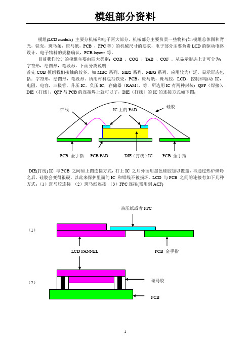
模组(LCD module) 主要分机械和电子两大部分,机械部分主要负责一些物料(如:模组总体图和背光,铁壳,斑马条,斑马纸,PCB ,FPC 等)的机械尺寸的要求,电子部分主要负责LCD 的驱动电路设计、电子物料的规格确认,PCB layout 等。
目前我们设计的模组主要由四大类别:COB 、COG 、TAB 、COF 。
从显示形态上计可分为:字符形,绘图形,笔段形。
下面分类说明:首先COB 模组我们接触的较多,如MBC 系列,MBS 系列,MBG 系列,应用较为广泛,显示形态包括:字符形,绘图形,笔段形。
所用材料包括铁壳,PCB ,斑马纸,斑马胶,LCD ,控制和驱动IC ,电阻,电容,三极管,升压IC ,负压IC ,存储器(RAM ),等,所选用IC 有两种封装:QFP (焊接),DIE (打线)。
QFP 与PCB 的连接焊上就可以了,DIE (打线)的IC 的连接方式如下图:DIE(打线) IC 与PCB 之间如上图连接方式,打上IC 之后外面用黑色硅胶加以覆盖,再通过热炉烘烤之后,硅胶会变得很硬,以此来保护里面的IC 和铝线不被损坏。
LCD 与PCB 之间的连接有如下几种方式:(1)斑马胶连接 (2)斑马纸连接 (3)FPC 连接(需用到ACF)(1)(2)在驱动方面,我们可以参照如下框图:以16*1 character 为例:KS0066(即S6A0069)为字符形模组LCD控制和驱动IC,它包括:16 Common 和40 Segment signal 输出,可以驱动8*2或16*1字符形模组,它有两种封装(80QFP and 80 DIE), 常与S6A0065(KS0065)或S6A2067(KS0063A)配合使用来驱动更多字符的LCD,我们最常用的字符形模组的控制IC :KS0066(S6A0069)和KS0070(S6A0070),驱动器:KS0065(S6A0065)和KS0063(S6A2067),KS0066上面有说过能单独驱动16*1字符或8*2字符,KS0070有16 COM 和80 SEG 输出,能单独驱动16*2字符;KS0065 、KS0063是只含驱动器,不含控制器,KS0065有40 channel 输出,KS0063 有80 channel 输出。
- 1、下载文档前请自行甄别文档内容的完整性,平台不提供额外的编辑、内容补充、找答案等附加服务。
- 2、"仅部分预览"的文档,不可在线预览部分如存在完整性等问题,可反馈申请退款(可完整预览的文档不适用该条件!)。
- 3、如文档侵犯您的权益,请联系客服反馈,我们会尽快为您处理(人工客服工作时间:9:00-18:30)。
符号 VDD -Vss VDD -V0 VI
Topr Tstg
最小值
-0.3 -0.3
-0.3
-20 −30
项目
输入高电压 输入低电压 输出高电压 输出低电压
电源电流
符号
VIH VIL VOH VOL IDD
条件
IOH=0.2mA IOL=1.2mA
VDD=5V
MIN
2.2 -0.3 2.4
运行时间(250Khz): 40 µs 功能:设置CG RAM地址。A5 ~ A0 = 0 ~ 3FH。 8、DD RAM地址设置
运行时间(250Khz): 40 µs 功能:设置DD RAM地址;
N = 0:一行显示,A6 ~ A0 = 0 ~ 4FH N = 1: 两行显示,首行A6 ~ A0 = 00H ~ 2FH ,次行A6 ~ A0 = 40H ~ 67H 9、读BF及AC值
得揭去,以免弄脏或损坏显示屏。 二、加装衬垫
在模块与前面板之间最好加装一块约0.1毫米左右的衬垫面板,还应保持平整,以免在装配后 产生扭曲,并可提高抗震性能。 三、严防静电
模块中的控制驱动电路是低压微功耗的CMOS电路,极易被静电击穿。静电击穿是一种不可修 复的损坏,而人体有时会产生高达几十伏或上百伏的高压静电,所以在操作、装配以及使用中都应 极其小心。要特别注意以下几点:
3. 模块使用时,接入逻辑电源和驱动电源的顺序,应是先逻辑电源,后驱动电源,断电时应 先驱动电源,后逻辑电源,这样做有助于保持屏的良好显示效果和避免在上电、断电时的电压冲击 损坏。所以推荐使用带控制的DC-DC电源做为模块的驱动电源。
4. 点阵液晶模块显示时的对比度、视角与温度、驱动电压关系很大,所以,如果VEE调整过 高,不仅会影响显示,还会缩短模块的使用寿命。
字符型液晶显示模块目前在国际上已经规范化,无论显示屏规格如何变化,其电特性和接口形 式都是统一的。因此只要设计出一种型号的接口电路,在指令设置上稍加改动即可使用各种规格的 字符型液晶显示模块。
第一章 注意事项
一、处理保护膜 在装好的模块成品表面贴有一层保护膜,以防在装配时沾污显示表面。在整机装配结束前,不
3
点阵字符型液晶显示模块使用手册
4. 不得修改导电胶条; 5. 不得修改任何内部支架; 6. 不要碰、摔、折曲、扭动模块。 五、焊接
在焊接模块外引线接口电路时应按如下规程进行操作 1. 烙铁头温度小于280°C 2. 焊接时间小于3~4s 3. 焊接材料共晶型低熔点 4. 不要使用酸性助焊剂 5. 重复焊接不要超过3次且每次重复需间隔5分钟 六、模块的使用与保养
液晶驱动电压:
4
RS
H/L
寄存器选择: 1: 数据寄存器; 0: 指令寄存器
5
R/W
H/L
读、写操作选择 1: 读; 0: 写
6
E
H,HÆL
使能信号 ENABLE
7
DB0
H/L
数据总线
8
DB1
H/L
数据总线
9
DB2
H/L
数据总线
10
DB3
H/L
数据总线
11
DB4
H/L
数据总线
12
DB5
H/L
数据总线
1. 模块的外引线决不允许接错,在您想调试液晶模块时,请注意正确接线,尤其是正、负电 源的接线不能有错,否则可能造成过流、过压,烧毁电路上的芯片等,对液晶模块元器件有损的现 象。
2. 模块在使用时,接入电源及断开电源必须在正电源稳定接入以后才能输入信号,电平如在 电源稳定前或断开后输入信号电平,有可能损坏模块中的IC及电路。
S/C = 0: 光标平移一个字符位; R/L = 1: 右移;R/L = 0:左移。 6、功能设置
运行时间(250Khz): 40 µs
1
1
0
功能:工作方式设置(初始化指令)。
0x38
其中:DL = 1:8位数据接口;DL = 0:4位数据接口;
11
点阵字符型液晶显示模块使用手册
N = 1:两行显示;N = 0:一行显示; F = 1:5 × 10点阵字符;F = 0:5 × 7点阵字符。 7、CG RAM地址设置
13
DB6
H/L
数据总线
14
DB7
H/L
数据总线
2、读、写操作
(1)写操作(MPU至HD44780/KS0066)
7
点阵字符型液晶显示模块使用手册
项目 使能周期 使能脉冲宽度 使能升降时间 地址建立时间 地址保持时间 数据建立时间 数据保持时间
(2)读操作
符号 TcycE Pweh Ter,Tef
5. 因为液晶材料的物理特性,液晶的对比度会随着温度的变化而相应变化,所以您加的负电 压值,应该随温度作相应的调整,大致是温度变化10°C 电压变化1伏。为满足这一要求,您可做 一个温度补偿电路或者安排一个电位器,随温度调整负电压值。
6. 不应在规定工作温度范围以外使用,并且不应在超过存储极限温度的范围。外存储如 果温度低于结晶温度,液晶就会结晶,如果温度过高,液晶将变成各向同性的液体破坏分子取向, 使器件报废。
Tah
10
-
ns
数据延迟时间
Tddr
-
320
ns
数据保持时间
Tdhr
10
-
ns
8
点阵字符型液晶显示模块使用手册
(3) 信号真值表 RS
0 0 1 1
R/W
0 1 0 1
E
下降沿 高电平 下降沿 高电平
功能
写指令代码 读忙标志和AC值
写数据 读数据
四、电特性
(1)绝对最大值范围 项目
电路逻辑电压(V) 液晶驱动电压(V) 输入电压(V) 工作温度(°C) 存储温度(°C)
7. 用力按压显示部分,会产生异常显示,这时切断电源稍待片刻,重新上电即恢复正常。 8. 液晶显示器件或模块表面结雾时,不要通电工作。因为这将引起电极化学反应,产生断线。 9. 长期用于阳光及强光下时,被遮部分会产生残留影像。
4
点阵字符型液晶显示模块使用手册
七、模块的存储 若长期(如几年以上)存储,我们推荐以下方式:
功能:读忙BF值和地址计数器AC值。 其中:BF = 1:忙; BF = 0:准备好。此时AC值意义为最近一次地址设置(CG RAM或
DD RAM)定义。 10、写数据
运行时间(250Khz): 40 µs 功能:根据最近设置的地址性质,数据写入DD RAM或CG RAM内。 11、读数据
运行时间(250Khz): 40 µs 功能:根据最近设置的地址性质,从DD RAM或CG RAM数据读出。
2、归位(返回) 运行时间(250Khz): 1.64 µs 功能:AC= 0, 光标、画面回HOME位。
10
点阵字符型液晶显示模块使用手册
3、输入方式设置
运行时间(250Khz): 40 µs 功能:设置光标、画面移动方式。 其中:I/D =1: 数据读、写操作后,AC自动增一;
I/D =0: 数据读、写操作后,AC自动减一; S = 1:数据读、写操作,画面平移; S = 0: 数据读、写操作,画面不动。 4、显示开关控制
0 --
最大值
7.0 13.0 VDD+0.3 +70 +80
TYP
----2.0
单位
V V V °C °C
MAX
VDD 0.6 VDD 0.4 3.0
单位
V V V V mA
9
点阵字符型液晶显示模块使用手册
第四章 字符型液晶显示模块指令集
一、指令集
1、清屏 运行时间(250Khz): 1.64 µs 功能:清DDRAM和AC值。
1. 装入聚乙稀口袋,最好有防静电涂层,并将口封住。 2. 在-10°C~ +35°C 之间存储。 3. 放暗处,避强光。 4. 决不能在表面压放任何物品。 5. 严格避免在极限温/湿度条件下存放。 八、责任范围及维修
在您购买液晶显示模块时我公司将会为您做显示模块的检测,确保您所买的显示模块为完好的 器件。在您使用过程中因不小心将显示模块损坏,您可送至我公司维修,如果出现屏被损坏的问题, 将无法进行修理,只能更换玻璃。我公司将收取成本费。
Tas Tah Tdsw Th
最小值 1000 450
140 10 195 10
最大值 25 -
单位 ns ns ns ns ns ns ns
项目
符号
最小值
最大值
单位
使能周期
TcycE
1000
-
ns
使能脉冲宽度
Pweh
450
-
ns
使能升降时间 Ter,Tef
-
25
ns
地址建立时间
Tas
140
-
ns
地址保持时间
1. 不要用手随意去摸外引线、电路板上的电路及金属框; 2. 如必须直接接触时,应使人体与模块保持在同一电位或将人体良好接地; 3. 焊接使用的烙铁和操作用的电动工具必须良好接地,没有漏电; 4. 不得使用真空吸尘器进行清洁处理,因为它会产生很强的静电; 5. 空气干燥也会产生静电,因此工作间湿度应在RH60%以上; 6. 取出或放回包装袋或移动位置时,也需小心防止产生静电,不要随意更换包装或舍弃包装。 四、装配操作时的注意事项 1. 模块是经过精心设计组装而成的,请勿随意自行加工修整; 2. 金属框爪不得随意扭动拆卸; 3. 不要随意修改加工PCB板外形、装配孔、线路及其部件;
2
点阵字符型液晶显示模块使用手册
前言
我公司字符系列LCM具有8 ×1~ 40 ×4 (字符×行)各种规格,广泛应用于智能仪表、通讯、 办公自动化及军工等领域。