约束管理器_allegro
Allegro_约束管理器-_Constraint_Manager
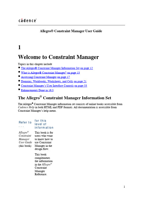
Allegro® Constraint Manager User Guide1Welcome to Constraint ManagerTopics in this chapter includeThe Allegro® Constraint Manager Information Set on page 12What is Allegro® Constraint Manager?on page 13Accessing Constraint Manager on page 17Domains, Workbooks, Worksheets, and Cells on page 21Constraint Manager’s User Interface Controls on page 33Enhancements Done in 16.3The Allegro® Constraint Manager Information SetThe Allegro® Constraint Manager information set consists of online books accessible from Cadence Help in both HTML and PDF formats. All documentation is accessible from Constraint Manager’s help menu.Refer to . . .for this level of informationAllegro®Constraint Manager User Guide (this book) This book is for users who want to know how to use Constraint Manager in the design flow. This book complements the information in the Allegro® Constraint Manager Reference.Allegro® Constraint Manager Reference This book contains descriptions and procedures for all commands, organized by menu-sequence. Information about worksheet cells is also included.If you click help in a dialog box or if you highlight a menu command and press F1, the appropriate command description from this book appears.This book complements the information in the Allegro® Constraint Manager User Guide.Allegro® Platform Constraints Reference This book contains information describing the constraints architecture, and it includes reference information for each constraint.Allegro® Platform System Connectivity Manager This book contains information describing the hierarchical,User Guide lower-levelconstraints usedin theConstraintManager-enabled, high-speed flow.What is Allegro® Constraint Manager?Allegro® Constraint Manager is a cross-platform, workbook- and worksheet-based application used to manage constraints across all tools in the Cadence PCB and IC Package design flow.Constraint Manager lets you define, view, and validate constraints at each step in the design flow, from design capture (in Allegro® Design Entry HDL or System Connectivity Manager) to floorplanning (in Allegro® PCB SI L, XL, and GXL to design realization (in Allegro®PCB L, XL, GXL, and OrCAD PCB Editor). You can also use Constraint Manager with SigXplorer to explore circuit topologies and derive electrical constraint sets which can include custom constraints, custom measurements, and custom stimulus.Note: Figure 1-2 depicts Constraint Manager worksheets as launched from PCB Editor, OrCAD PCB Editor, or APD. The worksheet hierarchy is different for Constraint Manager when launched in exploration mode, from Allegro Design Entry HDL, or from System Connectivity Manager.Figure 1-1 The Constraint Manager User InterfaceConstraint Manager uses familiar user interface controls. See Table 1-2on page 33 for more information.In Constraint Manager, you work with objects and constraint sets, which capture your design requirements.Constraint Manager organizes constraints and Constraint Sets into the Physical, Spacing, Same Net Spacing, and Electrical domains. You then assign the appropriate constraint set to objects in your design, changing references (or re-defining the currently assigned constraint set) as your design requirements change. A constraint set can be referenced by any number of objects in your design.For more information on design objects and the object hierarchy, see Chapter 2, “Working with Constraint Objects.”For more information on how to define constraint sets and how to assign them to objects in your design, see Chapter 3, “Working With Reusable Constraint Objects — CSets.”Constraint Manager affords you the following features and benefits:Table 1-1 Constraint Manager FeaturesFeature BenefitObject Grouping You can organize objects into easily-managed units, such as a Class, Bus, Differential Pair, or Match Group to make it easier to apply constraints to member objects.Conceptual Definition You can define constraints in a Constraint Set and later apply those constraints to net-related objects.Redefinable Constraints Rather than changing individual net-related constraints one-by-one, you can redefine a constraint set and all objects that reference that constraint set get updated all at once.Cross-Probing You can run Constraint Manager with companion tools such as Allegro Design Entry HDL, Allegro SI, or Allegro Package Design and select a net in ConstraintManager and see the associated object update dynamically in the schematic, floorplanner, or layout, respectively. Conversely, Constraint Manager updates its values when they are modified in a companion tool.When you cross probe cells that contain constraint violations, the respective DRC marker (bowtie) becomes highlighted in the design entry- or PCB-Editor, or in APD.Topology Exploration You can access SigXplorer from Constraint Manager to schedule pins and derive generic or net-specific constraints, which may include customconstraints,custommeasurements,and customstimulus. Theresultingtopologytemplate datacan be importedinto ConstraintManager as anElectrical CSet. Design Reuse You can groupconstraints thatsatisfy aspecific designrequirementinto anconstraint set,which can bereferencedwithin theactive design orexported forreuse in asubsequentdesign.Cloning Constraints In addition to importing constraint sets or creating them from scratch, you can copy it, modify its parameters, and save it under a new name.Analysis ConstraintManagerperforms designrule checks, andsimulations asnecessary, toanalyze thedesign.Analysis resultsarecommunicatedby DRC markers, results populated in worksheet cells, simulation waveforms, and reports. Analysis results (actuals) can be compared to defined constraints to derive margins.System-level Constraints Constraint Manager can capture board-to-board interconnect constraints.Persistent Storage Constraint Manager maintains constraint information in either the board or the schematic database.Net, Component, and Pin Properties The Properties workbooks let you add and edit certain properties for nets, components, or pins.Customizable User Interface You can create a custom workbook and worksheets that suit your work habits.Accessing Constraint ManagerYou access Constraint Manager in Exploration mode through the Windows Start menu or by entering consmgr in a Unix or Linux shell.Constraint Manager can also be invoked from a host tool as follows:From this tool Choose this menu commandAllegro PCB Editor, Allegro Package Design, or Allegro SI Setup – Constraints – Electrical Physical Spacing Constraint ManagerAllegro Design Entry HDL Tools – Constraints – EditSystem Connectivity Manager Design – Edit ConstraintsYou can also click the Constraint Manager icon in the host tool’s toolbar.Constraint Manager maintains constraint information in the board database when used with Allegro PCB or SI, in the package database when used with Allegro Package Design, or in the schematic database when used with Allegro Design Entry HDL.The appearance of the Worksheet Selector, worksheets, andcommands differ depending on whether Constraint Manager islaunched in Exploration mode, invoked from a front-end application,or a backend-application. For example, By Layer view of Physicaland Spacing cells is not available in Constraint Manager, whenlaunched from OrCAD PCB Editor or Allegro PCB Editor,Performance L option.The name of the tool from which you launch Constraint Manager appears in the banner atop the Constraint Manager user interface. For example:Constraint Manager (Connected to Allegro Design Entry HDL)See Chapter 6, “Using Constraint Manager with Other Tools Across the Allegro Platform”for using Constraint Manager with other Cadence tools.Constraint Manager launched from Allegro PCB Series L, Performance L,and OrCAD PCB EditorThis manual covers all functionality available in Constraint Manager when invoked from Allegro® PCB Series GXL and XL. When invoked from an Allegro® PCB Series L, Performance L, or OrCAD PCB Editor, Constraint Manager launches with these limitations:Scripting Scripting islimited to thecommands andconstraints thatare supported inAllegro® PCBSeries L orOrCAD PCBEditor.Match Groups You can define Match Groups only in net-level worksheets; you cannot define match groups at the Constraint Set-level.Pin Pairs You can definepin pairs only innet-levelworksheets; youcannot define pinpairs at the at theConstraint Set-levelSignal Integrity Signal integrity analysis is not supported. The Signal Integrity workbook has been removed.Timing Timing analysis isnot supported.The Timingworkbook hasbeen removed.Custom measurements Custom measurementsand custom stimulus and custom stimulus are not supported. The Custom Measurements tab (Analyze – Analysis Modes) has been removed; only the DRC Modes tab remains. The Custom Measurements workbook is not visible.Crosstalk DRC Crosstalk analysisis not supported.The max xtalkand max peak xtalk design rule checks have beenremoved from theAnalysis Modesdialog box.Topology Templates Topology import and export are not supported. As such, the Tools menu has also been removed prohibiting access to topology exploration tools including SigXplorer and SigWave.Analysis Simulation-basedanalysis is notsupported. Onlydesign rulechecks can beperformed.Xnet Creation You create anXnet (extendednet) through asignal model.using a Series XLor GXL PCBEditor or high tier legacy PCB Editor. PCBPerformanceSeries LIn the Electrical domain, custom measurements, pin delay, and Z-axis delay are not supported. You also cannot control same net crosstalk and parallelism checks.By Layer view of Physical and Spacing cells is not supported.Ratsnest Bundle worksheets are not supported.Microvias are not supported.PCB Series L In theElectricaldomain,custommeasurements,pin delay, andZ-axis delayare notsupported.You alsocannot controlsame netcrosstalk andparallelismchecks.For thePhysical- and Spacing-domains, regions, pin pairs, Xnets, differential pairs, buses, and by-layer worksheets are not supported.Ratsnest Bundle worksheets are not supported.Microvias are not supported.OrCAD PCBEditor By Layer view of Physical and Spacing cells is not available.Ratsnest Bundle worksheets are not supported.Microvias are not supported.When you select an object in Constraint Manager and right-click, a context pop-up menu appears. Keep in mind that this guide depicts all available options. If you launched Constraint Manager from Allegro® PCB Series L Editor (Performance), orOrCAD PCB Editor, some options will be removed or dimmed to inhibit functionality. Constraint Manager launched from Allegro® Physical ViewerPCB collaboration tools lack constraint management access, yet companies with co-design partners may require design constraint information as specified by contract or agreement. Use Constraint Manager in conjunction with Allegro® Physical Viewer as a back-end validation tool that lets design partners view electrical constraint information and analysis results and communicate it without requiring interpretation or conversion if an Allegro flow is used.When invoked from the Allegro® Physical Viewer Setup menu, read-only mode Constraint Manager launches with a limited functionality set. You can view the constraint information that a .brd file contains. All constraints appear in native delay values (for example, not a length only Performance mode). You cannot modify or export these constraints as certain menu functionality is disabled: right mouse buttons will not allow you to create, modify, ordelete objects. Print and View menu options are available.Read-only mode Constraint Manager includes all worksheets. However, SigWave or simulation actuals data are unavailable. Actual and Margin information is available for the constraints based on the design’s current state.Although Allegro® Physical Viewer does not let you change DRC modes, as they are inherited from the board, you can run DRC from Allegro to display actual data in Constraint Manager, which changes the database; then save it in Allegro® Physical Viewer. Domains, Workbooks, Worksheets, and CellsThe Constraint Manager workspace (see Figure 1-2, and Figure 1-3on page 23) contains the following components.The:Menus for command accessTool Bars for quick command accessSelector Bar for switching among domains and DRC and Properties WorkbooksW orksheet Selector for selecting the appropriate worksheetType column for identifying the type of object in the Objects columnW orksheets for capturing, editing, and validating constraintsS tatus Bar for feedback on object selection and constraint processingDRC Status indicator for checking the state of design rule checkingFigure 1-2 The Constraint Manager workspaceNote: When you select an object in Constraint Manager and right-click, you can also access commands from a context-sensitive, pop-up menu.The Status Bar provides key information about cell contents, the state ofobjects, error conditions, and conditions and processes in your design.When in doubt, consult the status bar.The Worksheet SelectorUse the W orksheet Selector to access the appropriate worksheet that you want to work in. Selector Bars let you access individual constraint worksheets, properties worksheets, and DRC worksheets, which you access by clicking on a Selector Bar. You can also undock and reposition the W orksheet Selector.Figure 1-3 Worksheet SelectorGrab the border of the W orksheet Selector and reposition it to get a fullview of workbook and worksheet selector nodes (as shown).Domain Selector BarsConstraint Manager organizes constraints, and constraint sets, by domain: Electrical, Physical, Spacing, and Same Net Spacing. You access each domain by clicking on the appropriate Selector Bar, which is located at the bottom of the W orksheet Selector (see Figure 1-3).Figure 1-4 Worksheet HierarchyIn the Constraint Set Folders for all domains, you define generic rules and you create generic object groupings. You can later assign these rules to the appropriate net-related objects in your design.In the Net folders for all domains, you can create net-specific object groupings, and you can define certain net properties. In the Electrical domain, you can also create a constraint set based on the characteristics of a net object.In the Physical, Spacing and Same Net Spacing constraint folders, worksheets based on layer, or by all layers, contain Nets, Classes, and Regions.By Layer view of Physical and Spacing cells is not available inConstraint Manager, when launched from OrCAD PCB Editor orAllegro PCB Editor, Performance L option.Properties Selector BarUse the Properties selector bar to manage net, component, and pin properties.The Net folder provides you with a quick glance of electrical and general properties. Some cells in these worksheets cannot be edited.The Component folder provides component coordinates, based on placement information, source data for third-party thermal analysis tools, and part definitions. Also included are electrical, thermal, and pin fabrication data. Some cells in these worksheets cannot be edited.System Connectivity Manager also provides component worksheetswhere you can define and edit these properties.See the Allegro Platform Properties Reference for more information on component properties.DRC Selector BarUse the DRC selector bar to view and waive design rule violations on objects inPCB Editor or APD. See the Objects – Waive command in the Constraint Manager Reference for more information.WorkbooksOnce you expand a parent Object Type folder, workbooks organize objects by design discipline. For example, the Electrical domain contains the Signal Integrity, Timing, Routing, and Custom Measurements workbooks. Also in the Electrical domain, the All Constraints workbook in the Electrical CSet folder consolidates constraints from all worksheets to give you a global view. Subordinate to the All Constraints workbook is the User Defined folder, which contains constraints that you have defined in SigXplorer. Note: The worksheet hierarchy is different if you launch Constraint Manager in exploration mode, or from Allegro® Design Entry HDL or Allegro® System Architect.When you select a workbook, all worksheets that belong to that workbook appear in a shared worksheet window. You can use the W orksheet Selector to select a worksheet or you can select a worksheet by clicking on the appropriate tab in the shared workbook window. You may have to scroll horizontally to locate the desired worksheet tab.Note: When you launch Constraint Manager from a physical layout editor, the cells that are in view are populated first. As you scroll other cells into view, the layout tool updates hidden cells as they become visible in Constraint Manager.The Analyze – Analysis Modes command controls DRC checks. Also, refer to the DRC State Bar, located at the bottom of Constraint Manager, adjacent to the Status Bar, tolearn the state of DRC updatesdetermine if DRCs are up-to-date for all enabled checksFigure 1-5 Workbooks and WorksheetsIn Figure 1-5, notice how the Net object type folder is expanded to show Timing as the active workbook. The Timing workbook contains the Switch/Settle Delays and Setup/Hold worksheets. Notice how the worksheets in the W orksheet Selector correspond to theworksheet tabs in the active workbook. Also notice that the active workbook and the active worksheet within the active workbook are emphasized with color in the workbook selector. Note: If any workbook has only one worksheet, Constraint Manager updates the W orksheet Selector to contain only the worksheet (under the Object Type folder).For information on objects and the object hierarchy, see Chapter 2, “Working with Constraint Objects.” For information on how to define CSets and how to assign them to objects in your design, see Chapter 3, “Working With Reusable Constraint Objects — CSets.”Physical and Spacing Workbook ViewsUnlike Electrical worksheets, Physical , Spacing, and Same Net Spacing CSet worksheets include layers, which correspond to the cross-section view of your design. Furthermore, you can view these layers collectively (All Layers ) or individually (By Layer ). You can also view them at the CSet-level or at the Net-level. See “All Layers / By Layer CSet Views” on page 28. and “All Layers Net View” on page 29.By Layer view of Physical and Spacing cells is not available inConstraint Manager, when launched from OrCAD PCB Editor orAllegro PCB Editor, Performance L option.Working in the CSet object folder lets you work in the abstract, defining CSets that will later be applied to net objects. The All Layers view shows CSets in collapsed form and layers associated with a CSet in expanded form. The By Layer view (in the CSet folder) shows layers in collapsed form and CSets associated with each layer in expanded form.Note: The CSet view does not have a Referenced CSet column.Figure 1-6 All Layers / By Layer CSet ViewsFigure 1-7 All Layers Net ViewWorking in the Net object folder lets you define CSets based on existing CSets or based on constraints already on Net objects. The All Layers view shows Container Net objects in collapsed form and Net objects in expanded form.Note: The Net, Net Class-Class (in the Spacing domain) and Region object types have a Referenced CSet column but do not have a By Layer viewSame Net Spacing DRC ModesAs with other domains, you enable design rule checks for all layers through the Analysis Modes dialog box. However, in the Same Net Spacing domain, you can control design rule checks by layer.You define a Same Net Spacing CSet in the CSet folder, and later assigning that CSet to a constraint object. In this way, you can enable or disable the CSet, effectively providing you with a granular level of control of setting constraint modes by layer. You do this by choosing TRUE or FALSE in the Enable DRC By-Layer column in the Options worksheet (see Figure 1-8).Note: A by-layer constraint check is a slave to the mode for that constraint as set in the Analysis Modes dialog box (choose Analyze – Analysis Modes). That is, if the individualDRC is not enabled in the Same Net Spacing Modes tab, Constraint Manager ignores the state of the Enable DRC By-Layer column.Figure 1-8 Layer-based DRC ModesCellsCells hold data, results, or calculations. Constraint Manager uses different colors or shades of color in cells depending on the state of your design and on the scope of the data in the cell.Indicates avalueinheritedfrom ahigher-levelobject, suchas a CSet.Indicates aPass state —A valueindicatingthat the cellfalls withinthe setconstraintlimit.Indicates aPass state —A valueindicatingthat all childcells of the parent object fall within the set constraint limit.Indicates a directly set value in a cell. Also called an override.Indicates a value that cannot be computed. The reason appears when you hover your mouse over a yellow cell and observe the message displayed in the status line, located at the lower-left corner of Constraint Manager. You may have not have . . .enabled the DRC mode for the cell completely placed the object completely routed the object correctly set up simulationparameters Note: You can set certain constraints, such as differential pairs, in more than one domain. Constraint Manager indicates a constraint edit in one domain by coloring the cell of the same constraint in the opposite domain yellow.Indicates a Fail state — A value indicating that the cell violates the set constraint limit. Constraint Manager rolls up worst-case Margins to higher-level objects.Indicates a Fail state –— A value indicating that any child cell of the parent object violates theset constraintlimit.Indicates acell which isnot applicableto the object.These cellsnever containvalues.Indicates acell that youcannot edit.Indicates acellcontaining aformula (thered bar to theright of thecell).Indicates acell that isbookmarked.To guide you in entering data into a cell, right-click in the cell and chooseChange from the pop-up menu.Constraint Manager’s User Interface ControlsConstraint Manager employs the same conventional window and worksheet controls that are used in Microsoft Windows Explorer® and Microsoft Excel®. Constraint Manager also supports the Microsoft Intellimouse® and wheel mouse.Table 1-2 User Interface ControlsTask Feature UsageCommand Access Pull-down Menus Click the pull-down menu atthe top ofConstraintManager toaccesscommands. Icons Click an icon toexecute aIf you brieflyhover thecursor above anicon, a tool tipdisplays in thestatus bar(located at thelower-leftcorner ofConstraintManager)describing theicon’s function. Keyboard Shortcuts Press Controland press:p (to print)z (to undo)c (to cut)v (to paste)f (to find)d (to delete)Also, you canaccess manycommands bypressing Altalong with theunderlinedcharacter, andyou can assignyour ownshortcuts (seethe Tools –CustomizeShortcut Keyscommand intheConstraintManagerReference).Right-Click (context sensitive)Depending on the object selected, you can right-click to quickly access aact on that object.Window and Worksheet Sizing and Placement Drag and Drop You can dragto repositionthe ConstraintManagerwindow, andindividualworksheets, onyour desktop. Sizing Borders You can resizethe ConstraintManagerwindow or anindividualworksheet openwithinConstraintManager bydragging theborder. Maximize/Minimize You canminimize anopen worksheetto an icon oryou canmaximize it tofocus only onthat worksheet. Dismiss You can clickthe dismiss [X]button (locatedat the top right-corner of theworksheet) toclose aworksheet.Constraint datais not lost whenyou dismiss aworksheet.Worksheet Viewing Window Select You can clickand drag on anopen worksheetto reposition it.You can useObject Expand/Collapse the worksheet selector to work at any object level in the hierarchy (from the system level to the pin pair level) by expanding [+] and collapsing [-] the object tree-structure. You can also choose Objects – Expand and Objects – Collapse from the pull-down menus to achieve the same effect.Cascade You can viewall openworksheetsarranged one-behind-the-other bycascading(Window –Cascade).ConstraintManager ordersWorksheets sothat each isselectable witha click of themouse. Theactive windowis placed in theforeground andis identifiableby an active(selected)border.Tile You can viewall openworksheetssimultaneouslyby tiling(Window –Tile). Eachopen worksheetis automaticallysized toaccommodatethe size of theConstraintManagerwindow.New Window You canduplicate thecontent of theactiveworksheet in anew window.This lets you tofocus yourview ondifferentobjects in thesameworksheet.Worksheet Tab Select When you expand a constraint discipline (signal integrity, timing, routing) from the worksheet selector, all objects within that discipline appear in a worksheet window. You then click a related tab to activate the desired worksheet.You may haveto scrollhorizontallyuntil thedesiredworksheet tabis visible.Synchronize Rows When youmodify rows ofthe worksheetin focus (forexample,scrolling downor expanding abus),ConstraintManagerpromotes thesamemodification toall worksheetsthat havesynchronizationenabled.Accelerator KeysConstraint Manager provides function keys and modified function keys that provide quick access to common functions.Function KeysViewCntrl+F6OptionsRename F2Print Cntrl+pAnalysisCntrl+F9ModesAnalysisShift+F9SettingsAnalyze F9Find Cntrl+fFind Next F3FindShift F3 PreviousOpen a newCntrl+n window onthe activeworksheetCntrl+Tab Move to thenext openworksheetShift+Cntrl+Tab Move to thepreviousopenworksheetNextF6worksheettabPreviousShift+F6 worksheettabCntrl+F4 Close theactiveworksheetSelect aShift+Click contiguousrange ofcellsCntrl+Click Select anon-contiguousrange ofcellsAlt+ or Num+ Expandobject rowsCollapseAlt- or Num- object rowsCut Cntrl+x orShift+Del Copy Cntrl+c orCntrl+Ins Paste Cntrl+v orShift+Ins Delete anD elobject orcell content。
ALLEGRO约束设置

ALLEGRO约束规则设置介绍目录:第一部分:差分对的约束设置 (1)第二部分:非差分信号约束设置 (8)第三部分:区域约束设置 (11)第四部分:XNet等长设置 (12)本文所有操作与设置均在Allegro PCB editor 15.5环境中进行。
第一部分:差分对的约束设置下面我们将通过对LVDS差分对信号的约束设置分步骤的讲解各个设置过程,其约束条件如步骤1:全局约束设置。
在PCB editor界面下,点击“Setup→Constraints”或点击图标打开“Constraints Sys”窗口,将出现下图所示窗口。
点击“Set standard values”,弹出“Default values form”界面,在此可设置默认值,且窗口中所有设置值各自分属于spacing rule 和Physical rule 中名为“Default”的约束集。
此处我们取默认值。
图1下面步骤2-步骤4为Physical(Line/vias)rule物理特性(线宽和过孔)约束设置过程步骤2:线宽约束设置。
点击“Physical(Line/vias)rule set→set values”,在出现的窗口上方空白处填入新约束名称,如“LVDS_SIG”,然后点击“ADD”,新的约束就产生了。
如果需要设置这是某一层的约束,还要在“subclass”中选择相应的层面。
接下来就在相应栏填入需要的值。
如下图所示:图2如果还有其它信号的线宽要求,请重复上述步骤。
Min line width:最小线宽Max line width:最大线宽,填0=∞Min neck width:Neck 模式最小线宽Max neck length:Neck 模式最大走线长度DiffPair primary gap:首选差分间距(单端线可不填)DiffPair neck gap:Neck 模式差分间距(单端线可不填)过孔规格在“Via list property”中设定,一般设定在默认约束规则下。
allegro差分线分组约束规则设置
allegro差分线分组约束规则设置(最新版)目录1.allegro 差分线分组约束规则的概念2.allegro 差分线分组约束规则的设置方法3.allegro 差分线分组约束规则的应用实例4.allegro 差分线分组约束规则的优缺点正文一、allegro 差分线分组约束规则的概念Allegro 是一种用于印刷电路板(PCB)设计的专业软件,它能够帮助设计人员快速高效地完成电路板的布局和设计。
在 Allegro 中,差分线分组约束规则是一种用于控制差分线(differential pair)布局的规则,能够有效地提高电路板的信号完整性。
二、allegro 差分线分组约束规则的设置方法在 Allegro 中,设置差分线分组约束规则的方法如下:1.打开 Allegro 软件,点击菜单栏的“工具”选项,选择“约束管理器”。
2.在弹出的“约束管理器”窗口中,选择“新建”选项,创建一个新的约束。
3.在“新建约束”对话框中,选择“差分线分组”选项,然后输入差分线的名称和描述。
4.在“差分线分组”对话框中,设置差分线的属性,包括线宽、间距、层数等。
5.确认设置后,点击“确定”按钮,完成差分线分组约束规则的设置。
三、allegro 差分线分组约束规则的应用实例在实际的电路板设计中,差分线分组约束规则可以应用于各种需要差分线布局的场景,例如高速信号传输、模拟信号处理等。
下面是一个应用实例:假设我们需要设计一个用于高速数据传输的电路板,其中涉及到一对差分线。
我们可以通过设置差分线分组约束规则,控制这对差分线的布局,以确保信号的完整性。
四、allegro 差分线分组约束规则的优缺点差分线分组约束规则在提高电路板信号完整性方面具有显著的优势,但也存在一些不足之处:优点:1.有效提高信号完整性,减少信号干扰和噪声。
2.便于设计和修改,提高设计效率。
缺点:1.需要对差分线进行专门的设置和管理,增加了设计复杂度。
2.对于复杂的电路板设计,差分线分组约束规则的设置可能会变得繁琐。
Allegro操作说明(中文) Word 文档
26、非电气引脚零件的制作1、建圆形钻孔:(1)、parameter:没有电器属性(non-plated)(2)、layer:只需要设置顶层和底层的regular pad,中间层以及阻焊层和加焊层都是null。
注意:regular pad要比drill hole大一点27、Allegro建立电路板板框步骤:1、设置绘图区参数,包括单位,大小。
2、定义outline区域3、定义route keepin区域(可使用Z-copy操作)4、定义package keepin区域5、添加定位孔28、Allegro定义层叠结构对于最简单的四层板,只需要添加电源层和底层,步骤如下:1、Setup –> cross-section2、添加层,电源层和地层都要设置为plane,同时还要在电气层之间加入电介质,一般为FR-43、指定电源层和地层都为负片(negtive)4、设置完成可以再Visibility看到多出了两层:GND和POWER5、铺铜(可以放到布局后再做)6、z-copy –> find面板选shape(因为铺铜是shape)–> option面板的copy to class/subclass选择ETCH/GND(注意选择create dynamic shape)完成GND层覆铜7、相同的方法完成POWER层覆铜Allegro生成网表1、重新生成索引编号:tools –> annotate2、DRC检查:tools –> Design Rules Check,查看session log。
3、生成网表:tools –> create netlist,产生的网表会保存到allegro文件夹,可以看一下session log内容。
29、Allegro导入网表1、file –> import –> logic –> design entry CIS(这里有一些选项可以设置导入网表对当前设计的影响)2、选择网表路径,在allegro文件夹。
Allegro16.6约束管理器及使用示例
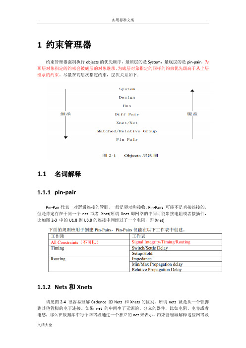
Allegro16.6约束管理器及使用示例1约束管理器约束管理器强制执行objects的优先顺序,最顶层的是System,最底层的是pin-pair。
为顶层对象指定的约束会被底层的对象继承,为底层对象指定的同样的约束优先级高于从上层继承的约束。
尽量在高层次指定约束,层次关系如下:1.1名词解释1.1.1pin-pairPin-Pair代表一对逻辑连接的管脚,一般是驱动和接收。
Pin-Pairs 可能不是直接连接的,但是肯定存在于同一个net 或者Xnet(所谓Xnet即网络的中间可能串接电阻或者接插件,比如图2-3 中的U1.8到U3.8的连接中间经过了一个电阻,即Xnet)1.1.2Nets和Xnets请见图2-4 很容易理解Cadence 的Nets 和Xnets的区别。
所谓nets 就是从一个管脚到其他管脚的电子连接。
如果net 的中间串了无源的、分立的器件,比如电阻、电容或者电感,那么在数据库中每个网络段通过一个独立的net来表示。
约束管理器解释这些网络段作为相邻的扩展的网络或者Xnet,Xnets在多板连接的结构中也可以贯穿连接器和电缆。
可以将Nets 和Xnets与ECSets 联系起来。
1.1.3Match GroupsMatch Group 是nets,Xnets或者pin-pairs 的集合,此集合一定要都匹配(delay 或者length)或者相对于组内的一个明确的目标。
如果delta 值没有定义,组内的所有成员都将是绝对匹配的,并允许有一定的偏差。
如果定义了delta 值,那么组内所有成员将相对匹配于明确的目标网络。
1.2在线检查设置首先在约束管理器中需要进行以下设置Analyze -> Analysis Modes这样在布线后,在相应的地方都会显示线长或约束相差值;如下图1.3示例通过一个实例来理解约束管理器U1看作是MCU,U2为DDR,ADDR0-3为地址线,需要作等长处理;CLK为时钟线,差分处理;U3,U4为连接同一个MCU的DDR;地址线是复用的,设置通过T型网络连接;需要作等长处理U5为DDR,DDR_DQ0-3为数据线,需要作等长处理1.3.1差分对约束即上图中的DDR_CLKP,DDR_CLKN设置Electrical ->Electrical Constraint Set -> Differential Pair 在Object的Name下方Project右键Create -> Electrical CSet;并输入参数差分对约束参数主要有以下几个:Min line spacing:内间距最小线距,若实际走线内间距小于这个值,DRC就会出错。
Allegro约束管理器(BACK-END)介绍
Allegro约束管理器(BACK-END)介绍一、约束管理器(BACK-END)在HDL的相应课程中约束是表格代替PCB中的Constraints设置让人容易理解,这里用SigXplorer图形化可以更深刻的理解约束的定义和为什么。
(一)、规划网络(根据Cadence教程)1、简单规划:选取要操作的网络显示:Display/Blank Rats/All隐藏所有的网络,打开约束管理器,Display/Show Rats/Net切换到约束管理器,Net…Wiring…选择要编辑的网络,右键菜单中选择Select,回到PCB后Done如下图:Logic/Net Schedule,比如要改为星形网络,点取左边端点移动时随之移动,在中部引脚处点下,再到最上方,回到中央再点下,下移在适当处点右键,选取Insert T点取放置点。
从该点拉向另一端点,再拉回到T点然后依此到其它点如下图,在等距时网线会隐藏:切换到约束管理器,该网络的拓扑显示为Userdefine,以该NET 创建一个ECSets如:a_constraints它会在ECS的Wiring中显示为Template。
点取其它网络,指定a_constraints为基参考ECSets。
OK后,在参考ECSets栏中可能出错(变为红色),鼠标放其上边在状态栏有出错信息,表明Mapping失败。
出错的应取消,方法是点选所有出错的,右键菜单中选择Clear。
在Analysis Mode中选中Net Shedule和Online DRC 。
在Verify Schedule列中为每个Net打开Yes。
按F9开始分析。
可以看到上图中所有网络都继承了网络的规划,这个影响走线因此效果远比原来的好。
也可以在System级(即ECSets)中加入Verify Schedule=Yes。
2、进阶:在PCB中先选取一组相似的网络创建一个BUS(在HDL的约束管理器是不能创建BUS的),在PCB中创建BUS来管理ECSets是一种快捷的方法。
Allegro中的约束规则设置1.1

A llegro中的约束规则设置Allegrophan修订记录日期版本描述作者2008-12V1.0初版,刚学完时的总结Allegrophan 2009-08V1.1小改,修改部分措辞Allegrophan目录一:Physical(Line/vias)rule物理特性(线宽和过孔)约束设置: (4)1)“Set values”设置约束特征值 (5)2)“Attach property”绑定约束 (6)3)“Assignment table”约束规则分配 (8)二“Spacing rule”间距约束设置 (9)1)“Set values”设置约束特征值 (9)2)“Attach property”绑定约束 (10)3)“Assignment table”约束规则分配 (11)三Constraint areas区域约束设置 (12)四Allegro中走线长度的设置 (13)1)差分线等长设置 (13)2)一组Net等长 (16)3)XNet等长 (17)线宽、线距、区域的约束主要在“Constraints Sys”中设置,点击“Setup/Constraints”或点击图标打开“Constraints Sys”窗口,如下:nded “Constraints Sys”窗口分两个级别,第一级别有两类:Standard design rules和ExteExtended design rules。
Standard design rules仅有一级分类,点击“Set standard values”设置默认约束值,如下:这里可以设置默认值,窗口中所有设置值各自分属于spacing rule和Physical rule中名为“Default”的约束集。
“Extended design rules”下一级分为三类不同约束设置:Spacing rule间距约束设置、Physical(Line/vias)rule物理特性(线宽和过孔)约束设置和Constraint areas区域约束设置。
高速PCB设计软件allegro16.6版本约束管理界面讲解
高速PCB设计软件allegro16.6版本约束管理界面讲解cadence约束管理器在PCB设计规则设置中是必不可少的,它也称为DRC检查规则,用来确定电路板的走线规则是否符合PCB设计要求。
本节主要是给大家介绍约束管理器的5个界面。
首先,可以通过菜单Setup/constraints/Constraint Manager…或者点击图标g进入约束管理器。
电气规则设置界面Electrical:电气规则设置选项,在Electrical Constraint Set中设置不同的电气规则,在Net 下将前面的规则赋予需要的网络物理规则设置界面Physical:物理规则设置选项,在Physical Constraint Set中设置不同的物理规则,在net 下将前面的规则赋予需要的网络;其中Region 是区域规则,主要针对BGA、引脚间距小、出线密度高的器件,需绘制一个区域框并赋予区域规则,区域内线宽和间距都可能小于区域外,物理规则下能够赋予物理规则。
间距规则设置界面Spacing:间距规则设置选项,在Spacing Constraint Set中设置不同的物理规则,在net 下将前面的规则赋予需要的网络,Net Class-Class是设置网络类之间的间距,补充网络间距之间的不足。
Region中可以赋予区域间距规则。
同名网络间距规则设置界面Same Net Spacing:同名网络间距设置选项,即一个网络本身之间的间距,主要是在需要绕线时运用。
属性设置界面DRC界面DRC:DRC错位查看选项,能够查看不同规则下错误的数量和位置,以及和错误相关的规则约束条件。
对高速PCB设计软件cadence16.6版本约束管理器界面进行介绍完毕后,下期继续为大家介绍与网络有关的约束与规则的讲解。
Allegro PCB设计中的约束管理
Allegro PCB设计中的约束管理本章主要介绍一下约束管理器的使用,约束管理器贯穿于原理图设计、PCB 设计、仿真分析设计,这里主要讲述在PCB Editor中如何使用约束管理器来对信号进行约束设置。
一、约束管理器概述约束管理器是贯穿于整个PCB设计平台的一个对信号约束的工具,在整个项目的开发过程中,起着桥梁的作用。
我们可以在原理图设计阶段在约束管理器中设定约束来指导PCB设计;也可以在使用仿真分析工具仿真后,将仿真分析的拓扑添加到约束管理器中从而来驱动布局、布线。
约束管理器是以表格形式为基础的工作表形式,所以其操作简单、运用灵活。
它将印制电路板所有的网名以表格形式显示,不仅使设计者对网名一目了然且更加方便地对信号设定不同的规则。
对不同的规则如相对长度规则、总长度规则、曼哈顿长度规则等分了不同的栏显示以方便大家的规则设定。
二、约束管理器1、约束管理器的启动在Allegro PCB Design中,选择菜单命令Setup/Electrical ConstraintSpeadsheet或者单击Setup工具栏中的按钮,打开约束管理器,如图10_1所示。
10_12、约束管理器界面概述1)菜单栏约束管理器的菜单栏包括:File、Edit、Objects、Column、View、Analyze、Audit、Tools、Window及Help。
2)Electrical Constraint Set栏此栏主要是对电气规则来设定约束,包括:Signal Intergrity(信号完整性设置规则)、Timing(时序规则设置)、Routing(布线设置)、All Constraint(所有的约束管理)。
3)Net栏Net栏主要对指定的网络来设置不同的约束规则,包括Signal Intergrity(信号完整性设置规则)、Timing(时序规则设置)、Routing(布线设置)、Custom Measeurement(用户添加规则管理)、General Properties(通用属性设置)。
allegro中如何设置class与class的规则
在Allegro中,设置类与类的规则通常涉及到约束管理器(Constraint Manager)的使用。
约束管理器是Allegro提供的一个强大的工具,用于定义、管理和应用各种约束,如物理约束、间距约束、高级约束等。
以下是如何在Allegro中设置类与类的规则的一般步骤:1. 启动约束管理器:在Allegro中,首先需要打开约束管理器。
这通常可以通过菜单栏的“工具”->“约束管理器”来完成。
2. 创建或编辑类:在约束管理器中,你可以创建新的类或编辑现有的类。
类是用来定义一组对象的约束规则的。
3. 设置类与类的规则:选择目标对象:首先,选择你想要应用约束的第一个对象或一组对象。
添加约束:在约束管理器中,选择适当的约束类型(例如,物理约束、间距约束等)。
设置参数:为所选约束设置适当的参数,例如距离、角度等。
关联类:为所选的约束指定一个或多个类。
这意味着你正在为一个或多个特定的对象组设置规则。
4. 应用约束:一旦你设置了所需的规则和参数,你可以将这些约束应用到你的设计中。
这通常是通过选择“应用”或“确定”按钮来完成的。
5. 验证和查看结果:在你应用约束之后,你可以通过验证工具来检查设计的合规性。
验证工具可以帮助你确定设计是否满足了你设置的约束条件。
6. 更新和编辑:随着设计的进行,你可能会需要更新或编辑这些约束。
你可以随时返回到约束管理器中进行这些更改。
7. 导出和导入:对于大型项目,你可能需要与其他团队成员共享这些约束。
Allegro 允许你导出这些约束到一个文件中,然后导入到其他Allegro项目中。
8. 使用脚本自动化:对于更高级的用户,Allegro还支持使用Tcl/Tk脚本来自动化和定制化这些过程。
科通集团_Cadence_Allegro_基础培训_第三期

• Line(布线)线宽和Layer(层)约束
– 间距约束(Spacing Constraint)
• 不同Net(网络)的Lines、Pads、Vias、Shapes之间的间距
– 相同网络间距约束(Same Net Spacing Constraint)
38
科通集团
/
电气约束(Electrical Constraint)
• Relative Propagation Delay工作表
39
科通集团
/
电气约束(Electrical Constraint)
间距约束(Spacing Constraint)
• 层间约束(Constraint By Layer)
28
科通集团
/
Same Net Spacing Constraint
• 设置和Spacing约束操作一样,注意是相同网络的对象之 间的间距。
29
• 创建Relative Propagation Delay约束(方式二)
45
科通集团
/
电气约束(Electrical Constraint)
• 创建Relative Propagation Delay约束(方式二)
46
科通集团
/
科通集团
/
物理约束(Physical Constraint)
• 为Net Class添加 Physical约束
方 法 一
18
科通集团
/
物理约束(Physical Constraint)
• 为Net Class添加 Physical约束
/
间距约束(Spacing Constraint)
约束管理器_allegro(16.3非常详细的资料)

allegro目录第一章约束管理器介绍 (4)1.1 约束管理器简介 (4)1.2 约束管理器界面简介 (8)1.2.1worksheet selector (8)1.2.2用户接口 (9)1.2.3View选项 (9)1.3 启动约束管理器 (11)第2章OBJECTS介绍 (12)2.1 P IN-P AIRS (13)2.1.1Pin-Pair规则 (14)2.2 N ETS和X NETS (14)2.3 B USES (15)2.4 M ATCH G ROUPS (15)2.4.1如何确定target pin pair (16)2.4.2相对/匹配的群组规则 (16)2.5 D IFF P AIRS (16)2.5.1差分对工作表 (17)2.5.2差分计算器(Differential Calculator)的使用方法 (19)2.5.3差分对规则 (19)2.6 D ESIGNS AND S YSTEMS (20)第3章设置网络的走线约束 (21)3.1.1设置网络的最大最小传输延迟 (21)3.1.2设置网络相对传输延迟 (24)3.1.3设置差分对约束 (26)3.1.4查看网络规范格式和物理格式 (28)第4章设置网络的时序和信号完整性约束 (30)4.1 设置时序约束 (30)4.2 设置信号完整性约束 (32)4.2.1设置电气属性约束 (32)0 第一章约束管理器介绍2 4.2.2设置反射属性约束 (33)第5章电子约束创建和应用 (35)5.1 创建ECS ET (35)5.2 指定ECS ET给网络 (40)5.3 不考虑ECS ET的缺省约束值 (41)5.4 在原理图中查看ECS ET (41)第6章ECOS实现 (43)6.1 在原理图中增加网络 (43)6.2 在原理图中修改约束 (45)6.3 在约束管理器中修改约束 (46)6.4 在约束管理器中删除约束 (46)6.5 在原理图中重新命名网络 (47)第7章在原理图和PCB之间同步约束 (50)7.1 从原理图中输出约束 (50)7.2 在PCB D ESIGN中查看和添加约束 (50)7.3 在原理图中导入并查看约束 (51)7.4 在PCB和原理图之间同步约束的两种模式 (52)7.4.1用原理图中的约束重写PCB中的约束 (53)7.4.2在原理图中导入PCB中变更的约束 (56)第8章约束分析 (58)8.1 查看工作表单元格和对象 (58)8.2 定制约束、定制测量和定制激励 (59)8.2.1定制约束 (59)8.2.1.1 用户定义的属性 (59)8.2.1.2 约束的定制测量 (59)第9章SCHEDULING NETS (61)9.1 S CHEDULING N ETS (61)9.2 S CHEDULING N ETS-R EVISITED (65)第10章相对传输延迟 (68)约束管理器简介第11章MATCH DELAY (73)第12章解决DRC冲突 (74)第13章约束管理器 (76)13.1 层次设计中的电子约束 (76)30 第一章约束管理器介绍4第一章约束管理器介绍约束管理器是一个交叉的平台,以工作簿和工作表的形式在Cadence PCB设计流程中用于管理所有工具的高速电子约束。
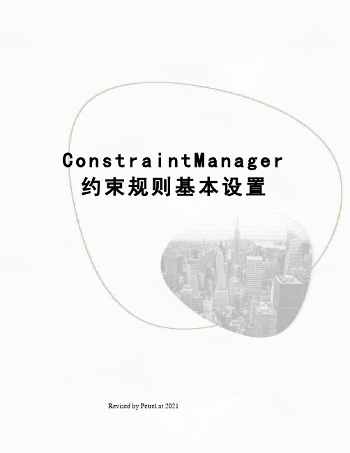
ConstraintManager约束规则基本设置
C o n s t r a i n t M a n a g e r约束规则基本设置 Revised by Petrel at 2021约束规则的设置孙海峰在PCB设计中规则设置是必不可少的,它也可以被称为DRC检查规则,用来确定电路板的走线规则是否符合设计要求。
在AllegroPCB的电路板设计过程中,设计约束规则主要包括时序规则、走线规则、间距规则、信号完整性规则等以及物理规则等设置。
首先,需要认识一下,AllegroPCB的约束管理器:在PCB设计界面中,执行Setup/Constraints/ConstraintManager命令,弹出AllegroConstraintManager对话框,如下图。
在约束管理器中,设计者可以对电路板的电气规则、物理规则、间距规则等设计规则进行设置定义。
约束规则可以按板层、网络或者区域进行设置。
约束管理器是Cadence系统提供的专用规则设置系统,主要有菜单栏、工具栏、工作表选择区、工作状态报告栏四部分,在工作表中选择一个对象,然后右击,在弹出的命令菜单中,可以进行任意操作。
工作表选择区内可以选择电气规则、物理规则、间距规则等规则设置。
在对应Net文件夹内,可以创建指定网络的对象分组,如:系统、设计、总线、差分对、扩展网络(XNet)、网络、相对或匹配群组,也可以创建基于相关属性的电气规则(ECSet)、物理规则(PCSet)、间距规则(SCSet)等。
约束管理器的约束对象分为引脚对、总线和匹配群组,她们相互之间存在优先级差异,即底层对象会集成顶层对象指定约束,为底层对象指定的约束优先高于上层继承的约束,对象层次的优先级为系统、设计、总线、差分对、扩展网络、相对或匹配群组、引脚对。
一、电气规则设置在约束管理器中,选择Electrical选项卡,其中可以为设计或网络来设置时序规则、信号完整性规则、布线的电气规则(延时、差分对)等,执行Objects/Create/ElectricalCSet命令可新建电气规则。
ALLEGRO培训包设定指定元件或网络约束规则标准版文档

A将L约LE束G规RO则约添束加管到理n器et上
将在约进束 行规高则速添布加线到时,ne一t上般都需要进行线长匹配,这时我们就需要设置好 constraint 规则,并将这些
在规进则行 分高配速到布各线类时ne,t 一gr般ou都p需上要。进行线长匹配,这时我们就需要设置好 constraint 规则,并将这些
上述步骤完成后,我们就要将已经设好的约束分配到这些 net group 上。
10
பைடு நூலகம்
ADLDLREG地R址O约线束,管片理选器线,和其他控制线的 NET_PHYSICAL_TYPE 设为DDR_ADDR.
点在击allpehgyrosic中al设ru置le不s同et的中约的束attach……,再点击右边控制面板中的 more
将下约面束 以规dd则r为添例加,到具ne体t上说明这些约束设置的具体步骤。
规 点则击分ph配y到sic各al类runleetsegtr中ou的p a上tt。ach……,再点击右边控制面板中的 more
将找约到束ck规n0则和添c加kp到0,ne点t上击 apply
DDR 地址线 、,片片选选及线其,他和控其制他线控:制线线宽的5mNilE,T_内PH部Y间SI距CA1L5_mTYiPl,E 外设部为间DD距R2_A0mDDil,R.应走成菊花链状拓
将 同约理束,规 可则 以添 将加D到DRn数et据上线,数据选通线和数据屏蔽线的 NET_PHYSICAL_TcYkPpE 设0,为 D点DR击_DATA,
点在击al右leg边ro控中制设面置板不中同的的m约or束e弹出的对话框 点AL击LE右G边RO控约制束面管板理中器的 more弹出的对话框
apply
DDR 数据线,ddrdqs,ddrdm线:线宽
Allegroxxx约束规则设置
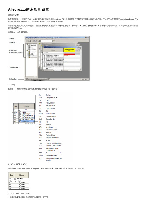
Allegroxxx约束规则设置约束规则设置约束管理器是⼀个交叉的平台,以⼯作簿和⼯作表的形式在 Cadence PCB设计流程中⽤于管理所有⼯具的⾼速电⼦约束。
可以使⽤约束管理器和SigXplorer Expert 开发电路的拓扑并得出电⼦约束,可以包含定制约束、定制测量和定制激励。
所谓约束就是⽤户定义的限制条件,当在板上⾛线和放置元件时会遵守这些约束。
电⼦约束(ECSets)就是限制PCB 上与电⾏为有关的对象,⽐如可以设置某个⽹络最⼤传输延迟为2ns。
以下图为⼀约束设置窗⼝。
⼀、说明先解释⼀下约束的类型以及约束中⽤到的简写名词,如下图所⽰:1、NCIs(NET CLASS)由众多nets或者buses、differential pairs、Xnet所组成的类,可对其赋予相似的约束。
如下图所⽰。
2、NCC(Net Class-Class)⼀般⽤在约束组与组之间的间距的时候使⽤,如下图。
3、DPr(Differential Pairs)差分对⼀组差分对⼀般由两条Xnet或者net以差分⾛线的⽅式组成,如下图。
差分对的形成有两种⽅式:⼀是由模型指定的差分对,再者就是由⽤户⾃⼰定义的差分对。
模型定义的差分对:可以在器件信号模型中指定差分对,可以使⽤PCB Design,PCB SI,SigXplores 来将模型指定给相应的元件。
⽤户定义的差分对:可以在约束管理器中 Net ⼀级的对象中创建差分对,可以灵活的更改差分对命名和更改差分对成员,但是没有模型指定差分对的精确性。
以下是设置差分对规则时,需要赋予约束的项。
针对以上约束中⽤到的⼀些约束点进⾏解释说明:差分对的worksheets包含5个主要的约束⽬录:(1)Pin Delay此值指⼀对⽹络之间管脚封装上的延迟,单位是时间ns 或者长度mil。
(2) 不耦合长度(Uncoupled Length)不耦合长度约束是⽤来限制差分对的⼀对⽹络之间的不匹配长度。
Allegro约束规则设置

约束规则的设置孙海峰在PCB设计中规则设置是必不可少的,它也可以被称为DRC检查规则,用来确定电路板的走线规则是否符合设计要求。
在Allegro PCB的电路板设计过程中,设计约束规则主要包括时序规则、走线规则、间距规则、信号完整性规则等以及物理规则等设置。
首先,需要认识一下,Allegro PCB的约束管理器:在PCB设计界面中,执行Setup/Constraints/Constraint Manager命令,弹出Allegro Constraint Manager对话框,如下图。
在约束管理器中,设计者可以对电路板的电气规则、物理规则、间距规则等设计规则进行设置定义。
约束规则可以按板层、网络或者区域进行设置。
约束管理器是Cadence系统提供的专用规则设置系统,主要有菜单栏、工具栏、工作表选择区、工作状态报告栏四部分,在工作表中选择一个对象,然后右击,在弹出的命令菜单中,可以进行任意操作。
工作表选择区内可以选择电气规则、物理规则、间距规则等规则设置。
在对应Net文件夹内,可以创建指定网络的对象分组,如:系统、设计、总线、差分对、扩展网络(XNet)、网络、相对或匹配群组,也可以创建基于相关属性的电气规则(ECSet)、物理规则(PCSet)、间距规则(SCSet)等。
约束管理器的约束对象分为引脚对、总线和匹配群组,她们相互之间存在优先级差异,即底层对象会集成顶层对象指定约束,为底层对象指定的约束优先高于上层继承的约束,对象层次的优先级为系统、设计、总线、差分对、扩展网络、相对或匹配群组、引脚对。
一、电气规则设置在约束管理器中,选择Electrical选项卡,其中可以为设计或网络来设置时序规则、信号完整性规则、布线的电气规则(延时、差分对)等,执行Objects/Create/Electrical CSet命令可新建电气规则。
1、选择信号完整性仿真规则Signal Integrity属性,其中包括电气属性、反射属性、单调失真属性、初始串扰、仿真串扰以及同步开关噪声这六个规则设置。
Allegro16.6约束规则设置详解2

7.2、过电阻的XNET 等长这里关键是设置XNET。
假设有一排过电阻的线需要等长。
首先创建电阻模型。
单击Signal Model 图标,如下图所示点击电阻,如下图所示,单击RN0603 10所有这种模型的电阻都高亮了,如下图所示单击Create Model。
按钮。
默认,单击OK默认单击OK。
如下图所示。
再单击OK 结束命令。
假设我们要将DR_MD49 到DR_MD53网络等长。
打开约束管理器,选择相对延迟,这里可以看到我们刚才设置的XNET。
我们在DR_MD49 网络上右键创建PIN PAIR选择2 个端点,如上图所示,单击OK。
同理,其他需要设置等长的网络,也创建PIN PAIR。
然后按住Ctrl 键选择这些PIN PAIR,右键创建MATCH GROUP 如下图所示设定约束值,及目标网络,方法同不过电阻网络等长设置。
7.3、T 型等长T 型等长设置,比如两个D DR 之间的等长就属于T 型等长,设置方法如下(以text_drr 举例)。
首先添加T 型连接点。
点击Logic-Net Schedule,单击你要设置网络的一个pin。
如下图。
在中间右键Insert T,加入T 型连接点,如下图所示然后去点击第二个pin,再回到T 型连接点,然后去点击第三个pin,右键done 即可。
创建的T 型连接点如下图所示这只是创建了一个网络的T 型连接点,如果需要创建多个,可点击进入约束管理器设置。
在N et-Routing——Wiring 下面,刚才设置的网络拓扑便会显示成UserDefined。
如下图所示选中那个网络,右键创建Creat-Electrical CSet,如下图然后将你需要设置T 型结构的网络选择刚才设置的ECSet 作为参考,Verify Schedule 选择yes 即打开验证,如下图所示。
然后打开检查模式,在约束管理器Analyze-Analysis Modes弹出的对话框中,将Stub length/Net 的检查模式选择为on 如下如所示。
Allegro16.6约束管理系统器及使用示例

1约束管理器约束管理器强制执行objects的优先顺序,最顶层的是System,最底层的是pin-pair。
为顶层对象指定的约束会被底层的对象继承,为底层对象指定的同样的约束优先级高于从上层继承的约束。
尽量在高层次指定约束,层次关系如下:1.1名词解释1.1.1pin-pairPin-Pair代表一对逻辑连接的管脚,一般是驱动和接收。
Pin-Pairs 可能不是直接连接的,但是肯定存在于同一个net 或者Xnet(所谓Xnet即网络的中间可能串接电阻或者接插件,比如图2-3 中的U1.8到U3.8的连接中间经过了一个电阻,即Xnet)1.1.2Nets和Xnets请见图2-4 很容易理解Cadence 的Nets 和Xnets的区别。
所谓nets 就是从一个管脚到其他管脚的电子连接。
如果net 的中间串了无源的、分立的器件,比如电阻、电容或者电感,那么在数据库中每个网络段通过一个独立的net来表示。
约束管理器解释这些网络段作为相邻的扩展的网络或者Xnet,Xnets在多板连接的结构中也可以贯穿连接器和电缆。
可以将Nets 和Xnets与ECSets 联系起来。
1.1.3Match GroupsMatch Group 是nets,Xnets或者pin-pairs 的集合,此集合一定要都匹配(delay 或者length)或者相对于组的一个明确的目标。
如果delta 值没有定义,组的所有成员都将是绝对匹配的,并允许有一定的偏差。
如果定义了delta 值,那么组所有成员将相对匹配于明确的目标网络。
1.2在线检查设置首先在约束管理器中需要进行以下设置Analyze -> Analysis Modes这样在布线后,在相应的地方都会显示线长或约束相差值;如下图1.3示例通过一个实例来理解约束管理器U1看作是MCU,U2为DDR,ADDR0-3为地址线,需要作等长处理;CLK为时钟线,差分处理;U3,U4为连接同一个MCU的DDR;地址线是复用的,设置通过T型网络连接;需要作等长处理U5为DDR,DDR_DQ0-3为数据线,需要作等长处理1.3.1差分对约束即上图中的DDR_CLKP,DDR_CLKN设置Electrical -> Electrical Constraint Set -> Differential Pair在Object的Name下方Project右键Create -> Electrical CSet;并输入参数差分对约束参数主要有以下几个:Min line spacing:间距最小线距,若实际走线间距小于这个值,DRC就会出错。
allegro16.3约束设置

差分对的约束设置第一步,差分对的设置差分对的设置有很多方法,下面介绍两种最常用的方法。
1.点击菜单Logic→Assign Differential Pair... 弹出以下对话框。
点击你想要创建差分对的Net1和Net2,填入差分的名字,点击Add后就成功创建了差分对。
点击Auto Generate按钮后,弹出以下对话框:在第一个输入框填入Net的主要名字后,在下面的框中填入差分线的标志如N,P。
点击Generate即可自动产生差分对。
2.在约束管理器中设置差分对。
在DSN上点击右键,在菜单中选择Create→Differential Pair。
即可弹出下面的对话框。
和上一种方法的设置差不多,这里就不再叙述了。
第二步差分对约束规则的设置差分对各项约束可以在约束管理器中的Electric→Net→routing→Differential Pair中直接在各差分对上填入各项约束数值就可生效,但更好的方法是创建约束规则后赋给各个差分对。
在DSN上点击右键,在菜单中选择Create→Electrical CSet后,弹出下面的对话框;输入规则名后点Ok,在Electric→constraimt set→outing→Differential Pair中可以看到新规则。
在表格中输入各项数值即可完成新规则的设置。
如图所示差分对约束参数主要有以下几个:1coupling paramaters 主要包括了Primary Gap 差分对最优先线间距(边到边间距)。
Primary Width 差分对最优先线宽。
Neck Gap 差分对Neck模式下的线间距(边到边间距),用于差分对走线在布线密集区域时切换到Neck值。
Neck Width差分对Neck模式下的线宽,用于差分对走线在布线密集区域时切换到Neck值。
如图所示设置数值时在表格中右键菜单中选择change,会出现以下各层数值表格,可以在每一层上设置不同的数值。
Allegro16.6约束管理系统器及使用示例
1约束管理器约束管理器强制执行objects的优先顺序,最顶层的是System,最底层的是pin-pair。
为顶层对象指定的约束会被底层的对象继承,为底层对象指定的同样的约束优先级高于从上层继承的约束。
尽量在高层次指定约束,层次关系如下:1.1名词解释1.1.1pin-pairPin-Pair代表一对逻辑连接的管脚,一般是驱动和接收。
Pin-Pairs 可能不是直接连接的,但是肯定存在于同一个net 或者Xnet(所谓Xnet即网络的中间可能串接电阻或者接插件,比如图2-3 中的U1.8到U3.8的连接中间经过了一个电阻,即Xnet)1.1.2Nets和Xnets请见图2-4 很容易理解Cadence 的Nets 和Xnets的区别。
所谓nets 就是从一个管脚到其他管脚的电子连接。
如果net 的中间串了无源的、分立的器件,比如电阻、电容或者电感,那么在数据库中每个网络段通过一个独立的net来表示。
约束管理器解释这些网络段作为相邻的扩展的网络或者Xnet,Xnets在多板连接的结构中也可以贯穿连接器和电缆。
可以将Nets 和Xnets与ECSets 联系起来。
1.1.3Match GroupsMatch Group 是nets,Xnets或者pin-pairs 的集合,此集合一定要都匹配(delay 或者length)或者相对于组内的一个明确的目标。
如果delta 值没有定义,组内的所有成员都将是绝对匹配的,并允许有一定的偏差。
如果定义了delta 值,那么组内所有成员将相对匹配于明确的目标网络。
1.2在线检查设置首先在约束管理器中需要进行以下设置Analyze -> Analysis Modes这样在布线后,在相应的地方都会显示线长或约束相差值;如下图1.3示例通过一个实例来理解约束管理器U1看作是MCU,U2为DDR,ADDR0-3为地址线,需要作等长处理;CLK为时钟线,差分处理;U3,U4为连接同一个MCU的DDR;地址线是复用的,设置通过T型网络连接;需要作等长处理U5为DDR,DDR_DQ0-3为数据线,需要作等长处理1.3.1差分对约束即上图中的DDR_CLKP,DDR_CLKN设置Electrical -> Electrical Constraint Set -> Differential Pair在Object的Name下方Project右键Create -> Electrical CSet;并输入参数差分对约束参数主要有以下几个:Min line spacing:内间距最小线距,若实际走线内间距小于这个值,DRC就会出错。
- 1、下载文档前请自行甄别文档内容的完整性,平台不提供额外的编辑、内容补充、找答案等附加服务。
- 2、"仅部分预览"的文档,不可在线预览部分如存在完整性等问题,可反馈申请退款(可完整预览的文档不适用该条件!)。
- 3、如文档侵犯您的权益,请联系客服反馈,我们会尽快为您处理(人工客服工作时间:9:00-18:30)。
allegro目录第一章约束管理器介绍 (4)1.1 约束管理器简介 (4)1.2 约束管理器界面简介 (8)1.2.1worksheet selector (8)1.2.2用户接口 (9)1.2.3View选项 (9)1.3 启动约束管理器 (11)第2章OBJECTS介绍 (12)2.1 P IN-P AIRS (13)2.1.1Pin-Pair规则 (14)2.2 N ETS和X NETS (14)2.3 B USES (15)2.4 M ATCH G ROUPS (15)2.4.1如何确定target pin pair (16)2.4.2相对/匹配的群组规则 (16)2.5 D IFF P AIRS (16)2.5.1差分对工作表 (17)2.5.2差分计算器(Differential Calculator)的使用方法 (19)2.5.3差分对规则 (19)2.6 D ESIGNS AND S YSTEMS (20)第3章设置网络的走线约束 (21)3.1.1设置网络的最大最小传输延迟 (21)3.1.2设置网络相对传输延迟 (24)3.1.3设置差分对约束 (26)3.1.4查看网络规范格式和物理格式 (28)第4章设置网络的时序和信号完整性约束 (30)4.1 设置时序约束 (30)4.2 设置信号完整性约束 (32)4.2.1设置电气属性约束 (32)0 第一章约束管理器介绍2 4.2.2设置反射属性约束 (33)第5章电子约束创建和应用 (35)5.1 创建ECS ET (35)5.2 指定ECS ET给网络 (40)5.3 不考虑ECS ET的缺省约束值 (41)5.4 在原理图中查看ECS ET (41)第6章ECOS实现 (43)6.1 在原理图中增加网络 (43)6.2 在原理图中修改约束 (45)6.3 在约束管理器中修改约束 (46)6.4 在约束管理器中删除约束 (46)6.5 在原理图中重新命名网络 (47)第7章在原理图和PCB之间同步约束 (50)7.1 从原理图中输出约束 (50)7.2 在PCB D ESIGN中查看和添加约束 (50)7.3 在原理图中导入并查看约束 (51)7.4 在PCB和原理图之间同步约束的两种模式 (52)7.4.1用原理图中的约束重写PCB中的约束 (53)7.4.2在原理图中导入PCB中变更的约束 (56)第8章约束分析 (58)8.1 查看工作表单元格和对象 (58)8.2 定制约束、定制测量和定制激励 (59)8.2.1定制约束 (59)8.2.1.1 用户定义的属性 (59)8.2.1.2 约束的定制测量 (59)第9章SCHEDULING NETS (61)9.1 S CHEDULING N ETS (61)9.2 S CHEDULING N ETS-R EVISITED (65)第10章相对传输延迟 (68)约束管理器简介第11章MATCH DELAY (73)第12章解决DRC冲突 (74)第13章约束管理器 (76)13.1 层次设计中的电子约束 (76)30 第一章约束管理器介绍4第一章约束管理器介绍约束管理器是一个交叉的平台,以工作簿和工作表的形式在Cadence PCB设计流程中用于管理所有工具的高速电子约束。
约束管理器让你定义、查看和校验从原理图到分析到PCB设计实现的设计流程中每一步的约束。
可以使用约束管理器和SigXplorer Expert开发电路的拓扑并得出电子约束,可以包含定制约束、定制测量和定制激励。
本培训教材描述的主要是怎样在约束管理器中提取约束,并且约束如何与原理图和PCB的属性同步。
本教材的内容是约束管理器、Concept HDL和PCB Design的紧密集成的集锦。
所谓约束就是用户定义的限制条件,当在板上走线和放置元件时会遵守这些约束。
电子约束(ECSets)就是限制PCB上与电行为有关的对象,比如可以设置某个网络最大传输延迟为2ns。
教材主要内容如下:•第1章~第7章主要关于原理图约束管理器使用:•在约束管理器中提取ECs(电子约束);•在原理图和约束管理器中执行ECO;•在Concept和PCB Design中传递ECs。
这部分面向Concept HDL的约束管理器的初学者,但是要熟悉Concept HDL和PCB Design。
此教材不讨论Concept HDL和PCB Design不同模式和属性的细节,但是会详细地讨论约束管理器过程。
为了快速理解约束管理器的主要特点,可以看看Concept HDL的多媒体教材。
请见Help – Learning Concept HDL– Demos in Concept HDL。
将练习文件project.zip解压缩到一个空的路径\design。
确认设置环境变量CONCEPT_INST_DIR到Cadence安装路径(一般安装时设置好了)。
•第8章~第12章主要关于PCB约束管理器使用,但是省略了与原理图相同的部分。
•本培训教材附两个练习文件:project.zip和golderboard.rar。
1.1 约束管理器简介约束即用户定义的附加到网络或者管脚对上的要求,电子约束管理着网络和管脚对的行为。
可以使用约束管理器来提取和管理电子约束。
Cadence推荐使用约束管理器来提取约束,因为约束管理器有下列特性:•提供工作表为基础的用户接口,允许快速的提取、修改、删除约束。
•支持语法检查•支持约束继承,高层的约束可以被继承,低层的约束可以覆盖高层约束。
约束管理器简介5• 可以定义电子约束集。
• 创建约束报告。
约束管理器在流程中的位置和作用请见下图:加入约束管理器的设计流程请见下图:在下图中约束管理器保存电子约束信息在根设计一个新的目录下,约束视图包含*.dcf 文件,里面包含设计的电子约束信息。
在此流程中,在打包时Packager-XL 创建5个pst*.dat 文件,包含传统设计流程中的3个文件(pstchip.dat, pstxprt.dat, pstxnet.dat ),还有两个文件pstcmdb.dat, pstcmbc.dat 。
pstcmdb.dat 包含当前设计中的电子约束,是constraints 视图中的*.dcf 文件的拷贝。
pstcmbc.dat 包含的是板中的约束,在执行import physical 时产生的。
如果没有*.dcf 存在,Packager-XL 就允许在传统的流程。
0 第一章 约束管理器介绍6约束管理器是以表格为基础的应用,很容易使用,并且允许创建通用的约束并将其同时应用到很多网络上,如果需求发生改变,可以编辑通用的约束并自动更新用到此约束的网络。
请见图1-1约束管理器界面。
约束管理器简介图1-1 约束管理器用户界面在约束管理器,你可以工作在对象(objects)(比如网络、管脚对)和ECSets (Electrical constraint sets电子约束集)。
你可以以电子约束的形式定义一个或者多个约束以满足设计需求,然后指定合适的约束给设计中对象,如果需求变更可以交换ECSets或者重新定义当前的指定。
一个ECSets可以被很多对象应用,对象和ECSets对于整个设计可以是通用的,或者仅设计中的指定网络应用。
约束管理器的特点请见表1-1:表1-1 约束管理器的特点特色优点对象分组可以对对象进行分组成为容易管理的单位,例如bus或者matchnet,可以比较容易应用约束给成员概念性定义可以先定义概念性的约束,之后再应用于物理的、网络的对象重新定义约束不用一一修改每个网络的约束,只要重新定义ECSets,那么所有应用这个约束的对象被同时更新。
交叉检查你可以用其他工具比如Concept HDL,PCB SI或者PCB Design运行约束管理器,在约束管理器中选择Net查看相关的对象,它在原理图、分析、布线里都是动态更新的。
相反,当在某个工具中更改了约束,约束管理器会更新它的值。
拓扑开发(注1)在约束管理器中可以启动SigXplorer来确定管脚顺序并得出通用的、网络相关的约束。
可以包含定制约束、定制测量和定制激励。
拓扑样本可以导入约束管理器。
设计重用约束可以被导出被重用。
克隆约束可以拷贝并修改参数存为另外一个约束。
70 第一章 约束管理器介绍8 分析约束管理器可以完成设计规则检查,有必要的话,还可以进行仿真分析。
分析结果以DRC 标记,结果也可以在工作表中显示,还可以与定义的约束进行比较,显示出裕量。
系统级约束约束管理器能够提取板到板的互连约束。
永久保存 可以保存在板数据中,原理图数据中。
注1: 拓扑模板的存在比约束管理器早,拓扑模板与约束管理器的集成提供一个优选的创建和编辑ECSets的环境。
拓扑模板除了提供图形环境来访问指定的管脚对和定义网络节点排序(scheduling )也可以使用电子约束。
拓扑模板和ECSets 可能会交换使用,但是应该注意此功能是可选的。
在约束管理器中可以管理所有的ECSets ,并且ECSets 可能仅包含规则而没有相关的拓扑。
1.2 约束管理器界面简介请见图1-1,约束管理器包含以下几个部分:• menu 和icon 命令选择• worksheet selector 用于选择合适的工作表•worksheets 用于提取、编辑和校验约束• status bar 反馈对象选择和约束进程注意当在约束管理器中选择一个目标时,按右键可以弹出一个上下文敏感的菜单,选择命令执行。
1.2.1 worksheet selector使用worksheet selector 启动想要编辑的合适的工作表。
在约束管理器中通过worksheet selector 通过Object type 管理约束和属性。
Object type 就是最上层的文件夹Electrical Constraint Set 和Net 。
请见图1-2。
图1-2 Object type 和Workbooks约束管理器界面简介9在Electrical Constraint Set 文件夹中定义通用的规则,创建通用的对象分组(比如相对或者匹配群组和pin-pair ),然后再将这些约束ECSets 指定给相应的对象。
在Net 文件夹可以创建针对指定网络对象分组(symtem,design,bus,diff-pair,Xnet,net,relative or match group,and pin-pair )。
也可以创建基于网络相关属性的ECSet 。
这个ECSet 将放在Electrical Constraint Set 文件夹中。
当扩展Electrical Constraint Set 或者Net 文件夹时,工作簿通过设计规则组织这些对象,比如Signal Integrity, Timing, Routing, and Custom Measurements ,此外在Electrical Constraint Set 文件夹还有一个All Constraints 工作簿,包含所有工作表中的约束。