modelsim使用教程6.0
使用ModelSim仿真入门

1.点击 ModelSim实验 下载实验文档,保存并解压到D:盘根目录下。
2.启动 ModelSim6.0,执行 File 菜单下的 Change Directory... 命令。
在随后弹出的对话框中,选择 D:\exam 文件夹,点击“OK”按扭。
3.执行 File->New 菜单下的 Library 命令,在随后弹出的对话框上,点击“OK”按钮,建立 work 库。
4.执行 File->New 菜单下的 Project 命令,在随后弹出的对话框的 Project Name 栏,输入 counter,点击“OK”按钮。
5.点击“Use Current Ini”按钮。
6.点击“Add Existing File”图标。
在随后弹出的对话框上,通过点击“Browse...”按钮,选中 D:\exam文件夹下的 tb.v、counter.v 文件,然后点击“OK”按钮。
点击 Add Item to Project 对话框的“Close”按钮。
7.在 Workspace 窗口里,点击右键。
在弹出菜单中点击 Compile 下的 Compile All 命令。
8.在 Simulate 菜单下,点击 Start Simulation... 命令。
9.在随后弹出的对话框中,将 Design Unit 项设为 work 库下 tb 单元,将 Resolution 设为 ns,然后点击“OK”按钮。
10.执行 View->Debug Windows 菜单下的 Wave 命令,打开 Wave 窗口。
11.在 Objects 窗口下,点击右键。
在弹出菜单下,点击 Add to Wave 下的 Signals in Design 命令。
12.在 Transcript 窗口里,输入 run 10 ms 命令。
13.进入 Wave 窗口,观察各个信号的波形,是否与原设计相符。
14.在 Wave 窗口里,双击 cnt 的波形,打开 dataflow 窗口,观察各个信号传递关系。
modelsimSE6.0安装
modelsimSE6.0安装我安装的版本是Modelsim SE 6.2b ,相信其它版本也不会在安装问题上有太大的差异.如果存在,这里的方法也应该可作为一个很好的参考.1) 打开您下载到或是通过其他什么什么路径搞到的安装文件,找到Setup 文件, 双击之, 然后一路“确定” 或点“是”(选择FULL版本的较好),安装到自己选定的路径后, 它会要求你重启电脑, 这时你可以重启了.2) 重启后, 这时你就要用license 进行注册了.注册方法是这样的:注册器是一个Keygen软件来着, 你可以从网上下载到注册器(如果自己已经有的话那就自然方便了), 然后双击Keygen 这时会弹出一个对话窗口, 要求你在hostid下面的输入框里输入你的网卡号(网卡号获取方法在下面有介绍). 这时你可以在其中输入你的网卡号,也可不用理它,直接点generate, 这时你会发现生成了一个license.dat 文件,这个就是你的注册文件了.在这个文件里就有你的网卡号HOSTID后面的一串码就是你的网卡号了.3) 然后你要做的就是把这个license.dat文件复制到你的Modelsim 安装路径下的win32文件里面.(比如我的安装路径是D:\Modeltech_6.2b, 我就在D盘找个Modeltech_6.2b文件,进去后再找到win32文件,进去后把license.dat复制到这里)4) 下一步是很关键的了, 这一步你需要创建一个环境变量LM_LICENSE_FILE.创建方法如下: 在桌面左键“我的电脑” ->属性->高级->环境变量,然后在系统变量中新建一个变量,编辑用户变量中的变量名为. LM_LICENSE_FILE ,变量值即为你的license.dat的安装路径,比如我的就是D:\Modeltech_6.2b\win32\license.dat ,编辑系统变量中的变量名:CDSROOT,变量值:D:\Modeltech_6.2b\win32确定后,就可以了.5) 运行一下Modelsim,如果运行成功,没有出现什么启动不了的error 窗口,那你就大功告成了.6) 如果在第五步中,你发现老是弹出错误窗口, 显示Error: “System clock has been set back” in the MAX+PLUS II software. 这时老兄您就中彩了, 我正是为这个问题烦了好几天. 不过还好,我在网上找了到解决这个问题原因:Error: “System clock has been set back” in the MAX+PLUS IIsoftware.You receive this error message if the vendor daemon has detected one ormore system files dated in the future compared to the system clock.One possible solution is to locate the files that have an invalid date stampand to open each file and then save it so that it has the correct date/timestamp. The vendor daemon primarily looks at system files in thefollowing directories:■ C:\ (The root directory)■ The directory where your Microsoft Windows files are installed (forexample, C:\WINNT)■ Your MAX+PLUS II software directory (for exampleC:\MAXPLUS2)One way to find the affected files is to use the Windows Find utility.Search by date and specify files with a date later than today’s date. Somefiles may be hidden, so make sure that the Find utility isconfigured todisplay all files.If your MAX+PLUS II software was installed with an incorrect systemclock, you may need to perform the following steps:1. Uninstall the MAX+PLUS II software.2. Set the system clock to the current time and date.3. Restart the PC.4. Reinstall the MAX+PLUS II software in a different directory.上面说的意思是, 当你碰到这个问题时,原因是软件中的vendor daemon发现你的机子中系统文件的创建日期超前了你的电脑上的系统时钟(也就是你电脑上显示的时间).这时你的解决办法就是通过搜索文件找到这些文件,然后删掉这些文件.方法如下:进入C盘,修改文件查看方式,使你可以看到所有文件.然后点“系统任务”中的“搜索文件或文件夹”,查找所有文件和文件夹->高级选项->指定日期, 修改时间范围, 我是从当前时间搜索到2050年,通过先后选定“修改日期” “访问日期” “创建日期”,最后我搜索到了一堆2098年创建的文件和2013年创建的文件.我把这些文件统统删了. 然后卸载掉原来的Modelsim ,重启后,再次按照1 à5的步聚重新安装,这下终于搞定了.*_*以上就是我的安装过程,希望上面的东东能够给各位同仁有所帮助.*_*对了,还要介绍一下获取你的网卡号的方法:开始->所有程序->附件->命令提示符,这时就进入DOS环境下,输入ipconfig /all ,enter后就可看到一堆的输出, 仔细找一下Physical Address 后面12位码就是你的网卡号了.(也可以通过开始->运行,输入cmd, 进入DOS 环境。
modelism简明操作指南

第一章介绍ModelSim的简要使用方法第一课 Create a Project1.第一次打开ModelSim会出现Welcome to ModelSim对话框,选取Create a Project,或者选取File\New\Project,然后会打开Create Project对话框。
2.在Create Project对话框中,填写test作为Project Name;选取路径Project Location作为Project文件的存储目录;保留Default Library Name设置为work。
3.选取OK,会看到工作区出现Project and Library Tab。
4.下一步是添加包含设计单元的文件,在工作区的Project page中,点击鼠标右键,选取Add File to Project。
5.在这次练习中我们加两个文件,点击Add File to Project对话框中的Browse 按钮,打开ModelSim安装路径中的example目录,选取counter.v和tcounter.v,再选取Reference from current location,然后点击OK。
6.在工作区的Project page中,单击右键,选取Compile All。
7.两个文件编译了,鼠标点击Library Tab栏,将会看到两个编译了的设计单元列了出来。
看不到就要把Library的工作域设为work。
8.最后一不是导入一个设计单元,双击Library Tab中的counter,将会出现Sim Tab,其中显示了counter设计单元的结构。
也可以Design\Load design 来导入设计。
到这一步通常就开始运行仿真和分析,以及调试设计,不过这些工作在以后的课程中来完成。
结束仿真选取Design \ End Simulation,结束Project选取File \ Close \ Project。
ModelSim6.0SE软件的安装

ModelSim6.0软件的安装1. 点击 ModelSim6.0SE 下载 ModelSim6.0SE 安装包,保存并解压到D:盘根目录下。
2. 进入到 D:\modelsim6.0\Disk1 文件夹,双击 setup.exe 文件,启动安装向导。
3. 在安装模式对话框上,点击 Full Product 按钮。
4. 在随后弹出的版权声明对话框上点击 Next 按钮,继续。
5. 在 license 确认对话框上,点击 Yes 按钮,继续。
6. 安装路径设为: C:\Modeltech_6.0,点击 Next 按钮,继续。
7. 点击 Next 按钮,继续。
8. 当询问是否安装 Hardware Security Key 的对话框弹出时,点击 No 按钮,继续。
9. 点击是(Y) 按钮,在桌面上建立快捷方式。
10. 点击是(Y) 按钮,将软件的安装路径加入到系统环境。
11. 点击 Finish 按钮,完成主程序安装。
12. 当弹出 license 安装向导对话框时,点击 Close 按钮。
13. 进入 D:\modelsim6.0 文件夹,双击 keygen.exe 图标,启动 license 产生器。
在 license 产生器的主界面上,点击 Generate 按扭,产生 license 文件,然后点击 Exit 按钮,退出。
14. 将 D:\modelsim6.0 下的 license.dat 文件复制到 C:\Modeltech_6.0 下。
15. 在桌面上,选中“我的电脑”图标,点击鼠标右键。
在弹出菜单上,选择“属性”,进入系属性设置对话框。
选择“高级”栏目,点击“环境变量”按钮。
16. 在环境变量设置对话框上,点击用户变量栏目的“新建”按钮,新建一个环境变量。
变量名为:LM_LICENSE_FILE,变量值为:C:\Modeltech_6.0\license.dat 。
点击“确定”按钮,退出环境变量设置对话框。
Modelsim_6.0_使用教程

Modelsim 6.0 使用教程1. Modelsim简介Modelsim仿真工具是Model公司开发的。
它支持Verilog、VHDL以及他们的混合仿真,它可以将整个程序分步执行,使设计者直接看到他的程序下一步要执行的语句,而且在程序执行的任何步骤任何时刻都可以查看任意变量的当前值,可以在Dataflow窗口查看某一单元或模块的输入输出的连续变化等,比quartus自带的仿真器功能强大的多,是目前业界最通用的仿真器之一。
对于初学者,modelsim自带的教程是一个很好的选择,在Help->SE PDF Documentation->Tutorial里面.它从简单到复杂、从低级到高级详细地讲述了modelsim的各项功能的使用,简单易懂。
但是它也有缺点,就是它里面所有事例的初期准备工作都已经放在example文件夹里,直接将它们添加到modelsim就可以用,它假设使用者对当前操作的前期准备工作都已经很熟悉,所以初学者往往不知道如何做当前操作的前期准备。
2. 安装同许多其他软件一样,Modelsim SE同样需要合法的License,通常我们用Kengen产生license.dat。
⑴.解压安装工具包开始安装,安装时选择Full product安装。
当出现Install Hardware SecurityKey Driver时选择否。
当出现Add Modelsim To Path选择是。
出现Modelsim License Wizard时选择Close。
⑵.在C盘根目录新建一个文件夹flexlm,用Keygen产生一个License.dat,然后复制到该文件夹下。
⑶.修改系统的环境变量。
右键点击桌面我的电脑图标,属性->高级->环境变量->(系统变量)新建。
按下图所示内容填写,变量值内如果已经有别的路径了,请用“;”将其与要填的路径分开。
LM_LICENSE_FILE = c:\flexlm\license.dat⑷.安装完毕,可以运行。
详细介绍modelsim的使用方法

测试台
- - Verilog 或 VHDL代码 非常复杂的仿真(交互式仿真、数据量大的仿真)
force命令
- - - 简单的模块仿真 直接从命令控制台输入 .DO 文件 (宏文件)
用ModelSim作功能仿真(19)
5 执行仿真----仿真器激励
force命令
用ModelSim作功能仿真(15)
5 执行仿真(UI)
选择 timesteps数量就 可以执行仿真
Restart – 重装任何已改动 的设计元素并把仿真时间设 为零
COM) restart
用ModelSim作功能仿真(16)
5 执行仿真----run 命令参数
可选的参数 - -<timesteps> <time_unit> • 指定运行的timesteps数量 • 单位可用{fs, ps, ns, ms, sec} - -step • Steps to the next HDL statement - -continue • 继续上次在-step或断点后的仿真 - -all • 运行仿真器直到没有其他的事件
用ModelSim作时序仿真(3)
时序仿真的实现方法:
unisim库是用来对ISE中画的电 路图进行前仿真时用的。
simprim则是在作布线后的时序 仿真时用。
用ModelSim作时序仿真(4)
时序仿真的实现方法:
以Foundation为例:
Foundation所产生的netlist不包含time delay的数据, 有一个time_sim.SDF文件来存储TIMING数据。(有 的厂商的布局布线所产生的NETLIST文件已经包含有 time delay的数据). Foundation所产生的NETLIST文件默认的文件名是 time_sim.vhd(或time_sim.v) time_sim.vhd或time_sim.v文件用到新的simprim库, 因此必须在仿真前先建立。 做时序仿真,要编译time_sim.vhd或time_sim.v,以 及time_sim.SDF 加载测试文件
modelsim使用方法

modelsim使用方法ModelSim 是一种功能强大的硬件描述语言 (HDL) 模拟工具,支持VHDL和Verilog,可用于设计和验证数字系统。
本文将介绍如何使用ModelSim。
**安装 ModelSim****创建项目**在启动 ModelSim 后,首先需要创建一个新的项目。
选择 "File" 菜单,然后选择 "New" -> "Project"。
在打开的对话框中,选择项目的文件夹和项目名称,然后点击 "OK"。
**添加设计文件和测试文件**在项目中,您需要添加设计文件和测试文件。
选择 "Project" 菜单,然后选择 "Add to Project" -> "Add Files". 在打开的对话框中,选择您的设计文件 (VHDL 或 Verilog) 和测试文件,然后点击 "OK"。
**设置仿真**在编译代码之后,下一步是设置仿真选项。
选择 "Simulate" 菜单,然后选择 "Start Simulation"。
在打开的对话框中,选择您的顶层模块。
您还可以选择以 GUI 模式还是批处理模式运行仿真。
在设置仿真之前,您可以添加信号波形文件以在仿真过程中显示波形。
选择 "Simulate" -> "Wave" -> "Add Waveform". 然后,选择信号波形文件 (.do 或 .vcd),并点击 "OK"。
**运行仿真**设置仿真选项后,您可以开始执行仿真。
通过选择 "Simulate" -> "Run",可以运行单步或连续仿真。
Modelsim详细使用教程
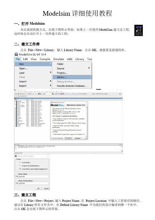
Modelsim详细使用教程一、打开Medelsim双击桌面快捷方式,出现下图所示界面,如果上一次使用ModelSim建立过工程,这时候会自动打开上一次所建立的工程;二、建立工作库点击File->New->Library,输入Library Name,点击OK,就能看见新建的库。
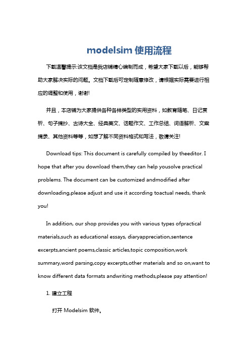
三、建立工程点击File->New->Project,输入Project Name,在Project Location 中输入工程保存的路径,建议在Library所在文件夹中。
在Default Library Name 中为我们的设计编译到哪一个库中。
点击OK会出现下图所示的界面。
四、为工程添加文件Create New File 为工程添加新建的文件;Add Existing File为工程添加已经存在的文件;Create Simulation为工程添加仿真;Create New Folder为工程添加新的目录。
这里我们点击Create New File,来写仿真代码。
输入File Name,再输入文件类型为Verilog (默认为VHDL,Modelsim也可以仿真System Verilog代码),Top Level表示文件在刚才所设定的工程路径下。
点击OK,并点击Close关闭Add items to the Project窗口。
这时候在Workspace窗口中出现了Project选项卡,里面有8_11.v,其状态栏有一个问号,表示未编译,双击该文件,这时候出现8_11.v的编辑窗口,可以输入我们的Verilog代码。
五、编写Verilog代码写完代码后,不能马上就编译,要先File->Save保存,否则,编译无效。
然后选择Compile->Compile All。
Transcript脚本窗口出现一行绿色字体Compile of 8_11.v was successful. 说明文件编译成功,并且该文件的状态栏显示绿色的对号。
modelsim教程

Secondary
– Units in the same library may use a common name – VHDL • Architectures • Package bodies – No Verilog secondary units
VHDL Predefined Libraries
Where
– – – – _primary.dat - encoded form of Verilog module or VHDL entity _primary.vhd - VHDL entity representation of Verilog ports <arch_name>.dat - encoded form of VHDL architecture verilog.asm and <arch_name>.asm - executable code files
ModelSim Design Units
Primary
– Must have a unique name in a given library – VHDL • Entities • Package Declarations • Configurations – Verilog • Modules • User Defined Primitives
Model Technology’s ModelSim
Main Window: Source Window:
Structure Window Wave & List Windows:
Process Window:
Signals & Variables Windows: Dataflow Window:
最好的Modelsim 6.0 入门

ModelSim入门(仅供内部使用)For internal use only拟制: Prepared by 黄超日期:Date2005-04-08审核: Reviewed by 日期:Dateyyyy-mm-dd审核: Reviewed by 日期:Dateyyyy-mm-dd批准: Granted by日期:Dateyyyy-mm-dd华为技术有限公司Huawei Technologies Co., Ltd.版权所有侵权必究All rights reserved修订记录Revision record目录Table of Contents1前言 (5)2逻辑仿真的必要性 (5)3仿真准备工作 (5)3.1库的新建与文件的编译 (5)3.2文件加载 (8)4仿真 (9)4.1wave窗口查看波形 (10)4.2其它仿真窗口 (12)5注意事项及小技巧 (12)5.1观察波形常用技巧 (13)5.2常用命令 (16)ModelSim入门关键词Key words:ModelSim 6.0、wave、仿真摘要Abstract:本文主要介绍ModelSim 6.0的使用。
缩略语清单List of abbreviations:1 前言本文以ModelSim 6.0为平台为大家介绍ModelSim的使用,旨在大家通过本文的学习能够对Modelsim仿真工具有较为全面的理解,并且能够使用该工具进行包括功能和时序仿真在内的逻辑验证。
本文面向的对象是刚涉及逻辑测试的工程师,文中对Modelsim仿真工具的使用和操作技巧作了详细的描述,大家可以按照文中的描述进行实例操作,将有助于熟悉Modelsim的操作运行过程。
2 逻辑仿真的必要性首先,通过逻辑仿真,能够及时发现并解决逻辑设计中遇到的绝大多数功能和时序问题,为后期逻辑的上板测试提供了良好保证。
其次,在上板测试中,由于环境所限,有些功能可能无法进行充分的验证,此时逻辑仿真可以作为上板测试很好的补充。
modelsim使用流程
modelsim使用流程下载温馨提示:该文档是我店铺精心编制而成,希望大家下载以后,能够帮助大家解决实际的问题。
文档下载后可定制随意修改,请根据实际需要进行相应的调整和使用,谢谢!并且,本店铺为大家提供各种各样类型的实用资料,如教育随笔、日记赏析、句子摘抄、古诗大全、经典美文、话题作文、工作总结、词语解析、文案摘录、其他资料等等,如想了解不同资料格式和写法,敬请关注!Download tips: This document is carefully compiled by theeditor. I hope that after you download them,they can help yousolve practical problems. The document can be customized andmodified after downloading,please adjust and use it according toactual needs, thank you!In addition, our shop provides you with various types ofpractical materials,such as educational essays, diaryappreciation,sentence excerpts,ancient poems,classic articles,topic composition,work summary,word parsing,copy excerpts,other materials and so on,want to know different data formats andwriting methods,please pay attention!1. 建立工程打开 Modelsim 软件。
选择“File”菜单,然后选择“New”->“Project”。
利用ModelSim SE6.0C实现时序仿真

1) 打开一个工程文件。
2) 打开Settings设置栏,选择EDA Tools Settings下的Simulation栏。
在右边出现的设置栏中将“Toolname”的下拉菜单选择“ModelSim(Verilog)”(如果工程用VHDL语言实现,则可以选择“ModelSim(VHDL)”;如果ModelSim使用的是for Altera的专用版本,则可以选择“ModelSim-Altera(Verilog)”或“ModelSim-Altera(VHDL)”)。
另外在设置栏中还有其他的核选框。
1. 如果选中“Maintain hierarchy”,则表示在做时序仿真时就能看到像在功能仿真的工程文件层次结构,可以找到定义的内部信号。
因为在做后仿时,源文件中的信号名称已经没有了,被映射为软件综合后自己生成的信号名,观察起来很不方便。
这个设置与ISE里综合右键属性的Keep Hierarchy选择YES的功能是一样的。
2. 如果选中“Generate netlist for functional simulation only”,则表示只能做功能仿真。
3) 点击“Start Compilation”按钮编译工程,完成之后在当前的工程目录下可以看到一个名为“Simulation”的新文件夹,下面的“ModelSim”文件夹下包括仿真需要的.vo网表文件和包含延迟信息的.sdo 文件。
4) 打开ModelSim软件(或者在Quartus下“Settings->EDA Tools Setting->Simulation”出现的设置栏中选中“Run this tool automatically after compilation”,直接从Quartus下调用ModelSim软件),可以在当前工程目录下新建一个Project。
在Project标签栏内点击右键,出现在快捷菜单中选择“Add toProject->Existing File…”。
Modelsim+se+6.0安装步骤、仿真步骤
设置输出网表文件的文件名、路径及格式等,一般情况下使用缺省值即可,如图4-12所示。点击完成后就关闭综合向导开始进行综合,在综合运行过程中,在信息窗口可看到滚动的综合结果及运行流程,出现本例中的pseudorandom.vhd的器件使用报告。如果信息窗口是关闭的,可点击Window\pseudorandom.vhd再次打开设计文件。在综合完成后信息窗口显示Finished Synthesis run。
现在可以尽情的享用。
LeonardoSpectrum是Mentor Graphics的子公司Exemplar Logic的专业VHDL/Verilog HDL综合软件,简单易用,可控性较强,可以在LeonardoSpectrum中综合优化并产生EDIF文件,作为QuartusII的编译输入,其运行界面如图4-6所示。该软件有三种逻辑综合方式:Synthesis Wizard(综合向导)、Quick Setup(快速完成)、Advanced FlowTabs(详细流程)方式。三种方式完成的功能基本相同,具体采用哪种方式可点击工具栏快捷图标或从Tools菜单中选择,如图4-7所示。Synthesis Wizard方式最简单,Advanced FlowTabs方式则最全面,该方式有六个选项单,分别完成以下功能:器件选择、设计文件输入、约束条件指定、优化选择、输出网表文件设置及选择调用布局布线工具。
图3-2模块编译
4仿真。首先是调用设计,选择Simulate>Simulate,出现如图3-3所示的对话框,选择该工程的testbench文件,出现如图3-4所示的窗口。单击右键,选择将所有信号(或你希望观察的信号)添加到wave窗口中,见图3-5所示。选择simulate>run>run all,如图3-6所示,出现图3-7中的波形。
modelsim安装+使用说明

1 Modelsim安装步骤此处以Modelsim Se v6.0的安装为例说明具体的安装步骤以及应该注意的事项:Modelsim Se v6.0的安装:运行Modelsim Se v6.0目录中的的自解压缩安装文件,如下图1-1所示:图1-1 自解压缩安装文件等待解压缩完成之后,会出现Modelsim Se v6.0的安装选择画面,如图1-2所示,图1-2 选择安装模式选择FULL Product 安装模式,出现如图3所示的安装界面,如图1-3所示图1-3选择next,然受选择yes,出现如图1-4所示的安装路径选择对话框,图1-4 选择安装路径这里我选择默认安装路径c:\Modeltech_6.0。
连续两次next出现如图1-5所示的文件安装界面图1-5安装文件复制完成后会弹出如图1-6所示的对话框图1-6 选择“是(Y)”出现图1-7图1-7 和图1-8图1-8 点击“确定”安装完成后,出现图1-9图1-9 点击“是(Y)”后在桌面建立快捷方式。
紧接着出现图1-10图1-10 添加桌面快捷方式选择默认。
图1-11 完成安装完成安装,如图1-11所示。
2 配置Modelsim Se v6.0的的环境变量:先找到的安装文件夹的crack目录下的keygen.exe文件,然后运行。
如图2-1所示:图2-1点击“Generate”会出现图2-2。
图2-2这表示License文件生成成功。
将生成的License文件license.dat复制到Modelsim Se v6.0安装目录(我这里的安装目录是C:\Modeltech_6.0)。
然后打开计算机属性对话框的“高级”选项卡,找到用户环境变量LM_LICENSE_FILE,然后编辑,输入变量值C:\Modeltech_6.0\license.dat(也就是License文件的物理路径)如图2-3所示:图2-3 Modelsim v6.0 用户环境变量设置编辑完成之后,确定。
modelsim教程

準備事項1.ModelSim試用版下載2.範例程式下載(史丹佛大學一門課的期末專題Implememtation of ViterbiDecoder:constrain length K=3, code rate R=1/2,register-exchange)整個project共含7個Verilog程式:system.v (top-level)|-- clkgen.v|-- chip_core.v|-- controller.v|-- spu.v|-- acs4.v|-- acs1.v(或是另外一個Verilog的簡單例子,可以從C:\ SynaptiCAD\ Examples\ TutorialFiles\VeriLoggerBasicVerilo gSimulation\ add4.v and add4test.v)(或是另外一個VHDL的簡單例子,可以從C:\ Modeltech_5.7e\ examples\ adder.vhd and testadder.vhd)ModelSim PE /LE /SE 差別在哪?本篇文章內容主要在教導軟體使用,以Verilog程式為範例。
假設各位讀者已經熟悉Verilog,廢話不多說,讓我們馬上來見識一下ModelSim ...快速上手四部曲:建立Project、引進HDL Files、Compile、模擬(Simulate/Loading and Run)1.建立一個新的Project1-1 第一次執行程式時,可以從[開始] \ [程式集] \ ModelSim SE \ ModelSim;或是執行ModelSim在桌面的捷徑在Library標籤頁中,展開各Library就可以看到其下含的所有Package (for VHDL),進一步以Edit打開,可檢視該Package與Package Body內容1-2File \ New \ Project ...輸入project name and Location按OK鍵後•指定的路徑下會產生一個叫"work"的預設子資料夾,還有Viterbi.cr.mti、Viterbi.mpf 兩個檔案•主操作畫面左邊的Workspace內,在原本的Library標籤外,會出現另一個Project標籤(但此時裡面內容是空的)•還會蹦出另一個"Add items.mpf 檔儲存的是此project的相關資料,下次要開啟此project 就是利用File \ Open \Project... 開啟此.mpf若要移除之前建立的project,請從File \ Delete \Project... 移除2.載入Project 的HDL source codes按"Add items to the Project"視窗中的"Add Existing File" (或是從File \ Add to Project \ Existing Files ...)HDL files擺放的位置,路徑名稱不能有中文,否則軟體會抓不到files關掉"Add items to the Project"視窗,此時的Project下出現了HDL File,一堆問號表示這些檔案都還沒compile。
仿真工具Modelsim的使用方法简述

仿真工具Modelsim的使用
Mentor公司的ModelSim是业界最优秀的HDL语言仿真软件,它能提供友好的仿真环境,是业界唯一的单内核支持VHDL和Verilog混合仿真的仿真器。
它采用直接优化的编译技术、Tcl/Tk技术、和单一内核仿真技术,编译仿真速度快,编译的代码与平台无关,便于保护IP核,个性化的图形界面和用户接口,为用户加快调错提供强有力的手段,是FPGA/ASIC设计的首选仿真软件。
使用 modelsim
打开 modelsim,选择菜单 file→new→project
创建工程文件夹和名称
然后点击OK.
然后创建一个新的文件夹.
创建文件名称选择文件类别,我们选择verilog. 然后双击工程窗口的文件或者右键选择“edit”之后编程并保存.
之后,右键点击文件选择compile列表
在状态窗口可以看见运行结果的错误或者报警。
如果结果顺利就可以编写测试程
序。
右键点击工程菜单并添加一个新的工程文件。
命名、编程和纠错。
如果编译所有文件是成功的就可以模拟这一工程。
单击project窗口附近的library。
然后再展开work工程。
右击hfad_test和模拟或者您可以点击模拟按钮
然后会看到一个simulate窗口在project窗口附近。
右击hfad_test,然后add → to wave → all items in region
将看到波行窗。
现在可以确定模拟时间和运行。
十六进制。
完成了一个工程。
modelsim后仿真教程

1.3.2后端仿真(1)在源代码窗口中选择【adder】模块,然后在相关的程序窗口【Process】中单击【Implement Design】左侧的“+”号展开程序组,单击【Place & Route】左侧的“+”号展开程序组,双击【Generate Post-Place & Route Simulation Model】,生成后端仿真所需要的文件,如图1-21所示,编译成功以后,如图1-22所示。
图1-21图1-22(1)双击桌面上的Modelsim SE6.0的快捷图标启动Modelsim 6.0SE仿真开发环境,或者从Windows XP操作系统中选择【开始】/【所有程序】/【Modelsim SE 6.0】/【Modelsim】命令启动Modelsim,如图1-23所示。
图1-23(2)新建后仿工程【adder】,如图1-24所示。
在【Project Name】一栏中输入工程名称【adder】,在【Project Location】中选择默认路径,如图1-25所示,单击,进入添加仿真文件页面,如图1-26所示。
图1-24图1-25图1-26(3)在图1-26中选择【Add Existing File】,进入文件添加页面,如图1-27所示。
单击【Copy to project directory】,将所需要添加的存在文件复制到仿真工程【adder】的文件夹下。
单击,选择需要添加的文件集。
后端仿真需要三个.v文件。
这三个文件分别是【test_adder.v】、【adder_timsim.v】、【glbl.v】,其中,【glbl.v】文件在Xilinx安装盘:\Xilinx\verilog\src文件夹里。
然后,打开【adder_timsim.v】文件,把sdf文件的相对路径netgen/par/adder_timesim.sdf改为绝对路径D:\program\XILINX10.1\ISE\study\adder\netgen\par,如图1-28所示。
modelsim使用方法
Using ModelSim to Simulate LogicCircuits for Altera FPGA Devices1IntroductionThis tutorial is a basic introduction to ModelSim,a Mentor Graphics’simulation tool for logic circuits.We show how to perform functional and timing simulations of logic circuits implemented by using Quartus II CAD software.The reader is expected to have the basic knowledge of Verilog hardware description language,and the Altera Quartus II CAD software.Contents:•Introduction to simulation•What is ModelSim?•Functional simulation using ModelSim•Timing simulation using ModelSim1 Altera Corporation-University ProgramSeptember20102BackgroundDesigners of digital systems are inevitably faced with the task of testing their designs.Each design can be composed of many modules,each of which has to be tested in isolation and then integrated into a design when it operates correctly.To verify that a design operates correctly we use simulation,which is a process of testing the design by applying inputs to a circuit and observing its behavior.The output of a simulation is a set of waveforms that show how a circuit behaves based on a given sequence of inputs.The generalflow of a simulation is shown in Figure1.Figure1.The simulationflow.There are two main types of simulation:functional and timing simulation.The functional simulation tests the logical operation of a circuit without accounting for delays in the circuit.Signals are propagated through the circuit using logic and wiring delays of zero.This simulation is fast and useful for checking the fundamental correctness of the designed circuit.The second step of the simulation process is the timing simulation.It is a more complex type of simulation,where logic components and wires take some time to respond to input stimuli.In addition to testing the logical operation of the circuit,it shows the timing of signals in the circuit.This type of simulation is more realistic than the functional simulation;however,it takes longer to perform.2Altera Corporation-University ProgramSeptember2010In this tutorial,we show how to simulate circuits using ModelSim.You need Quartus II CAD software and ModelSim software,or ModelSim-Altera software that comes with Quartus II,to work through the tutorial.3Example DesignOur example design is a serial adder.It takes8-bit inputs A and B and adds them in a serial fashion when the g o input is set to1.The result of the operation is stored in a9-bit sum register.A block diagram of the circuit is shown in Figure2.It consists of three shift registers,a full adder,aflip-flop to store carry-out signal from the full adder and afinite state machine(FSM).The shift registers A andB are loaded with the values of A and B.After the st ar t signal is set high,these registers are shifted right one bit at a time.At the same time the least-significant bits of A and B are added and the result is stored into the shift register sum.Once all bits of A and B have been added,the circuit stops and displays the sum until a new addition is requested.Figure2.Block diagram of a serial-adder circuit.The Verilog code for the top-level module of this design is shown in Figure3.It consists of the instances of the shift registers,an adder and afinite state machine(FSM)to control this design.3 Altera Corporation-University ProgramSeptember20101.module serial(A,B,start,resetn,clock,sum);2.input[7:0]A,B;3.input resetn,start,clock;4.output[8:0]LEDR;5.6.//Registers7.wire[7:0]A_reg,B_reg;8.wire[8:0]sum;9.reg cin;10.11.//Wires12.wire reset,enable,load;13.wire bit_sum,bit_carry;14.15.//Confrol FSM16.FSM my_control(start,clock,resetn,reset,enable,load);17.18.//Datapath19.shift_reg reg_A(clock,1’b0,A,1’b0,enable,load,A_reg);20.shift_reg reg_B(clock,1’b0,B,1’b0,enable,load,B_reg);21.22.//a full adder23.assign bit_carry,bit_sum=A_reg[0]+B_reg[0]+cin;24.25.always@(posedge clock)26.begin27.if(enable)28.if(reset)29.cin<=1’b0;30.else31.cin<=bit_carry;32.end33.34.shift_reg reg_sum(clock,reset,9’d0,bit_sum,enable,1’b0,sum);35.defparam reg_sum.n=9;36.endmoduleFigure3.Verilog code for the top-level module of the serial adder.The Verilog code for the FSM is shown in Figure4.The FSM is a3-state Mealyfinite state machine,where thefirst and the third state waits for the st ar t input to be set to1or0,respectively.The computation of the sum of A and B4Altera Corporation-University ProgramSeptember2010happens during the second state,called WORK_STATE.The FSM completes computation when the counter reachesa value of8,indicating that inputs A and B have been added.The state diagram for the FSM is shown in Figure5.1.module FSM(start,clock,resetn,reset,enable,load);2.parameter WAIT_STATE=2’b00,WORK_STATE=2’b01,END_STATE=2’b11;3.input start,clock,resetn;4.output reset,enable,load;5.6.reg[1:0]current_state,next_state;7.reg[3:0]counter;8.9.//next state logic10.always@(*)11.begin12.case(current_state)13.WAIT_STATE:14.if(start)next_state<=WORK_STATE;15.else next_state<=W AIT_STATE;16.WORK_STATE:17.if(counter==4’d8)next_state<=END_STATE;18.else next_state<=WORK_STATE;19.END_STATE:20.if(∼start)next_state<=W AIT_STATE;21.else next_state<=END_STATE;22.default:next_state<=2’bxx;23.endcase24.end25.26.//state registers and a counter27.always@(posedge clock or negedge resetn)28.begin29.if(∼resetn)30.begin31.current_state<=W AIT_STATE;32.counter=’d0;33.end34.else35.beginFigure4.Verilog code for the FSM to control the serial adder(Part a).5 Altera Corporation-University ProgramSeptember201036.current_state<=next_state;37.if(current_state==W AIT_STATE)38.counter<=’d0;39.else if(current_state==WORK_STATE)40.counter<=counter+1’b1;41.end42.end43.//Outputs44.assign reset=(current_state==WAIT_STATE)&start;45.assign load=(current_state==W AIT_STATE)&start;46.assign enable=load|(current_state==WORK_STATE);47.endmoduleFigure4.Verilog code for the FSM to control the serial adder(Part b).Figure5.State diagram.The Verilog code for the shift register is given in Figure6.It consists of synchronous control signals to allow data to be loaded into the shift register,or reset to0.When enable input is set to1and the data is not being loaded or reset, the contents of the shift register are moved one bit to the right(towards the least-significant bit).6Altera Corporation-University ProgramSeptember20101.module shift_reg(clock,reset,data,bit_in,enable,load,q);2.parameter n=8;3.4.input clock,reset,bit_in,enable,load;5.input[n-1:0]data;6.output reg[n-1:0]q;7.8.always@(posedge clock)9.begin10.if(enable)11.if(reset)12.q<=’d0;13.else14.begin15.if(load)16.q<=data;17.else18.begin19.q[n-2:0]<=q[n-1:1];20.q[n-1]<=bit_in;21.end22.end23.end24.endmoduleFigure6.Verilog code for the shift register.The design is located in the example/functional and example/timing subdirectories provided with this tutorial.A Quartus II project for this design has been created as well.In the following sections,we use the serial adder example to demonstrate how to perform simulation using Mod-elSim.We begin by describing a procedure to perform a functional simulation,and then discuss how to perform a timing simulation.4Functional Simulation with ModelSimWe begin this tutorial by showing how to perform a functional simulation of the example design.We start by opening the ModelSim program.7 Altera Corporation-University ProgramSeptember2010Figure7.ModelSim window.The ModelSim program window,shown in Figure7,consists of four sections:the main menu at the top,a set of workspace tabs on the left,a work area on the right,and a command prompt at the bottom.The menu is used to access functions available in ModelSim.The workspace contains a list of modules and libraries of modules available to you,as well as details of the project you are working on.The work area on the right is the space where windows containing waveforms and/or textfiles will be displayed.Finally,the command prompt at the bottom shows feedback from the simulation tool and allows users to enter commands.To perform simulation with ModelSim follow a basicflow shown in Figure1.We begin by creating a project where all designfiles to be simulated are included.We compile the design and then run the simulation.Based on the results of the simulation,the design can be altered until it meets the desired specifications.4.1Creating a ProjectTo create a project in ModelSim,select New>Project...from the File menu.A create project window shown in Figure8will appear.8Altera Corporation-University ProgramSeptember2010Figure8.Creating a new project.The create project window consists of severalfields:project name,project location,default library name,and copy settingsfield.Project name is a user selected name and the location is the directory where the sourcefiles are located.For our example,we choose the project name to be serial,to match the top-level module name of our example design,and the location of the project is the example/functional subdirectory.The default library namefield specifies a name by which ModelSim catalogues designs.For example,a set offiles that describe the logical behaviour of components in an Altera Cyclone II device are stored in the cycloneii library. This allows the simulator to include a set offiles in simulation as libraries rather than individualfiles,which is particularly useful for timing simulations where device-specific data is required.For the purpose of this tutorial, specify tutorial as the library name for your project.The lastfield in the create project window is the copy settingsfield.This allows default settings to be copied from the initializationfile and applied to your project.Now,click OK to proceed to addfiles to the project using the window shown in Figure9.Altera Corporation-University Program September20109Figure9.Add afile to project window.The window in Figure9gives several options to addfiles to the project,including creating newfiles and directories, or adding existingfiles.Since thefile for this tutorial exists,click Add Existing File and select serial.vfile.Once thefile is added to the project,it will appear in the Project tab on the left-hand side of the screen,as shown in Figure10.Figure10.Workspace window after the project is created.Now that all designfiles have been included in the project,click Close to close the window in Figure9.10Altera Corporation-University ProgramSeptember20104.2Compiling a ProjectOnce the project has been created,it is necessary to compile pilation in ModelSim checks if the project files are correct and creates intermediate data that will be used during simulation.To perform compilation,select Compile All from the Compile menu.When the compilation is successful,a green check mark will appear to the right of the serial.vfile in the Project tab.4.3SimulationTo begin a simulation of the design,the software needs to be put in simulation mode.To do this,select Start Simulation...from the Simulate menu.The window in Figure11will appear.Figure11.Start simulation mode in ModelSim.The window to start simulation consists of many tabs.These include a Design tab that lists designs available for simulation,VHDL and Verilog tabs to specify language specific options,a Library tab to include any additional libraries,and timing and other options in the remaining two tabs.For the purposes of the functional simulation,we only need to look at the Design tab.In the Design tab you will see a list of libraries and modules you can simulate.In this tutorial,we want to simulate a module called serial,described in serial.vfile.To select this module,scroll down and locate the tutorial library and click on the plus(+)sign.You will see three modules available for simulation:FSM,serial,and shift_reg.Select the serial module,as shown in Figure11and click OK to begin simulation.When you click OK,ModelSim will begin loading the selected libraries and preparing to simulate the circuit.For the example in this tutorial,the preparation should complete quickly.Once ModelSim is ready to simulate your design, you will notice that several new tabs on the left-hand side of the screen and a new Objects window have appeared, as shown in Figure12.Figure12.New displays in the simulation mode.A key new tab on the left-hand side is the sim tab.It contains a hierarchical display of design units in your circuit in a form of a table.The columns of the table include the instance name,design unit and design unit type names. The rows of the table take a form of an expandable tree.The tree is rooted in the top-level entity called serial.Each module instance has a plus(+)sign next to its name to indicate it can be expanded to allow users to examine the contents of that module instance.Expanding the top-level entity in this view gives a list of modules and/or constructs within it.For example,in Figure12the top-level entity serial is shown to contain an instance of the FSM module,called my_control,three instances of a shift_reg module,four assign statements and an always block.Double-clicking on any of the constructs will cause ModelSim to open a sourcefile and locate the given construct within it.Double-clicking on a module instance will open a sourcefile and point to the description of the module in the sourcefile.In addition to showing modules and/or constructs,the sim tab can be used to locate signals for simulation.Notice that when the serial module is highlighted,a list of signals(inputs,outputs and local wires)is shown in the Objects window.The signals are displayed as a table with four columns:name,value,kind and mode.The name of a signal may be preceded by a plus(+)sign to indicate that it is a bus.The top-level entity comprises signals A,B,resetn, start,and clock as inputs,a sum output and a number of internal signals.12Altera Corporation-University ProgramWe can also locate signals inside of module instances in the design.To do this,highlight a module whose signals you wish to see in the Objects window.For example,to see the signals in the my_control instance of the FSM module, highlight the my_control instance in the sim tab.This will give a list of signals inside of the instance as shown in Figure13.Figure13.Expanded my_control instance.Using the sim tab and the Objects window we can select signals for simulation.To add a signal to simulation, right-click on the signal name in the Objects window and select Add>T o Wave>Selected items from the pop-up ing this method,add signals A,B,clock,resetn,start,sum,and current_state to the simulation.When you do so,a waveform window will appear in the work area.Once you have added these signals to the simulation, press the Undock button in the top-right corner of the waveform window to make it a separate window,as shown in Figure14.Figure14.A simulation window.Before we begin simulating the circuit,there is one more useful feature worth noting.It is the ability to combine signals and create aliases.It is useful when signals of interest are not named as well as they should be,or the given names are inconvenient for the purposes of simulation.In this example,we rename the start signal to go by highlighting the start signal and selecting Combine Signals...from the Tools menu.The window in Figure15will appear.14Altera Corporation-University Programbine signals window.In the textfield labeled Result name type go and press the OK button.This will cause a new signal to appear in the simulation window.It will be named go,but it will have an orange diamond next to its name to indicate that it is an alias.Once the go alias is created,the original start input is no longer needed in the simulation window,so removeit by highlighting it and pressing the delete key.Your simulation window should now look as in Figure16.Figure16.Simulation window with aliased signals.Now that we set up a set of signals to observe we can begin simulating the circuit.There are two ways to run a simulation in ModelSim:manually or by using scripts.A manual simulation allows users to apply inputs and advance the simulation time to see the results of the simulation in a step-by-step fashion.A scripted simulation allows the user to create a script where the sequence of input stimuli are defined in afile.ModelSim can read thefile and apply input stimuli to appropriate signals and then run the simulation from beginning to end,displaying results only when the simulation is completed.In this tutorial,we perform the simulation manually.In this simulation,we use a clock with a100ps period.At every negative edge of the clock we assign new values to circuit inputs to see how the circuit behaves.To set the clock period,right-click on the clock signal and select Clock...from the pop-up menu.In the window that appears,set the clock period to100ps and thefirst edge to be the falling edge,as shown in Figure17.Then click OK.16Altera Corporation-University ProgramFigure17.Set the clock period.We begin the simulation be resetting the circuit.To reset the circuit,set the resetn signal low by right-clicking on it and selecting the Force...option from the pop-up menu.In the window that appears,set Value to0and click OK. In a similar manner,set the value of the go signal to0.Now that the initial values for some of the signals are set,wecan perform thefirst step of the simulation.To do this,locate the toolbar buttons shown in Figure18.The toolbar buttons shown in Figure18are used to step through the simulation.The left-most button is the restartbutton,which causes the simulation window to be cleared and the simulation to be restarted.The textfield,shownwith a100ps string inside it,defines the amount of time that the simulation should run for when the Run button(tothe right of the textfield)is pressed.The remaining three buttons,Continue,Run-All and Break,can be used toresume,start and interrupt a simulation,respectively.We will not need them in this tutorial.To run a simulation for100ps,set the value in the textfield to100ps and press the Run button.After the simulationrun for100ps completes,you will see the state of the circuit as shown in Figure19.Figure19.Simulation results after100ps.In thefigure,each signal has a logic state.Thefirst two signals,A and B,are assigned a value between0and1in a blue color.This value indicates high impedance,and means that these signals are not driven to any logic state.The go and resetn signals is at a logic0value thereby resetting the circuit.The clock signal toggles state every50ps, starting with a falling edge at time0,a rising edge at time50ps and another falling edge at100ps.Now that the circuit is reset,we can begin testing to see if it operates correctly for desired inputs.To test the serial adder we will add numbers143and57,which should result in a sum of200.We can set A and B to143and57, respectively,using decimal notation.To specify a value for A in decimal,right-click on it,and choose Force... from the pop-up menu.Then,in the Valuefield put10#143.The10#prefix indicates that the value that follows is specified in decimal.Similarly,set the value of input_B to57.To see the decimal,rather than binary,values of buses in the waveform window we need to change the Radix of A and B to unsigned.To change the radix of these signals,highlight them in the simulation window and select Radix >Unsigned from the Format menu,as shown in Figure20.Change the radix of the sum signal to unsigned as well.18Altera Corporation-University ProgramFigure20.Changing the radix of A,B and sum signals.Now that inputs A and B are specified,set resetn to1to stop the circuit from resetting.Then set go to1to begin serial addition,and press the Run button to run the simulation for another100ps.The output should be as illustrated in Figure21.Notice that the values of inputs A and B are shown in decimal as is the sum.The circuit also recognizeda go signal and moved to state01to begin computing the sum of the two inputs.Figure21.Simulation results after200ps.To complete the operation,the circuit will require9clock cycles.To fast forward the simulation to see the result,specify900ps in the textfield next to the run button,and press the run button.This brings the simulation to time1100ps,at which point a result of summation is shown on the sum signal,as illustrated in Figure22.Figure22.Simulation results after1100ps.We can see that the result is correct and thefinite state machine controlling the serial adder entered state11,in which it awaits the go signal to become0.Once we set the go signal to0and advance the simulation by100ps,the circuit will enter state00and await a new set of inputs for addition.The simulation result after1200ps is shown inFigure23.Figure23.Simulation results after1200ps.At this point,we can begin the simulation for a new set of inputs as needed,repeating the steps described above.Wecan also restart the simulation by pressing the restart button to begin again from time0.By using the functional simulation we have shown that the serial.vfile contains an accurate Verilog HDL description20Altera Corporation-University Programof a serial adder.However,this simulation did not verify if the circuit implemented on an FPGA is correct.This is because we did not use a synthesized,placed and routed circuit as input to the simulator.The correctness of the implementation,including timing constraints can be verified using timing simulation.5Timing Simulation with ModelSimTiming simulation is an enhanced simulation,where the logical functionality of a design is tested in the presence of delays.Any change in logic state of a wire will take as much time as it would on a real device.This forces the inputs to the simulation be realistic not only in terms of input values and the sequence of inputs,but also the time when the inputs are applied to the circuit.For example,in the previous section we simulated the sample design and used a clock period of100ps.This clock period is shorter than the minimum clock period for this design,and hence the timing simulation would fail to produce the correct result.To obtain the correct result,we have to account for delays when running the simulation and use a clock frequency for which the circuit operates correctly.For Altera FPGA-based designs the delay information is available after the design is synthesized,placed and routed, and is generated by Quartus II CAD software.The project for this part of the tutorial has been created for you in the example/timing subdirectory.5.1Setting up a Quartus II Project for Timing Simulation with ModelSimTo perform timing simulation we need to set up Quartus II software to generate the necessary delay information for ModelSim by setting up EDA Tools for simulation in the Quartus II project.To set up EDA Tools for simulation, open the Quartus II project in example/timing subdirectory,and select Settings...from the Assignments menu.A window shown in Figure24will appear.The window in thefigure consists of a list on the left-hand side to select the settings category and a window area on the right-hand side that displays the settings for a given category.Select Simulation from the EDA Tool Settings category to see the screen shown on the right-hand side of Figure24.The right-hand side of thefigure contains the tool name at the top,EDA Netlist Writer settings in the middle,and NativeLink settings at the bottom.The tool name is a drop-down list containing the names of simulation tools for which Quartus II can produce a netlist with timing information automatically.This list contains many well-known simulation tools,including ModelSim.From the drop-down list select ModelSim-Altera.Once a simulation tool is selected,EDA Netlist Writer settings become available.These settings configure Quartus II to produce input for the simulation tool.Quartus II will use these parameters to describe an implemented design using a given HDL language,and annotate it with delay information obtained after compilation.The settings we can define are the HDL language,simulation time scale that defines time step size for the simulator to use,the location where the writer saves design and delay information,and others.For the purpose of this tutorial,only thefirst three settings are used.Set these settings to match those shown in Figure24and click OK.With the EDA Tools Settings specified,we can proceed to compile the project in Quartus II.The compilation process synthesizes,places,and routes the design,and performs timing analysis.Then it stores the compilation result in theFigure24.Quartus II EDA simulation tool settings.simulation directory for ModelSim to use.Take a moment to examine thefiles generated for simulation using a text editor.The two mainfiles are serial.vo,and serial_v.sdo.The serial.vofile is a Verilogfile for the design.Thefile looks close to the original Verilogfile,except that the design now contains a wide array of modules with a cycloneii_prefix.These modules describe resources on an Altera Cyclone II FPGA,on which the design was implemented using lookup tables,flip-flops,wires and I/O ports. The list delays for each module instance in the design is described in the serial_v.sdofile.22Altera Corporation-University Program5.2Running a Timing SimulationTo simulate the design using timing simulation we must create a ModelSim project.The steps are the same as in the previous section;however,the project is located in the example/timing/simulation/modelsim subdirectory,and the sourcefile is serial.vo.We do not need to include the serial_v.sdofile in the project,because a reference to it is included in the serial.vofile.Once you added the sourcefile to the project,compile it by selecting Compile All from the Compile menu.The next step in the simulation procedure is to place the ModelSim software in simulation mode.In the previous section,we did this by selecting Start Simulation...from the Simulate menu,and specifying the project name. To run a timing simulation there is an additional step required to include the Altera Cyclone II device library in the simulation.This library contains information about the logical operation of modules with cycloneii_prefix.To include the Cyclone II library in the project,select Start Simulation...from the Simulate menu and select the Library tab as shown in Figure25.Figure25.Including Altera Cyclone II library in ModelSim project.The Altera Cyclone II library is located in the altera/verilog/cycloneii directory in the ModelSim-Altera software. To add this library to your project,include the altera/verilog/cycloneii directory using the Add...button.Then,clickon the Design tab,select your project for simulation,and click OK.When the ModelSim software enters simulation mode,you will see a significant difference in the contents of the workspace tabs on the left-hand side of the window as compared to when you ran the functional simulation.In particular,notice the sim tab and the Objects window shown in Figure26.The list of modules in the sim tab is larger,and the objects window contains more signals.This is due to the fact that the design is constructed using components on an FPGA and is more detailed in comparison to an abstract description we used in the previous section of the tutorial.Figure26.Workspace tabs and Objects window for timing simulation.We simulate the circuit by creating a waveform that includes signals A,B,go,and resetn aliases as before.In addition,we include the clock,reg_sum|q,reg_A|q,and reg_B|q signals from the Objects window.Signals reg_A|q and reg_B|q are registers that store A and B at the positive edge of the clock.The reg_sum|q signal is a register that stores the resulting sum.Begin the simulation by resetting the circuit.To do this,set go and resetn signals to0.Also,set the clock input to have a period of20ns,whosefirst edge is a falling edge.To run the simulation,set the simulation step to20ns and press the Run button.The simulation result is shown in Figure27.24Altera Corporation-University Program。
- 1、下载文档前请自行甄别文档内容的完整性,平台不提供额外的编辑、内容补充、找答案等附加服务。
- 2、"仅部分预览"的文档,不可在线预览部分如存在完整性等问题,可反馈申请退款(可完整预览的文档不适用该条件!)。
- 3、如文档侵犯您的权益,请联系客服反馈,我们会尽快为您处理(人工客服工作时间:9:00-18:30)。
Modelsim 6.0 使用教程1. Modelsim简介Modelsim仿真工具是Model公司开发的。
它支持Verilog、VHDL以及他们的混合仿真,它可以将整个程序分步执行,使设计者直接看到他的程序下一步要执行的语句,而且在程序执行的任何步骤任何时刻都可以查看任意变量的当前值,可以在Dataflow窗口查看某一单元或模块的输入输出的连续变化等,比quartus自带的仿真器功能强大的多,是目前业界最通用的仿真器之一。
对于初学者,modelsim自带的教程是一个很好的选择,在Help->SE PDF Documentation->Tutorial里面.它从简单到复杂、从低级到高级详细地讲述了modelsim的各项功能的使用,简单易懂。
但是它也有缺点,就是它里面所有事例的初期准备工作都已经放在example文件夹里,直接将它们添加到modelsim就可以用,它假设使用者对当前操作的前期准备工作都已经很熟悉,所以初学者往往不知道如何做当前操作的前期准备。
2.安装同许多其他软件一样,Modelsim SE同样需要合法的License,通常我们用Kengen产生license.dat。
⑴.解压安装工具包开始安装,安装时选择Full product安装。
当出现InstallHardware Security Key Driver时选择否。
当出现Add Modelsim To Path选择是。
出现Modelsim License Wizard时选择Close。
⑵.在C盘根目录新建一个文件夹flexlm,用Keygen产生一个License.dat,然后复制到该文件夹下。
⑶.修改系统的环境变量。
右键点击桌面我的电脑图标,属性->高级->环境变量->(系统变量)新建。
按下图所示内容填写,变量值内如果已经有别的路径了,请用“;”将其与要填的路径分开。
LM_LICENSE_FILE = c:\flexlm\license.dat⑷.安装完毕,可以运行。
3. Modelsim仿真方法Modelsim的仿真分为前仿真和后仿真,下面先具体介绍一下两者的区别。
3.1 前仿真前仿真也称为功能仿真,主旨在于验证电路的功能是否符合设计要求,其特点是不考虑电路门延迟与线延迟,主要是验证电路与理想情况是否一致。
可综合FPGA代码是用RTL级代码语言描述的,其输入为RTL级代码与Testbench.3.2 后仿真后仿真也称为时序仿真或者布局布线后仿真,是指电路已经映射到特定的工艺环境以后,综合考虑电路的路径延迟与门延迟的影响,验证电路能否在一定时序条件下满足设计构想的过程,是否存在时序违规。
其输入文件为从布局布线结果中抽象出来的门级网表、Testbench和扩展名为SDO或SDF的标准时延文件。
SDO或SDF的标准时延文件不仅包含门延迟,还包括实际布线延迟,能较好地反映芯片的实际工作情况。
一般来说后仿真是必选的,检查设计时序与实际的FPGA运行情况是否一致,确保设计的可靠性和稳定性。
3.3 Modelsim仿真的基本步骤Modelsim的仿真主要有以下几个步骤:建立库并映射库到物理目录;编译原代码(包括Testbench;执行仿真。
3.3.1 建立库在执行一个仿真前先建立一个单独的文件夹,后面的操作都在此文件下进行,以防止文件间的误操作。
然后启动Modelsim将当前路径修改到该文件夹下,修改的方法是点File->Change Directory选择刚刚新建的文件夹见下图。
仿真库是存储已编译设计单元的目录,modelsim中有两类仿真库,一种是工作库,默认的库名为work,另一种是资源库。
Work库下包含当前工程下所有已经编译过的文件。
所以编译前一定要建一个work库,而且只能建一个work库。
资源库存放work库中已经编译文件所要调用的资源,这样的资源可能有很多,它们被放在不同的资源库内。
例如想要对综合在cyclone芯片中的设计做后仿真,就需要有一个名为cyclone_ver的资源库。
映射库用于将已经预编译好的文件所在的目录映射为一个modelsim可识别的库,库内的文件应该是已经编译过的,在Workspace窗口内展开该库应该能看见这些文件,如果是没有编译过的文件在库内是看不见的。
建立仿真库的方法有两种。
一种是在用户界面模式下,点File->New->Library出现下面的对话框,选择a new library and a logical mapping to it,在Library Name内输入要创建库的名称,然后OK,即可生成一个已经映射的新库。
另一种方法是在Transcript窗口输入以下命令:vlib work/* 库名 */vmap work work/* 映射的逻辑名称 存放的物理路径 */ 如果要删除某库,只需选中该库名,点右键选择Delete即可。
需要注意的是不要在modelsim外部的系统盘内手动创建库或者添加文件到库里;也不要modelsim用到的路径名或文件名中使用汉字,因为modelsim可能无法识别汉字而导致莫名其妙的错误。
3.3.2 编写与编译测试文件在编写Testbench之前最好先将要仿真的目标文件编译到工作库中,点Compile->Compile或,将出现下面的对话框,在Library中选择工作库,在查找范围内找到要仿真的目标文件,然后点Compile和Done。
或在命令行输入vlog fulladder.v。
此时目标文件已经编译到工作库中,在Library中展开工作库会发现该文件。
当对要仿真的目标文件进行仿真时需要给文件中的各个输入变量提供激励源,并对输入波形进行的严格定义,这种对激励源定义的文件称为Testbench,即测试台文件。
下面先讲一下Testbench的产生方法。
我们可以在modelsim内直接编写Testbench,而且modelsim还提供了常用的各种模板。
具体步骤如下:⑴.执行File->New->Source->verilog,或者直接点击工具栏上的新建图标,会出现一个verilog文档编辑页面,在此文档内设计者即可编辑测试台文件。
需要说明的是在Quartus中许多不可综合的语句在此处都可以使用,而且testbench只是一个激励源产生文件,只要对输入波形进行定义以及显示一些必要信息即可,切记不要编的过于复杂,以免喧宾夺主。
⑵.Modelsim提供了很多Testbench模板,我们直接拿过来用可以减少工作量。
点View->Source->Show Language Templates然后会出现一个加载工程,接着你会发现在刚才的文档编辑窗口左边出现了一个Language Templates窗口,见下图。
展开Verilog项,双击Creat Testbench会出现一个创建向导,见下图。
选择Specify Design Unit工作库下的目标文件,点Next,出现下面对话框可以指定Testbench的名称以及要编译到的库等,此处我们使用默认设置直接点Finish。
这时在Testbench内会出现对目标文件的各个端口的定义还有调用函数接下来,设计者可以自己往Testbench内添加内容了,然后保存为.v格式即可。
按照前面的方法把Testbench文件也编译到工作库中。
3.3.3 执行仿真因为仿真分为前仿真和后仿真,下面分别说明如何操作。
⑴.前仿真前仿真,相对来说是比较简单的。
在上一步我们已经把需要的文件编译到工作库内了,现在我们只需点simulate->Start Simulation或快捷按钮会出现start simulate对话框。
点击Design标签选择Work库下的Testbench文件,然后点OK即可,也可以直接双击Testbench文件,此时会出现下面的界面。
在主界面中会多出来一个Objects窗口,里面显示Testbench里定义的所有信号引脚,在Workspace里也会多出来一个Sim标签。
右键点击fuladder_tb.v,选择Add->Add to Wave,如下图所示。
然后将出现Wave窗口,现在就可以仿真了,见下图。
形也将继续延伸,见下图.若点,则仿真一直执行,直到点才停止仿真。
也可以在命令行输入命令:run @1000则执行仿真到1000ns,后面的1000也可以是别的数值,设计者可以修改。
在下一次运行次命令时将接着当前的波形继续往后仿真。
对于复杂的设计文件,最好是自己编写testbench文件,这样可以精确定义各信号以及各个信号之间的依赖关系等,提高仿真效率。
对于一些简单的设计文件,也可以在波形窗口自己创建输入波形进行仿真。
具体方法是双击work库里的目标仿真文件fulladder.v,然后点workspace窗口中出现的sim标签,右键点击fuladder,选择Add->Add to Wave,如下图所示。
然后将出现Wave窗口。
在wave窗口中选中要创建波形的信号,如此例中的a,然后右键点击,选择Create/Modify/Wave项出现下面的窗口,在Patterns中选择输入波形的类型,然后分别在右边的窗口中设定起始时间、终止时间以及单位,再点Next出现下面的窗口,我们把初始值的HiZ改为0,然后修改时钟周期和占空比,然后点Finish.接着继续添加其他输入波形,出现下面的结果。
前面出现的红点表示该波形是可编辑的。
后面的操作与用testbench文本仿真的方法相同如果设计者只想查看指定信号的波形,可以先选中objects窗口中要观察的信号,然后点右键选择Add to Wave->Selected signals,见下图,那么在Wave窗口中只添加选中的信号。
如果要保存波形窗口当前信号的分配,可以点File->Save->Format,在出现的对话框中设置保存路径及文件名,保存的格式为.do文件。
如果是想导出自己创建的波形(在文章最后有详细的解释)可以选择File->Export Waveform在出现的对话框中选择EVCD File并进行相关设置即可,如果导入设计的波形选择File->Import ECVD即可。
在主界面中点View->Debug Windows->Dataflow可以看到会出现dataflow窗口,在objects窗口中拖一个信号到该窗口中,你会发现在dataflow窗口中出现你刚才选中信号所在的模块,如果双击模块的某一引脚,会出现与该引脚相连的别的模块或者引线,见下图。
在dataflow窗口中点View->Show Wave,会在dataflow窗口中出现一个wave窗口,双击上面窗口中的某一模块,则在下面的wave窗口中出现与该模块相连的所有信号,如果已经执行过仿真,在wave窗口中还会出现对应的波形,见下图。