CX8502 车载车充芯片
瑞萨电子 CXD5602 用户手册说明书

CXD5602 User ManualContentsContents (2)Figure Contents (7)Table Contents (14)1Introduction (40)1.1Introduction (40)1.2Notation (40)1.2.1Notation of numerical value (40)2CXD5602 Outline (42)2.1Introduction (42)2.2Features (42)2.3Block Diagram (45)2.4Architecture Overview (46)2.5CPU Processor (47)2.5.1Application Processor (47)2.5.2System and I/O Processor (47)2.6Memory Mapping (49)2.6.1Memory Map of Each Block (50)2.6.2Main Memory (51)2.6.3System Memory (52)2.6.4Backup Memory (52)2.7Clock and Reset (52)2.7.1Overview (52)2.7.2Clock Architecture (55)2.8Power Management (57)2.8.1Overview (57)2.8.2Power Domain (57)2.8.3Power Supply States (60)3Function Details (62)3.1I/O Configuration (62)3.1.1Outline (62)3.1.2Function List (62)3.1.3Switching between HOST I/F Select Function and SWD Function (63)3.1.4Pin Multiplexer (64)3.2General Purpose Input/Output (GPIO) (95)3.2.1Outlines and Features (95)3.2.2Function List (95)3.2.3Function Specification Outlines (96)3.2.4Detailed Function and Control Specification (98)3.3Interrupt (121)3.3.1Overview and Features (121)3.3.2Register Descriptions (122)3.4PMU (Power Management Unit) (125)3.4.1Features and Overview (125)3.4.2Register List (135)3.4.3Register Descriptions (137)3.4.4Power Supply Control Flow (149)3.4.5Power Supply Control Example (163)3.5Clock and Reset (Clock Reset Generator) (167)3.5.1Overview (167)3.5.2Clock Scheme for CRG (167)3.5.3Analog Circuits (169)3.5.4Clock Setting Confirmation (172)3.5.5Power Domain Reset (175)3.5.6Reset by WDT (176)3.6RTC (179)3.6.1Outlines and Features (179)3.6.2Clock Input (180)3.6.3Function List (181)3.6.4Function Block Diagrams (181)3.6.5Detailed Function and Control Specification (184)3.7I2C (222)3.7.1Overview (222)3.7.2Features (225)3.7.3Functional description (226)3.7.4List of Registers (250)3.8DMAC (278)3.8.1Overview and Features (278)3.8.2Function Descriptions (278)3.8.3SDMAC (280)3.8.4HDMAC (283)3.8.5SYDMAC (285)3.8.6SYSUBDMAC (286)3.8.7ADMAC (287)3.8.8IDMAC (289)3.9SCU (Sensor Control Unit) (301)3.9.1SCU Overview and Features (301)3.9.2SCU Block Diagram (303)3.9.3Memory Map (304)3.9.4Clock Control (307)3.9.5Power Supply Control (313)3.9.6Interrupt (313)3.9.7MATH_PROC processing (318)3.9.8FIFO (328)3.9.9Sequencers (334)3.9.10DMA (356)3.9.11PWM (358)3.9.12SCU Register Details (369)3.9.13SCU Control Sequence (870)3.9.14Error Handling (914)3.9.15Restrictions (915)3.10SPI (930)3.10.1Overview and Features (930)3.10.2SPI0 (932)3.10.3SPI3 (933)3.10.4SPI4 (934)3.10.5SPI5 (936)3.10.6List of Registers (937)3.11UART (949)3.11.1Overview and Features (949)3.11.2UART1 (950)3.11.3UART2 (952)3.11.4List of Registers (953)3.12GNSS (965)3.13APP (967)3.13.1Function Overview (967)3.13.2Power Supply Control (970)3.13.3Clock Reset Control (971)3.13.4Description of APP_DSP Function (982)3.14SYSIOP Clock and Reset Control (1007)3.14.1Function Overiew (1007)3.14.2Power Supply Control (1010)3.14.3Clock and Reset Control (1011)3.15Audio Codec (1029)3.15.1Audio Codec Overview and Features (1029)3.15.2Audio Codec Block Diagram (1030)3.15.3Clock Supply (1035)3.15.4Standalone Operation (without the CXD5247) (1035)3.15.5External Interfaces (1036)3.15.6Details of Audio Codec Control Registers (1038)3.15.7Status Register (1083)3.15.8Interrupt Flag (1087)3.15.9Audio Codec Control Register List (1090)3.15.10Control Sequence (1106)3.16SDIO (1112)3.17eMMC (1112)3.18USB (1112)3.18.1Overview (1113)3.18.2Configuration Parameters (1118)3.18.3Theory of Operation (1124)3.18.4DMA Mode (1124)3.18.5Slave-Only Mode (1128)3.18.6Control and Status Registers (1131)3.18.7Slave-Only Operation (1172)3.18.8DMA Operation (1181)3.18.9Application Bus Protocol (Slave-Only Mode) (1201)3.18.10Application Bus Protocol (DMA Mode) (1203)3.18.11Software Implementation Guidelines (1205)3.18.12USB Programming (1211)3.18.13Multiple RxFIFO Controllers (1233)3.19CIS I/F (1238)3.202D Graphics (1238)3.21ADC (1239)3.21.1ADC Overview (1239)3.21.2ADC Block Diagram (1240)3.21.3Memory Map (1240)3.21.4Power Supply Control (1241)3.21.5Clock Control (1242)3.21.6Reset Control (1245)3.21.7Interrupt (1245)3.21.8FIFO writing Process (1245)3.21.9Gain Control (1246)3.21.10Performance Estimation (1248)3.21.11Synchronization Function with PWM (1249)3.21.12ADC Control Register Details (1249)3.21.13ADC Control Sequence (1285)3.21.14Restrictions (1285)3.21.15Error Handling (1286)4Appendix (1287)4.1Words and Terms (1287)4.1.1Words and Terms Used in This User Manual (1287)4.2Reference (1289)Revision History (1290)Figure ContentsFigure Block Diagram-1 CXD5602 Block Diagram (45)Figure Memory Mapping-2 Memory Map of the SYSIOP, GNSS, and APP (49)Figure Clock and Reset-3 Clock Diagram (56)Figure Power Management-4 Power Domain Layers (57)Figure Power Management-5 CXD5602 Power Domain (58)Figure Power Management-6 Changes of Power Supply States (61)Figure I/O Configuration-7 Switching between HOST I/F Function and SWD Function (63)Figure I/O Configuration-8 Visualized Function inside IOCELL Controlled by IOCELL Control Register (75)Figure I/O Configuration-9 Examples of Assigning Roles to the Pin (P1r_02) (79)Figure I/O Configuration-10 PMIC_INT Signal Routes (MODE=1) (81)Figure I/O Configuration-11 PMIC_INT Signal Routes (MODE=2 Open Drain) (82)Figure I/O Configuration-12 RTC_IRQ_OUT Signal Routes (MODE=2 Open Drain) (83)Figure I/O Configuration-13 SDIO CLK Input Schematic (91)Figure I/O Configuration-14 SDIO WP/CD Input Control Register Schematic (92)Figure General Purpose Input/Output (GPIO)-15 GPIO Overview Block Diagram (96)Figure General Purpose Input/Output (GPIO)-16 Diagram of GPIO Event Detect Block (97)Figure General Purpose Input/Output (GPIO)-17 Output Signal Route in the I/O Function Controlled by GPIO Parameter (100)Figure General Purpose Input/Output (GPIO)-18 Input Signal Route in the I/O Function Controlled by GPIO Parameter (101)Figure General Purpose Input/Output (GPIO)-19 GPIO Pin Selection (102)Figure General Purpose Input/Output (GPIO)-20 External Interrupt Selection (106)Figure General Purpose Input/Output (GPIO)-21 Event Detection Control (109)Figure General Purpose Input/Output (GPIO)-22 Event Detection Timing Diagram (112)Figure General Purpose Input/Output (GPIO)-23 Connection Diagram of Event Detection and SYSCPU or DSP (117)Figure General Purpose Input/Output (GPIO)-24 Time Interval for a Signal to be able to Detect an Event Again (PMU_WAKE_TRIG_NOISECUTEN0:0) (120)Figure Interrupt-25 Interrupt Connection Diagram (121)Figure PMU (Power Management Unit)-26 PMU and the Power Domain Layers (125)Figure PMU (Power Management Unit)-27 Individual Power Supply Control within the Power Domains (127)Figure PMU (Power Management Unit)-28 Power Supply Control within the Power Domain (PWD_APP Main Memory) (128)Figure PMU (Power Management Unit)-29 Changes of Power Supply States (130)Figure PMU (Power Management Unit)-30 Overall Block Diagram of the PMU (133)Figure PMU (Power Management Unit)-31 PMU Clock System (134)Figure PMU (Power Management Unit)-32 Sleep/Wakeup Control Flow of the Application Processor (166)Figure Clock and Reset (Clock Reset Generator)-33 CRG Control Area within Overall Clock Scheme (168)Figure Clock and Reset (Clock Reset Generator)-34 CRG Clock Scheme (168)Figure RTC-35 RTC0/1 Power Supply Framework (179)Figure RTC-36 Clock Resources of RTC (181)Figure RTC-37 RTC Block Diagram (182)Figure RTC-38 RTC (Time Update) Block Diagram (183)Figure I2C-39 I2C0/I2C1 Clock and Reset System (223)Figure I2C-40 I2C2 Clock and Reset System (224)Figure I2C-41 Master/Slave and Transmitter/Receiver Relationships (227)Figure I2C-42 Data transfer on the I2C Bus (228)Figure I2C-43 START and STOP Condition (229)Figure I2C-44 7-bit Address Format (230)Figure I2C-45 10-bit Address Format (230)Figure I2C-46 Master-Transmitter Protocol (231)Figure I2C-47 Master-Receiver Protocol (231)Figure I2C-48 START BYTE Transfer (232)Figure I2C-49 IC_DATA_CMD Register if IC_EMPTYFIFO_HOLD_MASTER_EN = 0 (233)Figure I2C-50 Master Transmitter Tx FIFO Becomes Empty if IC_EMPTYFIFO_HOLD_MASTER_EN=0 (233)Figure I2C-51 Master Receiver Tx FIFO Becomes Empty if IC_EMPTYFIFO_HOLD_MASTER_EN=0 (234)Figure I2C-52 IC_DATA_CMD Register if IC_EMPTYFIFO_HOLD_MASTER_EN = 1 (234)Figure I2C-53 Master Transmitter Tx FIFO Empties/STOP Generation if IC_EMPTYFIFO_HOLD_MASTER_EN=1 (235)Figure I2C-54 Master Receiver Tx FIFO Empties/STOP Generation if IC_EMPTYFIFO_HOLD_MASTER_EN=1 (235)Figure I2C-55 Master Transmitter Restart Bit of IC_DATA_CMD is set (IC_EMPTYFIFO_HOLD_MASTER_EN=1) (236)Figure I2C-56 Master Receiver Restart Bit of IC_DATA_CMD is set (IC_EMPTYFIFO_HOLD_MASTER_EN=1) (236)Figure I2C-57 Master Transmitter Stop Bit of IC_DATA_CMD Set/Tx FIFO Not Empty (IC_EMPTYFIFO_HOLD_MASTER_EN=1) (236)Figure I2C-58 Master Transmitter First Byte Loaded into Tx FIFO Allowed to Empty, Restart Bit Set (IC_EMPTYFIFO_HOLD_MASTER_EN=1) (237)Figure I2C-59 Master Receiver Stop Bit of IC_DATA_CMD Set/Tx FIFO Not Empty (IC_EMPTYFIFO_HOLD_MASTER_EN=1) (237)Figure I2C-60 Master Receiver First Command Loaded After Tx FIFO Allowed to Empty, Restart Bit Set (IC_EMPTYFIFO_HOLD_MASTER_EN=1) (237)Figure I2C-61 Multiple Master Arbitration (238)Figure I2C-62 Multi-Master Clock Synchronization (239)Figure I2C-63 Spike Suppression Example (242)Figure I2C-64 Impact of SCL Rise Time and Fall Time on Generated SCL (244)Figure I2C-65 IC_SDA_HOLD Register (247)Figure I2C-66 IC_SDA_RX_HOLD >= 3 (248)Figure I2C-67 IC_SDA_RX_HOLD = 2 (248)Figure I2C-68 DW_apb_i2c Master Implementing tHD; DAT with IC_SDA_HOLD = 3 (249)Figure DMAC-69 SDMAC Overview of Added Functions (280)Figure DMAC-70 SDMAC Clock and Reset System (282)Figure DMAC-71 HDMAC Overview of Added Functions (283)Figure DMAC-72 HDMAC Clock and Reset System (284)Figure DMAC-73 SYDMAC Clock and Reset System (285)Figure DMAC-74 SYSUBDMAC Clock and Reset System (287)Figure DMAC-75 ADMAC Clock and Reset System (288)Figure DMAC-76 IDMAC Function Block Diagram (289)Figure DMAC-77 IDMAC Clock and Reset System (300)Figure SCU (Sensor Control Unit)-78 Block Function Overview (303)Figure SCU (Sensor Control Unit)-79 Memory Mapping from the Upper CPUs; the CPU in the SYSIOP and the CPU in the GNSS; (hereinafter in the Chapter on SCU, referred as “upper CPUs”) (304)Figure SCU (Sensor Control Unit)-80 Memory Mapping within the SCU as seen from the Upper CPUs (305)Figure SCU (Sensor Control Unit)-81 Memory Mapping as seen from the Internal Sequencer (306)Figure SCU (Sensor Control Unit)-82 Memory Mapping as seen from the HOSTIFC (306)Figure SCU (Sensor Control Unit)-83 Clock System (309)Figure SCU (Sensor Control Unit)-84 Interrupt Connections (314)Figure SCU (Sensor Control Unit)-85 Decimation Partition Data Path (319)Figure SCU (Sensor Control Unit)-86 Normal Sensor Partition Data Path (319)Figure SCU (Sensor Control Unit)-87 Preprocessing Data Flow (320)Figure SCU (Sensor Control Unit)-88 Decimation Processing Data Flow (321)Figure SCU (Sensor Control Unit)-89 Data Flow within the Math Function (322)Figure SCU (Sensor Control Unit)-90 2 2nd Order IIR Filter Combinations (323)Figure SCU (Sensor Control Unit)-91 2nd Order IIR Filter Internal Data Flow (324)Figure SCU (Sensor Control Unit)-92 Normalization Processing Data Flow (324)Figure SCU (Sensor Control Unit)-93 Excess Detection Operation (by a Comparator and an Excess Detector) . 325 Figure SCU (Sensor Control Unit)-94 Excess Detection Operation (Two-step Cascade Connection) (326)Figure SCU (Sensor Control Unit)-95 FIFO Block Diagram (334)Figure SCU (Sensor Control Unit)-96 Sequencer Overall Image (336)Figure SCU (Sensor Control Unit)-97 Sequencer Process Flow (Example) (336)Figure SCU (Sensor Control Unit)-98 Overall Data Flow (excluding Data Duplication Function) (337)Figure SCU (Sensor Control Unit)-99 Startup Control (338)Figure SCU (Sensor Control Unit)-100 External Bus Transaction Generation (339)Figure SCU (Sensor Control Unit)-101 External Data Capture (340)Figure SCU (Sensor Control Unit)-102 Sensor Data Flow when Capturing External Data (341)Figure SCU (Sensor Control Unit)-103 Data Normalization (Example) (342)Figure SCU (Sensor Control Unit)-104 Data Stacked in the FIFO (Image) (343)Figure SCU (Sensor Control Unit)-105 Sequencer Data Flow (350)Figure SCU (Sensor Control Unit)-106 Sequencer Completed (352)Figure SCU (Sensor Control Unit)-107 Sequencer Suspended (352)Figure SCU (Sensor Control Unit)-108 MATH_PROC Parameter Change (Example) (353)Figure SCU (Sensor Control Unit)-109 Error Notification (Example) (355)Figure SCU (Sensor Control Unit)-110 DMA Handshake Signal Connections (357)Figure SCU (Sensor Control Unit)-111 PWM Output Mode using ADC Timing as a Reference (361)Figure SCU (Sensor Control Unit)-112 ADC Data Capture Mode using the PWM Output Timing as a Reference (364)Figure SCU (Sensor Control Unit)-113 Processing Block Overview (412)Figure SCU (Sensor Control Unit)-114 Filter Overview (414)Figure SCU (Sensor Control Unit)-115 Excess Detection Overview (450)Figure SCU (Sensor Control Unit)-116 I2C Master Control (Example) (918)Figure SCU (Sensor Control Unit)-117 Basic Startup Timing (919)Figure SCU (Sensor Control Unit)-118 Delay at Start (Example) (919)Figure SCU (Sensor Control Unit)-119 Time Stamp Fluctuation by the Presence/Absence of HPADC Execution (924)Figure SCU (Sensor Control Unit)-120 Counter Basic Operation (925)Figure SCU (Sensor Control Unit)-121 1 One-to-One Connection (Example) (926)Figure SCU (Sensor Control Unit)-122 One-to-N Connection (Example) (927)Figure SPI-123 SPI0 Clock and Reset System (933)Figure SPI-124 SPI3 Clock and Reset System (934)Figure SPI-125 SPI4 Clock and Reset System (935)Figure SPI-126 SPI5 Clock and Reset System (936)Figure SPI-127 Mode0, single transfer (939)Figure SPI-128 Mode0, continuous transfer (939)Figure SPI-129 Mode1, single and continuous transfers (940)Figure SPI-130 Mode2, single transfer (941)Figure SPI-131 Mode2, continuous transfer (941)Figure SPI-132 Mode3, single and continuous transfers (942)Figure UART-133 UART1 Clock and Reset System (951)Figure UART-134 UART2 Clock and Reset System (952)Figure APP-135 Application Domain Clock System (972)Figure APP-136 Application Domain Reset System (973)Figure APP-137 APP_DSP Block Diagram (983)Figure APP-138 WDTRES Connection (990)Figure APP-139 Address Map (994)Figure APP-140 Input-Output Addresses of Address Converter (995)Figure APP-141 Address Conversion Operation Scheme (996)Figure APP-142 Example of Address Conversion: Conversion of Bit Assignment for ADSP0 (999)Figure APP-143 Example of Address Conversion: Conversion Address Map for ADSP0 and ADSP1 (999)Figure APP-144 Success Case 1 of Exclusive Access (1001)Figure APP-145 Success Case 2 of Exclusive Access (1001)Figure APP-146 Failure Case 1 of Exclusive Access (1002)Figure APP-147 Failure Case 2 of Exclusive Access (1002)Figure APP-148 Failure Case 3 of Exclusive Access (1002)Figure SYSIOP Clock and Reset Control-149 SYSIOP Clock Configuration Diagram (1012)Figure SYSIOP Clock and Reset Control-150 SYSIOP Reset Configuration Diagram (1026)Figure 3.15-1 Audio Codec Block Diagram (1030)Figure 3.15-2 I2S Signal Path (1031)Figure 3.15-3 Mic Signal Path (1032)Figure 3.15-4 SP Signal Path (1034)Figure 3.15-5 Serializer Timing Chart (1035)Figure 3.15-6 I2S Format 24bit (1036)Figure 3.15-7 Left Justified 24bit (1037)Figure 3.15-8 CXD5247 Interface (SP) (MIC) (1037)Figure 3.15-9 DMIC Timing (1038)Figure 3.15-10 Internal Signal Selector Overview Diagram (1040)Figure 3.15-11 Characterstics of the Band Limiting Filter (HI_RES_MODE:1'b1, SRC{1,2}:2'b10) (1053)Figure 3.15-12 Characterstics of the Band Limiting Filter (HI_RES_MODE:1'b1, SRC{1,2}:2'b01) (1054)Figure 3.15-13 Volume Control Overview Diagram (1055)Figure 3.15-14 Example of ALC_TARGET Control (ALC_KNEE:7'h00) (1056)Figure 3.15-15 Example of ALC_KNEE Control (ALC_TARGET:6'h00) (1057)Figure 3.15-16 The HP Output Signal in Normal Mode (fs = 48 kHz) with ALC function OFF and Input Signal Level: -6 dB/-26 dB (1059)Figure 3.15-17 The HP Output Signal in Normal Mode (fs = 48 kHz) with ALC function ON, SPC_ALC_RELEASE = 0x000100, ALC_ALG = 1'b0, and Input Signal Level -6 dB/-26 dB (1059)Figure 3.15-18 The HP Output Signal in Normal Mode (fs = 48 kHz) with SPC function ON, SPC_ALC_ATTACK = 0x000100, and Input Signal Level -6 dB/-26 dB (1060)Figure 3.15-19 AWEIGHT Filter Characteristics (Hi-Res Mode) (1061)Figure 3.15-20 AWEIGHT Filter Chracteristics (Normal Mode) (1061)Figure 3.15-21 Order of Processing DEQ, ALC, and Clear Stereo (HI_RES_MODE:1'b1, ALC_REC:1'b0) (1062)Figure 3.15-22 Order of Processing DEQ, ALC, and Clear Stereo (HI_RES_MODE:1'b1, ALC_REC:1'b1) 1062Figure 3.15-23 Order of Processing DEQ, ALC, and Clear Stereo (HI_RES_MODE:1'b0, ALC_REC:1'b0) (1062)Figure 3.15-24 Order of Processing DEQ, ALC, and Clear Stereo (HI_RES_MODE:1'b0, ALC_REC:1'b1) (1063)Figure 3.15-25 Order of Processing DEQ, SPC, and Clear Stereo (1063)Figure 3.15-26 Decimation Filter Peripheral Overview (1064)Figure 3.15-27 Characteristics of 1/2-band Decimation Filter (1065)Figure 3.15-28 Characteristics of 1/4-band Decimation Filter (1066)Figure 3.15-29 Characteristics of 1/8-band Decimation Filter (1066)Figure 3.15-30 BUS MASTER(MIC) Block (1071)Figure 3.15-31 Bit Configuration by Transfer Mode (when writing to the SRAM) (1072)Figure 3.15-32 BUS MASTER (I2S0/I2S1) Block (1072)Figure 3.15-33 Bit Configuration by Transfer Mode (when writing to the SRAM) (1073)Figure 3.15-34 Bit Configuration by Transfer Mode (when reading from the SRAM) (1073)Figure 3.15-35 Mic Signal Upload Flow (Example) (1108)Figure 3.15-36 I2S0 Signal Upload Flow (Example) (1109)Figure USB-37 UDC-AHB Subsystem Architecture (1114)Figure USB-38 Clock Boundary (1117)Figure USB-39 IN Transaction Flow in DMA Mode (1125)Figure USB-40 OUT Transaction Flow in DMA Mode (Without Thresholding) (1127)Figure USB-41 IN Transaction Flow in Slave-Only Mode (1129)Figure USB-42 OUT Transaction Flow in Slave-Only Mode (1130)Figure USB-43 Memory Map (Processor Viewpoint) (1166)Figure USB-44 UDC-AHB Subsystem Architecture (1173)Figure USB-45 External RAM Write/Read Transfer (1177)Figure USB-46 FIFO Confirm Mechanism (1177)Figure USB-47 RxFIFO Implementation (1179)Figure USB-48 Descriptor Memory Structure (1182)Figure USB-49 SETUP Data Memory Structure (1183)Figure USB-50 OUT Data Memory Structure (1184)Figure USB-51 IN Data Memory Structure (1186)Figure USB-52 Control/Bulk-IN Transaction in Packet-Per-Buffer With Descriptor Update Mode (1192)Figure USB-53 Control/Bulk-IN Transaction in Packet-Per-Buffer Without Descriptor Update Mode (1193)Figure USB-54 OUT Transaction in Packet-Per-Buffer Mode With Descriptor Update (1194)Figure USB-55 OUT Transaction in Packet-Per-Buffer Mode Without Descriptor Update (1195)Figure USB-56 DMA Processing OUT Packets in Buffer Fill Mode (1196)Figure USB-57 DMA Processing OUT Packets in Packet-Per-Buffer With Descriptor Update Mode With Threshold Enabled (1198)Figure USB-58 Byte Ordering (Endianness) Conversion (1199)Figure USB-59 OUT Transaction Flow in DMA Mode Without Thresholding Enabled (1235)Figure USB-60 OUT Transaction Flow in DMA Mode With Thresholding Enabled (1236)Figure USB-61 OUT Transaction Flow in Slave-Only Mode (1237)Figure ADC-62 Block Diagram ADCIF module and around ADC macro circuits (1240)Figure ADC-63 Memory Map inside the ADCIF (1241)Figure ADC-64 Schematic Diagram of the Clock Control (1243)Figure ADC-65 Data Flow of the ADC (1245)Figure ADC-66 HPADC Gain Control Overview (1247)Table ContentsTable Notation-1 Notation of Numerical Value (40)Table Memory Mapping-2 Memory Mapping of the SYSIOP Block (SYS Window) (50)Table Memory Mapping-3 Memory Mapping of the APP Block (APP Window) (51)Table Power Management-4 Power Supply States (60)Table I/O Configuration-5 Function List (62)Table I/O Configuration-6 HOST I/F Decided in Accordance with Pin SYSTEM{0,1} (63)Table I/O Configuration-7 List of Registers for Controlling Pin Multiplexer (64)Table I/O Configuration-8 List of Registers for Controlling IOCELL (64)Table I/O Configuration-9 List of Registers for AUDIO and SDIO Control (67)Table I/O Configuration-10 Overview of Registers for Selecting a Role of the I/O Pins Belonging to SYS Group (68)Table I/O Configuration-11 Table of Role Selection for I/O Pins Belonging to SYS Group (69)Table I/O Configuration-12 Overview of Registers for Selecting a Role of the I/O Pins Belonging to APP Group (71)Table I/O Configuration-13 Table of Role Selection for the I/O Pins Belonging to APP Group (72)Table I/O Configuration-14 Overview of Registers to Select Function of IOCELL (74)Table I/O Configuration-15 Correspondence Table of IOCELL Control Registers and Controllable I/O Pins (76)Table I/O Configuration-16 Overview of Registers for Selecting Output Function of I2S (77)Table I/O Configuration-17 Overview of Register for Selecting PDM_CLK Output Function (77)Table I/O Configuration-18 Overview of Registers for Selecting Input Value to SDIO (78)Table General Purpose Input/Output (GPIO)-19 Function List (95)Table General Purpose Input/Output (GPIO)-20 GPIO Control Register (98)Table General Purpose Input/Output (GPIO)-21 Correspondence of GPIO Control Registers to I/O Pins (99)Table General Purpose Input/Output (GPIO)-22 IO Pin Selection (SYS Group) (103)Table General Purpose Input/Output (GPIO)-23 Correspondence of I/O Pins to Setting Values (SYS Group) (104)Table General Purpose Input/Output (GPIO)-24 I/O Pin Selection (APP Group) (104)Table General Purpose Input/Output (GPIO)-25 Correspondence of I/O Pins to Setting Values (APP Group) (105)Table General Purpose Input/Output (GPIO)-26 External Interrupt Selection (107)Table General Purpose Input/Output (GPIO)-27 I/O Pins That Can be Used for Event Detection (110)Table General Purpose Input/Output (GPIO)-28 Event Detection Setting for I/O Pins (112)Table General Purpose Input/Output (GPIO)-29 Status of Event Detection (115)Table General Purpose Input/Output (GPIO)-30 Registers to Clear the Status of the Event Detections (116)Table General Purpose Input/Output (GPIO)-31 Time Interval for a Signal to be Able to Detect an Event Again (1*) (119)Table Interrupt-32 List of Interrupt Registers of Application Processor (122)Table Interrupt-33 Interrupt Factor Registers of Application Processor (122)Table PMU (Power Management Unit)-34 Power Supply States (129)Table PMU (Power Management Unit)-35 The Setting of the Power Supply in “Reset” State and After Changing to “Normal” State (130)Table PMU (Power Management Unit)-36 PMU Register List (135)Table PMU (Power Management Unit)-37 Power Supply Control Settings (Power Domain) (137)Table PMU (Power Management Unit)-38 Power Supply Status (Power Domain) (138)Table PMU (Power Management Unit)-39 Power Supply Control Settings (SRAM) (139)Table PMU (Power Management Unit)-40 Power Supply Status (SRAM) (141)Table PMU (Power Management Unit)-41 Power Supply Control Settings (Analog Circuit) (143)Table PMU (Power Management Unit)-42 Power Supply Status (Analog Circuit) (144)Table PMU (Power Management Unit)-43 Power Supply Control Request (145)Table PMU (Power Management Unit)-44 Interrupt (145)Table PMU (Power Management Unit)-45 Power Supply Setting Check (146)Table PMU (Power Management Unit)-46 Power Supply Setting Check Items (147)Table PMU (Power Management Unit)-47 Power Supply Control Setting Values (149)Table PMU (Power Management Unit)-48 Parameter Setting for Each Mode (155)Table PMU (Power Management Unit)-49 Current Adjustment Setting (156)Table PMU (Power Management Unit)-50 SYSPLL Division Ratio Setting (158)Table Clock and Reset (Clock Reset Generator)-51 RCOSC Block Status Registers (169)Table Clock and Reset (Clock Reset Generator)-52 XOSC Block Status Register (170)Table Clock and Reset (Clock Reset Generator)-53 SYSPLL Frequency Confirmation (171)Table Clock and Reset (Clock Reset Generator)-54 SYSPLL Block Status Registers (171)Table Clock and Reset (Clock Reset Generator)-55 Clock Switching Status Registers (172)Table Clock and Reset (Clock Reset Generator)-56 Clock Enable Status Registers (174)Table Clock and Reset (Clock Reset Generator)-57 Power Domain and the Reset Control Registers (175)Table Clock and Reset (Clock Reset Generator)-58 Reset Registers of the Power Domain (176)Table Clock and Reset (Clock Reset Generator)-59 WDT Reset Control Registers (177)Table RTC-60Clock Resource of RTC (180)Table RTC-61 Clock Enable of RTC (180)Table RTC-62 Function List (181)Table RTC-63 Register List of Counter Value Write Control System (184)Table RTC-64 Register List of Time Counter Value Read Control System (184)Table RTC-65 Register List of Alarm Control System (185)Table RTC-66 Register List of Time Update Confirming System (186)Table RTC-67 List of External Alarm Output and Time Synchronization Register (186)Table RTC-68 Alarm Occurrence Condition (206)Table RTC-69 Examples of Setting Synchronizing Internal RTC with External RTC Synchronization Setting .. 218Table I2C-70 I2C List (222)Table I2C-71 XOSC (26 MHz), High Performance Mode (225)Table I2C-72 XOSC (26 MHz), Low Power Mode (225)Table I2C-73 IC_CON (252)Table I2C-74 IC_TAR (254)Table I2C-75 IC_SAR (254)Table I2C-76 IC_HS_MADDR (254)Table I2C-77 IC_DATA_CMD (255)Table I2C-78 IC_SS_SCL_HCNT (256)Table I2C-79 IC_SS_SCL_LCNT (256)Table I2C-80 IC_FS_SCL_HCNT (257)Table I2C-81 IC_FS_SCL_LCNT (257)Table I2C-82 IC_HS_SCL_HCNT (258)Table I2C-83 IC_HS_SCL_LCNT (258)Table I2C-84 IC_INTR_STAT (259)Table I2C-85 IC_INTR_MASK (259)Table I2C-86 IC_RAW_INTR_STAT (260)Table I2C-87 IC_RX_TL (262)Table I2C-88 IC_TX_TL (262)Table I2C-89 IC_CLR_INTR (263)Table I2C-90 IC_CLR_RX_UNDER (263)Table I2C-91 IC_CLR_RX_OVER (263)Table I2C-92 IC_CLR_TX_OVER (263)Table I2C-93 IC_CLR_RD_REQ (264)Table I2C-94 IC_CLR_TX_ABRT (264)Table I2C-95 IC_CLR_RX_DONE (264)Table I2C-96 IC_CLR_ACTIVITY (264)Table I2C-97 IC_CLR_STOP_DET (265)Table I2C-98 IC_CLR_START_DET (265)Table I2C-99 IC_CLR_GEN_CALL (265)Table I2C-100 IC_ENABLE (265)Table I2C-101 IC_STATUS (267)Table I2C-102 IC_TXFLR (268)Table I2C-103 IC_RXFLR (268)Table I2C-104 IC_SDA_HOLD (269)Table I2C-105 IC_TX_ABRT_SOURCE (269)Table I2C-106 IC_SLV_DATA_NACK_ONLY (271)Table I2C-107 IC_DMA_CR (271)Table I2C-108 IC_DMA_TDLR (271)。
瑞博华 USB 2.0 高精度高速连续采集卡 RBH8502 使用说明书
USB总线高速连续采集板5Msps/12位32-1024通道AD16通道高速同步数字输入/16通道数字输出RBH8502使用说明书北京瑞博华控制技术有限公司二00七年九月5Msps/12位32-1024通道AD16通道高速同步数字输入/16通道数字输出RBH8502使用说明书一、性能特点:本板采用USB2.0总线接口。
本板通过采用高速高精度AD芯片、高精度的放大器、高密度CPLD逻辑芯片、精细地布线以及优良的制版工艺,实现了高速、高精度实时数据采集,具有以下性能特点:1、 AD幅值采集精度: 12位AD精度,综合误差±1LSB。
2、 AD高速度:单通道连续采集速度达到5000000次/秒,也就是5Msps(Sample PerSecond);多通道方式下采集速度由各个通道均摊,由于受多路开关的速度限制,多通道方式下在高速采集时通道间串扰相应增加。
3、 采集方式:连续采集,可以将采集结果直接送入PC,采集时间长度决定于用户的内存与硬盘。
4、 AD采集定时高精度:本板直接在FPGA控制下工作,由硬件时钟直接控制采集与传输,采集精度与晶振精度相同,缺省定时精度误差小于50PPM。
对于有特殊要求的用户,可以通过更换晶振的方式,达到0.1PPM精度,甚至更高精度。
5、 触发方式:可以采用软件触发方式和硬件触发方式,当采用软件触发方式时,采集软件启动采集后自动进行定时采集;当采用硬件触发方式后,只有等待外部触发电平为下降延才开始采集。
6、 模拟量采集与数字量采集同步。
提供模拟量与开关量同步采集功能,16路开关量采集与数字量同步采集。
7、 通道扩展模式:通过通道控制模块,可以实现多达1024通道高速采集。
8、 通道设定功能:用户可以设定32通道或1024通道中的任何相邻通道工作,而其它通道不工作,方便用户现场使用。
9、 校准信号:提供一个通道频率为1000Hz,幅值为3.3V的方波信号输出,用户可以用该信号检验采集系统工作是否正常。
基于中颖SH367003 和SH79F329 的动力锂电池BMS 介绍
基于中颖SH367003和SH79F329的动力锂电池BMS介绍中颖电子股份有限公司 高级工程师 张圣(引言)近年来,随着动力锂电池在电动自行车,电动摩托车,电动汽车以及后备电源等领域被广泛应用,动力锂电池管理系统(Battery Management System,简称BMS)得到了长足的发展。
结合中颖电子股份有限公司的相关产品,本文对主流的动力锂电池管理系统进行了介绍和总结。
(正文)锂电池是20世纪开发成功的新型高能电池,广泛应用于各种消费类电子产品中中,PDA,DSC,Cellular Phone,Camcorder,Portable Audio,Advanced Game,Electric Scooter,Bluetooth Device…越来越多的产品采用锂电池作为其主要电源。
在电动工具、电动自行车、电动摩托车、电动汽车以及后备电源等领域,锂电池凭借其体积小、能量密度高、无记忆效应、循环寿命高、高电压电池、自放电率低、无污染等特点成为动力电池的最佳选择。
1.锂电池及BMS目前市场中常见的动力电池有:铅酸电池,镍镉电池以及镍氢电池等,表一为锂电池与上述电池间性能和优缺点对比。
表一:电池性能和特点对比表铅酸电池 镍镉电池 镍氢电池 锂电池 比能量(wh/kg) <30 50 60~80 100~150体积比能量(wh/L) 100 150 250 350~400 标称电压(V) 2 1.2 1.2 3.7工作温度(℃) -20~60 20~60 20~60 0~60自放电率(%) 4~5 20~30 30~35 <5循环寿命 800次 500次 1000次 >1000次记忆效应 无 有 有 无优点技术成熟原材料便宜 安全性能好 安全性能好单体电压高比能量高缺点 污染自放电率高原材料稀缺污染原材料稀缺成本高安全性稍差相对其它动力电池,锂电池拥有较大的性能,环保以及潜在的成本优势。
汉匀HYC02超级充电器说明书

三、不同电压等级电池的充电进程
1、36V电池组
36V电池,正常的上排数码管会显示33-41V之间的电压,下排会识别显示出36V,过8秒后,充电会自动进行,散热风扇全速运行,超过浮充电压,会进行自动减流,符合转灯条件后,电压会自动下降到浮充电压附近,风扇进入长停短转状态,最后阶段会在浮充电压附近进行慢脉冲去硫。(过充电的36V电池会有可能进入48V区间,如果发现识别的电池等级出错,请按“电池电压”键进行手动操作,选择36V电压后,再按“启动”键进入充电进程,此时,第二排第一位会显示“C”。)
3、60V电池组
60V电池,正常的上排数码管会显示55-69V之间的电压,下排会识别显示出60V,由于60V电池组与相邻电池等级重叠区太多,无法自动正确识别电压等级,必须进行手动选择电压等级,然后按下启动键确认,进入充电进程后,散热风扇全速运行,超过浮充电压,会进行自动减流,符合转灯条件后,电压会自动下降到浮充电压附近,风扇进入长停短转状态,最后阶段会在浮充电压附近进行慢脉冲去硫。(按下“电池电压”键进行手动操作,选择60V电压后,再按“启动”键进入充电进程,此时,第二排第一位会显示“C”。)
*******************************************************************************
汉匀超级充电器
使用详解
一、正确连接输入输出
1、请先将输出插头接入电动车上的电池插座
2、然后将输入插头接入民用电插座
说明:如果先上市电,充电器输出端会建立输出电压,此电压与电池电压有差距,在接通电池插座瞬间,会在插头和插座间形成接触打火。
CX918 车充IC 中文技术资料
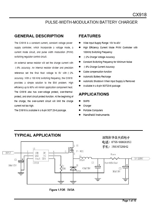
一、总体介绍1.简单说明是一颗车载充电器芯片,采用SOT23-6封装,输入范围10V ~40V (典型为12V 、24V ),输出为5V ,最大输出电流为3A/2A (具体值由检流电阻Rsen 决定)。
在负载很重时(Iload 需求>2A/1A ),实现恒流功能(CC ),Iload 实际=2A/1A ,设计精度8%;在负载较轻时(Iload<2A/1A ),实现恒压功能(CV ),V o=5V ,设计精度3%。
并带有OTP 、OVP 、OCP 、短路保护、cable 补偿,提供轻载工作模式。
2.应用电路CX918深圳市诚芯微科技有限公司 CX918二、测试数据1. 12V/24V 转5V (恒流1A )工作的I/V 曲线负载在1A 以内时,芯片工作在恒压模式下,输出稳定在4.85~5.15V,负载超过1A,输出降低,负载电流恒定供给1A,直到输出拉低到1.5V 左右,芯片关断(短路保护)不工作。
2. 线性调整率和负载调整率:线性调整率4.914.934.954.974.995.015.03101214161820222426283032343638输入电压(V)输出电压(V )Iout=0lout=1ACX918CX918负载调整率4.934.944.954.964.974.984.9955.0100.20.40.60.811.2负载电流(A)输出电压(V )VIN=12V VIN=24V3. 12V 转5V (恒流1A )测试数据及效率图 Vin(V)Iin(A) V out(V) Iout(A)效率 11.89 0.25 2 1.025 68.97% 11.88 0.2942.5 1.027 73.51% 11.84 0.345 3 1.028 75.50% 11.9 0.38 3.5 1.031 79.80% 11.87 0.425 4 1.033 81.91% 11.890.47 4.51.037 83.50%恒流工作效率60.00%65.00%70.00%75.00%80.00%85.00%1.522.533.544.55输出电压(V)效率CX918Vin(V) Iin(A) V out(V) Iout(A)效率 12.02 0.047 5 0.1 88.50% 11.98 0.116 4.98 0.25 89.59% 11.87 0.188 4.98 0.4 89.26% 11.82 0.237 4.97 0.5 88.71% 11.89 0.284 4.96 0.6 88.13% 11.83 0.36 4.96 0.75 87.35% 11.87 0.383 4.95 0.8 87.11% 11.91 0.485 4.941 85.52%恒压工作效率70.00%75.00%80.00%85.00%90.00%95.00%00.20.40.60.81负载电流(A)效率VIN=12V4. 24V 转5V (恒流1A )测试数据及效率图 Vin(V)Iin(A) V out(V) Iout(A) 效率 24.01 0.136 2 1.03 63.09% 24.01 0.158 2.5 1.033 68.08% 24.02 0.18 3 1.035 71.82% 24.02 0.202 3.5 1.037 74.80% 24.01 0.224 4 1.04 77.35% 24.010.2474.51.04579.29%CX918恒流工作效率60.00%65.00%70.00%75.00%80.00%85.00%1.52 2.53 3.54 4.55输出电压(V)效率Vin(V) Iin(A) V out(V) Iout(A)效率 24.03 0.025 5 0.1 83.23% 23.97 0.061 4.99 0.25 85.32% 23.95 0.098 4.98 0.4 84.87% 23.96 0.123 4.98 0.5 84.49% 23.91 0.149 4.97 0.6 83.70% 23.9 0.188 4.96 0.75 82.79% 23.94 0.201 4.96 0.8 82.46% 23.9 0.254 4.95 1 81.54%恒压工作效率70.00%75.00%80.00%85.00%90.00%95.00%00.20.40.60.81负载电流(A)效率VIN=24V三、 PCB 板布局建议:1. 流大电流的线要粗,短,不拐弯。
Agilent Technologies 85027A B C 方向桥操作和维修手册说明书
Agilent Technologies85027A/B/CDirectional BridgeOperation andService ManualAgilentTechnologiesREPRODUCTION AND DISTRIBUTION OFTHIS TECHNICAL MANUAL IS AUTHORIZEDFOR GOVERNMENT PURPOSES._________________________________________________________________________________ Operation and Service ManualThis Operation and Service Manual provides instructions on installing, operating, and servicing the Agilent Technologies Model 85027A/B/C Directional Bridges used with the Agilent Technologies Model 8757D-E02 Scalar Network Analyzer being delivered under U.S. Navy Contract NumberN00104-07-D-D014.Manual Part Number 85027-90048November 2007REPRODUCTION AND DISTRIBUTION OF THISTECHNICAL MANUAL IS AUTHORIZED FORGOVERNMENT PURPOSES.© Copyright Agilent Technologies 2007All Rights ReservedAGILENT TECHNOLOGIES INCDIVISION TMO CUSTOMER BUSINESS CENTER9780 S MERIDIAN BLVDENGLEWOOD CO 80112 – 5910Agilent Technologies 85027A/B/CDirectional BridgeHewlett-Packard to Agilent Technologies Transition This manual may contain references to HP or Hewlett-Packard. Please note thatHewlett-Packard's former test and measurement, semiconductor products and chemical analysis businesses are now part of Agilent Technologies. To reduce potential confusion, the only change to product numbers and names has been in the company name prefix: where a product number/name was HP XXXX the current name/number is now Agilent XXXX. For example, model number HP8648 is now model number Agilent 8648.Documentation WarrantyTHE MATERIAL CONTAINED IN THIS DOCUMENT IS PROVIDED "AS IS," AND IS SUBJECT TO BEING CHANGED, WITHOUT NOTICE, IN FUTURE EDITIONS. FUR-THER, TO THE MAXIMUM EXTENT PERMITTED BY APPLICABLE LAW, AGILENT DISCLAIMS ALL WARRANTIES, EITHER EXPRESS OR IMPLIED WITH REGARD TO THIS MANUAL AND ANY INFORMATION CONTAINED HEREIN, INCLUDING BUT NOT LIMITED TO THE IMPLIED WARRANTIES OF MERCHANTABILITY AND FIT-NESS FOR A PARTICULAR PURPOSE. AGILENT SHALL NOT BE LIABLE FOR ERRORS OR FOR INCIDENTAL OR CONSEQUENTIAL DAMAGES IN CONNECTION WITH THE FURNISHING, USE, OR PERFORMANCE OF THIS DOCUMENT OR ANY INFORMATION CONTAINED HEREIN. SHOULD AGILENT AND THE USER HAVE A SEPARATE WRITTEN AGREEMENT WITH WARRANTY TERMS COVERING THE MATERIAL IN THIS DOCUMENT THAT CONFLICT WITH THESE TERMS, THE WAR-RANTY TERMS IN THE SEPARATE AGREEMENT WILL CONTROL.DFARS/Restricted Rights NoticeIf software is for use in the performance of a U.S. Government prime contract or subcontract, Software is delivered and licensed as “Commercial computer software” as defined in DFAR 252.227-7014 (June 1995), or as a “commercial item” as defined in FAR 2.101(a) or as “Restricted computer software” as defined in FAR 52.227-19 (June 1987) or any equivalent agency regulation or contract clause. Use, duplication or disclosure of Software is subject to Agilent Technologies’ standard commercial license terms, andnon-DOD Departments and Agencies of the U.S. Government will receive no greater than Restricted Rights as defined in FAR 52.227-19(c)(1-2) (June 1987). U.S. Government users will receive no greater than Limited Rights as defined in FAR 52.227-14 (June 1987) or DFAR 252.227-7015 (b)(2) (November 1995), as applicable in any technical data.Printing Copies of Documentation from the WebTo print copies of documentation from the Web, download the PDF file from the Agilent web site:•Go to .•Enter the document’s part number (located on the title page) in the Quick Search box.•Click GO.•Click on the hyperlink for the document.•Click the printer icon located in the tool bar.Contacting AgilentThis information supersedes all prior HP contact information. Online assistance:/find/assistAmericasBrazil(tel) (+55) 11 3351 7012 (fax) (+55) 11 3351 7024Canada(tel) 888 447 7378(fax) 905 282 6495Mexico(tel)180****2440(fax)180****4222United States(tel)800 829 4444(alt)(+1) 303 662 3998(fax)800 829 4433 Asia Pacific and JapanAustralia(tel) 1 800 225 574 (fax) 1 800 681 776 (fax) 1 800 225 539China(tel) 800 810 0508(alt) 800 810 0510(fax) 800 810 0507(fax) 800 810 0362Hong Kong(tel) 800 933 229(fax) 800 900 701India(tel) 1600 112 626(fax) 1600 112 727(fax) 1600 113 040Japan (Bench) (tel) 0120 32 0119 (alt) (+81) 426 56 7799 (fax) 0120 01 2144Japan (On-Site)(tel) 0120 802 363(alt) (+81) 426 56 7498(fax) (+81) 426 60 8953Singapore(tel)180****0880(fax) (+65) 6755 1235(fax) (+65) 6755 1214South Korea(tel) 080 778 0011(fax) 080 778 0013Taiwan(tel) 0800 047 669 (fax) 0800 047 667 (fax) 886 3492 0779Thailand(tel) 1 800 2758 5822(alt) (+66) 2267 5913(fax) 1 800 656 336Malaysia(tel) 1800 880 399(fax) 1800 801 054EuropeAustria(tel) 0820 87 44 11* (fax) 0820 87 44 22Belgium(tel) (+32) (0)2 404 9340(alt) (+32) (0)2 404 9000(fax) (+32) (0)2 404 9395Denmark(tel) (+45) 7013 1515(alt) (+45) 7013 7313(fax) (+45) 7013 1555Finland(tel) (+358) 10 855 2100(fax) (+358) (0) 10 855 2923France(tel) 0825 010 700* (alt) (+33) (0)1 6453 5623 (fax) 0825 010 701*Germany(tel) 01805 24 6333*(alt) 01805 24 6330*(fax) 01805 24 6336*Ireland(tel) (+353) (0)1 890 924 204(alt) (+353) (0)1 890 924 206(fax)(+353) (0)1 890 924 024Israel(tel) (+972) 3 9288 500(fax) (+972) 3 9288 501Italy(tel) (+39) (0)2 9260 8484 (fax) (+39) (0)2 9544 1175Luxemburg(tel) (+32) (0)2 404 9340(alt) (+32) (0)2 404 9000(fax) (+32) (0)2 404 9395Netherlands(tel) (+31) (0)20 547 2111(alt) (+31) (0)20 547 2000(fax) (+31) (0)20 547 2190Russia(tel) (+7) 095 797 3963(alt) (+7) 095 797 3900(fax) (+7) 095 797 3901Spain(tel) (+34) 91 631 3300 (alt) (+34) 91 631 3000 (fax) (+34) 91 631 3301Sweden(tel) 0200 88 22 55*(alt) (+46) (0)8 5064 8686(fax) 020 120 2266*Switzerland (French)(tel) 0800 80 5353 opt. 2*(alt) (+33) (0)1 6453 5623(fax) (+41) (0)22 567 5313Switzerland (German)(tel) 0800 80 5353 opt. 1*(alt) (+49) (0)7031 464 6333(fax) (+41) (0)1 272 7373Switzerland (Italian) (tel) 0800 80 5353 opt. 3* (alt) (+39) (0)2 9260 8484 (fax) (+41) (0)22 567 5314United Kingdom(tel) (+44) (0)7004 666666 (alt) (+44) (0)7004 123123 (fax) (+44) (0)7004 444555(tel) = primary telephone number; (alt) = alternate telephone number; (fax) = FAX number; * = in country number 8/03/04。
丹东华奥电子有限公司LDA82C251汽车半导体说明书
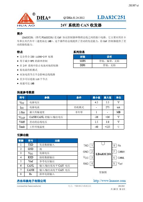
丹东华奥电子有限公司简介LDA82C251(替代PCA82C251)是CAN 协议控制器和物理总线之间的接口电路。
它主要应用在卡车和公共汽车中(速度高达1MB)。
这个器件给总线提供了差动的发送能力,给CAN 控制器提供了差动的接收能力。
特点系列信息●完全符合ISO 11898-24V 标准●用于减少RFI 的斜率控制●在24V 系统中防止电池对地的短路●低电流待机模式●未加电的节点不会影响总线线路●至少可以连接110个节点●高速可达1MB快速参考数据引脚功能封装说明SOP8管装,编带,无铅DIP8管装,无铅符号参数条件最小值最大值单位V CC 电源电压 4.5 5.5V I CC 电源电流待机模式-275uA 1/t bit 最大传输速度非归零1-MB V CAN CANH CANL 的输入/输出电压-36+36V Vdiff 差动的总线电压 1.5 3.0V Tamb工作环境温度-40+125℃管脚符号功能1TXD 发送数据输入2GND 地3V CC 电源电压4RXD 接收数据输出5Vref 参考电压输出6CANL 输入/输出低电平CAN 电压7CANH 输入/输出高电平CAN 电压8Rs斜率电阻输入LDA82C251管脚图24V 系统的CAN 收发器丹东华奥电子有限公司方框图电特性-40≤Tamb ≤+125符号参数条件最小值最大值单位电源I 3电源电流显性;V 1=1V;V CC <5.1V -78mA显性;V 1=1V;V CC <5.25V -80显性;V 1=1V;V CC <5.5V-85隐性;V 1=4V;R 8=47kΩ-10待机;注1-0.315待机;注20.275DC 总线发送器V IH 高电平输入电压输出隐性0.7V CC V CC +0.3V V IL 低电平输入电压输出显性-0.30.3V CC V I IH高电平输入电流4.5V<V CC <5.5V,V1=4.0V-20030μA丹东华奥电子有限公司丹东华奥电子有限公司电参数的典型值功能描述LDA82C251集成电路是提供差动发送能力的总线和差动接收能力的CAN控制器。
5V3A车充方案,5V2A车充方案
NS6112 效率测试 VIN VOUT 电压(V) 电流(A) 电压(V) 电流(A)
12.00 24.00 12.00 24.00 0.96 0.48 1.19 0.59 5.41 5.31 5.53 5.44 2.00 2.00 2.40 2.40
备注 效率(%)
93.92 92.18 92.94 92.20
总3页 第二页
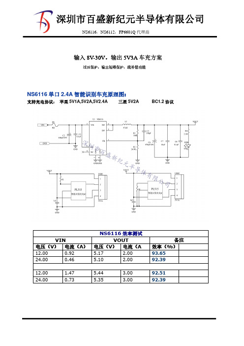
深圳市百盛新纪元半导体有限公司
NS6116,NS6112,FP6601Q 代理商
市百盛新纪元半导体有限公司
NS6116,NS6112,FP6601Q 代理商
输入 8V-30V,输出 5V3A 车充方案
过压保护,输出短路保护,线补偿功能
NS6116 单口 2.4A 智能识别车充原理图:
支持充电协议: 苹果 5V1A,5V2A,5V2.4A 三星 5V2A BC1.2 协议
VIN 电压(V) 电流(A)
深圳市百盛新纪元半导体有限公司
NS6116,NS6112,FP6601Q 代理商
输入 8V-30V,输出 5V2.4A 车充方案
过压保护,输出短路保护,线补偿功能
NS6112 单口 2.4A 智能识别车充原理图:
支持充电协议: 苹果 5V1A,5V2A,5V2.4A 三星 5V2A BC1.2 协议
12.00 24.00 12.00 24.00 0.92 0.46 1.47 0.73
NS6116 效率测试 VOUT 电压(V) 电流(A
5.17 5.10 5.44 5.35 2.00 2.00 3.00 3.00
备注 效率(%)
93.65 92.39 92.51 92.39
总3页 第一页
CT3582芯片资料
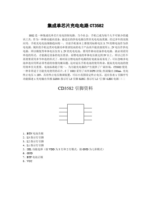
集成单芯片充电电路CT3582
3582是一种集成化单芯片充电控制电路。
当今社会,手机已成为每个人不可缺少的通讯工具。
作为一种移动通讯设备,最适宜的供电电源自然非充电电池莫属。
经过多年的实践应用,手机充电电池规格趋向统一,目前手机基本上都使用标称电压3.7V的锉电池作为供电电源。
现阶段手机这类对电源功率要求较高的电子产品尚不能直接使用1 .2V电压作供电电源,所以镍氢等单体电压仅有1.2V的充电电池,要用作移动设备供电电源,就必须采用串连的形式,才能满足设备的电压需求。
而铿电池的单体电压就达到3V以上,所以已经不再需要采用多节串连的形式了。
相对而言锉电池作电源的好处就显而易见了,可以忽略多电池串连应用所必须考虑的容量均衡问题。
这对延长手机电池的使用寿命,提高充电电池的使用效率至关重要。
电池标准趋于统一,为万能充电器的产生提供了广阔市场。
CT3582便是一种非常适于万能充电使用的芯片。
C丁3582采用了双列DIPS封装;恒流输出200mA,充电终止电压4.25V,具有终止电压微调装置,可以小范围设定终止电压,适应各表1引脚序号功能描述1充电输出负极2LEO3:指示灯L3引脚3LEOZ:指示灯L2弓}脚4LEDI电源(本文
CD3582引脚资料
1、BTN电池负极
2、L3指示灯引脚
3、L2指示灯引脚
4、L1指示灯引脚
5、SEL功能选择(接VDD为3灯和2灯模式,接GND为七彩模式)
6、GND
7、BTP电池正极
8、VCC。
CX3300 系列电流电压波形分析仪产品简介

1 A
PMIC
A 2 3 A浪涌ຫໍສະໝຸດ 未知瞬态过多电流消耗
电流
极大的浪涌
未知尖峰
意外状态
SoC/MCU
存储器
未知尖峰 未知瞬态
电池
4
A
A 5
休眠 唤醒 深度休眠
平均电流
显示器/ 传感器/ 致动器
接口
时间
处理
图 3. 典型方框图。
图 4. PDN 电流曲线概念图。
降低低功率物联网设备的功耗
低功率物联网和移动设备为了节省总功耗,通常只会短时间激活,而大部分时间均处于休眠/ 待机状态(见图 5)。平均电流测量是所有这些低功率设备的一项基本特征,但如果您想要进 一步降低功耗,这还不够。由于休眠/待机状态将持续更长时间以减少功率,因此不仅需要在 激活状态下进行更详细和定量的动态电流测量,在休眠/待机期间也需要进行同样的测量。休 眠/待机状态下的电流消耗通常只有 1 μA 甚至更低。
联系我们:
页 05
电流曲线 i
活动 (平均电流) t 休眠/待机
i
当需要降低更多 电流消耗时
i
放大 i
放大 i
降低休眠/待机电流(<1 μA 水平)
减少活动电流/持续时间(>1 mA 水平)
图 5. 低功率物联网设备的典型工作特征和进一步功率降低。
新型 NVM 器件的表征
车载 ECU
汽车传感器
RRAM/PCM/MRAM
图 2. CX3300 系列的应用实例。
半导体
图像传感器
笔记本电脑
能源采集
联系我们:
页 04
对精确动态电流测量的迫切需求
物联网和移动设备中的 PDN(电源分配网络)的表征和验证
车充IC-CX8518 32V 3.5A DC-DC芯片
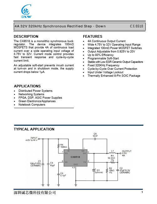
VIN Rising
Input Under Voltage Lockout Threshold Hysteresis
Soft-Start Current
Soft-Start Period Thermal Shutdown (5)
VSS = 0V CSS = 0.1µF
Min
Typ
Max Units
2.2
VIN = 12V, TA = +25°C, unless otherwise noted.
Parameter
Symbol Condition
EN Lockout Threshold Voltage
EN Lockout Hysterisis
Input Under Voltage Lockout Threshold
3
SW the output LC filter from SW to the output load. Note that a capacitor is required from SW to
BS to power the high-side switch.
4.5
GND Ground
Feedback Input. FB senses the output voltage and regulates it. Drive FB with a resistive
Recommended Operating Conditions (2)
Input Voltage VIN............................ 4.75V to 32V Output Voltage VOUT .................... 0.925V to 20V Ambient Operating Temp .............. –40°C to +85°C
LT8309 二次侧同步充电驱动器说明书

Typical applicaTionFeaTuresDescripTionSynchronous Rectifier DriverThe L T ®8309 is a secondary-side synchronous rectifier driver that replaces the output rectifier diode in a flyback topology. By replacing the diode with a N-channel MOSFET, applications are no longer restricted by the heat constraints of the output diode. The IC replicates the behavior of a diode by sensing the drain-to-source voltage to determine when the current becomes negative. The LT8309's low minimum on- and off-times help improve noise immunity. The fast propagation delay of 26ns allows applications to operate in discontinuous conduction mode (DCM) and critical conduction mode (CrCM). The gate driver features a 0.8Ω pull-down device for fast turn-offs. The 40V V CC rating allows the part to be driven from the output volt-age or the rectified drain voltage of the MOSFET. A low quiescent current of 400µA maximizes efficiency at low output currents.40W, 5V Isolated Telecom SupplyEfficiency vs Load CurrentapplicaTionsnWorks with DCM and BCM/CrCM Conduction Mode Flyback Topologies n V CC: 4.5V to 40V n Supports Up to 150V MOSFETs n 26ns Turn-Off Propagation Delayn Accurate Minimum On and Off Timers for Reliable Operationn Adjustable and Accurate T rip Point: +5mV to –30mV n 1Ω Gate Driver Pull-Down n SOT-23 5-Lead PackagenHigh Output Current Flybacks n High Efficiency FlybacksL , L T, L TC, L TM, Linear Technology and the Linear logo are registered trademarks ofLinear Technology Corporation. All other trademarks are the property of their respective owners.OUT +, 8AOUT –VLOAD CURRENT (A)065E F F I C I E N C Y (%)708090123465775851009588309 TA01bpin conFiguraTionabsoluTe MaxiMuM raTingsV CC ............................................................................40V INTV CC GATE ............................................................10V DRAIN .....................................................................150V Maximum Junction Temperature ..........................125°C Operating Temperature Range (Note 2)LT8309E ............................................–40°C to 125°C LT8309I .............................................–40°C to 125°C LT8309H ............................................–40°C to 150°C Storage Temperature Range ..................–65°C to 150°C(Note 1)GATE 1GND 2TOP VIEWS5 PACKAGE5-LEAD PLASTIC TSOT-23INTV CC 35 DRAIN4 V CCθJA = 215°C/WorDer inForMaTionLEAD FREE FINISH TAPE AND REEL PART MARKING*PACKAGE DESCRIPTION TEMPERATURE RANGE LT8309ES5#PBF LT8309ES5#TRPBF L TGFZ 5-Lead Plastic TSOT-23–40°C to 125°C LT8309IS5#PBF LT8309IS5#TRPBF L TGFZ 5-Lead Plastic TSOT-23–40°C to 125°C LT8309HS5#PBFLT8309HS5#TRPBFL TGFZ5-Lead Plastic TSOT-23–40°C to 150°CConsult L TC Marketing for parts specified with wider operating temperature ranges. *The temperature grade is identified by a label on the shipping container.For more information on lead free part marking, go to: /leadfree/For more information on tape and reel specifications, go to: /tapeandreel/elecTrical characTerisTicsNote 1: Stresses beyond those listed under Absolute Maximum Ratings may cause permanent damage to the device. Exposure to any Absolute Maximum Rating condition for extended periods may affect device reliability and lifetime.Note 2: The LT8309E is guaranteed to meet performance specifications from 0°C to 125°C operating junction temperature. Specifications over the –40°C to 125°C operating junction temperature range are assured by design, characterization and correlation with statistical process controls. The LT8309I is guaranteed over the full –40°C to 125°C operating junctionPARAMETER CONDITIONSMIN TYP MAX UNITSInput Voltage Range l4.540V V CC Quiescent Current Not Switching, INTV CC = 8V 300345µA Comparator Turn-On Threshold R S = 0Ωl –69–57–45mV Turn-Off Threshold R S = 0Ω l17 162125 28mV mV Drain Voltage Latch Reset R S = 0Ω1.21V Minimum Off-Time 7595115ns Minimum On-Time 310360410ns Drain CurrentOut of Pinl 9.51010.5µA INTV CC Linear Regulator INTV CC Quiescent Current Not Switching, INTV CC = 8V100117µA INTV CC Voltage Range 4.510V INTV CC Regulation Voltage l6.877.2V INTV CC UVLO4.03V Dropout (V CC to INTV CC )I INTVCC = –10mA, V IN = 7V1 1.3 1.6V Current Limit l 304255mAGate DriverTurn-On Propagation Delay (t D(ON))R S = 0Ω, –100mV OD , V DS to V GATE 3140ns Turn-Off Propagation Delay (t D(OFF))R S = 0Ω, –100mV OD , V DS to V GATE 2636ns t r GATE Driver Output Rise Time C L = 3300pF 21ns t f GATE Driver Output Fall Time C L = 3300pF11ns Pull-Up Resistance 2.7ΩPull-Down Resistance0.8ΩThe l denotes the specifications which apply over the full operating temperature range, otherwise specifications are at T A = 25°C.temperature range. The LT8309H is guaranteed over the full –40°C to 150°C operating junction temperature range. High junction temperatures degrade operating lifetimes. Operating lifetime is derated at junction temperatures greater than 125°C.Note 3: The LT8309 includes overtemperature protection that is intended to protect the device during momentary overload conditions. Junction temperature will exceed 150°C when overtemperature protection is active. Continuous operation above the specified maximum operating junction temperature may impair device reliability.TEMPERATURE (°C)–500V C C I Q C U R R E N T (µA )50150250–252550100751251002003504503004001508309 G01TEMPERATURE (°C)–50I N T V C C I Q C U R R E N T (µA )–252550100751251508309 G02408012016020020601001401800I N T V C C V O L T A G E (V )24681357V CC VOL TAGE (V)102030408309 G04TEMPERATURE (°C)–503.0T H R E S H O L D V O L T A G E (V )3.54.5–252550100751255.04.01508309 G05INTV CC CURRENT (mA)I N T V C C R E G U L A T O R D R O P O U T (V )1.51020302.51.00.52.0408309 G06TEMPERATURE (°C)–500I N T V C C D R O P O U T (V )1.0–252550100751252.00.51.51508309 G07TEMPERATURE (°C)–500I N T V C C C U R R E N T L I M I T (m A )103050–252550100751252040601508309 G08Typical perForMance characTerisTicsINTV CC Voltage vs V CC VoltageINTV CC Undervoltage Lockout vs TemperatureINTV CC Regulator Dropout vs INTV CC CurrentINTV CC Dropout vs TemperatureINTV CC Current Limit vs TemperatureMinimum On-Time and Off-Time vs TemperatureI VCC vs TemperatureI INTVCC vs TemperatureINTV CC vs TemperatureTEMPERATURE (°C)–100–50T I M E (n s )501001502008309 G0950150250100200350300400TEMPERATURE (°C)–506.0I N T V C C V O L T A G E (V )6.46.87.2–252550100751258.07.86.26.67.07.47.61508309 G03TEMPERATURE (°C)–500D R A I N P I N C U R RE N T (µA )2612–252550100751251048141508309 G10TEMPERATURE (°C)–50T U R N -O N T H R E S H O L D (m V )–252550100751251508309 G11–80–70–60–50–40–75–65–55–45TEMPERATURE (°C)–50T U R N -O F F T H R E S H O L D (m V )–252550100751251508309 G12102030405152535TEMPERATURE (°C)–501.00T H R E S H O L D V O L T A G E (V )1.101.201.30–252550100751251.401.051.151.251.351508309 G13Typical perForMance characTerisTicsLatch Reset Thresholdvs TemperatureGATE Rise and Fall Time vs ChargeGATE Current vs ChargeDRAIN Pin Current vs TemperatureComparator Turn-On Thresholdvs TemperatureComparator Turn-Off Threshold vs Temperature0T I M E (n s )50150200100CHARGE (nC)6012030901508309 G14T I M E (n s )1.02.03.04.00.51.52.53.5CHARGE (nC)8309 G150601203090150block DiagraMpin FuncTionsGATE (Pin 1): N-Channel MOSFET Gate Driver Output. Switches between INTV CC and GND. Driven to GND during undervoltage lockout of INTV CC . GND (Pin 2): Ground.INTV CC (Pin 3): Regulated Supply for Internal Loads, and GATE Driver. Supplied from V CC and regulates to 7V (typical). INTV CC must be bypassed with a 4.7µF capacitor placed close to the pin.V CC (Pin 4): Input Voltage. This pin supplies current to the internal start-up circuitry and to the INTV CC LDO. This pin must be locally bypassed with a capacitor.DRAIN (Pin 5): Current Sense Pin. This pin sensesthe voltage across the drain-to-source of the externalN-channel MOSFET. A series resistor is needed to set the offset voltage and needs to be at least 800Ω. The offset is equal to:20mV •1−R 20008309 F01GND V OFFSETD(ON)D(OFF)operaTionThe LT8309 is a synchronous rectifier designed for boundary conduction mode/critical conduction mode and discontinuous mode flyback converters. Existing solutions use a pulse signal from the primary side to control the synchronous rectifier, but the LT8309 senses the drain-source voltage of the MOSFET to control the synchronous rectifier. This technique not only elimi-nates a transformer, but allows it to work with Linear Technology’s line of no-opto critical conduction flyback converters. Synchronous rectification improves ef-ficiency and more importantly increases the maximum output current when compared to nonsynchronous designs.The LT8309 imitates the behavior of a diode but re-places the forward voltage with the R DS(ON) of an externalN-channel MOSFET. The LT8309 includes an LDO, a very fast comparator and a powerful gate driver.An external resistor connects the part’s DRAIN pin to the drain of the MOSFET. This resistor sets the trip point of the comparator with a precise internal current source. To set the trip point to –10mV, a 3000Ω resistor is needed. The trip point decreases by 1mV for every 100Ω added to this drain resistor. This trip point will be referred to as V OFFSET . Figure 1 shows the drain waveform on top and the gate waveform on the bottom. The gate node goes high when the drain node goes 74mV below the V OFFSET . The comparator’s output is ignored for a minimum on-time to eliminate the chance that ringing triggers the comparator. After the minimum on-time, the comparator is ready to trigger at the V OFFSET voltage. Once the drain voltage goes above V OFFSET , the gate turns off after a very fast propaga-tion delay, t D(OFF). The body diode begins to conduct again before the current reaches 0A. The drain voltage needs to go above 1.21V and then wait for the minimum off-time before the comparator is re-enabled.Figure 1. Drain and Gate WaveformsOUTV operaTionUndervoltage LockoutThe part features a INTV CC undervoltage lockout (UVLO) to prevent switching until the INTV CC voltage is above 4V. INTV CC LDOAn internal LDO regulator provides a regulated 7V output from the V IN pin to the INTV CC pin. An output capacitor is needed to provide the current needed for the gate driver. A 4.7µF capacitor is recommended and must be placed as close as possible to the INTV CC pin. The current limit for the LDO is 42mA.MOSFET SelectionA MOSFET’s R DS(ON) is important to the operation of the LT8309. The drain-source voltage is used to determine when to turn off the MOSFET. The peak current through the MOSFET times the MOSFET’s R DS(ON) should be above 75mV. When this voltage is too low, the high speed comparator may trip early due to ringing on the DRAIN pin. When this voltage is too high, the MOSFET dissipates a large amount of power which causes efficiency to go down and may cause thermal issues with the MOSFET.Setting the DRAIN Pin ResistorThe DRAIN pin resistor sets when the LT8309 turns off the MOSFET. The trip point, V OFFSET , is set with the fol-lowing equation:V OFFSET = 20mV – 10µA • R DRAINR DRAIN is the resistor connected between the drain of the MOSFET and the DRAIN pin of the part. R DRAIN needs to be at least 800Ω to operate correctly. For most applications, V OFFSET should be set at –5mV. High R DS(ON) MOSFETs may require a more negative V OFFSET voltage to keep the drain-to-source current from reversing. If the current is reversing, decrease V OFFSET in 5mV steps to eliminate the cross-conduction. Short-Circuit OperationIn the Typical Application diagram on Page 1, the V CC pin is connected to the output of the flyback converter. During an output short-circuit condition, the LT8309 is off and the body diode of the MOSFET must handle the short-circuit condition. This puts additional thermal requirements on the MOSFET. The drain voltage of the MOSFET is equal to V IN /N in short-circuit and capable of powering the LT8309 with the circuit in Figure 2. This allows the LT8309Figure 2. Short-Circuit Application CircuitoperaTionFigure 3. Demo Board Topside Silkscreen Figure 4. Demo Board Topside Metalto operate during a short, and the current will flow throughthe low resistance channel of the MOSFET instead of itsbody diode. Make sure to use a resistor in series with thediode to keep V CC below 40V.Layout ConsiderationsThe main current loop is the MOSFETs drain-to-sourcecurrent. This should not share the same ground path asthe LT8309. The drain resistor needs to sense directly atthe drain of the MOSFET and not have any current of thedrain current flow through its metal trace. The drain nodeof the MOSFET is used as the heat sink and will need tobe sized according to the power dissipation requirements.Figure 3 is an example layout of the LT8309.Effects of the Body DiodeWhen the discontinuous ring voltage goes below ground,the body diode of the primary-side MOSFET turns on andbegins to conduct current. This diode clamps the voltageto a diode drop below ground. When the current reversesdirection, the diode does not turn off immediately, andconducts current in the opposite direction for a small periodof time. This is known as the reverse-recovery time. Duringthis time, the magnetizing inductance of the transformerstores energy just like it does when the MOSFET turnson. When the primary-side body diode finally turns off,the energy is transferred to the secondary side and maybe enough to turn on the body diode of the secondaryMOSFET. Then, the LT8309 turns on its MOSFET for asecond time. Since this happens during the discontinuousring, the primary side may turn on during this time andcause cross conduction. If this problem does occur, oneway to improve the reverse-recovery time of the primaryside’s MOSFET is to add a parallel Schottky diode, whichwill conduct most of the current and turn off much fasterthan the body diode. Another way of eliminating this issueis by sizing the turns ratio so that the discontinuous ringnever goes below ground.Typical applicaTions60W, 12V Output, Isolated Telecom SupplyV, 5AOUT–Typical applicaTions40W, 5V Isolated Telecom SupplyV, 8AOUT–118309faFor more information /L T8309package DescripTionPlease refer to /designtools/packaging/ for the most recent package drawings.0.30 – 0.45 TYP5 PLCS (NOTE 3)(NOTE 3)S5 TSOT-23 0302 NOTE:1. DIMENSIONS ARE IN MILLIMETERS2. DRAWING NOT TO SCALE3. DIMENSIONS ARE INCLUSIVE OF PLATING4. DIMENSIONS ARE EXCLUSIVE OF MOLD FLASH AND METAL BURR5. MOLD FLASH SHALL NOT EXCEED 0.254mm6. JEDEC PACKAGE REFERENCE IS MO-1930.620.95RECOMMENDED SOLDER PAD LAYOUTPER IPC CALCULATORS5 Package3-Lead Plastic TSOT-23(Reference LTC DWG # 05-08-1635)128309faFor more information /L T8309138309faFor more information www.linear .com/L T8309Information furnished by Linear Technology Corporation is believed to be accurate and reliable. However, no responsibility is assumed for its use. Linear Technology Corporation makes no representa-tion that the interconnection of its circuits as described herein will not infringe on existing patent rights.revision hisToryREV DATE DESCRIPTION PAGE NUMBERA11/14Added H-Grade Version2, 3148309faFor more information www.linear .com/L T8309LINEAR TECHNOLOGY CORPORA TION 2014LT 1114 REV A • PRINTED IN USALinear Technology Corporation1630 McCarthy Blvd., Milpitas, CA 95035-7417(408) 432-1900 ● FAX : (408) 434-0507 ● www.linear .com/L T8309relaTeD parTsTypical applicaTionPART NUMBER DESCRIPTIONCOMMENTSLT3748100V Isolated Flyback Controller5V ≤ V IN ≤ 100V, No-Opto Flyback, MSOP-16 PackageLT3798Offline Isolated No-Opto-Coupler Flyback Controller with Active PFCV IN and V OUT Limited Only by External Components, MSOP-16 Package LT3799/LT3799-1Offline Isolated Flyback LED Controller with Active PFC V IN and V OUT Limited Only by External Components, MSOP-16 Package LT3957A/LT395840V/80V Flyback/Boost/Inverting/SEPIC Converter Monolithic with Integrated 5A/3.3A SwitchLT3573/LT3574/ LT357540V Isolated Flyback ConvertersMonolithic No-Opto Flybacks with Integrated 1.25A/0.65A/2.5A Switch LT3757A/LT3759/ LT375840V/100V Boost, Flyback, SEPIC and Inverting Controllers Universal Controllers with Small Package and Powerful Gate Drive LT8302Micropower No-Opto Isolated Flyback Converter2.8V ≤ V IN ≤ 42V, with Integrated3.6A, 65V DMOS Power Switch, 106µA Quiescent Current, SO-8 Package33W, 3.3V Isolated Telecom SupplyOUT +, 10AOUT –V。
WT588F02B-8S 语音芯片说明书
广州唯创电子有限公司MP3录音模块WT588F02B-8S语音芯片说明书V1.07免责申明:深圳唯创知音电子有限公司申明;说明书以官网资料为准,如若资料内容有更新,不会一一进行通知。
如若使用IC时导致侵犯到第三方专利或其他权利,不承担任何责任。
如若使用我司IC,在航空卫星军事设备,人身安全等领域,造成了重大财产损失或生命伤害,甚至生命死亡,我司不承担任何责任。
目录说明书以官网和业务员提供为准 (1)版本记录: (1)1.概述: (2)2.功能简述: (2)3.管脚描述: (3)4.极限参数: (3)5.电气特性: (4)6.一线串口通讯: (4)7.两线串口通讯: (7)8.程序范例 (10)9.封装管脚图 (13)10.客户在线下载器 (14)说明书以官网和业务员提供为准版本记录:版本号修改说明修改日期V1.00原始版本2020-8-24V1.01指令部分说明完善2020-9-11V1.02修改部分说明完善2020-9-17V1.03修改DAC部分原理图2020-10-21V1.04将原理图做成独立的文档2020-11-06V1.05修改芯片待机功耗部分说明2020-11-12V1.06封装图修改2021-04-26V1.07单双字节指令码说明2021-07-241.概述:WT588F02B-8S是深圳唯创知音电子有限公司最新研发的一款16位DSP语音芯片、内部振荡32Mhz,16位的PWM解码。
强大功能让WT588F02B-8S成为语音芯片行业中的佼佼者。
目前WT588F02B-8S,较高音质最大可以支持存放170秒语音内容(若客户对音质没有要求,最大可以存放320秒的语音内容)。
WT588F02B-8S区别于传统OTP芯片,最大的突破是客户可以自己通过配套下载器实现在线更换芯片内部语音内容;并且芯片内置硬件SPI、UART、IIC、比较器等各类资源,可以为客户定制各种不同的个性化功能产品。
CX918 车充芯片车充方案
PULSE-WIDTH-MODULATION BATTERY CHARGERGENERAL DESCRIPTIONThe CX918 is a constant current, constant voltage power supply controller, which incorporate a voltage mode, a current mode circuit, and pulse width modulation (PWM) switching regulator control circuit.An external sense resistor will set the charge current with ±8% accuracy. An internal resistor divider and precision reference set the final float voltage to 5V with ±2% accuracy. With a 100 KHz switching frequency, the CX918provides a simple solution to the EMI problem. High efficiency up to 90% will minish application component heat. The CX918 also has over-voltage protect, over-thermal protect, and short circuit protect function. At the beginning of the charge, the over-current circuit will limit the charge current not too high.The CX918 is available in a 6-pin SOT 23-6 package.FEATURESz Wide Input Supply Range: 10V to 40Vz High Efficiency Current Mode PWM Controller with100KHz Switching Frequency z ±2% Charge Voltage Accuracyz Constant Switching Frequency for Minimum Noise z ±8% Charge Current Accuracy z Cable compensation function z Automatic Battery Rechargez Automatic Shutdown When Input Supply is Removed z Available in a 6-pin SOT23-6 packageAPPLICATIONSz SMPS z Chargerz Portable Computers z Handheld InstrumentsTYPICAL APPLICATIONFigure 1.FOR 5V/3ACX918PIN CONFIGURATIONSTOP VIEWFigure2 Pin configurationPIN DEFINITIONPIN NAMEDESCRIPTION1 V IN Power Supply Input. 2GNDThe ground of IC.3 V OUTOutput power supply. Connect to the external charge equipment. Note14 SENOutput Voltage feedback . 5 V CABLEConnect an equal resistor to set the compensation voltage and improve the output power which the cable wasted.If float this pin, cable compensation function will not work.6 DRVGate Drive Output. Driver output for the external P-Channel MOSFET. The voltage atthis pin is internally clamped to 8V below V IN .Note1: V OUT can be programmed to compensate the wasting voltage of cable.ABSOLUTE MAXIMUM RATINGSPARAMETER SYMBOL MIN MAX UNITSInput Supply VoltageV IN 10 Operating Temperature Range T OPR -40 85 °C Storage Temperature Range T STG -20 125 °C Junction TemperatureθJA --- 125 °C Lead Temperature (Soldering, 10s)T LTG --- 260 °C40 VCX918ELECTRICAL CHARACTERISTICSTYPICAL OPERATING CHARACTERISTICS(Circuit of Figure 1,T A = 25°C, V IN=12V, V OUT=5V, unless otherwise noted.)Efficiency vs Load Current Efficiency vs Load CurrentOutput Voltage vs Input Voltage Output Voltage vs Input Voltage10121416182022242628304.904.914.924.934.944.954.964.974.984.995.00O u t p u t V o l t ag e [V ]Input Voltage[V]1012141618202224262830O u t p u t V o l t a g e [V ]Input Voltage[V]Output Ripple Voltage vs Input Voltage Output Ripple Voltage vs Input Voltage 101214161820222426283040455055606570O u t p u t R i p p l e V o l t a g e [m V ]Input Voltage[V]101214161820222426283040455055606570O u t p u t R i p p l e V o l t a g e [m V ]Input Voltage[V]Output Ripple Voltage vs Input Voltage Output Ripple Voltage vs Input Voltage101214161820222426283040455055606570O u t p u t R i p p l e V o l t a g e [m V ]Input Voltage[V]1012141618202224262830O u t p u t R i p p l e V o l t a g e [m V ]Input Voltage[V]Cable compensation vs Load Current Quiescent current vs Input Voltage20040060080010000100200300400500600700C a b l e C o m p e n s a t i o n V o l t a g e [m V ]Load Current[mA]1012141618202224262830150152154156158160162164166168170Q u i e t C u r r e n t [u A ]Input Voltage[V]FUNCTION DIAGRAMOPERATIONIntroductionThe CX918 is designed to be a power supply control; it incorporates a constant current circuit and a constant voltage circuit.The charge current is set by an external sense resistor (RSEN) across the SEN and V OUT pins. The final output voltage is internally set to 5V, the internal amplifier and resistor divider provide regulation with ±2% accuracy.Start-UpWhen system detect the input power connect to IC, the internal start-up circuit will send a signal to and enable the IC. If the input voltage is below 4V, the IC should not start up.Constant Current and Voltage circuitDuring normal operation, the constant current charge loop start-up at first, but it will be replaced by the constant voltage loop, when the output voltage is higher than design (5V). In the constant current loop, the average current of inductor is set to be followed the external sense resistor. This constant current function controlled by error amplifier I-EA, and the amplifier make sure the current ±5% accuracy. In the voltage loop, system regulate SEN voltage by switching at a constant frequency transferring the power to the load in each cycle, uses a slope circuit, voltage mode PWM controller.A simplified function diagram of charge current and charge voltage is shown in Figure 4:Cable CompensationThe cable of car charger will lose some power, reducing the output voltage. Add voltage compensation function will increase the output voltage and make the output of cable is remained to be the design value. An external resistor will be connected to the VCABLE pin to matching the immanent resistor of cable. In the cable compensation circuit, the voltage of the VCABLE pin will be raised as the load current increase; the reference voltage of voltage loop will be raised to an appropriate value, and finished the compensation function.If there’s no load, no compensation resistor or output current is zero, the output voltage don’t rise. If not use this function, let the VCABLE pin hang in the air. The selection of external compensation resistor is based on the equivalent resistance of cable. The relation of compensation voltage and resistor is as the formula 1.SENLOAD CABLECABLE R I R KV ××=1500Formula1 Over Voltage protectionWhen the output voltage of CX918 is 10% higher then the design voltage, the PMOS will be turned off.Thermal ShutdownAn internal thermal loop can monitors the die temperature. If the die temperature attempts to rise above a preset value ofapproximately 120℃, it can turn off the charge. This feature protects the CX918 from excessive temperature and allows the user to push the limits of the power handling capability of a given circuit board without risk of damaging the CX918.Short Circuit protectionAt the beginning of enable the IC, system will charge the load about 100ms. If the short circuit protection module detect the output voltage is fall down 1.5V, it will send a single to logic circuit for shut down the IC. When short circuit happened, a current about 2 mA will charge the load. If the short circuit state is resumed, the charge current will raise output above 1.5V, and the module will detect it and free from protecting state.Over Current ProtectionCX918 has an internal over-current protection circuit that limits the inrush current during start-up. At the beginning of the start-up, the over-current protection circuit will detect the current, if it’s too high to exceed the safe value, the PMOS will be turn-off. But when output is rise to the design voltage, the protect function will not active anymore. The I-EA will replace the function to limiting the current.APPLICATION INFORMATIONThe basic application circuit of CX918 is shown in Figure 1. External components selection is depend on load requirement, and begin with the selection of inductor followed by capacitor.CX918Inductor SelectionThe inductor is chosen based on the desired ripple current. Large value inductors result in lower ripple current and small value inductors result in higher ripple current. Higher V IN or V OUT also increases the ripple current. Always consider the losses associated with the DCR and its effect on the total converter efficiency when selecting an inductor. For most designs, the CX918 operates with inductors of 100uH, the inductor is selected to limit the ripple current to some predetermined value, typically 20~40% of the full load current at the maximum input voltage. The formula of inductance value is as below:fL V V LIINOUT ×−×=Δ/1K (K= 0.2~0.4) Formula 2⎟⎟⎠⎞⎜⎜⎝⎛−Δ×=IN OUT LOUTV V If V L 1 Formula 3The DC current rating of the inductor should be at least equal to the maximum load current plus half the ripple current to prevent core saturation. For example, △I L =1000mA×40%=400mA, thus, a 1400mA rated inductor should be enough for most application (1000mA+400mA). For better efficiency, choose a low DCR inductor.Input Capacitor SelectionThe input capacitor reduces the surge current drawn from the input and switching noise from the device. The input capacitor impedance at the switching frequency shall be less than input source impedance to prevent high frequency switching current passing to the input. A low ESR input capacitor sized for maximum RMS current must be used. A 100uF ceramic capacitor for most application is sufficient.Output Capacitor SelectionThe output capacitor is required to keep the output voltage ripple small and to ensure regulation loop stability. The output capacitor must have low impedance at the switching frequency. Ceramic capacitors with X5R or X7R dielectrics are recommended due to their low ESR and high ripple current. The output ripple V OUT is determined by the formula below:⎟⎟⎠⎞⎜⎜⎝⎛+Δ=ΔOUT L OUT fC ESR I V 81 Formula 4 Load Current limit ProgrammingThe constant current I CHG is programmed with a sense resistor connected between the inductor and output. The voltage drop of the resistor (RSEN) is internally regulated to 50mV, which sets the current flowing through R SEN .For the best accuracy, a 2% or better resistor is recommended. Table 1 shows several typical 1% R SEN values.I CHG (mA)R SEN (m Ω) 2000 251000 50For other constant current values, use the following equation to choose R SEN :OUTSENI R05.0=Formula 5The application circuit of limiting 2A load current as follow.PACKAGE DESCRIPTIONDimensions In Millimetres Dimensions In InchesSymbol Min Max Min Max A 1.050 1.250 0.041 0.049 A10.000 0.100 0.000 0.004 A2 1.050 1.150 0.041 0.045 b 0.300 0.500 0.012 0.020 c 0.100 0.200 0.004 0.008 D 2.820 3.020 0.111 0.119 E 1.500 1.700 0.059 0.067 E1 2.650 2.950 0.104 0.116e 0.950(BSC) 0.037(BSC) e1 1.800 2.000 0.071 0.079 L 0.300 0.600 0.012 0.024 θ0° 8° 0° 8°ADJ TYPICAL APPLTCATIONCX918。
SM8502开关电源芯片说明书
地址:深圳市高新技术产业园南区高新南一道国微大厦5楼ADD: Shenzhen High-tech Industrial Park,South Area GaoxinS.Ave.1st,Guowei Building.电话Tel:0755-******** 传真Fax:0755-******** 邮编:518057网址:离线式开关电源开关芯片SM8502一、 概述:SM8502是一款工作于交流宽电压输入的离线式原边反馈AC/DC控制芯片。
应用系统只需很少外围器件就能实现非常精确的原边控制,并且达到全球节能标准,系统待机功耗小于300mW。
SM8502无需光耦和其它相关控制器件就能实现精确的恒压和恒流控制。
SM8502内置了多种保护电路,包括:输出短路保护、输入欠压保护、输出过压保护和过温保护等,保证系统安全工作。
二、 特色说明:1.成本低,只需很少的外围器件;2.原边控制技术,无需光耦、431等控制器件;3.精确的恒压、恒流输出,恒压(CV)精度达5%,恒流(CC)精度达10%;4.内部集成原边电感补偿、输出线电阻补偿等功能简化设计电路,提高输出精度与瞬态响应;5.集成输入欠压保护,过温保护,输出短路保护,输出过压保护保证安全工作;6.达到全球节能要求(0.3W待机功耗)和CEC平均效率;三、 应用:1.手机、PDA、MP3、便携式多媒体播放器以及其它便携设备的CV/CC充电器2.LED家用照明3.可替换RCC适配器4.备用或辅助供电电源四、 内部功能简单框图:图1 芯片内部功能框图五、 封装示意图图2 芯片封装示意图六、 管脚说明HDIP4管脚号SOP8管脚号名称功能说明1 1 FB 反馈输入脚,通过分压电阻连接辅助绕组。
2 8、7 GND 芯片地。
3 2 VDD 芯片电源。
4 4 Vstart 芯片输出驱动供电脚。
5 5、6 DRAIN 芯片驱动脚。
6 3 SW 芯片输出驱动使能脚。
七、 元件参数极限参数(T A= 25℃)符号说明范围单位V DRAIN芯片DRAIN输入电压700 V V DD-GND芯片VDD对地电压-0.3——23.5 VI DD芯片VDD输入电流20 mAV FB-GND芯片FB对地输入电压-0.3——6 V V SW-GND芯片SW对地输出电压-0.3——23.5 V P DIS芯片最大损耗功率0.5 W RθJA芯片热阻200 ℃/W T OP芯片工作温度-40——150 ℃T stg芯片存贮温度-55——150 ℃T LEAD芯片焊接温度300 ℃ 八、 电气工作参数(除非特殊说明,下列条件均为T A=25℃)范围符号说明条件单位最小典型最大芯片VDD工作部分I DDstart芯片启动电流V DD=15V 18 μA I DDop芯片工作电流V DD=19.9V 1.1 1.5 mA V DDON VDD启动电压18.7 19.7 22 V V DDOFF VDD关闭电压7.5 7.8 8 V V DDOVP VDD过压保护电平20 21.4 22.9 VFB输入部分V FB FB基准电压 3.415 3.465 3.520 VSW驱动输出部分f osc SW开关频率63 65 68 KHzI LIM SW限制电流400 mA R DS-ON SW导通电阻I SW=400mA 3 5 Ω九、 简单应用电路原理图/恒流图3 简单应用电路原理图十、 功能表述SM8502是应用于无光耦的原边反馈控制低成本方案的控制芯片。
X210V3硬件手册

1.5
WINCE6.0 系统........................................................................................................5
1.6
产品简介 ................................................................................................................... 5
2.4.1 电源开关和插座.............................................................................................17
2.4.2 调试串口.........................................................................................................17
2.3.8 J8(电容屏扩展口)...........................................................................................16
2.3.9 J5(SDIO WIFI 接口).......................................................................................16
X210V3硬件手册
深圳市九鼎创展科技有限公司
版权声明 本手册版权归属深圳市九鼎创展科技有限公司所有, 并保留一切 权力。非经九鼎创展同意(书面形式),任何单位及个人不得擅自摘录 本手册部分或全部,违者我们将追究其法律责任。
can芯片canh,canl对电源对地的短路原因_解释说明
can芯片canh,canl对电源对地的短路原因解释说明1. 引言1.1 概述CAN(Controller Area Network)是一种广泛应用于汽车和工业控制领域的串行通信协议。
其主要特点是具有高可靠性、抗干扰能力强、支持多节点通信等优势。
在CAN网络中,CAN芯片扮演着重要的角色,负责处理数据传输和接收任务。
然而,在使用CAN芯片时,有时会出现CANH和CANL对电源对地短路的情况,这可能对系统带来严重影响和损害。
因此,了解这种短路原因以及相应的解决方法和预防措施十分必要。
本文将深入探讨CAN芯片CANH和CANL对电源对地短路的原因,并提供相关解决方案和预防措施。
通过分析实例案例,我们可以更好地理解这个问题,并为未来发展提出改进建议。
1.2 文章结构本文共包含五个部分:引言、CAN芯片CANH,CANL对电源对地的短路原因、解决方法和预防措施、实例分析与案例讨论以及结论与总结。
在引言部分,我们首先概述了CAN芯片作为串行通信协议的重要性,并明确了本文的目的。
接下来,我们将详细讨论CAN芯片CANH和CANL对电源对地短路的原因及其影响。
1.3 目的本文的目的在于提供读者关于CAN芯片CANH和CANL对电源对地短路问题的全面理解。
通过深入研究和分析,我们将探究造成这种短路现象的根本原因,并提供可行的解决方案和预防措施。
此外,通过实例分析和案例讨论,我们将进一步加深对该问题的理解,并为未来发展提出改进建议。
2. CAN芯片CANH,CANL对电源对地的短路原因2.1 CANH短路原因解释CAN总线是一种常用于汽车和工业领域的通信协议,其中CANH和CANL是两个重要的信号线。
当CANH和CANL出现短路时,可能会导致严重的电路故障和系统异常。
下面将详细解释导致CANH短路的原因:首先,一种可能的原因是由于线束损坏导致CANH与其他线路或部件发生直接接触。
当线束受到外界压力、挤压或振动等外力作用时,内部导线可能会断裂或被剪断,从而与相邻导线发生短路。
- 1、下载文档前请自行甄别文档内容的完整性,平台不提供额外的编辑、内容补充、找答案等附加服务。
- 2、"仅部分预览"的文档,不可在线预览部分如存在完整性等问题,可反馈申请退款(可完整预览的文档不适用该条件!)。
- 3、如文档侵犯您的权益,请联系客服反馈,我们会尽快为您处理(人工客服工作时间:9:00-18:30)。
GENERAL DESCRIPTIONThe CX8502 is a constant current, constant voltage power supply controller, which incorporate a voltage mode, a current mode circuit, and pulse width modulation (PWM) switching regulator control circuit.An external sense resistor will set the charge current with ±8% accuracy. An internal resistor divider and precision reference set the final float voltage to 5V with±2% accuracy. With a 100 KHz switching frequency, the CX8502 provides a simple solution to the EMI problem. High efficiency up to 90% will minish application component heat. The CX8502 also has over-voltage protect, over-thermal protect, and short circuit protect function. At the beginning of the charge, the over-current circuit will limit the charge current not too high.The CX8502 is available in a 8-pin SOP8 package. FEATURESz Wide Input Supply Range: 10V to 40Vz High Efficiency Current Mode PWM Controller with 100KHz Switching Frequencyz±2% Charge Voltage Accuracyz Constant Switching Frequency for Minimum Noisez±8% Charge Current Accuracyz Cable compensation functionz Automatic Battery Rechargez Automatic Shutdown When Input Supply is Removedz Available in a 8-pin SOP8 package APPLICATIONSz SMPSz Chargerz Portable Computersz Handheld InstrumentsTYPICAL APPLICATION z Up to 2.6A Output Current CX8502PIN CONFIGURATIONSFigure2 Pin configurationPIN DEFINITIONPIN NAMEDESCRIPTION1 V IN Power Supply Input. 5,6GNDThe ground of IC.4 V OUTOutput power supply. Connect to the external charge equipment. Note13 SENOutput Voltage feedback . 2 V CABLEConnect an equal resistor to set the compensation voltage and improve the output power which the cable wasted.If float this pin, cable compensation function will not work.7,8 SW.Note1: V OUT can be programmed to compensate the wasting voltage of cable.ABSOLUTE MAXIMUM RATINGSPARAMETER SYMBOL MIN MAX UNITSInput Supply VoltageV IN 10 40 V Operating Temperature Range T OPR -40 85°C Storage Temperature Range T STG -20 125 °C Junction TemperatureθJA --- 125 °C Lead Temperature (Soldering, 10s)T LTG --- 260 °CSOP-8(Top View)SW Output. CX8502ELECTRICAL CHARACTERISTICSTYPICAL OPERATING CHARACTERISTICS(Circuit of Figure 1,T A = 25°C, V IN=12V, V OUT=5V, unless otherwise noted.)Efficiency vs Load Current Efficiency vs Load CurrentOutput Voltage vs Input Voltage Output Voltage vs Input Voltage10121416182022242628304.904.914.924.934.944.954.964.974.984.995.00O u t p u t V o l t ag e [V ]Input Voltage[V]1012141618202224262830O u t p u t V o l t a g e [V ]Input Voltage[V]Output Ripple Voltage vs Input Voltage Output Ripple Voltage vs Input Voltage 101214161820222426283040455055606570O u t p u t R i p p l e V o l t a g e [m V ]Input Voltage[V]101214161820222426283040455055606570O u t p u t R i p p l e V o l t a g e [m V ]Input Voltage[V]Output Ripple Voltage vs Input Voltage Output Ripple Voltage vs Input Voltage101214161820222426283040455055606570O u t p u t R i p p l e V o l t a g e [m V ]Input Voltage[V]1012141618202224262830O u t p u t R i p p l e V o l t a g e [m V ]Input Voltage[V]Cable compensation vs Load Current Quiescent current vs Input Voltage20040060080010000100200300400500600700C a b l e C o m p e n s a t i o n V o l t a g e [m V ]Load Current[mA]1012141618202224262830150152154156158160162164166168170Q u i e t C u r r e n t [u A ]Input Voltage[V]FUNCTION DIAGRAMSWOPERATIONIntroductionThe CX8502 is designed to be a power supply control; it incorporates a constant current circuit and a constant voltage circuit.The charge current is set by an external sense resistor (RSEN) across the SEN and V OUT pins. The final output voltage is internally set to 5V, the internal amplifier and resistor divider provide regulation with ±2% accuracy.Start-UpWhen system detect the input power connect to IC, the internal start-up circuit will send a signal to and enable the IC. If the input voltage is below 4V, the IC should not start up.Constant Current and Voltage circuitDuring normal operation, the constant current charge loop start-up at first, but it will be replaced by the constant voltage loop, when the output voltage is higher than design (5V). In the constant current loop, the average current of inductor is set to be followed the external sense resistor. This constant current function controlled by error amplifier I-EA, and the amplifier make sure the current ±5% accuracy. In the voltage loop, system regulate SEN voltage by switching at a constant frequency transferring the power to the load in each cycle, uses a slope circuit, voltage mode PWM controller.A simplified function diagram of charge current and charge voltage is shown in Figure 4:Cable CompensationThe cable of car charger will lose some power, reducing the output voltage. Add voltage compensation function will increase theoutput voltage and make the output of cable is remained to be the design value. An external resistor will be connected to the VCABLE pin to matching the immanent resistor of cable. In the cable compensation circuit, the voltage of the VCABLE pin will be raised as the load current increase; the reference voltage of voltage loop will be raised to an appropriate value, and finished the compensation function.If there’s no load, no compensation resistor or output current is zero, the output voltage don’t rise. If not use this function, let the VCABLE pin hang in the air. The selection of external compensation resistor is based on the equivalent resistance of cable. The relation of compensation voltage and resistor is as the formula 1.SENOUT CABLECABLE R I R KV ××=1500Formula1 Over Voltage protectionWhen the output voltage of CX8502 is 10% higher then the design voltage, the PMOS will be turned off.Thermal ShutdownAn internal thermal loop can monitors the die temperature. If the die temperature attempts to rise above a preset value ofapproximately 120℃, it can turn off the charge. This feature protects the CX8502 from excessive temperature and allows the user to push the limits of the power handling capability of a given circuit board without risk of damaging the CX8502.Short Circuit protectionAt the beginning of enable the IC, system will charge the load about 100ms. If the short circuit protection module detect the output voltage is fall down 1.5V, it will send a single to logic circuit for shut down the IC. When short circuit happened, a current about 2 mA will charge the load. If the short circuit state is resumed, the charge current will raise output above 1.5V, and the module will detect it and free from protecting state.Over Current ProtectionCX8502 has an internal over-current protection circuit that limits the inrush current during start-up. At the beginning of the start-up, the over-current protection circuit will detect the current, if it’s too high to exceed the safe value, the PMOS will be turn-off. But when output is rise to the design voltage, the protect function will not active anymore. The I-EA will replace the function to limiting the current.APPLICATION INFORMATIONThe basic application circuit of CX8502 is shown in Figure 1. External components selection is depend on load requirement, and begin with the selection of inductor followed by capacitor. CX8502Inductor SelectionThe inductor is chosen based on the desired ripple current. Large value inductors result in lower ripple current and small value inductors result in higher ripple current. Higher V IN or V OUT also increases the ripple current. Always consider the losses associated with the DCR and its effect on the total converter efficiency when selecting an inductor. For most designs, the CX8502 operates with inductors of 100uH, the inductor is selected to limit the ripple current to some predetermined value, typically 20~40% of the full load current at the maximum input voltage. The formula of inductance value is as below:fL V V LIINOUT ×−×=Δ/1K (K= 0.2~0.4) Formula 2⎟⎟⎠⎞⎜⎜⎝⎛−Δ×=IN OUT LOUTV V If V L 1 Formula 3The DC current rating of the inductor should be at least equal to the maximum load current plus half the ripple current to prevent core saturation. For example, △I L =1000mA×40%=400mA, thus, a 1400mA rated inductor should be enough for most application (1000mA+400mA). For better efficiency, choose a low DCR inductor.Input Capacitor SelectionThe input capacitor reduces the surge current drawn from the input and switching noise from the device. The input capacitor impedance at the switching frequency shall be less than input source impedance to prevent high frequency switching current passing to the input. A low ESR input capacitor sized for maximum RMS current must be used. A 100uF ceramic capacitor for most application is sufficient.Output Capacitor SelectionThe output capacitor is required to keep the output voltage ripple small and to ensure regulation loop stability. The output capacitor must have low impedance at the switching frequency. Ceramic capacitors with X5R or X7R dielectrics are recommended due to their low ESR and high ripple current. The output ripple V OUT is determined by the formula below:⎟⎟⎠⎞⎜⎜⎝⎛+Δ=ΔOUT L OUT fC ESR I V 81 Formula 4 Load Current limit ProgrammingThe constant current I CHG is programmed with a sense resistor connected between the inductor and output. The voltage drop of the resistor (RSEN) is internally regulated to 50mV, which sets the current flowing through R SEN .For the best accuracy, a 2% or better resistor is recommended. Table 1 shows several typical 1% R SEN values.I CHG (mA)R SEN (m Ω) 2000 251000 50For other constant current values, use the following equation to choose R SEN :OUTSENI R05.0=Formula 5 CX8502PACKAGE DESCRIPTIONSOP-8。