BIT3252A 升压型LED背光驱动器 高频PWM控制器
LED恒流驱动专用电路TM1642说明书
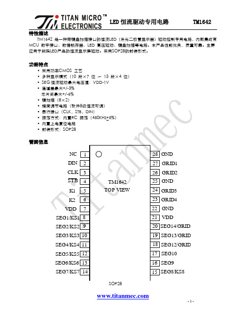
TM1642是一种带键盘扫描接口的恒流LED(发光二极管显示器)驱动控制专用电路,内部集成有MCU 数字接口、数据锁存器、LED 高压驱动、键盘扫描等电路。
本产品性能优良,质量可靠。
主要应用于段码LED产品的恒流显示屏驱动。
采用SOP28的封装形式。
功能特点•采用功率CMOS 工艺•多种显示模式(10段×7位~13段×4位)•SEG 恒流驱动最大电压值:VDD-1V •通道差最大+/-3%芯片间最大+/-6%•键扫描(8×2)•辉度调节电路(软件8级恒流可调)•串行接口(CLK,STB,DIN)•振荡方式:内置RC 振荡(450KHz+5%)•内置上电复位电路•封装形式:SOP28管脚信息123456789101112131415161718192021222324TM1642NCDINCLK STB K1K2VDDSEG1/KS1SEG2/KS2SEG3/KS3SEG4/KS4SEG5/KS5SEG6/KS6SEG7/KS7SEG8/KS8SEG9SEG10GRID1GRID2GRID3GRID4SEG14/GRID5SEG13/GRID SEG12/GRID VDD GND GND GND 25262728TOP VIEWSOP28深圳市富瑞世嘉科技有限公司13530167943天微专营为高时,CLK 被忽略输入该脚的数据在显示周期结束后被锁存段恒流输出(也用作键扫描),p管开漏输出16~17段恒流输出,P管开漏输出27、2624、23位输出,N管开漏输出输出(段/位)18~20段/位复用输出,只能选段或位输出逻辑电源7、215V±10%逻辑地22、25、28接系统地▲注意:DIN口输出数据时为N管开漏输出,在读键的时候需要外接1K-10K的上拉电阻,如图(1)所示。
本公司推荐10K的上拉电阻。
DOUT在时钟的下降沿控制N管的动作,此时读数不稳定,可以参考图(4),在时钟的上升沿时读数才稳定。
泉芯电子技木 高亮度LED灯升压驱动控制器 QX2305 说明书
高亮度LED灯升压驱动控制器 QX2305概述QX2305 是一款高效率,稳定可靠的高亮度LED灯驱动控制IC,内置高精度比较器,off-time控制电路,恒流驱动控制电路等,特别适合大功率,多个高亮度LED灯串恒流驱动。
QX2305采用固定off-time控制工作方式,其工作频率高达2.5MHz,可使外部电感和滤波电容、体积减少,效率提高。
off-time最小时间,可通过外部电阻和电感进行设置,工作频率根据用户要求而改变。
在EN端加PWM信号,可调节LED灯的亮度。
通过调节外置的电阻,能控制高亮度LED 灯的驱动电流,使LED灯亮度达到预期恒定亮度,流过高亮度LED灯的电流可从几毫安到1安培变化。
订货信息QX2305XLG:SO-8 特性y可编程驱动电流y高效率:最高达90%y宽输入电压范围:2V~400Vy高工作频率:>1.5MHzy工作频率可调:500KHz~1.5MHzy驱动LED灯功能强:LED灯串可从1个到几十个LED高亮度灯y亮度可调:通过EN端PWM,调节LED灯亮度应用范围y干电池供电LED灯串y LED灯杯y RGB大显屏高亮度LED灯y平板显示器LED背光灯y恒流充电器控制y通用恒流源方框图管脚排列图管脚定义:管脚序号管脚名称功能描述1 VSS电源地2 EN芯片使能端3 COMP内部比较器补偿4 FB电压反馈端5 DRV外部MOS驱动端6 CS电流反馈检测脚7 TOFF关断时间设定8 VDD电源正(2V-6.5V)极限参数参数符号描述值单位Vmax VDD脚电电压8 V 电压Vmin-max EN, CS 和 FB 脚电压值-0.3-VDD+0.3 VTmin-max 工作温度范围-20-85 o C 温度Tstorage 存储温度范围-40-165 o C ESD VESD ESD 电压(人体模式)2000 V主要电气性能和指标参数参数 符号测试条件最小 典型最大单位电源电压 VDD 2.56.5 VCS 脚反馈电压 V CS 240 250 260 MVFB 脚反馈电压 V FB970 1000 1030 MV工作电流IDD0.5 1 MA关断时间 (Toff 脚悬空) T OFF0640 ns待机电流 IDDQ1 uAEN 脚逻辑高电平 V ENH 2.0 VEN 脚逻辑低电平 V ENL 0.8 V DRV 脚电压上升时间T RISE500pF 电容在DRV 脚上时50 nsDRV 脚电压下降时间 T FALL 500pF 电容在DRV 脚上时50 ns应用指引QX2305是一款开关工作模式的大功率LED 驱动IC ,正常工作时给外部的电感充放电,通过反馈脚的反馈,可以得到恒定的输出电流。
最新LED恒流驱动芯片汇总
最新LED恒流驱动芯片汇总
LED恒流驱动芯片是一种用于控制LED灯工作电流的电子器件,它可
以帮助提高LED灯的亮度、节能和寿命。
随着LED照明技术的发展,LED
恒流驱动芯片也在不断更新和改进。
以下是一些最新的LED恒流驱动芯片
的汇总介绍。
1.NXPSSL5028GPH:NXPSSL5028GPH是一款数字式LED恒流驱动芯片,集成了多种电流选择和调节功能,可以实现精确的电流控制和亮度调节。
该芯片可广泛应用于室内和室外LED照明产品,具有高效、稳定和可靠的
特点。
2. STMicroelectronics L6924D:STMicroelectronics L6924D是一
款高性能LED驱动芯片,具有高达95%的转换效率。
该芯片采用恒流控制
和PWM调光技术,可以实现高亮度的LED照明效果。
同时,该芯片还具有
热保护和电压保护功能,有效保护LED灯的使用寿命。
4. Infineon ILD8150:Infineon ILD8150是一款集成式恒流驱动芯片,适用于室内和室外LED照明产品。
该芯片采用了新型的TRILINX技术,可以提供高效、低噪声和高稳定性的LED驱动效果。
同时,该芯片还具有
多种保护功能,如过温保护、短路保护和过电流保护等。
以上是一些最新的LED恒流驱动芯片的汇总介绍。
这些芯片具有高效、稳定和可靠的特点,可以实现精确的电流控制和亮度调节,满足不同应用
场景的LED照明需求。
随着LED技术的不断发展,LED恒流驱动芯片将继
续推陈出新,为LED照明市场带来更多创新和发展。
华旺光电子Warm White色顶LED单片机3528型号说明书

Factory : WAH WANG OPTOELECTRONIC (SHENZHEN) CO LTD.
Specification
For 3528 Single Chip Warm White Color Top LED Part No: WW-WRA30TS-U1
260( for 5 sec)
பைடு நூலகம்
℃
Electrical Optical Characteristics at Ta=25℃
Parameter
Symbol Min. Typ. Max. Unit
Test Condition
Luminous Intensity Ref. Luminous Flux
Viewing Angle
Iv1 2100 --- 3000 mcd
Φv1
7.5
8.5
---
lm
2θ1/2 --- 120 --- Deg
IF = 20mA(Note 10) IF = 20mA IF = 20mA
Forward Voltage
VF1
2.8
---
3.4
V
IF = 20mA
Luminous Intensity
Iv2 3000 --- 4000
Symbol
Value
Unit
Power dissipation
Pd
60
mW
Continuous Forward Current
IF
20
mA
Peak Forward Current (1/10 Duty Cycle, 0.1ms Pulse Width)
高功率LED驱动器MIC3230 1评测板说明书

1. Voltage source capable of supplying 50 Watts
2. Load: LED, resistive or electronic load
3. Scope
4. Voltage meter
5. (Optional) Function generator for PWM Dimming
The switching frequency is determined by the selection of R1. The chart in Figure 2 can be used to select the desired frequency. The board is set at approximately 500kHz.
How it works
The MIC3230/1 evaluation board is set to operate as a boost converter, which requires the output voltage to be greater than the input voltage. It is important to have the series LED forward voltage drops be greater than the input voltage because when the converter is off the input is connected to the output through the inductor (L1) and diode (D1). VIN is effectively applied across the LEDs and will turn on if the series sum of their forward voltage drop is not greater than VIN. For 100% duty cycle, simply pull PWMD high or leave open. For a different LED current change R7 using the following equation. When R7 is 0.62Ω, the LED current is equal to 0.4A. The evaluation board is currently set to this output current value.
BIT3252A
碩頡科技 管
BiTEK 制
May 16, 2007
DCC CONTROLLED
2007/04/26
Confidential, for authorized user onlypage 2 of 8
DOC NO.W-DS-0002
Beyond Innovation Technology Co., Ltd.
Beyond Innovation Technology Co., Ltd.
BIT3252A
BIT3252A
Low Cost PWM Controller built in 55V NMOS
Version: A2
Please read the notice stated in this preamble carefully before accessing any contents of the document attached. Admission of BiTEK’s statement therein is presumed once the 碩頡科技 BiTEK document is released to the receiver.
4
Absolute Ratings: (if Ta=25℃)
VDD…………………………...…………-0.3 ~ +8 V GND…………………..…………………±0.3 V Output Voltage……………….…….……-0.3 ~ 55 V Operating Ambient Temperature……….0 ~ 70 ℃ Extreme Operating Ambient Temp……-40 ~ 85 ℃ *** Operating Junction Temperature….….+150 ℃ Storage Temperature……………..…….-55~ 150 ℃
AP3126AP3127AP3127BAP3128AP3129AP3130高性能LED背光驱动器

AP3126AP3127AP3127BAP3128AP3129AP3130⾼性能LED背光驱动器⾼性能LED背光驱动器⾼性能背光动AP3126 1.2MHz,0.6A ⾼达20V微功率输出升压转换器AP3126是⼀款⼩功率应⽤的恒定频率、5脚SOT封装,电流模式升压转换器,AP3126的开关频率为1.2MHz,允许使⽤较⼩的低成本电容和2mm或更⼩⾼度的电感。
内部软启动减⼩浪涌电流,延长电池寿命。
AP3126的输⼊电压低⾄2.5V,5V输⼊可以提供20V ⾼达100mA电流。
AP3126在轻载时采⽤⾃动脉冲频率模式。
AP3126特性还包括电流限制和过流保护以防⽌输出过载时损坏芯⽚。
AP3126采⽤纤⼩的SOT-23-5L封装⼩的SOT-23-5L封装。
内置1.8Ω功率MOSFET 40mA静态电流 OLED偏置2.5V~5.5V输⼊电压 1.2MHz固定开关频率内部0.6A 开关限流 LCD偏置输⼊⽩光LED驱动 PDAs 数码相机可调输出电压内部补偿⾼达20V输出电压轻载⾃动脉冲频率调制超过85%效率采⽤SOT-23-5L封装AP3127升压型DC/DC LED 驱动器AP3127系列是固定振荡频率、恒流输出的升压型DC/DC转换器,⾮常适合于移动电话、PDA、数码相机等电⼦产品的背光驱动电路。
输出电压可达16V,3.2V输⼊电压可以驱动串联的四个LED,2.5V输⼊电压可以驱动两路并联LED(每路串联三个LED)。
通过改变CE脚上PWM信号的占空⽐可以控制LED的亮度。
内部集成有导通电阻只有1.8Ω的场效应管,外部可使⽤微型电感和电容,以缩⼩占⽤印制板的⾯积。
输⼊电压范围:2.5V⾄6.0V 输出电压范围:可达16V 启动参考基准电压:0.25V 振荡频率:10MHz ⽩光LED驱动移动电话机平板电脑振荡频率:1.0MHz 输出导通电阻:1.8Ω转换效率:88%(驱动三个串联LED@Vin=3.6V ILED=20mA) 通过PWM信号控制LED亮度待机电流ISTB 10A(MAX) 数码相机MP3,PMP,PDA待机电流:ISTB=1.0uA(MAX) 负载电容:0.22uF(瓷介) Lx最⼤电流:300mAAP3127B升压型DC/DC LED 驱动器AP3127B系列是固定振荡频率、恒流输出的升压型DC/DC转换器,⾮常适合于移动电话、PDA、数码相机等电⼦产品的背光驱动电路。
OB2532A Datasheet_CN_佛山照明_111209

定购信息 型号 OB2532AMP
备注: 芯片的实际应用条件超出规定的“应用极限值”将会 对芯片造成永久性损伤。以上应用极限值标志了芯片可承 受应力等级, 但并不建议芯片在此极限条件或超出“推荐工 作条件”下工作。 芯片长时间处于最大额定工作条件, 会影 响芯片的可靠性。
lt
o
佛
应用极限参数 Parameter VDD 电压 VDD 稳压管钳位电流 COMP 电压 CS 输入电压 INV 输入电压 最小/最大工作结温 TJ 最小/最大储藏温度 Tstg 管脚焊接温度(10secs)
佛
40 80 Temperature(℃)
山 照
120
明
OB2532A
高精度原边 PWM 电源开关器
工作原理概述
OB2532A 是一款低系统成本的 LED 驱动控制 器,芯片工作在不连续(DCM)模式,应用于反 激隔离 LED 照明。采用原边反馈控制技术,无 需 TL431 和光耦等二次侧元器件, 其内置专利的 恒流(CC)控制技术,可以实现高精度的 LED 恒流输出特性,满足 LED 照明应用。 启动电流和启动控制 OB2532A 优化设计了启动电流(Typ. 5uA) ,当 VDD 电压经充电高于 UVLO(OFF)阈值电压, 芯片可以很快开启工作,因此在系统板上可以使 用高阻值的启动电阻来减小功率损耗。 工作电流 OB2532A 低至 2mA 的工作电流和多模式控制方 式可以实现系统的高转换效率和低待机功耗。 软启动 系统上电后,OB2532A 的内部软启动功能可以 减小 LED 电流过冲, 当 VDD 电压经充电高于 UVLO(OFF)阈值电压,芯片内部算法控制 CS 引脚峰值电压逐渐从 0V 增加到 0.8V,每次重启 都有软启动。 CC 工作原理 OB2532A 专利的 CC 控制需要工作在不连续模 式,应用于反激隔离 LED 照明(参考第 1 页典型 应用图)。LED 输出电流 Iout 计算公式: TDemag 与原边绕组电感量成反比例,控制 Lp 和开 关频率的乘积恒定不变,这样输出电流就不随原边 电感量的变化而变化。 芯片最大补偿原边电感量± 7% 偏差变化,实现 LED 恒流输出。 LED 输出电流计算公式:
各种LED恒流驱动及恒流IC芯片盘点
各种LED恒流驱动及恒流IC芯片盘点LED恒流驱动简介山于LED是特性敬感的半导体器件,乂具有负温度特性,因而在应用过程中需要对其进行稳定工作状态和保护,从而产生了驱动的概念。
LED器件对驱动电源的要求近乎于苛刻, LED不像普通的白炽灯泡,可以直接连接220V的交流市电。
LED是2〜3伏的低电压驱动, 必须要设计复杂的变换电路,不同用途的LED灯,要配备不同的电源适配器。
国际市场上国外客户对LED驱动电源的效率转换、有效功率、恒流精度、电源寿命、电磁兼容的要求都非常高,设计一款好的电源必须要综合考虑这些因数,因为电源在整个灯具中的作用就好比像人的心脏一样重要。
LED驱动电源把电源供应转换为特定的电压电流以驱动LED发光的电压转换器,通常情况下:LED驱动电源的输入包括高压工频交流(即市电)、低压直流、高压直流、低压高频交流(如电子变压器的输出)等。
而LED驱动电源的输出则大多数为可随LED正向压降值变化而改变电压的恒定电流源。
LED电源核心元件包括开关控制器、电感器、开关元器件(MOSFET).反馈电阻、输入滤波器件、输出滤波器件等等。
根据不同场合要求、还要有输入过压保护电路、输入欠压保护电路,LED开路保护、过流保护等电路。
LED的恒流驱动用LED作为显示器或其他照明设备或背光源时,需要对其进行恒流驱动,主要原因是:1.避免驱动电流超出最大额定值,影响其可鼎性。
2.获得预期的亮度要求,并保证各个LED亮度、色度的一致性3.能有效的避免雷击,电网的浪涌,过电流,过电压的保护,使LED寿命提高。
存在问题:要处理好散热问题,散热问题没有处理好就会影响LED寿命。
口前LED均采用直流驱动,因此在市电与LED之间需要加一个电源适配器即LED驱动电源。
它的功能是把交流市电转换成合适LED的直流电。
根据电网的用电规则和LED的驱动特性要求,在选择和设计LED驱动电源时要考虑到以下儿点:1•高可鼎性特别像LED路灯的驱动电源,装在高空,维修不方便,维修的花费也大。
FM7222DS-3W LED功率射灯驱动IC 可替换BP9022A

产品概述FM7222DS是高精度原边反馈的LED恒流驱动芯片。
芯片工作在电感电流断续模式,适用于85Vac~265Vac全范围输入电压、反激式隔离LED恒流电源。
FM7222DS芯片内部集成650V功率开关,采用原边反馈模式,无需次级反馈电路,也无需补偿电路,只需要极少的外围元件即可实现恒流。
采用专利的驱动和电流检测方式,芯片的工作电流极低,无需变压器辅助绕组检测和供电,进一步减少外围元器件,极大的节约了系统成本和体积。
FM7222DS芯片内带有高精度的电流取样电路,使得LED输出电流精度达到±5%以内。
芯片采用了特有的恒流控制方式,可以达到优异的线性调整率。
FM7222DS具有多重保护功能,包括LED开路/短路保护,欠压保护,芯片过温保护等。
特性➢内部集成650V功率管;➢原边反馈恒流控制,无需次级反馈电路;➢无需变压器辅助绕组检测和供电;➢芯片超低工作电流;➢宽输入电压;➢±5% LED 输出电流精度;➢LED短路/开路保护;➢芯片供电欠压保护;➢过温保护;➢封装形式:SOP-8 。
应用范围➢LED射灯;➢LED 球泡灯;➢其它LED照明。
内部框图流和交流电参数规范。
对于未给定上下限值的参数,该规范不予保证其精度,但其典型值合理反映了器件性能。
注2:温度升高最大功耗一定会减小,这也是由TJMAX, θJA,和环境温度TA所决定的。
最大允许功耗为PDMAX (TJMAX - TA)/ θJA或是极限范围给出的数字中比较低的那个值。
推荐工作范围电气特性应用信息FM7222DS是一款专用于LED照明的恒流驱动芯片,采用专有的恒流架构和控制方法,芯片内部集成650V功率开关,只需要极少的外围组件就可以达到优异的恒流特性。
采用了原边反馈技术,FM7222DS无需光耦及TL431反馈,也无需辅助绕组供电和检测,系统成本极低。
启动系统上电后,母线电压通过启动电阻对V CC电容充电,当V CC电压达到芯片开启阈值时,芯片内部控制电路开始工作。
led灯pwm调光电路芯片

led灯pwm调光电路芯片
LED灯的PWM调光电路芯片是用来控制LED灯的亮度的关键元件。
PWM(脉冲宽度调制)调光是一种常见的LED调光方法,通过控制LED的通电时间来实现亮度的调节。
以下是一些常见的用于LED 灯PWM调光的电路芯片:
1. 555定时器芯片,555定时器是一种常用的集成电路,可以被用于产生PWM信号。
它可以被配置成单稳态或者多谐振荡器,用来产生PWM信号以控制LED的亮度。
2. 专用LED驱动芯片,一些厂商生产了专门用于LED灯PWM调光的驱动芯片,例如TI的TLC5940等。
这些芯片通常集成了PWM调光控制电路和LED驱动电路,能够提供更精确和稳定的调光效果。
3. 微控制器,一些带有PWM输出引脚的微控制器也可以用来控制LED的亮度。
通过编程,可以实现各种复杂的PWM调光算法,以满足不同的应用需求。
4. 电容和电阻,除了使用专门的芯片外,一些简单的LED调光电路也可以通过电容和电阻来实现PWM调光。
这种方法成本低廉,
但通常只适用于简单的应用场景。
总的来说,选择合适的LED灯PWM调光电路芯片取决于应用的需求,包括亮度调节范围、精度要求、成本考虑等因素。
在选择时需要综合考虑这些因素,以找到最适合的解决方案。
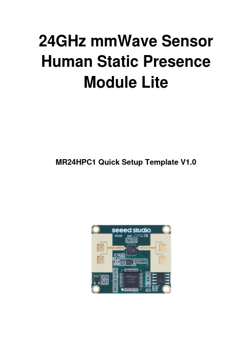
浩盛科技 MR24HPC1 产品说明书
24GHz mmWave Sensor Human Static PresenceModule LiteMR24HPC1 Quick Setup Template V1.0Catalog1.Overview (2)2.Parameter Setting Template Under Standard Mode (2)2.1Bathroom Scene (2)2.2Bedroom Scene (3)2.3Office/Conference Room Scene (3)3.Custom Mode Parameter Settings Template (4)3.1Bathroom (5)3.2Bedroom (6)3.3Office/Conference Room (7)3.4Warehouse and Logistics (8)1. OverviewFor several common application scenarios in real life, the following provides some commonly used settings experience values for reference. When using them for the first time, you can set them based on the reference values. If the effect is not good, you can flexibly adjust them based on the parameter introduction in the User Manual.This template will be divided into two parts: one is the parameter setting under Standard mode, and the other is the parameter setting under Custom mode. For the vast majority of users, the standard mode functions are sufficient. We recommend that you first try using the standard mode, and if the desired effect cannot be achieved, consider using the custom mode.Under custom mode, the parameter settings require the user to send a command to the radar to enable the custom mode function before they can be set. After sending the command to end the setting to the radar, it should be saved and take effect.2. Parameter Setting Template UnderStandard Mode2.1 Bathroom SceneEnvironmental description: The room area is between 3.5 ~ 6 ㎡. There are facilities such as a washbasin, glass door, exhaust fan, and toilet in the room. The source of interference in the room is the exhaust fan.Sensor installation suggestion: Install it at the top in the middle of the bathroom.Setting Template: Select “Bathroom Mode” for scene mode and set sensitivity to “1”.The format of the command to be sent is (in hexadecimal):53 59 05 07 00 01 03 BC 54 4353 59 05 08 00 01 01 BB 54 43Reason: Due to the small size of the bathroom, the bathroom mode with sensitivity 1can be selected (the radar wave cannot penetrate solid walls, but can penetrate glass, partition walls, etc.). The radar should be at least 0.5m away from the exhaust fan.2.2 Bedroom SceneEnvironmental description: The room is approximately 20 ㎡in size and contains facilities such as air conditioning, fans, and a bed. Interference sources in the room include air conditioning and fans. The radar cannot accurately distinguish between humans and pets, so pets may also interfere with the normal detection of the radar.Sensor installation suggestion: It is recommended to install the radar at a central position in the bedroom, preferably slightly closer to the bed to ensure coverage of the sleeping area.Setting Template: Select “Area Detection Mode” for scene mode and set sensitivity to “2”.The format of the command to be sent is (in hexadecimal):53 59 05 07 00 01 04 BD 54 4353 59 05 08 00 01 02 BC 54 43Reason: If the dynamic detection range is too large/small, you can correspondingly set the Bathroom/Bedroom Mode. If the static detection range is too large/small, you can correspondingly set sensitivity 1/sensitivity 3. (Radar waves cannot penetrate solid walls, but can penetrate glass, partition walls, etc.)If it is not possible to exclude interference sources such as air conditioners and fans from the detection range, the air conditioners, fans, and other devices must be turned off so that the radar can enter an Unoccupied state.2.3 Office/Conference Room SceneEnvironmental description: The room has an area of approximately 35 ㎡and is equipped with central air conditioning, curtains, and a desk. The sources of interference inthe room are the central air conditioning and the curtains.Sensor installation suggestion: It is recommended to install it at the top or a tilted position in the center of the room, while keeping a distance of at least 0.5m between the radar and the exhaust fan.Setting Template: Select “Bedroom Mode” for scene mode and set sensitivity to “3”.The format of the command to be sent is (in hexadecimal):53 59 05 07 00 01 02 BB 54 4353 59 05 08 00 01 03 BD 54 43Reason: If the dynamic detection range is too large/small, you can set the Area Detection/Living Room Mode accordingly. If the static detection range is too large, you can set the sensitivity to 2. (Radar waves cannot penetrate solid walls, but can penetrate glass and partition walls, etc.)Note that you need to consider the impact of wind on the curtains. If the curtains are within the radar detection range, you can reduce interference by changing the installation position or reducing the scene mode/sensitivity.3. Custom Mode Parameter SettingsTemplateIf you want to set the following parameters, please use the command in the table below to enter custom mode.3.1 BathroomThe environmental interference factors that cannot be controlled by the standard mode include: In the Bathroom Scene, there may be facilities such as exhaust fans, glass doors, and curtains, and the potential sources of interference may include slight vibrations caused by the exhaust fan or slight swinging of metal rings on the curtain.Sensor installation suggestion: Suggested installation is to place the radar sensor at the top and center of the bathroom and slightly away from the exhaust fan to reduce interference.Setting suggestion:3.2 BedroomThe environmental interference factors that cannot be controlled by the standard mode include: In the scenario of a bedroom at home, there may be facilities such as air conditioners, fans, and floor cleaning robots, as well as pets such as cats and birds. Interference sources may exist, such as the operation of fans, air conditioners, and floor cleaning robots. Radar cannot accurately distinguish between humans and pets, so pets may also become interference sources and cause false alarms for the radar.Sensor installation suggestion: It is recommended to install the radar at the center of the ceiling and ensure that the air conditioner is not within the detection range of the radar.Setting suggestion:3.3 Office/Conference RoomThe environmental interference factors that cannot be controlled by the standard mode include: In an office setting, there may be glass walls, central air conditioning, curtains, and other facilities in the office/meeting rooms. The interference sources may include slight vibrations caused by central air conditioning, the metal plates swinging due to the curtains, or people walking outside the glass walls.Sensor installation suggestion: It is recommended to install the radar at the top or tilt it slightly and place it away from the central air conditioning unit.Setting suggestion:3.4 Warehouse and LogisticsThe environmental interference factors that cannot be controlled by the standard mode include: In the scenario of warehousing and logistics, the primary practical application is to trigger the function. The stationary metal storage shelves will not interfere with the radar's detection performance, while moving loading and unloading forklifts and pedestrian traffic can trigger the radar to detect the presence of people as usual.Sensor installation suggestion: It is recommended to install the radar at the top in the scenario of warehousing and logistics.Setting suggestion:。
MP3336A-C-00A双通道高功率闪光LED驱动器说明书

EV3336A-C-00ADual-Channel Flash LED DriverWith 2A/Ch and I2C InterfaceDESCRIPTIONThe MP3336A is a compact, dual-channel, high-power, flash LED driver that can drive up to 2A in flash mode for each LED. It is usually applied for camera phones to improve image and video quality in low-light environments. The MP3336A operates with a selectable 1/2/3/4MHz switching frequency and uses a synchronous, current-mode PWM boost converter to regulate the LED current with two high-current sources. The MP3336A provides a high efficiency and optimized solutionfor smaller PCB spaces.The MP3336A features a standard I2C interface, dual LED channels, rich protection modes, and high power density and performances. The MP3336A can also support flash, assist, indicator, and 5V DC modes.The cathodes of the dual-flash LED are referenced to GND, which is better for improving thermal performance in layout. The MP3336A is available in a WLCSP-20 (1.6mmx2.0mm) package.ELECTRICAL SPECIFICATION Parameter SymbolValueUnits Input Voltage V IN 2.7-5.5 V Output Voltage V OUT <5.5 VLEDs # 2LED Current/string I LED Max.2 A FEATURES∙ 2.7V~5.5V Input Voltage∙1/2/3/4MHz Selectable Max Fsw∙Fsw Fold-back Function∙ 400kHz I2C Compatible Interface∙ Standby/Flash/Assist/Indicator/5V DC ModesFlash Mode∙Up to 2A/Ch Programmable Current with ±7% Accuracy for Each LED, 7.84mA/Step Assist Mode∙Up to 319mA/Ch Programmable Current with ±7% Accuracy for Each LED,1.25mA/StepIndicator Mode∙Works in 31.5kHz PWM Dimming Mode with 2/16, 3/16, 4/16, 5/16 Duty Cycle∙Used for Blinking and 128/256/512ms Selectable Blinking Time5V DC Mode∙Output Constant 5V DC Voltage∙Separated EN1 Pin for NFC Application∙1A to 4.2A Programmable Input DC Current Limit Protection∙External Strobe/TX Pin∙VIN to VOUT Disconnection Function∙Low-Battery Voltage Protection∙LED Short/Open Protection∙VOUT-GND Short Protection∙Over-Voltage Protection (OVP)∙Over-Temperature Protection (OTP)∙Input Under-Voltage Lockout (UVLO) Protection∙ WLCSP-20 (1.6mmx2.0mm) Package APPLICATIONS∙Smartphone Flash LED Application∙Cameras for Tablets∙ Digital Still CameraAll MPS parts are lead-free, halogen free, and adhere to the RoHS directive. For MPS green status, please visit MPS website under Quality Assurance. “MPS” and “The Future of Analog IC Technology” are Registered Trademarks of Monolithic Power Systems, Inc.EV3336A-C-00A EVALUATION BOARD(L × W) 5.5cm x 5.5cmBoard Number MPS IC NumberEV3336A-C-00A MP3336AGCEVALUATION BOARD SCHEMATICFigure 1: Dual-Channel Application CircuitEV3336A-C-00A BILL OF MATERIALSQty Ref Value Description Package Manufacturer Manufacturer PN 1 C1 NC 06032 C2,C4 10uFCeramicCapacitor,10V,X5R0805 muRata GRM21BR61A106KE19L 1 C3 NC 0805 3 R1,R6,R7 0 res,1% 0603 Yageo RC0603FR-070RL 4 R2,R3,R4,R5 NC 0603 1 L1 1.1uH 1.1uA, 20m, 3.46A TDK D53LC-#A915AY-1R1M1 U1 MP3336A CSP92.01*1.61mmMPS MP3336APRINTED CIRCUIT BOARD LAYQUICK START GUIDE1. Connect the positive and negative terminals of the power supply (2.7V ~5.5V) to the VIN and GNDpins on the EV board, respectively.2. Supply the EN terminal with logical signal.3. Connect the positive and negative terminals of the LED to the LED1/2 pin and GND on the EVboard, respectively.4. Please connect SCL, SDA and GND of EV board to the SCL, SDA and GND of a programmable kit(EVKT-USBI2C-02) with I2C interface, respectively.5. Power on sequence: VIN →EN →I2C setting → Set LED1/2_EN bit (to light the LED load). Whenwork in flash mode with hardware trigger mode, please give a level or pulse signal to STR pin. NOTICE: The information in this document is subject to change without notice. Users should warrant and guarantee that third party Intellectual Property rights are not infringed upon when integrating MPS products into any application. MPS will not assume any legal responsibility for any said applications.。
HM6282内置MOS升压型大功率LED恒流驱动器典型应用电路图

参数 输入电压 芯片电源电压 系统工作频率
符号 VIN VDD FOP
最小值
典型值
最大值 50
单位 V V KHz
4.5
6.8
7 1000
3 of 5
HM6282 内置 MOS 升压型大功率 LED 恒流驱动器
调光频率 FPWM 250 1000 Hz
注 2:推荐工作范围是指在该范围内,器件功能正常,但并不完全保证满足个别性能指标。
5 of 5
HM6282 内置 MOS 升压型大功率 LED 恒流驱动器
封装信息
SOP14 封装参数
6 of 5
EN 使能端输入
EN 端输入高电平 EN 端输入低电平 大于 1.1V 无效 0.9 1.0 1.1 0.2 V V
低电平有效
典型升压豪华型应用电路(可设定恒流和恒压输出。带输入欠压保护功能和空载保护)
图 1:VIN=12~24VDC VOUT=38V.IOUT=0.65A 典型升压
经济型应用电路图 3(恒流精度为±3%.空载保护)
温度保护
温度 130 PC
o
短路保护
工作电流 IN:12VDC 0.8 mA
内置功率 MOS 管
最大漏源电压 导通内阻 MOS 管导通阈值 VDS_MAX RDS(ON) VTH VGS=4.5V , ID=8A 1 60 48 2.5 V mΩ V
4 of 5
HM6282 内置 MOS 升压型大功率 LED 恒流驱动器
电气特性 除非特别说明,VDD=5.6V,TA=25oC
参数
符号
测试条件 电源电压
最小值
典型值
最大值
单位
最大输入电压 欠压保护电压
33522a技术指标
33522a技术指标
1.波形生成:
•1mHz-30MHz的正弦波输出频率范围,1mHz分辨率。
•标配TCXO温度补偿晶体振荡器,OCXO高稳时基选件提供超高稳定度。
•<40ps的抖动,低于0.04%的总谐波失真,适用于精度更高的信号。
•幅度范围为1mVpp至10Vpp,1mV分辨率。
•标准波形:正弦波、方波、斜波、三角波、脉冲、噪声、PRBS伪随机序列、直流电压。
•内置任意波形:指数上升和下降、心率波、高斯脉冲、半正弦、负斜波、Lorentz、SinC。
•16Bit分辨率,250MSa/s采样率,标配1M点(选件16M)的任意波形。
•内置的任意波形产生和编辑器。
•更为强大的Arb任意波形编辑软件选件。
•标配提供AM、FM、PM、FSK、PWM、BPSK、SUM(载波+调制)调制功能。
•工作模式:连续、调制、扫频、突波、输出门。
2.仪器特性:
•大的彩色图形化显示界面易于信号设置和验证。
LTC3252 快速入门指南说明书
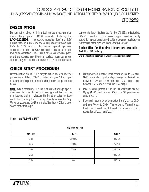
QUICK START GUIDE FOR DEMONSTRATION CIRCUIT 611 DUAL, SPREAD-SPECTRUM, LOW NOISE, INDUCTORLESS STEP DOWN DC/DC CONVERTERLTC3252 DESCRIPTIONDemonstration circuit 611 is a dual, spread-spectrum, step down charge pump DC/DC converter featuring the LTC®3252EDE. It produces regulated 1.5V and 1.2V output voltages at up to 250mA of output current each from 2.7V to 5.5V input. The unique spread spectrum architecture of the LTC3252 provides highly efficient and low noise operation. The circuit has a low external parts count and requires only five small surface mount capacitors and four tiny surface mount resistors. DC611 demonstrates appropriate layout techniques for the LTC3252 inductorless DC-DC converter. This power supply circuit is ideally suited for space-constrained battery-powered applications that require small size and low operating current.Design files for this cir cuit boar d ar e available. Call the LTC factory.LTC is a registered trademark of Linear Technology Corporation.QUICK START PROCEDUREDemonstration circuit 611 is easy to set up and evaluate the performance of the LTC3252. Refer to Figure 1 for proper measurement equipment setup and follow the procedure below:NOTE:When measuring the input or output voltage ripple, care must be taken to avoid a long ground lead on the oscilloscope probe. Measure the input or output voltage ripple by touching the probe tip directly across the V IN, V OUT1 or V OUT2 and GND terminals. See Figure 2 for proper scope probe technique. 1.With power off, connect input power source to V IN andGND terminals. Input voltage range is limited to between 2.7V and 5.5V for the 1.2V output and between 3.21V and 5.5V for the 1.5V output.2.Place selector jumper JP1 in the ON position to enableV OUT1 (1.5V), and jumper JP2 in the O N position to enable V OUT2.3.If desired, loads may be connected from V OUT1 to GNDand from V OUT2 to GND. The following V IN (min) vs.load chart must be followed to ensure correct regulation of V OUT1 and V OUT2:Table 1.V IN VS. LOAD CHARTV IN (min) vs loadV IN (MIN) I OUT1I OUT23.5V 250mA 250mA3.2V 100mA 250mA3.1V 50mA 250mA2.9V --- 250mA2.7V --- 150mAQUICK START GUIDE FOR DEMONSTRATION CIRCUIT 611DUAL, SPREAD-SPECTRUM, LOW NOISE, INDUCTORLESS STEP DOWN DC/DC CONVERTERNOTE: V OUT1 is in dropout for V IN < 3.0V and will cause theLTC3252 to operate in continuous mode instead of the more efficient burst mode. To monitor the actual performance of V OUT2 for V IN <3.1V, V OUT1 should be disabled by placing jumper JP1 in the OFF position.4. Turn on the power at the input.NOTE: Make sure that the input voltage does not exceed5.5V.5. Check for the proper output voltages. V OUT1 = 1.5V andV OUT2 = 1.2V. If there is no output, temporarily disconnect the load to make sure that the load is not set too high. 6. Once the proper output voltages are established, adjust the loads up to 250mA and observe the output voltage regulation, input and output ripple voltage, efficiency and other parameters. Remember to follow the V IN (min) vs. load chart for correct regulation of V OUT1 and V OUT2.Figure 1. Proper Measurement Equipment SetupFigure 2.Scope Probe Placement for Measuring Input or Output RippleQUICK START GUIDE FOR DEMONSTRATION CIRCUIT 611 DUAL, SPREAD-SPECTRUM, LOW NOISE, INDUCTORLESS STEP DOWN DC/DC CONVERTER。
- 1、下载文档前请自行甄别文档内容的完整性,平台不提供额外的编辑、内容补充、找答案等附加服务。
- 2、"仅部分预览"的文档,不可在线预览部分如存在完整性等问题,可反馈申请退款(可完整预览的文档不适用该条件!)。
- 3、如文档侵犯您的权益,请联系客服反馈,我们会尽快为您处理(人工客服工作时间:9:00-18:30)。
BIT3252A
Low Cost PWM Controller
built in
55V NMOS
Version: A2
Please read the notice stated in this preamble carefully before accessing any contents of the document attached.
Admission of BiTEK’s statement therein is presumed once the document is released to the receiver.
Notice:
Firstly, the information furnished by Beyond Innovation Technology Co. Ltd. (BiTEK) in this document is believed to be accurate and reliable and subject to BiTEK’s amendment without prior notice. And the aforesaid information does not form any part or parts of any quotation or contract between BiTEK and the information receiver.
Further, no responsibility is assumed for the usage of the aforesaid information. BiTEK makes no representation that the interconnect of its circuits as described herein will not infringe on exiting or future patent rights, nor do the descriptions contained herein imply the granting of licenses to make, use or sell equipment constructed in accordance therewith.
Besides, the product in this document is not designed for use in life support appliances, devices, or systems where malfunction of this product can reasonably be expected to result in personal injury. BiTEK customers’ using or selling this product for use in such applications shall do so at their own risk and agree to fully indemnify BiTEK for any damage resulting from such improper use or sale.
At last, the information furnished in this document is the property of BiTEK and shall be treated as highly confidentiality; any kind of distribution, disclosure, copying, transformation or use of whole or parts of this document without duly authorization from BiTEK by prior written consent is strictly prohibited. The receiver shall fully compensate BiTEK without any reservation for any losses thereof due to its violation of BiTEK’s confidential request. The receiver is deemed to agree on BiTEK’s confidential request therein suppose that said receiver receives this document without making any expressly opposition. In the condition that aforesaid opposition is made, the receiver shall return this document to BiTEK immediately without any delay. -Version A4
y Array y y y y y y y y
y
Layout Notice:
Some of the pins are very sensitive to noise. Please follow the bellowing guideline to make the layout:
Soldering Information
Reflow Soldering:
The choice of heating method may be influenced by plastic QFP package). If infrared or vapor phase heating is used and the package is not absolutely dry (less than 0.1% moisture content by weight), vaporization of the small
≧
Unit: mm SOP type :。