Slotantenna缝隙天线设计
一种小型宽频带缝隙天线的设计

一种小型宽频带缝隙天线的设计作者:王代华韩峰来源:《现代电子技术》2019年第03期关键词:缝隙天线; 宽频带; Ansoft HFSS; 模型仿真; 结构优化; 无线通信中图分类号: TN822+.8⁃34 ; ; ; ; ; ; ; ; ; ; ; ; 文献标识码: A ; ; ; ; ; ; ; ; ; ; ; 文章编号:1004⁃373X(2019)03⁃0031⁃04Abstract: A novel compact minitype broadband microstrip antenna working in 10 GHz broadband is designed, which takes FR4 with the size of 24 mm×23 mm×1.6 mm as its substrate. A slot composed of regular hexagon and symmetrical cross type patches is designed in the center location of substrate ground plane to enlarge the working bandwidth. The microstrip line is located in the opposite side of the substrate. The electromagnetic simulation software Ansoft HFSS is used to perform the model simulation and structure optimization for the antenna. The antenna was processed and tested. The results show that the working bandwidth of the antenna covers the range of 3.6~13.6 GHz, the impedance bandwidth can reach up to 116%, and the antenna has perfect radiation characteristic in the frequency band. The reflection loss curves and radiation pattern are given. The test results are basically the same with simulation results. The design provides a certain reference for the study on broadband wireless communication.Keywords: slot antenna; broadband; Ansoft HFSS; model simulation; structure optimization; wireless communication小型縫隙天线在雷达、遥测与移动通信等领域扮演着重要角色。
一种高性能波导缝隙阵列天线的设计

图1 可快速迭代的波导阵列天线设计方法步骤一:从天线的指标出发(波束宽度、副瓣水平、波束指向等),通过天线综合的方法获得所需的口经场幅度、相位分布,典型的综合方法如泰勒综合法、切比雪夫综合法、伍德沃德加权综合法等。
此过程还依赖于天线的近远场转换技术,可在天线形式已知的情况下实现口径场与远场的相互转换,是一项关键的技术。
步骤二:利用口径场求解缝隙电导分布。
此过程的实现依赖于微波网络的分析技术,涉及多端口网络参数的相互转化,如根据口径场分布进而得到缝隙处的散射场(S参数),由S参数与导纳矩阵Y之间的转换关系,进而得到缝隙电导分布。
步骤三:通过获得的缝隙电导分布,确定每个缝隙的电图2 缝隙导纳分布波导缝隙的阻抗特性是决定天线阵单个阵元特性最为重要的特性。
确定缝隙阵列所需的导纳分布后,便要获得缝隙导纳与其电尺寸的对应关系,经拟合的缝隙倾角与归一化导纳之间的对应关系如图3所示。
另外,缝隙的切深可由谐振频率等因素确定。
图3 缝隙谐振时倾角与电导的拟合曲线本文设计中采用标准矩形波导BJ-100,内部尺寸22.86mm*10.16mm,波导壁厚为1.72mm。
设计由226元缝隙构成的天线阵,相邻缝隙间等间距分布、交替导向。
考虑到扫描角度、带宽、功率容量等因素,设定缝隙间距为 (a) 天线侧视图 (b)天线俯视图 (c)缝隙波导天线 (d)天线结构和尺寸图4 天线形式图4 高性能波导缝隙阵列天线测试结果采用XD-II型天线近远场天线测量系统,对阵列天线进行测试。
测试件数量为3个X波段雷达天线。
测试内容包括天线方向图、天线增益、天线电压驻波比。
测试方法如下。
(1)天线方向图。
在微波暗室内采用平面近场扫描方法,进行天线方向图测试。
被测天线为发射天线,探头接收发射信号。
将天线架设在转台上,调整天线的方位面和俯仰面,确定天线辐射阵面与探头扫描面保持平行。
天线架设及调平完毕以后,启用平面近(远)场测量测试软件,设置近(远)场平面测试系统测试参数,进行测试并自动记录,保存被测天线近场采集数据。
基于ADS的微带天线的设计与仿真设计
基于ADS的微带天线的设计与仿真The design and simulation of PIFA based on ADS 王伟堃(Wang Weikun)06250109计算机与通信学院本科生毕业设计说明书基于ADS的微带天线的设计与仿真作者:王伟堃学号:06250109专业:通信工程班级:06级通信工程(1)班指导教师:侯亮答辩时间:2010年6月15日平面倒F天线(PIFA,Planar Inverted F Antenna)主要应用在手机终端中,由于其体积小、重量轻、成本低、性能好,符合当前无线终端对天线的要求,因而得到广泛的应用,进行了许多研究工作。
先进设计系统(Advanced Design System),简称ADS,是安捷伦科技(Agilent)为适应竞争形势,为了高效的进行产品研发生产,而设计开发的一款EDA软件。
软件迅速成为工业设计领域EDA软件的佼佼者,因其强大的功能、丰富的模板支持和高效准确的仿真能力(尤其在射频微波领域),而得到了广大IC设计工作者的支持。
ADS可以模拟整个信号通路,完成从电路到系统的各级仿真。
它把广泛的经过验证的射频、混合信号和电磁设计工具集成到一个灵活的环境中,包括从原理图到PCB 板图的各级仿真,当任何一级仿真结果不理想时,都可以回到原理图中重新进行优化,并进行再次仿真,直到仿真结果满意为止,保证了实际电路与仿真电路的一致性。
本设计通过ADS软件对微带天线进行设计,设计了平面倒F天线,即PIFA天线的设计以与利用Hilbert分型结构对天线小型化设计。
论文主要包括:PIFA天线的介绍,ADS软件的使用,PIFA天线的设计以与仿真,优化与结果分析等容。
论文结构安排如下:第一章绪论;第二章FIFA天线原理与介绍;第三章ADS软件的使用;第四章PIFA天线的设计;第五章仿真优化与结果分析。
第一章介绍了本设计要解决的问题,提出了用ADS软件设计PIFA天线。
新式凹槽形缝隙超宽带微带天线的设计
凹槽形的半圆边长
微带线的长度
式中:f 为凹槽形缝隙天线的谐振频率ꎬc 为真空中
微带线的宽度
光速ꎬε r 为介质基板的相对介电常数ꎬL 为缝隙的边
微带线与基板左侧的距离
长ꎮ 此外ꎬ微带馈电线的阻抗对于天线阻抗匹配也
缝隙的横向尺寸
有一定的的影响ꎬ一般为 50 Ω 最合适ꎬ其尺寸计算
公式如下所示:
L2
43
d2
L1
d3
5.4
15
32
2 参数分析
2.1 凹槽形缝隙边长 L 0 对阻抗带宽的影响
分别选取 L 0 = 42 mmꎬL 0 = 43 mm 以及 L 0 = 44
mm 这三种不同情况对天线进行仿真分析ꎮ 由图 2
可以得到ꎬ随着 L 0 的增大ꎬ天线的谐振频率几乎不
598
第 44 卷
Abstract:A new type of groove ̄shaped slot ultra ̄wideband ( UWB) microstrip antenna is designed for the narrow
bandwidth of narrow ̄band microstrip slot antenna. The microstrip line is used to excite the groove ̄shaped slit method
调整的尺寸参数更多ꎬ故更容易实现阻抗匹配ꎮ
该天线的最低谐振频率可以通过改变凹槽形缝
隙的尺寸大小来调整ꎮ 凹槽形缝隙天线的最低谐振
频率可以通过下面的多边形缝隙天线公式得到:
f=
c
L εr
(1)
优化目标得到ꎬ具体的天线尺寸参数在表 1 中给出ꎮ
波导缝隙阵仿真设计_毕业设计论文 精品

学校代码:_ 11059_学号:0905072010Hefei University毕业论文(设计)BACH ELOR DISSERTATION论文题目:__________波导缝隙阵仿真设计____ ____学位类别:工学学士学科专业:________________ 通信工程作者姓名:_______________ 马跃_____________ _________导师姓名:郑娟完成时间:_________ 2013-5-27_________ _波导缝隙阵仿真设计中文摘要缝隙天线是由金属面上的缝隙构成的天线。
波导裂缝阵列天线由于其体积小、重量轻、口径效率高、功率容量大和容易实现低副瓣及超低副瓣等优点,在机载火控雷达、导弹导引头等方面有着极为广泛的应用。
波导上的缝隙随着其切割位置的不同构成了不同形式的缝隙。
经常使用的缝隙有开在波导窄边的倾斜缝隙,开在波导宽边的纵向缝隙、横向缝隙以及开在波导宽边中心线上到倾斜缝隙,它们既可以是谐振式的,也可以是非谐振式的。
由于这些缝隙均切割表面电流,因而将向外部空间辐射能量,对这些缝隙的个数、位置、尺寸、排列进行精心选择,就能产生各种实用的天线。
本次设计要求为天线中心频率10GHz。
本设计通过理论计算和软件仿真实现相结合最终得出结果,最后结果从方向图可以看出该缝隙的增益达到19.05dB,且呈现笔形波束。
而第一副瓣约为-9.5dB,与主瓣相差28.55dB左右,满足波导缝隙阵天线使用场合的低副瓣要求。
关键词:波导缝隙阵;阻抗;导纳;散射系数;HFSS;泰勒线源Design of Waveguide Slot Array SimulationABSTRACTThe slot antenna is the antenna consists of metal surface of the gap. Waveguide slot array antenna because of its small size, light weight, high aperture efficiency,large power capacity and easy to realize low sidelobe and ultra low sidelobe and other advantages, has been widely used in airborne fire control radar, missile seeker. Slot waveguide with the cutting position of different form the gap. Gap are often used in the inclined slot waveguide edge, opened in the longitudinal slot waveguide, the transverse slot and open to the inclined slot in the waveguide center line, they can be resonant, also can be the non resonant. Because of these gaps are cutting surface current, thus to outer space radiation energy, the slot number, location, size, arrangement of carefully selected, can produce a variety of antenna .The design requirements for the antenna center frequency 10GHz. This design through theoretical calculation and software simulation to achieve the combination of the final results, the final results from the direction of the gap can be seen that gain reaches 19.05dB, and presented a pencil beam. And the first sidelobe is about -9.5dB, and the main valve is about28.55dB, meet the waveguide slot array antenna used low sidelobe requirements.KEY WORD: waveguide slot array; impedance; admittance; scattering coefficient; HFSS; Taylor line source目录第一章前言 (1)1.1 波导缝隙阵天线研究背景及意义 (1)1.2 波导缝隙阵研究的现状 (2)第二章波导缝隙阵天线概述 (4)2.1 天线简介 (4)2.2 波导缝隙阵概述 (5)2.3 波导裂缝阵天线的组成 (5)2.3.1辐射阵面 (5)2.3.2耦合波导 (6)2.3.3馈电波导 (6)2.4 缝隙类型 (7)2.4.1 缝隙类型简介 (7)2.4.2 宽边纵向半波谐振缝隙 (8)2.4.3 宽边横向半波谐振缝隙 (8)2.4.4 窄边斜半波谐振缝隙 (9)2.5 典型波导缝隙阵天线介绍 (9)2.5.1为开在宽壁上的横向谐振缝隙阵 (9)2.5.2 纵向谐振缝隙阵 (10)2.5.3 纵向谐振缝隙阵二 (10)2.5.4非谐振式缝隙阵 (11)2.5.5 匹配偏斜缝隙阵 (11)2.6 缝隙阵列天线参数确定 (12)2.6.1波导缝隙尺寸的确定 (12)2.6.2 波导尺寸和阵元间距的确定 (12)2.6.3泰勒线源近似 (13)2.6.4波导缝隙阵长及缝隙数目的确定 (14)2.6.5辐射缝隙的电导值的确定 (15)2.6.6缝隙偏移量的确定 (15)2.6.7 缝隙匹配的电导条件 (15)第三章技术实现 (16)3.1 软件简介 (16)3.2 天线的技术实现及大体结构 (16)3.2.1 设计原理 (16)3.2.2 HFSS软件的仿真实现 (18)第四章波导缝隙阵的仿真设计过程 (19)4.1 仿真过程 (19)4.1.1子工程1:给定缝隙偏移,优化缝隙的谐振长度 (19)4.1.2子工程2:所有缝隙的完整模型 (23)4.2 天线性能 (27)第五章结论 (28)参考文献 (29)致谢 (30)第一章前言1.1 波导缝隙阵天线研究背景及意义缝隙天线是由金属面上的缝隙构成的天线。
PIFA天线的仿真设计

本科毕业论文(设计)题目:平面倒F缝隙天线的仿真分析学院:自动化工程学院专业:通信工程姓名:杜哲指导教师:宗卫华2010年5月30日Simulation Analysis of PIFA Slot Antenna摘要手机天线设计的主要指标是小型化、多频化和内置化。
平面倒F天线(PIFA)由金属地板、辐射贴片、短路贴片和馈电系统组成,其结构紧凑、成本低、制作容易,得到了广泛的应用。
但小型PIFA天线的带宽较窄,不易实现同时覆盖GSM800和GSM900,可以在地面开槽形成缝隙天线,通过缝隙引入新的谐振来展宽工作带宽。
论文在前人研究的基础上,利用HFSS12.0仿真了普通的PIFA天线和地面开槽的PIFA缝隙天线,并将二者进行了比较,证明了在地面开槽能够实现增加PIFA带宽的作用。
关键词平面倒F天线缝隙天线谐振频率回波损耗AbstractThe main indexes of mobile antenna design is miniaturization,multi-frequency and built-in. Planner inverted-F slot antenna consists of metal ground with slots,radiating patch,short circuit patch and feeding line.PIFA slot antenna,which has the features of compact size,low cost,easy to fabricate and has been applied widely.The compact PIFA has a narrow band at lower frequency,can not cover both of GSM800and GSM900.The bandwidth can be widened by introducing slots on the ground plane,because the slots can excite additional resonances.Based on existed studies,PIFA slot antenna and PIFA antennae has been simulated through electromagnetic simulation software HFSS12.0,the results show PIFA slot antenna has wider bandwith than traditional PIFA.Keyword Planar inverted F antenna(PIFA)Slot antenna Resonant frequency Return loss目录前言 (1)第一章绪论 (2)1.1研究背景及意义 (2)1.2本文内容及安排 (2)第2章PIFA和PIFA缝隙天线的理论分析 (4)2.1常见的PIFA天线举例 (5)2.2PIFA天线原理 (8)第三章平面倒F天线的仿真 (9)3.1建立新的工程模型 (9)3.2设置设置材料、源和边界条件 (13)3.3求解设置 (15)3.5后处理计算 (16)第四章缝隙天线的仿真分析 (21)4.1建立工程模型 (21)4.2设置设置材料、源和边界条件 (27)4.3求解设置 (28)4.4后处理计算 (28)结束语 (34)谢辞 (35)参考文献 (36)前言手机天线是手机的重要组成部分,按照安置方式分,目前手机天线主要有内置及外置天线两种。
HFSS 缝隙天线设计
segments, an angle of 10 gives 36,…). In this case 24 segments will produce a circle
segment every 15 degrees. Type the name inner_cir in the Name Box. You can change
5. Repeat the same procedure to draw the outer radius of the annular-ring. The circle should be centered at the origin and have a radius of 13.2 mm. Call this object opening.
• Bold Faced text is the text that is to be entered from the keyboard. • Italicized text will signify the names of buttons that you will click on
Training Workbook – Slot Antenna
太赫兹双频缝隙贴片天线的设计

太赫兹双频缝隙贴片天线的设计魏仁霄;白育;马颖【摘要】提出了一种工作在太赫兹频段的双频缝隙贴片天线。
在天线辐射贴片上加载“C”、“E”型辐射缝隙,改变天线表面电流的路径来实现双频特性。
通过HFSS 15.0仿真软件对天线模型进行仿真,天线可以同时在300 GHz(291~306 GHz)和640 GHz(632~656 GHz)的频段下工作,最大增益达到了7.38 dB 和10.50 dB。
该双频天线结构简单,各项性能指标稳定,对于工作在太赫兹频段上的通信系统和无线传输系统具有一定的应用价值。
%A dual-frequency slot patch antenna in the terahertz region is presented.Loaded with C-and E-type radia-tion slots on the patch,the current path on the patch surface was modified to realize the dual-band characteristic.The simulation based on HFSS 15.0 modeling shows that the antenna can simultaneously operate well at two bands,namely 300 GHz (291 ~306 GHz)and 640 GHz (632 ~656 GHz).The corresponding maximum gains are 7.38 dB and 10.50 dB,respectively.The dual-band antenna has the characteristics of simple structure and stable performance,and it has the application value for terahertz communications and wireless transmission systems.【期刊名称】《激光与红外》【年(卷),期】2016(046)009【总页数】4页(P1152-1155)【关键词】双频天线;太赫兹频段;缝隙;回波损耗;方向性增益【作者】魏仁霄;白育;马颖【作者单位】天津理工大学计算机与通信工程学院,天津 300384;天津理工大学计算机与通信工程学院,天津 300384; 天津大学激光与光电子研究所,天津300072;天津理工大学计算机与通信工程学院,天津 300384【正文语种】中文【中图分类】O441随着通信系统以及无线传输领域的高速发展,微波频段显然已经无法满足未来的发展需求,这时许多科学家与研究人员将目光投向了太赫兹频段[1-2]。
开槽天线SLOT
Edθ
H sθ
H dm − E sm
η
1/ η
可得缝隙天线产生的磁场 H sθ 为:
H sθ = − j
EsmW cos( β l cos θ ) − cos β l − j β r e sin θ π rη
(7.13)
缝隙天线产生的电场 E sϕ 为:
EsmW cos( β l cosθ ) − cos β l − j β r e (7.14) sin θ πr 式中, E sm 是缝隙口面上电场腹点值,因是细缝 ( W << λ ) ,在 E sm 处得电压 V0 = EsmW 。 Esϕ = − H sθη = j
178
《天线原理与设计》讲稿
王建
约为 Rsr = 500Ω ,而同轴线特性阻抗较低( 50Ω, 75Ω ),为了得到良好的匹配,可
将馈电接入点偏离中心,见图 7.11(b),这样,馈电点的输入阻抗约按 sin 2 β s 变 化。因此若利用 50Ω 同轴线馈电,取 s ≈ λ / 20 ,则 2π π Z in = 500sin 2 β s = 500sin 2 ( s ) = 500sin 2 ( ) = 48Ω 10 λ ■加反射腔 为了使平板上缝隙单方向辐射,可以在缝的一侧加反射腔,在单侧辐射情况 下,其辐射功率积分只在半空间进行的,积分结果小一半,而辐射电阻 Rsr 增加 一倍,即 Rsr ≈ 1000Ω 。
7.1 电与磁的对偶性 (Duality)
又称二重性原理。在麦克斯韦方程组中,只要引入磁荷密度 ρ m 和磁流密度 im , 就会使得场与源之间形成电和磁的对应关系, 麦氏方程就具有完全对称的形 式。见 P155 式(7.1)~(7.4)。而相应的场也有类似的电磁对应关系。这种电磁场之 间的特殊对应关系称为二重性原理。 如果一个分析系统中既有电流 i e (伴随有电荷 ρ e ),也有磁流 i m (伴随有磁荷 ρ m ),则可分别求解由电流源产生的场 Ee,H e ( De = ε Ee,B e = µ H e )和由磁流源 产生的场 Em,H m ( Dm = ε Em,B m = µ H m ),则该系统的总场为
甜甜圈天线 原理
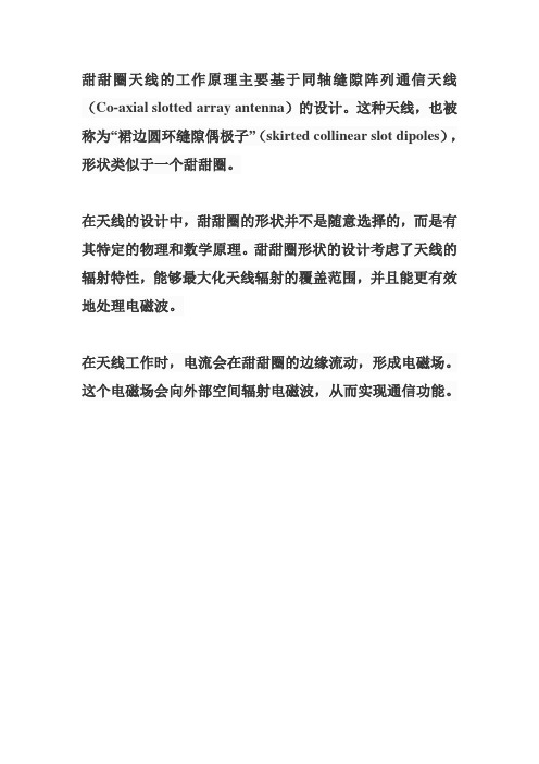
甜甜圈天线的工作原理主要基于同轴缝隙阵列通信天线(Co-axial slotted array antenna)的设计。
这种天线,也被称为“裙边圆环缝隙偶极子”(skirted collinear slot dipoles),形状类似于一个甜甜圈。
在天线的设计中,甜甜圈的形状并不是随意选择的,而是有其特定的物理和数学原理。
甜甜圈形状的设计考虑了天线的辐射特性,能够最大化天线辐射的覆盖范围,并且能更有效地处理电磁波。
在天线工作时,电流会在甜甜圈的边缘流动,形成电磁场。
这个电磁场会向外部空间辐射电磁波,从而实现通信功能。
一款新型宽频带缝隙微带天线设计

文章编号:员园园缘原员圆圆愿(圆园19)园3原园园18原03
吴电家菊等脑:交互与式电子信技术手息息册的技技术发术术展与应用研究 悦燥皂责怎贼藻则 葬灶凿 陨灶枣燥则皂葬贼蚤燥灶 栽藻糟澡灶燥造燥早赠
一款新型宽频带缝隙微带天线设计
程云鹏,单志勇
(东华大学,上海市,201620)
Design of Broadband Slit Microstrip Antenna
CHENG Yun-peng, SHAN Zhi-yong
(Donghua University, Shanghai 201620,China) Abstract:A novel ultra wide band patch antenna was conceived and designed, which consists of a circular radiation patch and an improved rectangular connecting floor. The small size of the antenna is achieved by using the open slot technology to increase current path, and the symmetric double T-shaped patch is loaded to form a gap radiation unit to increase the antenna bandwidth. Based on the simulation of the performance of the antenna by HFSS, the results show that the -10 dB impedance bandwidth of the antenna is 1.9-10GHz, and the maximum gain of the antenna is 10.1dB, which has good performance. It can be widely used in Bluetooth, WiMAX/WLAN systems, microwave communication systems and other working modes. Key words: microstrip antenna; broadband; gap slot; wireless communication
脊波导缝隙平面阵列天线的设计研究的开题报告
脊波导缝隙平面阵列天线的设计研究的开题报告一、课题背景及研究意义随着移动通信技术的飞速发展,人们对于通讯质量的要求也越来越高。
天线作为通信系统的重要组成部分,其性能的优劣直接影响着通信系统的质量。
面向更快、更稳定的通信服务,平面阵列天线逐渐成为业界关注的焦点。
目前,大多数平面阵列天线采用谐振耦合方式实现波束控制,但其波束宽度随着阵列元素的增多而减小,这对于实现大覆盖范围下的高速传输任务十分不利。
针对这一问题,研究人员提出了脊波导缝隙平面阵列天线。
该天线由脊波导缝隙微带天线和平面板导体组成,利用脊波导缝隙微带天线提供高增益、窄波束,平面板导体实现相邻基元之间的互耦和相位调节,可以实现波束宽度的控制,提高天线的性能。
本研究旨在设计一种脊波导缝隙平面阵列天线,并对其性能进行分析与优化,为天线应用进一步提升通信质量提供技术支撑。
二、研究内容1. 设计具有良好性能的脊波导缝隙平面阵列天线;2. 对阵列天线的特性进行仿真分析;3. 对天线的性能参数进行优化;4. 制作并测试脊波导缝隙平面阵列天线的性能,并与传统平面阵列天线进行比较分析;5. 对实验结果进行分析与讨论。
三、研究方法1. 利用HFSS软件建立阵列天线模型,进行电磁仿真;2. 对天线的增益、阻抗、选择性、波束宽度等性能指标进行分析与评估;3. 通过调整天线元素的参数以及阵列的布局来优化天线性能;4. 制作天线样机并进行性能测试,包括辐射特性、频率响应等;5. 对实验结果进行分析与讨论。
四、预期成果1. 设计出具有良好性能的脊波导缝隙平面阵列天线;2. 对阵列天线的性能参数进行优化;3. 制作出阵列天线的样机,并测试其性能;4. 为平面阵列天线在移动通信领域的发展提供新思路。
五、研究进度安排第一阶段:文献调研和理论分析,包括对脊波导缝隙微带天线、平面板导体的特性进行分析。
时间:两周。
第二阶段:建立脊波导缝隙平面阵列天线的仿真模型,对其性能进行仿真分析。
一种宽带圆形缝隙天线的设计

第6卷第6期空军工程大学学报(自然科学版)V o.l6N o.6 2005年12月J OURNAL OF AI R FORCE ENG I NEER I NG UN I VERSITY(NATURAL SC I ENCE ED I TI ON)D ec.2005 *一种宽带圆形缝隙天线的设计高向军,王光明,张晨新(空军工程大学导弹学院,陕西三原713800)摘要:在传统结构微带缝隙天线的基础上,设计了一种采用叉状馈电结构的宽带微带圆形缝隙天线。
通过调整馈电结构中主、侧臂的尺寸可以获得较好的匹配。
经过仿真和实验测试,该结构的宽缝天线工作于2GH z时,匹配带宽达到了32.5%(VS W R<1.5)。
关键词:微带;宽缝;叉状馈电;圆缝中图分类号:TN82文献标识码:A文章编号:1009-3516(2005)06-0028-03从微带天线的概念提出以来,对微带的理论研究一直是人们研究的热点,其工程应用非常广泛。
由于它剖面薄,重量轻,可与载体共形,易与有源器件集成等优点,已经被应用于卫星通信[1]、导航等领域。
今天,微带天线的形式已多种多样,微带缝隙天线以其独特的性能(馈电网络和辐射单元相对分离,从而把馈线对天线辐射方向图的影响降到最小)得到了广泛的应用。
微带缝隙天线具有对加工精度要求低,可用标准的光刻技术在敷铜电路板上进行生产等优点,尤其是微带宽缝天线更是有效地拓宽了频带[2,3]。
目前缝隙天线已被广泛地应用于航空航天飞行器、卫星直播电视等高频阵列天线中。
本文提出了一种采用叉状馈电结构的圆形宽缝天线,在改变馈点位置及叉状馈电结构中主、侧臂尺寸的情况下,可以获得良好匹配。
通过仿真及实验测试,这种结构的宽缝天线,工作于2GH z时,频带达到了32.5%(VS WR<1.5)。
1天线结构常见的圆形缝隙天线的结构如图1(a)所示。
它是在基片的地面开一圆缝,在基片的另一面利用508开路微带线馈电。
缝隙螺旋天线及其小型化设计
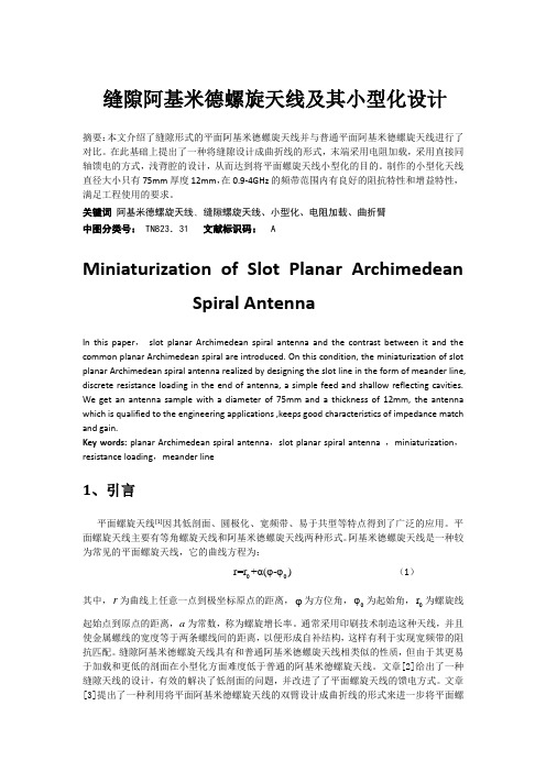
缝隙阿基米德螺旋天线及其小型化设计摘要:本文介绍了缝隙形式的平面阿基米德螺旋天线并与普通平面阿基米德螺旋天线进行了对比。
在此基础上提出了一种将缝隙设计成曲折线的形式,末端采用电阻加载,采用直接同轴馈电的方式,浅背腔的设计,从而达到将平面螺旋天线小型化的目的。
制作的小型化天线直径大小只有75mm厚度12mm,在0.9-4GHz的频带范围内有良好的阻抗特性和增益特性,满足工程使用的要求。
关键词阿基米德螺旋天线、缝隙螺旋天线、小型化、电阻加载、曲折臂中图分类号:TN823.31 文献标识码: AMiniaturization of Slot Planar ArchimedeanSpiral AntennaIn this paper,slot planar Archimedean spiral antenna and the contrast between it and the common planar Archimedean spiral are introduced. On this condition, the miniaturization of slot planar Archimedean spiral antenna realized by designing the slot line in the form of meander line, discrete resistance loading in the end of antenna, a simple feed and shallow reflecting cavities. We get an antenna sample with a diameter of 75mm and a thickness of 12mm, the antenna which is qualified to the engineering applications ,keeps good characteristics of impedance match and gain.Key words: planar Archimedean spiral antenna,slot planar spiral antenna ,miniaturization,resistance loading,meander line1、引言平面螺旋天线[1]因其低剖面、圆极化、宽频带、易于共型等特点得到了广泛的应用。
一种高增益缝隙定向天线设计

一种高增益缝隙定向天线设计张长慧;董胜;赵宪臣【摘要】In order to achieve a high-gain and low sidelobe antenna,a substrate integrated waveguide antenna array is designed. Choke Grooves are added between two neighboring radiation waveguides. Compared with traditional SIW slot antenna array, this improvement can greatly extend the operational bandwidth. SIW slot antenna array which meets both low side lobe and return loss requirement in desired bandwidth (8%)The experiments show that this antenna has good performance, and achieve the design requirement.%为实现高增益低旁瓣的定向天线,设计了一种采用介质基片集成波导实现缝隙天线阵,并在辐射缝隙两边增加扼流槽.与传统的介质基片集成波导相比,大幅增加了带宽。
最后实现了一介质基片集成波导天线阵,其带宽增加了8%。
实际测试表明该天线具有高增益,低旁瓣,达到了设计要求。
【期刊名称】《电子设计工程》【年(卷),期】2012(020)013【总页数】3页(P158-160)【关键词】介质基片集成波导;定向天线;扼流槽;波导缝隙【作者】张长慧;董胜;赵宪臣【作者单位】山东泉清通信有限公司,山东济南250100;山东泉清通信有限公司,山东济南250100;山东泉清通信有限公司,山东济南250100【正文语种】中文【中图分类】TN82介质基片集成波导实现缝隙天线阵是针对以往采用波导型材实现天线开缝的方法所提出的[1-3]。
- 1、下载文档前请自行甄别文档内容的完整性,平台不提供额外的编辑、内容补充、找答案等附加服务。
- 2、"仅部分预览"的文档,不可在线预览部分如存在完整性等问题,可反馈申请退款(可完整预览的文档不适用该条件!)。
- 3、如文档侵犯您的权益,请联系客服反馈,我们会尽快为您处理(人工客服工作时间:9:00-18:30)。
2
Singapore
3
Facts about Singapore
n n n n
A city country of 5.3 million residents (3.1 million local Singaporeans, 74.2% are Chinese) Land area of 704 km2 GDP per capita: $511 in 1965 to $54,775 in 2013 Key economy revenue: oil refinery, manufacturing, trade, and services
Microstrip-fed patch antenna
Radiation mechanism
16
Our Interest
n
Microstrip-Fed Slot Antennas
Ground-plane
Microstrip feed line
Substrate
17
Previous Studies
My Research Interests
n
Analysis and Design of Antennas
n
Frequency-Selective Structures and Absorbers
8
Outline
n n n
Brief Introduction to Slot Antennas Previous Studies on Microstrip-Fed Slot Antennas Our Recent Work
19
Microstrip-Fed Slot Antenna
ws 2.9mm
Ls 44.3mm
wm 4.8mm
r 2.2
h 1.6mm
Lm 12.8mm
20
Simulated Results
21
Microstrip-Fed T-Slot Antenna
T s lo t e tc h e d o n g ro u n d p la n e L s1 = 9 8 m m L s2 = 6 3 m m L d = 2 8 .5 m m W s= 6 m m W d= 3 m m W f= 4 .6 4 m m W s 11 11
n n
n
Experimental studies of narrow- and wideslot antennas Numerical techniques for analyzing the microstrip-fed slot antennas. Among the proposed methods, Green’s function in conjunction with the method of moments appears to be the most efficient. Extraction of equivalent circuits
11
The Founder of Slot Antenna
n
n
The most important technical advance in antennas after Hertz is the invention of the resonant slot as radiating element. In 1938, A. D. Blumlein (1903-1942) filed a patent for a slotted tube as antenna. Genius Engineer
22
Microstrip-Fed T-Slot Antenna (cont.)
0 -5
-10
-15
S11 (dB)
-20
measured data simulated data
– It retains all the advantages (lowprofile, light weight, ease of integration) that patch antennas have – wider bandwidth – smaller effect of a finite groundplane – smaller mutual coupling in the array configuration
r
2 . 45 , h 1 . 575 mm
M ic ro s trip fe e d lin e L s2 W
f
L s1 W
d
L f= 1 2 8 m m
Ld
[2] Z. Shen, C. T. Sze and C. L. Law, “A circularly polarized microstrip-fed T-slot antenna,” IEEE AP-S International Symposium Digest, pp. 1008-1010, 200n
n n
Definition: A slot antenna consists of a metal surface, usually a flat plate, with a hole or slot cut out. The metal surface can be a conducting plane, a waveguide wall, the ground plane of a microstrip line, etc. The slot cut can also take various forms: rectangular, circular, T-type, cross, etc. Slot antennas are extremely useful in many applications where low-profile or flush installations are required such as on high-speed aircrafts and missiles.
13
Simplest Slot Antenna
Dipole /4 /4 /4 Feed line /4 Metal sheet
Z1Z 2
0 2
4
35476
Babinet’s principle by Henry Booker
[1] H. G. Booker, “Slot aerials and their relation to complementary wire aerials (Babinet’s principle)”, J. I. E. E., 93, pp.620-626, 1946.
n
Suggestions for Future Work
9
The Pioneers
n n n
The very first wire antenna was due to Joseph Henry (1842). Heinrich Hertz invented both dipole and loop antennas (1887). Guglielmo Marconi received a signal across Atlantic ocean in 1901 .
14
Applications of Slot Antennas
Why Slot, Not Patch Antenna?
n
n
Microstrip patch antenna is basically a two-slot antenna array. Slot antenna is better because
The Theory Maxwell’s Equations
H
E
D
D J t B t
B 0
In 1864, James Clark Maxwell laid the theoretical foundation for electromagnetics.
6
School of EEE
n n
n
n n
One of the four founding schools There are 6 divisions (power, circuits and systems, information, control, communication and microelectronics) in the School. We have about 150 academic staff, 3500 undergraduate students, more than 1000 graduate students. Well equipped with world-class facilities .sg/eee 7
MICROSTRIP-FED SLOT ANTENNAS
Zhongxiang Shen
School of Electrical and Electronic Engineering Nanyang Technological University 50 Nanyang Avenue, Singapore 639798 Email: ezxshen@.sg
4
Nanyang Technological University
5
NTU’s Key Figures
n
n n n
Four colleges: Engineering, Science, Nanyang Business School, College of Humanities, Arts, and Social Sciences Undergraduate Students: 23,500 Graduate Students:10,000 Ranked 41st globally by QS World Rankings in 2013, with its Electrical Engineering Program ranked 31st worldwide. NTU is one of the fastestgrowing research universities in the world.