微带--波导转换Waveguide-to-Microstrip
W频段波导—微带的对脊鳍线过渡仿真设计
W频段波导—微带的对脊鳍线过渡仿真设计作者:金少华来源:《新生代·上半月》2018年第08期【摘要】:应用HFSS设计了一款W频(75.87-87.5)GHZ的对脊鳍线微带波导过渡结构,仿真结果表明,在W 频段(75.87-87.5)GHZ内,该过渡结构插损小于0.6dB,回波损耗在20dB以下,达到项目需要。
【关键词】:W波段波导微带过渡对脊鳍线1引言在毫米波接收系统中,各芯片间采用微带线连接.而毫米波测试系统用波导接口,需要低成本、低损耗的宽频带波导到微带过渡.常用过渡结构:阶梯脊波导过渡、对脊鳍线过渡、耦合探针过渡等.对脊鳍线过渡,因其可以采用印制版技术制作在价廉的软基片上,已成为一种普遍运用的过渡结构.本文通过软件HFSS设计并仿真了一个W波段的微带到波导鳍线过渡以满足工程项目的需要。
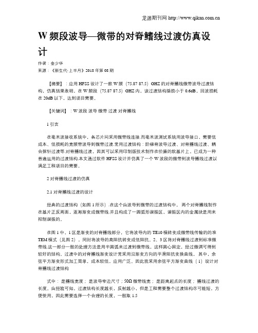
2 对脊鳍线过渡的仿真2.1 对脊鳍线过渡的设计经典的过渡结构(如图1所示).在这个由波导到微带的过渡结构中,两个对脊鳍线制作在基片正反两面,逐漸渐变成微带线.并且构成了一圆弧形谐振区,谐振区内的金属块是用来抑制谐振的。
在图1中,1区是渐变的对脊鳍线部分,它将波导内的TE10模转变成微带线传输的的准TEM模式(见图2),同时将波导的高阻抗转变成低阻抗。
2、3 区将对脊鳍线过渡到标准微带线.这一部分一般的处理方法是用半圆弧来过渡到微带线,这样圆心固定,经过微调可得到较好的结构。
过渡中的对脊鳍线渐变设计常采用沿渐变方向的平滑阻抗变换曲线,其中,余弦平方渐变形式加工简单,成本较低,应用广泛。
因此我采用余弦平方渐变曲线( 1)设计对脊鳍线过渡结构式中:是鳍线宽度;是波导窄边尺寸;50Ω 微带线宽;是距离起点的长度;鳍线过渡的长度。
由经验可知,过渡结构长度越长,反射越小,但是工程需要整个过渡结构尽可能短,方便使用,因此需要选择一个合理的长度,一般取1.5按照上述设计思路,我完成W波段(75.87-87.5)GHZ的过渡设计,介质基片采用RT-duroid 5880 材料(相对介电常数εr= 2 . 2),基片厚度为h = 0 .127mm ,金属条带厚度t=0.017 mm,标准矩形波导,宽a = 1.5494mm,高b =3.0988mm,50Ω微带线金属条带的宽度W = 0.358mm。
W波段波导—微带对脊鳍线过渡结构设计

Science &Technology Vision 科技视界0引言,。
,,。
:[1,2]、[3~4]。
,,,,。
,。
W 。
,80~95GHz 20dB,0.4dB。
1理论分析。
TE10,TEM 。
,,。
,WR10(2.54mm×1.27mm)。
50Ω[5]。
1。
,TE1090°,TEM [6]。
,,50Ω。
图1矩形波导—微带对脊鳍线过渡结构W 波段波导—微带对脊鳍线过渡结构设计单伟包超高志宇郑晓秦越(中国核动力研究设计院核反应堆系统设计技术重点实验室,四川成都610213)【摘要】文章基于对脊鳍线过渡结构设计并仿真了一种W 波段的矩形波导—微带线的转换器。
该转换器具有平面电路的几何结构优点,且空间体积小、质量轻,可广泛应用于毫米波平面传输线组成的电路中。
通过仿真结果表明:在W 波段(80~95GHz )的频带范围内,该过渡结构的回波损耗小于20dB ,插入损耗小于0.4dB 。
【关键词】W 波段;波导—微带转换;毫米波;对脊鳍线中图分类号:TN02文献标识码:ADOI :10.19694/ki.issn2095-2457.2021.12.45【Abstract 】This paper designs and simulates a W-band rectangular waveguide —microstrip line converter basedon the transition structure of the ridge—fin line.The converter has the advantages of planar circuit geometry structure,small space and light weight,and can be widely used in circuits composed of millimeter wave planartransmission lines.The simulation results show that:in the W band (80-95GHz)frequency band,the return loss ofthe transition structure is less than 20dB,and the insertion loss is less than 0.4dB.【Key words 】W band ;Waveguide to microstrip ;Millimeter wave ;Antipodal finline作者简介:单伟(1993—),男,汉族,硕士研究生,助理工程师,现主要从事核仪表系统技术研究。
基于LGA工艺的D波段微带线-波导过渡结构

第17卷第5期太赫兹科学与电子信息学报Vol.17,No.5 2019年10月Journal of Terahertz Science and Electronic Information Technology Oct.,2019文章编号:2095-4980(2019)05-0735-04基于LGA工艺的D波段微带线一波导过渡结构陈柏燊a,b,唐杨a,b,岳海昆a,b,朱华兵a,b,闻彰a,b,邓贤进a,b (中国工程物理研究院a.微系统与太赫兹研究中心,四川成都610200; b.电子工程研究所,四川绵阳621999)摘要:设计了一个工作于D波段的微带转波导结构。
过渡结构由2部分组成,分别为微带—带状线过渡结构和带状线一波导过渡结构。
相比传统的微带至波导结构,该结构无需额外的金属波导短路结构,减少了加工流程,直接和标准波导相连即可。
仿真结果表明,在122~140GHz范围内,反射系数小于-10dB,最小插入损耗为1.85dB。
该过渡结构基于栅格阵列(LGA)封装工艺,能够直接与其他的芯片和无源器件进行集成和封装,对射频微系统的集成具有重要意义。
关键词:过渡结构;微带线;带状线;波导;D波段,系统集成中图分类号:TN817文献标志码:A doi:10.11805/TKYDA201905.0735A D-band transition from microstrip to waveguide based on LGA technologyCHEN Boshen a-b,TANG Yang a,b,YUE Haikun",ZHU Huabing",WEN Zhang",DENG Xianjin"(a.Microsystem and Terahertz Research Center,China Academy of Engineering Physics,Chengdu Sichuan610200,China;b.Institute of Electronic Engineering,China Academy of Engineering Physics,Mianyang Sichuan621999,China)Abstract:A transition structure from microstrip to waveguide,based on Land Grid Array(LGA) package technology,is designed in this paper.The structure consists of microstrip to stripline transitionand stripline to waveguide transition.The metal waveguide shorter is no needed in the transition,thus themanufacturing process is simplified and the standard waveguide can connect with this transition directly.Simulation result shows that the minimal insertion loss is 1.85dB and the return loss is less than-10dBin122-140GHz.In addition,this transition can be integrated with other chips and passive devices.Therefore,the transition is useful for the improvement of property of RF microsystem.Keywords:transition;microstrip;stripline;waveguide;D-band;system integration微带线作为一种平面传输结构,容易与其他无源和有源微波器件集成,因此广泛用于微波单片集成电路和混合集成电路中。
波导带通滤波器与微带转换装置的设计
波导带通滤波器与微带转换装置的设计陈宪龙;罗勇【摘要】A K-band E-plane bandpass waveguide filter with seven-order inductance and a waveguide-tcrmicrostrip transition are designed using HFSS, a three-dimensional simulation software. The bandpass waveguide filter has 19 GHz center frequency, 3 GHz bandwidth, 0. 1 dB inband transmission loss, and less than-20 dB reflection coefficient. And the port reflection coefficient contributed by the waveguide-to-microstrip transition is less than-20 dB from 16 GHz to 20. 8 GHz bandwidth, and inband transmission loss is less than 0. 1 dB. Then the combination of the filter and the transition covers bandwidth from 17. 5 GHz to 20. 5 GHz in which in'uand transmission loss is less than 0. 3 dB, port reflection coefficient is less than-15 dB, out-of-band rejection is less than-30 dB, which meets the demands of the real system.%利用三维仿真软件HFSS首先设计了K波段7阶电感E面带通波导滤波器,以及波导-微带转换器.其中波导滤波器的中心频率为19 GHz,带宽为3 GHz,带内损耗小于0.1 dB,端口反射小于-20 dB;而波导-微带的转换器在16~20.8 GHz的带宽内端口反射小于-20 dB,带内损耗小于0.1 dB.然后将两者有效结合为一体,其工作带宽为17.5~20.5 GHz,带内损耗为0.3 dB,端口反射小于-15 dB,带外抑制小于-30 dB,可以满足实际系统应用的需求.【期刊名称】《现代电子技术》【年(卷),期】2012(035)021【总页数】3页(P68-70)【关键词】波导;带通滤波器;微带;波导-微带转换器【作者】陈宪龙;罗勇【作者单位】电子科技大学物理电子学院,四川成都 610054;电子科技大学物理电子学院,四川成都 610054【正文语种】中文【中图分类】TN814-340 引言随着毫米波技术在现代无线通信系统中的广泛应用,对各种高性能毫米波集成电路的需求也日益增长。
双脊波导和微带转换

双脊波导和微带转换
双脊波导和微带线(Microstrip Line)是微波和射频领域中用于传输电磁波的两种不同的传输线结构。
微带转换通常是指将信号从微带线传输到双脊波导或从双脊波导转换到微带线的过程。
双脊波导(Double Ridge Waveguide):
* 结构:双脊波导是一种中空的波导结构,具有两个脊(ridge),脊之间有中空区域,通常用于传输高频电磁波。
* 优点:双脊波导能够支持宽带传输,对于高频和毫米波应用具有一定的优势。
* 应用:在毫米波通信、雷达系统和天线设计等领域中常见。
微带线(Microstrip Line):
* 结构:微带线是一种在介质基板上的导电条带,通常在一面是导体,另一面是大地平面。
这种结构可以实现相对低成本、轻质、容易集成的设计。
* 优点:微带线结构适用于集成电路和板上系统设计,易于制造和集成。
* 应用:在微波和射频电路、天线、通信系统中广泛应用。
微带转换:
微带转换通常指的是设计用于在微带线和其他传输线(如双脊波导)之间进行信号转换的元件。
这些元件可以包括:
微带到波导过渡:设计用于将信号从微带线传输到波导的结构,以适应不同传输线的特性阻抗匹配。
波导到微带过渡:与上述相反,将信号从波导传输到微带线的结构,同样需要阻抗匹配。
微带到双脊波导过渡:用于将信号从微带线传输到双脊波导的设计。
这些过渡元件的设计需要考虑阻抗匹配、传输特性、频率响应等因素,以确保信号的有效传输和最小损耗。
在微波和射频系统中,过渡元件的设计是一项复杂而关键的工程任务。
H面波导到微带过渡结构设计

舰 船 电 子 工 程
S h i p El e cg
Vo 1 . 3 3 No . 1 2
1 5 5
2 0 1 3年 第 1 2 期
H 面 波 导 到 微 带 过 渡 结 构 设 计
兰 云鹏 吴景峰 王 抗 旱
LAN Yun p e n g W U J i n g f e ng W ANG Ka ng ha n
( He b e i S e mi c o n d u c t o r R e s e a r c h I n s t i t u t i o n ,S h i j i a z h u a n g 0 5 0 0 5 1 )
插损过渡成为重点关注 的问题。
波导一 微带过渡结 构 多样 , 常见 的过 渡结 构有 : 耦 合探 针过渡口 ] 、 脊 波导过渡_ 4 ] 、 对 脊鳍 线过渡[ 5 ] 等 。其 中耦合探 针过渡分为 : 电场耦合 和磁 场耦合 。电场 耦合 采用 的是 在 波导宽边插入 E面探针的结构方式_ 6 ] 。磁场耦 合过渡 目 前国 内少见报道 , 电子科技大学徐军教 授等人在 2 0 1 0年 提 出了一种磁耦合 的波导一 微带 转换结构 l 8 ] , 该结 构先 利用偏 心同轴线将微带 中传播 的准 T E M 模 转化为 T E M模 , 然后 通过末端接地 的半 圆环金属 条带在 波导 中激起 T E o 模, 完
Abs t r a c t Th e p a p e r d i s c u s s e d a n H— p l a n e wa v e gu i d e - mi c r o s t r i p t r a n s i t i o n . Th e p r o b e wa s pa r a l l e l t o H— p l a n e a n d i n s e r t e d t o t h e wa ve g u i d e f r o m t h e s h or t s i d e o f t h e wa v e g u i d e . HFSS wa s u s e d t O s i mu l a t e a n d o p t i mi z e t h e l o c a t i o n a n d wi d t h o f t h e p r o b e .A b a c k t o ba c k t r a ns i t i o n wa s f a b r i c a t e d a n d me a s u r e d.t h e r e s ul t s h o we d U S t h a t t h e i ns e r t i o n 1 O S S be t we e n 3 0 GH z ~3 6 GHz wa s 1 e s s t h a n 0 . 8d B,a nd t h e r e t ur n l o s s wa s g r e a t e r t ha n 1 6 d B The s t r u c t u r e h a d t h e a d v a nt a g e s o f s i mp l e s t r u c t u r e ,l o w i n s e r t i o n l o s s,wi d e b a nd ,e a s y f a b r i c a t i o n e t c . Ke y W or d s H— Pl a ne ,ma g ne t i c c o u pl i n g,Ka b a n d,wa v e g ui de - mi c r o s t r i p ,t r a n s i t i o n Cl a s s Nu ml  ̄r TN7 1 3
微带-波导转换教材
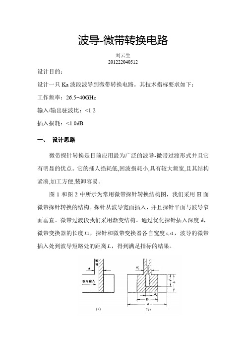
波导-微带转换电路刘云生201222040512设计目的:设计一只Ka波段波导到微带转换电路。
其技术指标要求如下:工作频率:26.5~40GHz输入/输出驻波比:<1.2插入损耗:<1.0dB一、设计思路微带探针转换是目前应用最为广泛的波导-微带过渡形式并且它有明显的优点。
它的插人损耗低,回波损耗小,具有较大频宽,且其结构紧凑,加工方便,装卸容易。
图1和图2中所示为常用微带探针转换结构图,我们采用H面微带探针转换的结构。
探针从波导宽面插入,并且探针平面与波导窄面垂直。
微带过渡段我们采用渐变结构。
通过优化探针插入深度d,微带变换器的长度1L,探针和微带变换器各自宽度,1s s,波导的微带插入处到波导短路处的距离L,得到满足指标的结果。
图1 H面微带探针转换结构图图2 E面微带探针转换结构图二、设计过程:(1)利用ADS软件里的微带计算工具得出中心频率为33.5GHz处的微带的宽度0.77,如图3所示。
Sx mm图3 50欧姆微带线宽(2)在HFSS中建立仿真模型如图4所示,包括微带金属条,微带基板,以及包围空气腔三部分。
利用对称性以YZ面为对称面切掉一半可以减少计算时间。
图4 仿真模型(3)设置三部分的材料属性,其中微带金属条为PEC,微带基板为Duriod5880(厚度0.254mm=)。
包围空气=,相对介电常数 2.2腔设为真空(默认)。
(4)设置波端口1,2。
都为1个模式,如图5。
图5 波端口1 波端口2(5)设置边界条件如图6。
其中微带被包围空气腔的上面设置辐射边界,对称YZ面设置为Prefect H面。
图6 边界条件(6)设置求解,扫频。
然后设置5个优化变量(优化探针插入深度以及微带变换器的长度,1s s,波导的微带插入处到波d L,宽度,1导短路处的距离L),优化目标即为设计指标。
三、设计结果及存在问题分析:通过优化得到最佳优化值如下图7中所示:图7 优化变量优化结果为:图8 优化结果图驻波比在整个频段内均小于1.2,插入损耗在整个频段内均小于0.3dB,故在全频段内满足设计要求。
毫米波宽带H面波导微带转换结构
毫米波宽带H面波导微带转换结构李钰;翁鹏飞【摘要】微带探针的波导微带的转换结构基于直接插入波导的微带探针激励方法设计,是一种用于毫米波单片微波集成电路(MMIC)芯片封装测试的波导-微带转换结构。
运用微带探针直接插入波导进行场的激励方式,可使得整体结构更加简单、紧凑,并且具有无需焊接和安装方便等优点。
利用三维电磁仿真软件(HFSS)对Ka波段波导的H面探针方式波导-微带转换装置进行了仿真与优化设计,结果表明在26.5-40 GHz的波导全带宽内,端口的反射系数小于-20 dB,带内损耗小于0.3 dB。
%The probe conversion structure of waveguide to microstrip is based on the microstip probe excitation method into the waveguide in the designation. And it is used in the monolithic microwave integrated circuit (MMIC) for the measure of the chip and packaging. Based on the microstrip probe into waveguide to conduct the field mode excitation, it can be more simple, compact and easy installation. Using the three-dimensional electromagnetic simulation software (HFSS) in the Ka band for the simulation and optimization of the waveguide to microstrip structure, the results shows the reflection coefficient of port is less than-20dB, the insertion loss is less than 0.3dB in the 26.5-40 GHz band.【期刊名称】《电子设计工程》【年(卷),期】2015(000)024【总页数】3页(P90-92)【关键词】波导微带转换;宽带;微带探针;H面【作者】李钰;翁鹏飞【作者单位】华东师范大学上海 200062;华东师范大学上海 200062【正文语种】中文【中图分类】TN302随着毫米波技术在现代无线通讯系统中的广泛应用,对各种高性能单片微波集成电路(MMIC)的需求也日益迫切。
微带-波导过渡结构及其应用

微带-波导过渡结构及其应用摘要:本文介绍了一种微带与波导过渡结构,该结构通过金属柱将微带线与波导顶部连接,将微带线的地与波导底部连接,同时引入合适的金属块调节,使得微带信号较好地在指定频段过渡到波导结构。
应用该结构,本文设计了一个滤波主体结构为腔体结构、输入输出为微带线结构的滤波器,使得该滤波器在具备低损耗的同时又便于与平面微带电路集成。
仿真结果显示该滤波器性能优良,验证了设计的有效性。
1 引言现代通信系统对高性能滤波器的要求和需求都非常高。
滤波器不仅需要具备更小的尺寸,更低的插入损耗,还需要更好的选择性能[1-10]。
基于微带或带状线等结构的滤波器一般尺寸较好,且易于其他平面电路结合,但是由于介质板损耗、辐射损耗和金属损耗,这些滤波器通常带内损耗都较大,实际应用具有较大局限性。
波导类滤波器由于没有辐射损耗,介质损耗也基本可不予考虑,主要存在的是金属损耗,其谐振器的品质因数一般远高于微带、带状线等结构的谐振器,构成的滤波器一般带内损耗要远小于平面结构的滤波器。
但一般腔体滤波器与平面电路较难集成,其间通过线缆连接往往又会占据较大的面积。
为了既能利用波导滤波器损耗低的优点,又能便于与平面电路集成,本文给出了一种微带线与波导的过渡结构,使得信号通过该结构能顺利地由微带线传输到波导中。
在此基础上,本文给出了一个应用该结构的滤波器实例,在兼顾集成的同时又可使得整个滤波器具有较低的插入损耗。
2 微带线-波导过渡结构图1给出微带线-波导过渡结构的示意图,其中波导结构的底部是由介质板顶部的金属地构成的,金属过孔将介质板底部的地与介质板顶部的金属地相连接;微带线通过波导壁上的开孔进入波导腔,与金属地之间以间隙隔开,微带线的末端通过金属柱与波导顶部连接,同时在波导顶部引入适当的金属块以调节两种传输模式之间的良好匹配。
图1 微带线-波导过渡结构示意图 a. 外观 b. 去除波导壁后的视图3 滤波器设计在上述微带线-波导过渡结构基础上,本文设计了一个包含该过渡结构的滤波器,如图2所示。
A TRANSITION FROM MICROSTRIP TO WAVEGUIDE

专名称:A TRANSITION FROM MICROSTRIP TO WAVEGUIDE
发明人:BUCK, Christopher, M. 申请号:IB2002001010 申请日:20020327 公开号:WO02/082579P1 公开日:20021017
摘要:A transition from microstrip to waveguide comprises a rectangular waveguide and a microstrip structure formed by a resilient substrate (24) having a stripline (26) on one surface and a ground plane (44) on an opposite surface, the conductors (26, 44) being interconnected by viaholes. The substrate (24) is disposed between the side walls (36) and the floor (22) of the waveguide with the ground plane contacting the floor. The stripline extends from one end of the waveguide along a portion of its length. A tapered ridge (38) depends from the ceiling (34) of the waveguide and extends from the other end of the waveguide. A terminal end (40) of the ridge contacts a terminal portion of the stripline under mechanical pressure. The ridge (38) may have a choice of profiles such as triangular, half cosine and half cosine with a semicircular cut-out in the upright edge.
波导微带

罴 疆 鬟
200"8·15 10:36.11
频率(GHz)
图4仿真结果
7
3结论 基于场模式匹配以及阻抗变换的方法在不同传输系统转换设计中常常使用,此过渡解
决了脊波导重复安装导致性能下降的问题,可望在实际中验证和使用。
参考文献 【I】薛良金<毫米波工程基础)哈尔滨工业大学出版社2004年 【2】 JiaLin Li, Wei Shao ”A NOVEL WAVEGUIDE-TO-MICROSTRIP TRANSITION FOR
A-A。截面电场分布
B-B’截面电场分布
C-C’截面电场分布D-D’截面电场分布 图2各截面所对应的电场分布图
在csr中背对背仿真的结构如图3所示
图3背对背的过渡结构 通过宽带阶梯加脊波导把矩形波导的主模波阻抗变换到微带特性阻抗以实现过渡·在 这种结构中,加脊波导由一些减高波导组成,以便使波导高度从b逐渐变化到低阻抗实现 阻抗匹配,通过查表我们可以得到3阶切比雪夫阻抗变换器的数值,从而确定该过渡的物 理尺寸.脊波导特性阻抗可以采用近似公式…计算。波导采用BJ320(a-7.12mm,b23·56mm), 介质的相对介电常数为2.2,厚度为0.254m:阶梯的高度相差0.5u.长度分别为:i.6mm, 1.4mm,2.0mm,介质探入波导的长度为2.3mm。仿真结果如图4,我们可以看到在 3lGffz一40GHz其回波损耗均在lOdB以下,插损在0.6dB左右。
意如图1所示:
A
BC D
A‘
B。C‘D‘
圈1过渡的纵剖国
那么各个截面上的电场分布如图2所示,在A—A’截面上传播的是波导的主模T卧,经 过脊波导的变换。场逐渐被集中压缩到介质之中,场模式也从TE-n逐渐变化到微带线上的 TEM波模式,从而实现了波导到微带的变化,脊波导不仅实现了场模式的匹配,而且也完 成了阻抗匹配…。
W波段波导_微带探针过渡设计

W波段波导-微带探针过渡设计付骥 胡皓全( 电子科技大学电子工程学院,成都 610054 )摘 要:本文采用高频仿真软件HFSS仿真设计出了W波段E面探针方式的波导到微带过渡结构,并制作了实物进行了测试,实测结果表明在频率85GHz-100GHz范围内,过渡的插入损耗小于1dB,与仿真结果基本吻合,适合工程应用。
关键词:毫米波;W波段;波导微带变换Design of W Band Waveguide to Microstrip Probe TransitionFU Ji, HU Hao-quan(School of Electronic Engineering, University of Electronic Science and Technology of China, Chengdu 610054, China) Abstract: In this paper, a structure of W band waveguide to microstrip probe transition is designed and analyzed by using the advanced electromagnetic simulation software HFSS. The transition is also fabricated and measured to demonstrate the performance, the measured results show that the insertion loss of the transition is less than 1dB in the frequency of 85GHz to 100GHz, which shows good agreement with theoretical results.Key words:Millimeter wave; W band; Microstrip probe transition引 言随着毫米波技术的发展,毫米波混合集成电路与单片集成电路在通信、雷达、制导以及其它一些系统中得到广泛应用,微带传输线正在越来越多的场合取代金属波导,成为制作毫米波集成电路的重要传输线。
Ka频段波导—同轴探针—微带过渡的研究

Ka 频段波导—同轴探针—微带过渡的研究刁睿,徐锐敏,谢小强电子科技大学电子工程学院,四川成都 (610054)E-mail :screamtodie@摘 要:本文介绍了一种设计波导—同轴探针—微带过渡结构的方法。
设计采用HFSS 分析并进行优化,在26.5-39GHz 范围内,插入损耗小于0.11dB ,输入端回波损耗小于-19.5dB ,最小可达-24dB 。
关键词:毫米波,同轴探针,过渡中图分类号:TN631. 引 言在毫米波频段,为便于测试、天馈以及独立微带电路之间的连接,常常需要将微带电路输入、输出端口通过转换结构过渡到矩形波导。
在需要将信号作一段距离的传输时,也必须将电路从微带转换至波导,以降低传输损耗。
因而采用微带的毫米波集成电路往往都必须具有宽带特性的波导-微带过渡的接口。
探针结构是工作于TEM 模的同轴线和工作于10TE 模的矩形波导间的一种常用的过渡结构[1]。
在实际应用中,过渡器的一个不可忽视的附加因素是气密要求。
很多微带电路,特别是军用微带电路,为保证能在各种恶劣环境条件下性能的稳定性,对系统的气密性提出了更高的要求。
而通常所采用的E 面探针型波导—微带过渡结构在波导上的开口较大,不仅使系统的气密性受到一定的影响,对矩形波导内的场分布也将产生较大的扰动。
综合运用相关理论知识并考虑到波导—微带过渡结构的具体要求,采用波导—同轴探针—微带过渡结构将能够获得较好的效果。
为此本文对波导—同轴探针—微带过渡结构的设计方法进行了介绍。
2. 理论分析探针在波导中相当于一个小天线,若同轴线接波源,探针便是发射小天线,它向波导所限定的辐射电磁波. 一般地说,只要电磁波的电场或与波导某模式的电场或磁场分量一致,该模便会被激励。
本文讨论单探针激励矩形波导[2],如图1所示。
采用R.F.Harrington 的等效电路法来进行研究。
在矩形波导内,由同轴波导驱动一根很细的探针,如图所示,细探针被放置在z=0的波导模截面上。
ADS2009 常用元器件介绍
ADS2009 常用元器件介绍录入: 点击:37151.集总参数元件组成电路模型的元件都是能反映实际电路中元件主要物理特征的理想元件。
电路中元件在工作过程中还与电磁现象有关,常见的3种最基本的理想电路元件有:表示消耗电能的理想电阻元件R;表示储存电场能的理想电容元件C;表示储存磁场能的理想电感元件L。
当实际电路的尺寸远小于电路工作时电磁波的波长时,可以把元件的作用集总在一起,用一个或有限个R、L、C元件来描述,这样的电路称为集总参数电路。
集总参数元件是具有两个端钮的元件,从一个端钮流入的电流等于从另一个端钮流出的电流,端点间的电压为单值量。
在原理图设计窗口中的“Lumped-Components”主件控制面板可以选择集总参数元件,其中主要包括电感、电容和电阻等常用集总参数元件。
1)电容(1)一般电容:一般电容符号如图2-19所示,其主要参数见表2-2。
表2-2 一般电容参数(2)含Q值电容(CAPQ):Q值是衡量电容的重要指标,含有Q值电容电路符号如图2-20所示,其主要参数见表2-3。
表2-3 含有Q值的电容参数(3)直流阻塞电容(DC_Block):直流阻塞电容是用于在电路中隔掉直流成分的理想器件模型,其电路符号如图2-21所示,其主要参数见表2-4。
直流阻塞电容对暂态分析是非因果的,参数C和L通常用于暂态分析,且电容的值是有限值(默认为1μF)。
2)电感(1)一般电感:一般电感符号如图2-22所示,其主要参数见表2-5。
表2-5 一般电感参数(2)含Q值电感(INDQ):Q值是衡量电感的重要指标,含有Q值的电感符号如图2-23所示,其主要参数见表2-6。
(3)交流阻塞电感(DC_Feed):交流阻塞电感是用于在电路中隔掉交流成分的理想器件模型,其电路符号如图2-24所示。
其参数与直流阻塞电容一致。
3)电阻一般电阻符号如图2-25所示,其主要参数见表2-7。
4)RLC连接结构除了单个的集总参数元件外,ADS还提供了集总参数元件的各种连接方式,主要有电感电容并联结构和电感电容串联结构。
Ku频段波导微带转换的设计与分析

Ku频段波导微带转换的设计与分析陈小忠;闫书保【摘要】Designs and processes a waveguide-microstrip converter applied in Ku band by using HFSS software. The waveguide-microstrip converter adopts the probe plane and narrow waveguide wall vertical structure. Simulation of return loss small than -30dB, insert loss less than 0.3dB, actual test return loss is less than-18dB, single loss is 0.3dB.%利用HFSS仿真软件,设计并加工一个用于Ku频段的波导微带转换器.该波导微带转换采用探针平面与波导窄壁垂直的结构. 两端口仿真回波小于-30dB,差损小于0.3dB,实际测试回波小于-18dB,单个波导微带转换端口差损为0.3dB.【期刊名称】《现代计算机(专业版)》【年(卷),期】2015(000)018【总页数】4页(P58-61)【关键词】HFSS仿真;波导微带转换;Ku频段【作者】陈小忠;闫书保【作者单位】广州海格通信集团股份有限公司,广州 510663;广州海格通信集团股份有限公司,广州 510663【正文语种】中文随着微波技术的发展,往往要求能量在不同的介质中进行传输。
而且微带线正逐步取代金属波导,成为微波电路小型化的重要部分。
就目前而言,波导微带过渡主要有脊波导、过渡鳍线、微带探针等几种形式。
脊波导与微带的连接通常采用硬压力接触,这就导致其性能与压力接触相关,所以其可靠性较差。
鳍线存在较多的电磁波模式,而且对其进行抑制较为困难,另外,鳍线在截至频率时会产生一个纯电抗特性的源阻抗或负载阻抗,使有源器件处于不稳定区域,容易出现自激。
V波段微带波导过渡设计
第2期2019年2月Vol.14No.2Feb.2019 Journal of CAEIT程与应用doi:10.3969/j.issn.1673-5692.2019.02.016 V波段微带-波导过渡设计张运传,刘志红(华东电子工程研究所,安徽合肥230031)摘要:本文介绍了一种应用于汽车防撞雷达收发前端测量的V波段微带-波导过渡设计。
利用高频仿真软件HFSS对过渡结构进行了仿真优化并进行了实物制作。
对过渡进行了测试并和仿真结果进行了对比分析。
结果表明该过渡可以满足实际测试需求。
关键词:V波段;微带-波导过渡;防撞雷达;仿真优化中图分类号:TN402文献标识码:A文章编号:1673-5692(2019)02-0203-03Design of V-Band Microstrip-Waveguide TransitionZHANG Yun-chuan,LIU Zhi-hong(East China Research Insititute of Electronic Engineering,Hefei230031)Abstract:This paper introduces a V-l)and microstrip-waveguide transition design applied to the front end measurement of vehicle collision-avoidance radar.The high frequency simulation software HFSS is used to simulate and optimize the transition structure.Then it is realized.Both simulation and measurement are compared and analyzed.The results show that the transition can meet the actual testing requirements.Key words:V-band;microstrip-waveguide transition;collision-avoidance radar;simulation and optimi・zationo引言随着毫米波技术的日益发展,单片微波集成电路(MMIC)的使用越来越广泛。
- 1、下载文档前请自行甄别文档内容的完整性,平台不提供额外的编辑、内容补充、找答案等附加服务。
- 2、"仅部分预览"的文档,不可在线预览部分如存在完整性等问题,可反馈申请退款(可完整预览的文档不适用该条件!)。
- 3、如文档侵犯您的权益,请联系客服反馈,我们会尽快为您处理(人工客服工作时间:9:00-18:30)。
Narrow Band Ridge Waveguide-to-Microstrip Transition for Low Noise Amplifier at Ku-BandZahid Yaqoob Malik, Abdul Mueed, Muhammad Imran NawazCentre for Wireless CommunicationNational Engineering and Scientific CommisionAbstract- A compact Ku-band waveguide-to-microstrip transition integrated with low noise amplifier is designed. It acts as an interconnect between waveguide antenna and RF receiver modules. The transition design consists of standard waveguide WR62, a cavity for the low noise amplifier and a solid transformer section in the form of a staircase called ridge. The ridge is fixed in the bottom wall of a waveguide with the help of a screw. The centre conductor of a coaxial connector is brought near this transformer but doesn’t touch the transformer; these elements together with the back of the staircase and an adjacent portion of the bottom wall define a magnetic field coupling loop. This design methodology gives us narrow bandwidth of 500MHz at Ku-band and hence eliminates the need for a filter in receiver section for specific applications.I.I NTRODUCTIONLower loss of waveguide at higher frequencies above X band is advantageous as compared to the coaxial line. At higher frequencies, waveguide-to-microstrip transitions replace waveguide to coaxial transitions to act as interconnects between modules and antennas. These transitions can be also be made to operate at Millimeter wave bands. Waveguide is made from a single conductor which usually propagates a dominant TE mode, having a cutoff frequency below which the waveguide is highly attenuative.Most of the transitions are designed to operate within the frequency band of dominant mode propagation only. As compared with coaxial line, waveguide modes have impedance characteristics that tend to make transition design more challenging. The impedance of each of waveguide modes changes with frequency. In addition, the impedances of standard waveguides are much greater than 50 ohms, typically a few hundred ohms. Consequently, the bandwidth for most waveguide-to- microstrip transitions rarely reaches the full dominant mode bandwidth [1].Microstrip-to-waveguide transitions have been widely used in testing and evaluating millimeter-wave hybrid and monolithic integrated circuits and combining integrated circuits with waveguide components [2]. The present transition relates to a ridge waveguide-to-microstrip line transition for an amplifier which uses a field effect transistor (FET) or the like. Generally, a waveguide-to-coaxial line transition or a waveguide-to-microstrip line transition is employed to supply an FET with a microwave signal coming in through antenna [5]. The transition apparatus may off-course utilize the magnetic field associated with the electromagnetic wave energy propagating in the waveguide. If the inner conductor of the coaxial transmission line is utilized as a probe to couple to this magnetic field, then the longitudinal axis of the coaxial line may be aligned with the propagating axis of the waveguide. With such an orientation of axes, the overall structure requires less space than those depending upon electric field coupling [6].This transition provides a simplified and compact structure for waveguide-to-coaxial transmission line. This transition consists of three main subassemblies. The first part is a standard Ku-band waveguide WR62. The second part is impedance transforming section which is mounted in the WR62 waveguide with the help of a screw, the third part is the low noise amplifier cavity having the centre pin of coaxial transmission line. This pin is brought close to the staircase transformer to a side with the waveguide on one end and other end is connected to the alumina substrate used for the low noise amplifier in the cavity. Rest of the paper is organized as follows. The design of the ridge is discussed in section II. Section III discusses simulation work. In section IV, manufacturing details and test results are presented. The work is concluded in section V.II.D ESIGN OF THE R IDGEImpedance Matching Section is designed to match the higher impedance of a waveguide section to a coaxial line, the general practice is to decrease the narrow dimension of the waveguide, that is, the distance between the broadwalls of a rectangular waveguide in a series of steps so as to arrive at an internal dimension that achieves an acceptable impedance match with a satisfactory voltage standing wave ratio (VSWR). The impedance matching transformer (ridge) consists of five quarter wave sections as shown in figure 1. These sections take the form of a staircase of individual steps. The heights of the steps which are generally unequal are chosen in accordance with a set of numerical coefficients referred to as Techbyscheff coefficients [3]. The distance AB between the cavity wall and the end face of the first step is between 0.01λ and 0.1 λLNA cavity is approximately one quarter of a wavelength. The width of each step is generally between one third and onethe first transformer section. This impedance level is dependentFig.1. Ridge Designupon the impedance of the particular coaxial line (50 ohm in this case) and the particular waveguide (WR62 in our case). We have finally adjusted all the above mentioned critical distances using HFSS software.III.S IMULATION OF T RANSITIONWe have simulated the above said transition in the HFSS and after some optimization the transition met the designed specifications, at this stage we freeze the dimensions and generated a physical model. The HFSS model of the transition is shown in figure2 and the final dimensions of the transformer are depicted in figure 3.The results of the simulation are given below:Fig.2. HFSS ModelFig.3. Ridge DesignFig.4. Input Return LossFig.5. Output Return LossFig.6. Insertion loss of the TransitionThe figure 7 shows the model of the complete ridge waveguide-to-microstrip transition with LNA cavity. The details of the LNA design are beyond the scope of this paper and hence will not be discussed.Fig.7. CAD Model of the Ridge Waveguide-to-Microstrip Line Transition with Low Noise amplifier cavityIV. M ANUFACTURING & T EST R ESULTSThe above mentioned Ridge Waveguide-to-Microstrip Line Transition with Low Noise amplifier cavity is manufactured in parts and finally integrated using silver conductive epoxy (aluminum or laser welding can also be used). The pin is connected to the Alumina with 1 mil gold bonding wire in order to connect it with amplifier circuit in the LNA cavity. The pictures of individual three parts and integrated assembly is presented below:Fig.8. Integrated AssemblyFig.9. Ridge TransformerFig.10. Waveguide FlangeFig.11. WaveguideThe manufactured transition Ridge Waveguide-to-Microstrip Line Transition with Low Noise amplifier cavity was tested in two steps. In the first step LNA cavity was filled with transmission line and VSWR and Insertion loss was measured using Vector Network Analyzer. The values of dimensions CD, AB and HT are adjusted real-time for best results. The measured results are given below:Fig.12.Input Return LossFig.13.Output Return LossFig.14.Insertion LossThe input and output return losses are found to be 10dB and 14dB respectively in desired 500MHz bandwidth. Also the insertion loss is found to be 2.2dB. Then low noise amplifier was built inside the cavity and measured with the help of vector network analyzer and noise figure meter the results were satisfactory and are presented below:Fig.15.Input Return Loss Fig.16.Output Return LossFig.17. Gain S21Fig.18. Isolation S12TABLE IP ERFORMANE OF LNA WITH W AVEGUIDE-TO-M ICROSTRIPT RANSITIONV.C ONCLUSIONSA Narrow Band Ridge Waveguide-to-Microstrip Line Transition for Low Noise Amplifier at Ku Band is designedand manufactured. The structure is very compact, and it createsa hermetic seal without any additional piece in a waveguide.The transition is compatible with MMIC technology, because itcan be integrated easily in the bottom of MMIC housing. The transition is ideally suited for future mm-wave applications using alumina for MMIC substrate and circuitry housing. It canbe used without an additional filter needed in front of LNA inthe receivers.A CKNOWLEDGEMENTSWe would like to thank Mr. Zahir Hussain Babar for his technical support. We would also like to thank Mr. Hassan Mansoor of Mechanical Design Realm for manufacturing facilities and suggestions.R EFERENCES[1] Eric Holzman, “Essentials of RF and MicrowaveGrouding” Artech House Boston/London.[2] Hui-wen Yao, Amr Abdelmonem, Ji-Fuh Liang andKawthar A. Zaki, “A Full Wave Analysis of Microstrip-To- Waveguide Transitions”, 1994 IEEE MTT-S Digest. [3] Hui-wen Yao, Amr Abdelmonem, Ji-Fuh Liang andKawthar A. Zaki, “Analysis and Design of Microstrip-To- Waveguide Transitions”, IEEE TRANSACTIONSON MICROWAVE THEORY AND TECHNIQUES,VOL.42,NO.12,DECEMBER 1994.[4] Paul Wade, “Rectangular Waveguide to Coax TransitionDesign”.[5] EUROPEAN Patent Application, Publication number0074613.[6] United States patent, Patent Number 3737812.。