基于LM2596-ADJ-DCDC稳压器的高效率恒流稳压电源设计最新版本
lm2596的资料

V V(min) V(max) % 2
η
效率
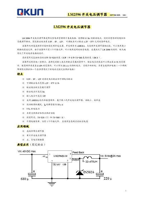
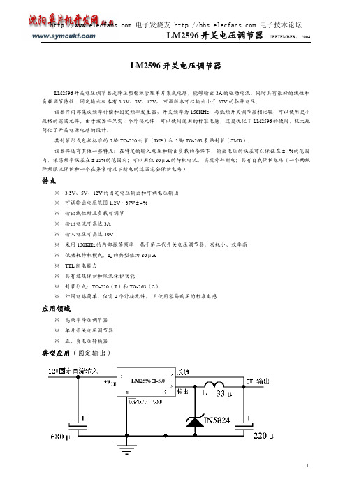
LM2596 开关电压调节器
符号 LM2596□—12 参量 (见注 14) 15V≤VIN≤40V, 0.2A≤ILOAD≤3A VIN=25V,ILOAD=3A 88 12.0 11.52/11.40 12.48/12.60 条件
SEPTEMBER, 2004
D1----5A/40V IN5825
图 1 标准测试电路
在开关调节器中,PCB 版面布局图非常重要,开关电流与环线电感密切相关,由这种环线电感所产生的暂态电 压往往会引起许多问题。要使这种感应最小、地线形成回路,图中所示的粗线部分在 PCB 板上要印制得宽一点,且 要尽可能地短。为了取得最好的效果,外接元器件要尽可能地靠近开关型集成电路,最好用地线屏蔽或单点接地。 最好使用磁屏蔽结构的电感器,如果所用电感是磁芯开放式的,那么,对它的位置必须格外小心。如果电感通量和 敏感的反馈线相交叉,则集成电路的地线及输出端的电容 COUT 的连线可能会引起一些问题。在输出可调的方案 中,必须特别注意反馈电阻及其相关导线的位置。在物理上,一方面电阻要靠近 IC,另一方面相关的连线要远离电 感,如果所用电感是磁芯开放式的,那么,这一点就显得更加重要。 5
4
LM2596 开关电压调节器
测试电路及其布线方案(固定输出)
SEPTEMBER, 2004
注:反馈线要远离电感,电路中的粗线一定要短,最好用 地线屏蔽。 纹波滤波电路 CIN---470μF/50V COUT----220μF/25V L1---68μH,L38 D1----5A/40V IN5825
说明:标准字体对应的项目适合于 TJ=25℃时,带下划线的粗斜体字对应的项目适合于整个温度范围; 系统参量(4) 测试电路见图 1
基于-LM2596的DC~DC电路分析

基于-LM2596的DC~DC电路分析电路总体说明LM2596属于DC-DC 开关电源的BUCK 类电压反馈式的降压型电源管理集成电路,能够输出5V/3A 的驱动电流,开关频率150KHz 。
在本电路(图1)中应用了其固定的工作模式,输入电压Vin=7~32V,输出电压Vout=5V 。
图1如图1所示,为了防止在输入端出现大的瞬态电压,在输入端和地之间加入一个低ESR 的电容作为旁路电容。
U1、D1、L1、C2构成基本的BUCK 类电路。
同时L1、C2也构成了一个低通滤波器,截止频率1*1121C L f π==892Hz 。
该电路的纹波电压 fC V out ax ripple *I m = 其中ax m I 为输出电流的最大值,out C 为输出的等效电容,f 为开关频率从上式可以看出在开关频率不可改变的情况下,加大输出电容可以减小输出的电压纹波或者采用并联的方式减小ESR 值或者使用低ESR 值的电容以减小输出纹波。
一、在不接入后级低通滤波器时在不接入后级低通滤波器时,由其自身的电感和电容进行一次滤波,截止频率为892Hz。
实验结构如下:1、不带负载时测量其输出纹波电压,示波器截图如图2,纹波电压在8mv左右。
图22、在接入纯电阻负载时,测量其输出纹波电压,示波器截图如图3,纹波在70mv左右图33、在接入混合型负载时,测量其输出纹波电压,示波器截图如图4,纹波电压也在58mv 左右图4二、加入后级低通滤波器时为了适应电源工作环境和负载的需要,需要将纹波电压降低。
故要在输出端加入后级低通滤波器以进一步降低电压纹波至10mv以下。
所加入的后级低通滤波器的截止频率)54(*4221C C L f +=π=1079Hz 单从滤波器的角度看:由L1、C1构成的前级低通滤波器和由L2、C4、C5构成的后级低通滤波器共同构成的二级滤波器的截止频率π2/*23221*4)(32213132212322131C C L L C L C L C L f C C L L C L C L C L -+++++= 将各值代入可得该二级滤波器的截止频率为692Hz 。
LM2596
※ 3.3V、5V、12V 的固定电压输出和可调电压输出 ※ 可调输出电压范围 1.2V~37V±4% ※ 输出线性好且负载可调节 ※ 输出电流可高达 3A ※ 输入电压可高达 40V ※ 采用 150KHz 的内部振荡频率,属于第二代开关电压调节器,功耗小、效率高 ※ 低功耗待机模式,IQ 的典型值为 80μA ※ TTL 断电能力 ※ 具有过热保护和限流保护功能 ※ 封装形式:TO-220(T)和 TO-263(S) ※ 外围电路简单,仅需 4 个外接元件, 且使用容易购买的标准电感
范围
最大电源电压
45
脚输入电压Biblioteka -0.3~25“反馈”脚电压
-0.3~25
到地的输出电压(静态)
-1
功耗
由内部限定
储存温度
-65~150
静电释放(人体放电 1)
2000
气流焊(60 秒)
215
焊接时的管脚
TO-263
红外线焊接(10 秒)
245
温度
TO-220
波峰焊/电烙铁焊接(10 秒)
260
最高结温
η
效率
VIN=12V,ILOAD=3A
80
3.168/3.135 3.432/3.465
V V(min) V(max) %
4.800/4.750 5.200/5.250
V V(min) V(max) %
2
LM2596 开关电压调节器 SEPTEMBER, 2004
符号
参量
条件
LM2596□—12 (见注 14)
R1----1K,1%
D1----5A/40V IN5825 L1---68μH
CFF----参照有关的应用信息
基于普通DCDC芯片的大功率LED恒流驱动电路
基于普通DC/DC芯片的大功率LED恒流驱动电路作者:陈继军来源:《数字技术与应用》2013年第02期摘要:大功率LED的应用越来越广泛,大功率LED恒流驱动器对于开拓大功率LED的相信应用至关重要,本文以LM2596芯片为例,介绍了普通的恒流驱动电路以及高效率改进型恒流驱动电路,最后给出相应设计结果。
关键词:LED 大功率恒流驱动中图分类号:TN710 文献标识码:A 文章编号:1007-9416(2013)02-0161-021 引言近年来,LED显示屏迅速发展,基于对LED的高可靠性以及亮度和色度一致性的考虑,通常要对LED进行恒流驱动。
图1是从CREE公司的XPE系列大功率LED规格书中摘取的一个正向特性曲线:由此特性曲线可以知道,LED的伏安特性是电流随电压的变化呈指数关系,电压从3V增大到3.5V,电流增大了5倍,电压的一点点波动,会引起电流的明显变化,甚至可能超过安全工作区域。
LED不能采用恒压驱动,而必须使用恒流驱动,以确保LED器件可以工作在符合要求的工作点上。
2 普通降压型DCDC普通减压型变换器是通过控制内部开关的开启占空比来获得稳定的输出电压,一个很常见的DCDC变换器的参考电路如下(如图2):由此可见,DC变换器输出的是一个固定的电压值,在输入电压的变化范围内,输出电压始终保持在固定的一个值,输出电流完全按照后面电路来定,无法做到恒流输出。
恒流源和恒压源在电路上的差别反应在两者的采样电路采集的对象不一样。
恒压源为了保持输出电压的恒定,需要实时对输出电压跟踪、控制,在负载变化的情况下使输出电压不随负载的变化而变化,而恒流源是指在负载变化的情况下,稳压器能根据负载的变化相应调整输出电压,保持输出电流不变,恒流源采样电路采集的是输出的电流信号,但实际上采集的是经过I/V转换后反应电流大小的电压信号,因此,把输出的电流信号转换成电压号,输入到DC/DC 开关稳压器的反馈引脚,就能实现恒压源到恒流源的转变。
基于LM2596的不间断直流电源设计方案

基于LM2596的不间断直流电源设计方案 在主电源断电时,电路通过继电器自动将蓄电池切入,给设备供电。
在主电源正常时,以不同模式给蓄电池充电:当电压大于设定值时,恒压充电;当电压低于设定值时,恒流充电。
测试结果证明该系统可以通过继电器对电路进行过流保护与欠压保护。
0 引言 该设计方案的指标要求: 蓄电池为4.2 V,负载为5 V.为此利用开关电压调节器LM2596 进行DC-DC 变换,具有驱动能力强,线性较好的特点。
该不间断直流电源的主要特点如下:主电源正常时,除可以给设备供电外,还可以以不同模式给蓄电池充电,当电压大于 4.2 V时,切断恒流充电电路,接通恒压充电电路;当电压低于4.2 V时,保持恒流充电;恒压充电由W117 和运放LM324 构成,具有输出稳定,波纹小等特点。
恒流充电由大功率场管IRF640 和运放LM324组成,具有输出电流精度高,纹波小,输出电流受负载影响小等特点;若主电源断电,则自动将蓄电池切入,保持电源不间断。
1 系统设计方案 1.1 系统总体框图 根据系统设计要求,该不间断直流电源具有:在无交流电源时,不间断给设备供电;交流电源正常时,有恒压充电和恒流充电两种模式;综合设计要求,形成系统框图如图1所示。
1.2 DC-DC变换器方案的选择 采用开关电压调节器LM2596,能够输出3 A 的驱动电流,同时具有很好的线性和负载调节特性,可固定输出3.3 V,5 V,12 V 三种电压,也可实现在1.2~37 V之间的可调输出。
该器件内部集成频率补偿和固定频率发生器,开关频率为150 kHz,与低频开关调节器相比较,可以使用更小规格的滤波元件。
由于该器件只需4 个外接元件,可以使用通用的标准电感,这更简化了LM2596 的使用,极大地简化了开关电源电路的设计。
在特定的输入电压和输出负载的条件下,输出电压的误差可以保证在±4%的范围内,振荡频率误差在±15%的范围内。
lm2596-3.3 LM2596-ADJ LM2596-12 LV2596-3.3 中文资料
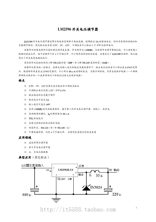
LM2596 开关电压调节器是降压型电源管理单片集成电路,能够输出 3A 的驱动电流,同时具有很好的线性和 负载调节特性。固定输出版本有 3.3V、5V、12V, 可调版本可以输出小于 37V 的各种电压。
该器件内部集成频率补偿和固定频率发生器,开关频率为 150KHz,与低频开关调节器相比较,可以使用更小 规格的滤波元件。由于该器件只需 4 个外接元件,可以使用通用的标准电感,这更优化了 LM2596 的使用,极大地 简化了开关电源电路的设计。
5
TO-263 封装(S)尺寸图
单位:英寸/毫米
TO-220 封装(T)尺寸图
单位:英寸/毫米
6
设计步骤及实例
固定输出调节器的设计步骤
条件:VOUT=3.3(或 5 、或 12)V , VIN(max)为最大直流输入电压, ILOAD(max)为最大负载电流 步骤: 1. 电感的选择(L1) A. 要根据图 4、图 5 和图 6 所示的数据选择电感的适当值(分别对应输出电压为 3.3V、5V 和 12V),对于所有的
R1----1K,1%
D1----5A/40V IN5825 L1---68μH
CFF----参照有关的应用信息
图 1 标准测试电路
在开关调节器中,PCB 版面布局图非常重要,开关电流与环线电感密切相关,由这种环线电感所产生的暂态电 压往往会引起许多问题。要使这种感应最小、地线形成回路,图中所示的粗线部分在 PCB 板上要印制得宽一点,且 要尽可能地短。为了取得最好的效果,外接元器件要尽可能地靠近开关型集成电路,最好用地线屏蔽或单点接地。 最好使用磁屏蔽结构的电感器,如果所用电感是磁芯开放式的,那么,对它的位置必须格外小心。如果电感通量和 敏感的反馈线相交叉,则集成电路的地线及输出端的电容 COUT 的连线可能会引起一些问题。在输出可调的方案 中,必须特别注意反馈电阻及其相关导线的位置。在物理上,一方面电阻要靠近 IC,另一方面相关的连线要远离电 感,如果所用电感是磁芯开放式的,那么,这一点就显得更加重要。
lm2596-3.3__LM2596-ADJ_LM2596-12_LV2596-3.3_中文资料

见注 9
5 10
mA mA(max)
ISTBY
待机静电流
ON/OFF 脚=5V(OFF)(9)
80
μA
200/250
μA(max)
3
符号
参量
条件
θJC
θJA
θJA
热阻
θJA
θJA
ON/OFF 控制 ( 测试电路见图 1)
TO-220 或 TO-263 TO-263(10) TO-263(11) TO-263(12) TO-263(13)
V V(max)
最大工作周期(ON) DC
最小工作周期(OFF)
见注 7 见注 8
100
%
0
%
ICL
极限电流
峰值电流(6,7)
4.5 3.6/3.4
A A(min)
6.9/7.5
A(max)
输出为 0V(6,8)
50
μA(max)
IL
输出漏电流
输出为-1V(9)
2 30
mA mA(max)
IQ
静电流
特点
※ 3.3V、5V、12V 的固定电压输出和可调电压输出 ※ 可调输出电压范围 1.2V~37V±4% ※ 输出线性好且负载可调节 ※ 输出电流可高达 3A ※ 输入电压可高达 40V ※ 采用 150KHz 的内部振荡频率,属于第二代开关电压调节器,功耗小、效率高 ※ 低功耗待机模式,IQ 的典型值为 80μA ※ TTL 断电能力 ※ 具有过热保护和限流保护功能 ※ 封装形式:TO-220(T)和 TO-263(S) ※ 外围电路简单,仅需 4 个外接元件, 且使用容易购买的标准电感
ON/OFF 脚逻辑输入
LM2596的使用
※ 3.3V、5V、12V 的固定电压输出和可调电压输出 ※ 可调输出电压范围 1.2V~37V±4% ※ 输出线性好且负载可调节 ※ 输出电流可高达 3A ※ 输入电压可高达 40V ※ 采用 150KHz 的内部振荡频率,属于第二代开关电压调节器,功耗小、效率高 ※ 低功耗待机模式,IQ 的典型值为 80μA ※ TTL 断电能力 ※ 具有过热保护和限流保护功能 ※ 封装形式:TO-220(T)和 TO-263(S) ※ 外围电路简单,仅需 4 个外接元件, 且使用容易购买的标准电感
ON/OFF 脚逻辑输入
VIH
门槛电压
VIL
低(调节器开) 高(调节器关)
IH
ON/OFF 脚输入电流 IL
VLOGIC=2.5V(调节器关) VLOGIC=0.5V(调节器开)
LM2596□—XX
典型值(2) 极限值(3)
单位
2
℃/W
50
℃/W
50
℃/W
30
℃/W
20
℃/W
1.3
V
0.6
V(max)
纹波滤波电路
注:反馈线要远离电感,电路中的粗线一定要短,最好用地线屏蔽,调节输出电压的电阻 R1、R2 要靠近 LM2596 的 4 脚。
输出电压的计算可由下式给出:
, 其中 VREF=1.23V,
,为了确保输出稳定, R1 选用标称阻值为 1KΩ,精度为 1%的电阻。
CIN---470μF/50V COUT----220μF/35V
A(max) μA(max)
2
mA
30
mA(max)
5
mA
10 80
mA(max) μA
200/250
lm2596中文资料_数据手册_参数
·Regulatorsfrequency卡片上的切换。包括外部关闭,·正到负Convertertypically 80μa 待机电流。自我保护特性包括输出开关的两级频率减少电流限制和完全保护故障状 态下的过热关闭。(1)(1)__专利号5382918。典型应用(固定输出电压版本)请注意,关 于lm2596德州仪器半导体产品和免责lm2596声明的可用性、标准保证和关键应用的 一个重要通知出现在本数据表的末尾。简单切换器是德州仪器的注册商标。所有其 他商标都是其各自所有者的财产。生产数据信息是当前出版日期。版权©1999 - 2013 年,德州仪器IncorporatedProducts符合规格/ TexasInstruments标准保修条款。生产加工 不连接DiagramsFigure 1。5根引线弯曲交错,如图2所示。5-Lead DDPAK/TO-263 (S) PackageThrough Hole TO-220 (T) PackageSee Package Number KTT0005BSee Package Number NDH0005DThese devices have limited内置ESD protection。在储存或处理过程 中,应将引线短接在一起,或将设备置于导电泡沫中,以防止对MOS门的静电损 坏。绝对最大额定参数(1)(2)最大供应Voltage45VON /关销输入电压 0.3 V≤≤+ 25 vfeedback销电压0.3 V≤≤25 + voutput对地电压(稳态) 1 vpower DissipationInternally limitedStorage温度范围 65°C + 150°CESD SusceptibilityHuman身体模型(3)2 kVLead TemperatureDDPAK / - 263 PackageVapor阶段(60秒。)+ 215°CInfrared(10秒)+ 245° 首席技术官- 220包(焊接,10秒)+ 260°CMaximum结温+ 150°C(1)绝对最大额定参数 表明超过这个限制可能发生损坏设备。操作额定值指示设备功能的条件,但不保证 特定的性能限制。(2)如果需lm2596要军用/航空航天专用设备,请与德州仪器销售 办公室/分销商联系,了解其可用性和规格。操作ConditionsTemperature范围 40° C≤TJ≤+ 125°CSupply Voltage4.5V 40 v2submit文档FeedbackCopyright©1999 - 2013年, 德州仪器IncorporatedProduct文件夹链接:LM259图2显示了计时器2自动计数 whenDCEN = 0。在此模式下,bitEXEN2在T2CON中选择两个选项。如果EXEN2 = 0,计时器2计数到0ffh,然后在溢出时设置TF2位。溢出还会导致计时器寄存器被重 新加载,其中包含RCAP2H和RCAP2L中的16位值。捕获ModeRCAP2H和RCAP2L中 的inTimer的值是由软件预先设lm2596定的。如果EXEN2 = 1,那么16位的重载可以 通过溢出或在externalinput T2EX中通过1到0的转换触发。这个转换还设置了EXF2 位。tf2和EXF2位都可以在启用时生成中断。设置DCEN位使定时器2可以向上或向下 计数,如图3所示。在这种模式下,T2EX pin控制了计数的方向。T2EX的逻辑1使计 时器2计数。计时器将在0ffh溢出并设置tf2位。这种溢出还会导致16位值inRCAP2H 和RCAP2L分别被重新加载lm2596到计时器寄存器TH2和TL2中。T2EX的逻辑0使定 时器2倒数。当TH2和TL2等于存储在inRCAP2H和RCAP2L中的值 时,timerunderflows。下流设置TF2位并将0ffh重新加载到计时器寄存器中。EXF2位 可在计时器2溢出或溢出时切换,可lm2596以用作第17位的分辨率。在此操作模式 中,EXF2不标记中断
降压型功率变换器LM2596的原理及应用
第十四届全国电源撞术年会论文集降压型功率变换器LM2596的原理及应用蒋玉萍中国运载火箭技术研究院(100076)摘要:本文介绍降压型功率变换器I.M2596的原理和应用。
叙词弋竖璺兰銮i姆开关电源ADJ。
LM2596控制芯片的工作频率为1501Cttz,其最大电流驱动I引言能力为3A,只需极少量的外围元件就可以实现辟压变换,大大LM7.596系列控制器是美国国家半导体公司推出的降压型开简化了小型开关电源的设计步骤,鳙短了开发周期。
关电源控制芯片,适用于简易高频降压变换器、扳上开关变换2特点和引脚说明器以及正负输出变换器。
该芯片具有四种不同的型号,输出电LM2596采用5脚TO一220(r)和5脚TO一263(s)封装,压分别为3.3v、5.OV、12V和可调输出四种,对应型号分别为:U心孵6T一3.3、删9耵一.5.0、u伫596T—12和U嘶T—如图I所示。
引坤50N,0FF引囊4Feed ma ck引朋3舒锄-d引箨201ln P at}胂l n_图l LM2596引脚封装2.1特点电压信号影响周围的敏感电路,线路板爱锕区需直接与该脚相LM2596系列控制芯片具有以下特点:连。
(1)具有四种不同的输出电压可供选择:3.3V、5.0V、(3)Gnxa,cl(引脚3):信号地。
12V、可调:(4)Feedback(引脚4):输出电压拉测端,构成反馈回路。
(2)可词输出电压范围为1.2v一37V±4%;(5)ON/OFF(引脚5):通过该脚可以控制芯片的工作状(3)最大输出负载驱动电流3A;态。
当滚脚上的电压低于1.3V时,菩片进入工作状态;当该(4)输入电压最高可达40V;脚上的电压高于1.3v时(最高可达到25V),芯片进人睡眠状(5)只需4个外国元件即可实现降压变换;态。
芯片进^睡眠状态后,所需供电电流仅为80,t工A。
如果该引(6)内置150Ⅺb定频振荡器;脚接地或悬空,则睡眠状态被屏蔽,芯片将始终处于工作状态。
LM2596开关电源调节器(中文)
A(max) μA(max)
2
mA
30
mA(max)
5
mA
10 80
mA(max) μA
200/250
μA(max) 3
电子发烧友 电子技术论坛
LM2596 开关电压调节器 SEPTEMBER, 2004
管脚图
极限参数
名称
范围
最大电源电压
45
脚输入电压
-0.3~25
“反馈”脚电压
-0.3~25
到地的输出电压(静态)
-1
功耗
由内部限定
储存温度
-65~150
静电释放(人体放电 1)
2000
气流焊(60 秒)
215
焊接时的管脚
TO-263
红外线焊接(10 秒)
245
温度
TO-220
波峰焊/电烙铁焊接(10 秒)
符号
参量
条件
典型值(2)
极限值(3)
单位
LM2596□—3.3 (见注 14)
VOUT
输出电压
3.3 4.75V≤VIN≤40V,
0.2A≤ILOAD≤3A
η
效率
VIN=12V,ILOAD=3A
Байду номын сангаас73
LM2596□—5.0 (见注 14)
VOUT
输出电压
5.0 7V≤VIN≤40V, 0.2A≤ILOAD≤3A
特点
※ 3.3V、5V、12V 的固定电压输出和可调电压输出 ※ 可调输出电压范围 1.2V~37V±4% ※ 输出线性好且负载可调节 ※ 输出电流可高达 3A ※ 输入电压可高达 40V ※ 采用 150KHz 的内部振荡频率,属于第二代开关电压调节器,功耗小、效率高 ※ 低功耗待机模式,IQ 的典型值为 80μA ※ TTL 断电能力 ※ 具有过热保护和限流保护功能 ※ 封装形式:TO-220(T)和 TO-263(S) ※ 外围电路简单,仅需 4 个外接元件, 且使用容易购买的标准电感
LM2596S-ADJ DCDC电源管理芯片应用资料-奥伟斯
Switching Voltage RegulatorsFeatures∙ 3.3V, 5V, 12V, and adjustable output versions ∙ Adjustable version output voltage range, 1.2V to 37V ± 4% max over line and load conditions ∙ Guaranteed 3A output load current ∙ Input voltage range up to 40V ∙ Requires only 4 external components ∙ Excellent line and load regulation specifications ∙ 150kHz fixed frequency internal oscillator ∙ TTL shutdown capability ∙ Low power standby mode, I Q typically 100μA∙ Thermal shutdown and current limit protectionJM2596-xxTO-220-5LJM2596T-XXTO-263-5LJM2596S-XXORDERING INFORMATIONJM2596S-12 JM2596S-3.3 JM2596S-5.0 JM2596S-ADJ JM2596T-12 JM2596T-3.0 JM2596T-5.0 JM2596T-ADJFunctions∙ Simple high-efficiency step-down regulator ∙ On-card switching regulators ∙ Positive to negative converterDescriptionThe JM2596 series of regulators are monolithic integrated circuits that provide all the active functions for a step-down switching regulator, capable of driving a 3A load with excellent line and load regulation. These devices are available in fixed output voltages of 3.3V, 5V, 12V and an adjustable output version.Requiring a minimum number of external components, these regulators are simple to use.The JM2596 series operates at a switching frequency of 150kHz. Available in standard 5-lead TO-220 package.Other features include a guaranteed ± 4% tolerance on output voltage under specified input voltage and output load conditions, and ± 15% on the oscillator frequency. External shutdown is included, featuring typically 100μA standby current. Self protection features include a two stage frequency reducing current limit for output switch and an over temperature shutdown for completeprotection under fault conditions. The over temperature shutdown level is about 145o C with 5oC hysteresis.说明JM2596系列稳压器是单片集成电路,为降压开关稳压器提供所有的有源功能,能够以优良的线路和负载调节驱动3A负载。
LM2596构成的可调限流稳压器

LM2596构成的可调限流稳压器
LM2596简介
LM2596系列稳压芯片,是德州仪器(TI)生产的3A降压开关型稳压芯片。
LM2596性能特点:
•内含固定频率振荡器(150KHZ)和基准稳压器(1.23v)
•具有完善的保护电路、电流限制、热关断电路等
•仅需极少的外围器件便可构成高效稳压电路
•提供3.3V、5V、12V及可调(-ADJ)等多个电压档次
LM2596构成的可调限流稳压器
LM2596的常规应用,不具备电流限制功能,在一些电子设计和辅助设备上,对限流功能有一定的需求,虽然厂家给出的标准应用电路无法完成这一功能,我们可以通过适当的添加功能电路,让它实现限流功能。
如下图:
LM2596构成的可调限流稳压器
上图的功能网友已经验证过,出于严谨,小编在此不做工作原理的分析,‘机电匠’有机会对电路功能做验证实验的时候,再通过视频文章向大家呈现。
基于32数控dcdc稳压电源代码

基于32数控dcdc稳压电源代码一、介绍32数控DCDC稳压电源是一款高效、稳定的电源模块,可以输出可调的直流电压。
它采用STM32F103C8T6单片机作为控制核心,具有高精度、低噪声等特点。
本文将详细介绍基于32数控DCDC稳压电源代码的实现方法。
二、硬件设计1. 电路原理图32数控DCDC稳压电源的电路原理图如下所示:其中,U1为STM32F103C8T6单片机,U2为LM2675-5.0芯片,用于实现升压转换。
C1、C2为输入滤波电容,C3、C4为输出滤波电容,L1为升压电感。
2. PCB设计根据上述原理图进行PCB设计,并进行布线和焊接。
三、软件设计1. 系统框架本系统采用Keil MDK-ARM开发工具进行编程开发。
系统框架如下所示:其中,main.c为主程序文件,包括系统初始化和主循环函数;system.c和system.h文件包含了系统时钟配置和中断处理函数;adc.c和adc.h文件包含了ADC采样函数;pwm.c和pwm.h文件包含了PWM输出函数;lcd.c和lcd.h文件包含了LCD显示函数。
2. 系统初始化系统初始化包括时钟配置、GPIO配置、ADC配置、PWM配置和LCD配置等。
其中,时钟配置采用外部晶振8MHz,系统时钟频率为72MHz;GPIO配置包括输入口和输出口的初始化;ADC采样使用单通道模式,采样时间为239.5个周期,分辨率为12位;PWM输出使用TIM3定时器,频率为20kHz,占空比可调;LCD显示使用4位并行接口方式,液晶屏型号为1602A。
3. 主循环函数主循环函数包括ADC采样、电压计算、PID控制和PWM输出等功能。
具体实现方法如下:(1)ADC采样:通过调用adc.c文件中的函数进行单次ADC采样,并将结果存储在变量中。
(2)电压计算:根据ADC采样结果计算实际输出电压值,并与设定值进行比较。
(3)PID控制:根据实际输出电压值与设定值之差计算PID控制器的输出值,并限制其范围在0-100之间。
LM2596S资料

LM2596系列是美国国家半导体公司生产的3A电流输出降压开关型集成稳压芯片,它内含固定频率振荡器(150KHZ)和基准稳压器(1.23v),并具有完善的保护电路、电流限制、热关断电路等。
利用该器件只需极少的外围器件便可构成高效稳压电路。
提供的有:3.3V、5V、12V及可调(-ADJ)等多个电压档次产品。
此外,该芯片还提供了工作状态的外部控制引脚。
LM2596系列开关稳压集成电路的主要特性如下:1、最大输出电流:3A2、最高输出电压:37V3、输出电压:3.3V、5V、12V及(ADJ)等,最大输出电压37V4、震荡频率:150KHZ5、转换效率:75%~88%(不同电压输出时的转换效率不同)6、工作温度范围:-40℃~+125℃7、工作模式:低功耗/正常两种模式。
可外部控制8、工作模式控制:TTL电平相容9、所需外部组件:仅四个(不可调);六个(可调)10、器件保护:热关断及电流限制11、封装形式:5脚(TO-220(T);TO-263(S))LM2596芯片内部框图。
注:此图为TO-220封装形式的内部框图。
LM2596内部包含150KHZ振荡器、1.23v基准稳压电路、热关断电路、电流限制电路、放大器、比较器和内部稳压电路等。
为了产生不同的输出电压通常将比较器的负端接基准电压(1.23V ),正端接分压电阻网络。
其中R1=1KΩ ,R2分别为1.7KΩ (3.3v),3.1KΩ(5V),8.8KΩ (12V)、0(-ADJ)。
将输出电压的分压电阻网络的输出同内部基准稳压值1.23V进行比较,若电压有偏差,则可用放大器控制内部振荡器的输出占空比,从而使输出电压保持稳定。
3应用实例具体应用时可根据需要选择:LM2596可调电压型、LM2596-5V、LM2596-3.3等定压输出型。
要获得+1.8V 输出电压时请选用A图,要获得+3.3V、+5V输出电压时请选用B图。
4散热问题LM2596有两种封装形式,5脚TO-220(T);TO-263(S)。
开关型稳压芯片LM2576中文资料之欧阳法创编

开关型稳压芯片LM2576中文资料LM2576系列开关稳压集成电路是线性三端稳压器件(如78xx系列端稳压集成电路)的替代品,它具有可靠的工作性能、较高的工作效率和较强的输出电流驱动能力,从而为MCU的稳定、可靠工作提供了强有力的保证。
LM2576简介LM2576系列是美国国家半导体公司生产的3A电流输出降压开关型集成稳压电路,它内含固定频率振荡器(52kHz)和基准稳压器(1.23V),并具有完善的保护电路,包括电流限制及热关断电路等,利用该器件只需极少的外围器件便可构成高效稳压电路。
LM2576系列包括LM2576(最高输入电压40V)及LM2576HV(最高输入电压60V)二个系列。
各系列产品均提供有3.3V(-3.3)、5V(-5.0)、12V(-12)、15V(-15)及可调(-ADJ)等多个电压档次产品。
此外,该芯片还提供了工作状态的外部控制引脚。
LM2576系列开关稳压集成电路的主要特性如下[2]:●最大输出电流:3A;●最高输入电压:LM2576为40V,LM2576HV为60V;●输出电压:3.3V、5V、12V、15V和ADJ(可调)等可选;●振东频率:52kHz;●转换效率:75%~88%(不同电压输出时的效率不同);●控制方式:PWM;●工作温度范围:-40℃~+125℃●工作模式:低功耗/正常两种模式可外部控制;●工作模式控制:TTL电平兼容;●所需外部元件:仅四个(不可调)或六个(可调);●器件保护:热关断及电流限制;●封装形式:TO-220或TO-263。
LM2576的内部框图如图1所示,该框图的引脚定义对应于五脚TO-220封装形式。
LM2576内部包含52kHz振荡器、1.23V基准稳压电路、热关断电路、电流限制电路、放大器、比较器及内部稳压电路等。
为了产生不同的输出电压,通常将比较器的负端接基准电压(1.23V),正端接分压电阻网络,这样可根据输出电压的不同选定不同的阻值,其中R1=1kΩ(可调-ADJ时开路),R2分别为 1.7 kΩ(3.3V)、3.1 kΩ(5V)、8.84 kΩ(12V)、11.3 kΩ(15V)和0(-ADJ),上述电阻依据型号不同已在芯片内部做了精确调整,因而无需使用者考虑。
LM2596S-3.3-3A降压电压稳压器应用方案

随着科学技术的发展进步,电子元器逐渐智能化,多样化,应用的范围也越来越广泛。
LM2596系列:3A电流输出降压开关型集成稳压芯片,它内含固定频率振荡器(150KHZ),和基准稳压器(1.23v),并具有完善的保护电路:电流限制、热关断电路等。
利用该器件只需极少的外围器件便可构成高效稳压电路。
提供有:3.3V、5V、12V及可调(-ADJ)等多个电压档次产品。
深圳市奥伟斯科技有限公司是一家专注触摸芯片,单片机,电源管理芯片,语音芯片,场效应管,显示驱动芯片,网络接收芯片,运算放大器,红外线接收头及其它半导体产品的研发,代理销售推广的高新技术企业.奥伟斯科技自成立以来一直致力于新半导体产品在国内的推广与销售,年销售额超过壹亿人民币是一家具有综合竞争优势的专业电子元器件代理商.本公司代理推广的一系列优秀触摸芯片及语音芯片,现以大批量应用到智能电子锁、饮水机、电饭煲、LED台灯等控制器为顾客提供最佳解决方案,受到广大客户的一致赞誉。
奥伟斯科技优势行业集中在家用电器和汽车电子领域,包括:智能电子锁、饮水机、抽烟机、空调、洗衣机、冰箱、洗碗机、电饭煲、电磁炉、微波炉、电动自行车、汽车仪表、汽车音响、汽车空调等。
销售网络覆盖华东、华南及华北地区。
奥伟斯科技已为众多世界著名企业提供服务如:美的、小米、云米、长虹、创维、三星、LG、飞利浦、TCL、海尔、美菱、沁园、等众多中国一流品牌电家厂商奥伟斯科技提供专业的智能电子锁触摸解决方案,并提供电子锁整套的芯片配套:低功耗触摸芯片低功耗单片机马达驱动芯片显示驱动芯片刷卡芯片时针芯片存储芯片语音芯片低压MOS管 TVS二极管主要品牌产品:OWEIS-TECHOWEIS触摸芯片 OWEIS接口芯片 OWEIS电源芯片 OWEIS语音芯片 OWEIS场效应管一.电容式触摸芯片ADSEMI触摸芯片代理芯邦科技触控芯片万代科技触摸按键芯片博晶微触摸控制芯片海栎创触摸感应芯片启攀微触摸IC 融和微触摸感应IC 合泰触摸按键IC 通泰触摸芯片二.汽车电子/电源管理/接口芯片/逻辑芯片:IKSEMICON一级代理 ILN2003ADT IK62783DT IL2596 IL2576 ILX485 ILX3485ILX232 ILX3232三.功率器件/接收头/光电开关:KODENSHI AUK SMK系列MOS管SMK0260F SMK0460F SMK0760F SMK1260F SMK1820F SMK18T50F四. LED显示驱动芯片:中微爱芯AIP系列 AIP1668 AIP1628 AIP1629 AIP1616天微电子TM系列 TM1628 TM1668 TM1621五.电源管理芯片:Power Integrations LNK364PN LNK564PN 芯朋微PN8012 PN8015 AP5054 AP5056 力生美晶源微友达天钰电子FR9886 FR9888六.语音芯片:APLUS巨华电子AP23085 AP23170 AP23341 AP23682 AP89085 AP89170 AP89341 AP89341K AP89682七.运算放大器:3PEAK运算放大器聚洵运算放大器圣邦微运算放大器八.发光二极管:OSRAM欧司朗发光二极管 Lite-On光宝发光二极管 Everlight亿光发光二极管Kingbright今台发光二极管九. CAN收发器:NXP恩智浦CAN收发器 Microchip微芯CAN收发器十.分销产品线:ONSEMI安森美 TI德州仪器 ADI TOSHIBA东芝 AVAGO安华高十一 MCU单片机ABOV现代单片机MC96F系列 Microchip微芯单片机PIC12F PIC16F PIC18F系列FUJITSU富仕通单片机MB95F系列 STM单片机STM32F STM32L系列 CKS中科芯单片机CKS32F系列 TI单片机MSP430系列 TMS320F系列 NXP单片机LPC系列LM2596SNVS124C – NOVEMBER 1999 – REVISED APRIL 2013LM2596 SIMPLE SWITCHER ® Power Converter 150 kHz3A Step-Down Voltage RegulatorCheck for Samples: LM2596FEATURESDESCRIPTION• 3.3V, 5V, 12V, and Adjustable Output Versions • Adjustable Version Output Voltage Range,1.2V to 37V ±4% Max Over Line and Load The LM2596 series of regulators are monolithic integrated circuits that provide all the active functions for a step-down (buck) switching regulator, capable of driving a 3A load with excellent line and loadConditionsregulation. These devices are available in fixed output • Available in TO-220 and TO-263 Packages • Ensured 3A Output Load Current • Input Voltage Range Up to 40V• Requires Only 4 External Components voltages of 3.3V, 5V, 12V, and an adjustable output version.Requiring a minimum number of external components, these regulators are simple to use and include internal frequency compensation , and a • Excellent Line and Load Regulationfixed-frequency oscillator.Specifications• 150 kHz Fixed Frequency Internal Oscillator The LM2596 series operates at a switching frequency of 150 kHz thus allowing smaller sized filter • TTL Shutdown Capabilitycomponents than what would be needed with lower • Low Power Standby Mode, I Q Typically 80 μA • High Efficiencyfrequency switching regulators. Available in a standard 5-lead TO-220 package with several different lead bend options, and a 5-lead TO-263 • Uses Readily Available Standard Inductors surface mount package.• Thermal Shutdown and Current Limit A standard series of inductors are available from Protectionseveral different manufacturers optimized for use with the LM2596 series. This feature greatly simplifies the APPLICATIONSdesign of switch-mode power supplies.• Simple High-Efficiency Step-Down (Buck)Other features include a ensured ±4% tolerance on Regulatoroutput voltage under specified input voltage and • On-Card Switching Regulators • Positive to Negative ConverterTypical Application(Fixed Output Voltage Versions)output load conditions, and ±15% on the oscillator frequency. External shutdown is included, featuring typically 80 μA standby current. Self protection features include a two stage frequency reducing current limit for the output switch and an over temperature shutdown for complete protection under fault conditions. (1)(1) † Patent Number 5,382,918.Please be aware that an important notice concerning availability, standard warranty, and use in critical applications of Texas Instruments semiconductor products and disclaimers thereto appears at the end of this data sheet.SIMPLE SWITCHER is a registered trademark of Texas Instruments. All other trademarks are the property of their respective owners.PRODUCTION DATA information is current as of publication date. Copyright © 1999–2013, Texas Instruments IncorporatedProducts conform to specifications per the terms of the Texas Instruments standard warranty. Production processing does notnecessarily include testing of all parameters.Connection DiagramsFigure 1. 5-Lead Bent and Staggered Leads, Figure 2. 5-Lead DDPAK/TO-263 (S) Package Through Hole TO-220 (T) Package See Package Number KTT0005BSee Package Number NDH0005DThese devices have limited built-in ESD protection. The leads should be shorted together or the device placed in conductive foam during storage or handling to prevent electrostatic damage to the MOS gates.(1)(2)(1) Absolute Maximum Ratings indicate limits beyond which damage to the device may occur. Operating Ratings indicate conditions forwhich the device is intended to be functional, but do not ensure specific performance limits. For ensured specifications and test conditions, see the Electrical Characteristics.(2) If Military/Aerospace specified devices are required, please contact the Texas Instruments Sales Office/ Distributors for availability andspecifications.(3) The human body model is a 100 pF capacitor discharged through a 1.5k resistor into each pin.Specifications with standard type face are for T J = 25°C, and those with boldface type apply over full Operating(1) Typical numbers are at 25°C and represent the most likely norm.(2) All limits specified at room temperature (standard type face) and at temperature extremes (bold type face). All room temperature limitsare 100% production tested. All limits at temperature extremes are ensured via correlation using standard Statistical Quality Control (SQC) methods. All limits are used to calculate Average Outgoing Quality Level (AOQL).(3) External components such as the catch diode, inductor, input and output capacitors, and voltage programming resistors can affectswitching regulator system performance. When the LM2596 is used as shown in the Figure 20 test circuit, system performance will be as shown in system parameters of Electrical Characteristics section.LM2596-5.0 Electrical CharacteristicsSpecifications with standard type face are for T J = 25°C, and those with boldface type apply over full Operating(1) Typical numbers are at 25°C and represent the most likely norm.(2) All limits specified at room temperature (standard type face) and at temperature extremes (bold type face). All room temperature limitsare 100% production tested. All limits at temperature extremes are ensured via correlation using standard Statistical Quality Control (SQC) methods. All limits are used to calculate Average Outgoing Quality Level (AOQL).(3) External components such as the catch diode, inductor, input and output capacitors, and voltage programming resistors can affectswitching regulator system performance. When the LM2596 is used as shown in the Figure 20 test circuit, system performance will be as shown in system parameters of Electrical Characteristics section.LM2596-12 Electrical CharacteristicsSpecifications with standard type face are for T J = 25°C, and those with boldface type apply over full Operating(1) Typical numbers are at 25°C and represent the most likely norm.(2) All limits specified at room temperature (standard type face) and at temperature extremes (bold type face). All room temperature limitsare 100% production tested. All limits at temperature extremes are ensured via correlation using standard Statistical Quality Control (SQC) methods. All limits are used to calculate Average Outgoing Quality Level (AOQL).(3) External components such as the catch diode, inductor, input and output capacitors, and voltage programming resistors can affectswitching regulator system performance. When the LM2596 is used as shown in the Figure 20 test circuit, system performance will be as shown in system parameters of Electrical Characteristics section.Specifications with standard type face are for T J = 25°C, and those with boldface type apply over full Operating(1) Typical numbers are at 25°C and represent the most likely norm.(2) All limits specified at room temperature (standard type face) and at temperature extremes (bold type face). All room temperature limitsare 100% production tested. All limits at temperature extremes are ensured via correlation using standard Statistical Quality Control (SQC) methods. All limits are used to calculate Average Outgoing Quality Level (AOQL).(3) External components such as the catch diode, inductor, input and output capacitors, and voltage programming resistors can affectswitching regulator system performance. When the LM2596 is used as shown in the Figure 20 test circuit, system performance will be as shown in system parameters of Electrical Characteristics section.All Output Voltage Versions Electrical CharacteristicsSpecifications with standard type face are for T J = 25°C, and those with boldface type apply over full Operating Temperature Range. Unless otherwise specified, V IN = 12V for the 3.3V, 5V, and Adjustable version and V IN = 24V for the(1) Typical numbers are at 25°C and represent the most likely norm.(2) All limits specified at room temperature (standard type face) and at temperature extremes (bold type face). All room temperature limitsare 100% production tested. All limits at temperature extremes are ensured via correlation using standard Statistical Quality Control (SQC) methods. All limits are used to calculate Average Outgoing Quality Level (AOQL).(3) The switching frequency is reduced when the second stage current limit is activated.(4) No diode, inductor or capacitor connected to output pin.(5) Feedback pin removed from output and connected to 0V to force the output transistor switch ON.(6) Feedback pin removed from output and connected to 12V for the 3.3V, 5V, and the ADJ. version, and 15V for the 12V version, to forcethe output transistor switch OFF.(7) V IN = 40V.All Output Voltage Versions Electrical Characteristics (continued)Specifications with standard type face are for T J = 25°C, and those with boldface type apply over full Operating Temperature Range. Unless otherwise specified, V IN = 12V for the 3.3V, 5V, and Adjustable version and V IN = 24V for the(8) Junction to ambient thermal resistance (no external heat sink) for the TO-220 package mounted vertically, with the leads soldered to aprinted circuit board with (1 oz.) copper area of approximately 1 in2.(9) Junction to ambient thermal resistance with the TO-263 package tab soldered to a single printed circuit board with 0.5 in2 of (1 oz.)copper area.(10) Junction to ambient thermal resistance with the TO-263 package tab soldered to a single sided printed circuit board with 2.5 in2 of (1oz.) copper area.(11) Junction to ambient thermal resistance with the TO-263 package tab soldered to a double sided printed circuit board with 3 in2 of (1 oz.)copper area on the LM2596S side of the board, and approximately 16 in2 of copper on the other side of the p-c board. See Application Information in this data sheet and the thermal model in Switchers Made Simple™ version 4.3 software.Typical Performance Characteristics(Circuit of Figure 20)NormalizedOutput Voltage Line RegulationFigure 3. Figure 4.Switch Saturation Efficiency VoltageFigure 5. Figure 6.Switch Current Limit Dropout VoltageFigure 7. Figure 8.(Circuit of Figure 20)Operating ShutdownQuiescent Current Quiescent CurrentFigure 9. Figure 10.Minimum Operating ON /OFF ThresholdSupply Voltage VoltageFigure 11. Figure 12.ON /OFF PinCurrent (Sinking) Switching FrequencyFigure 13. Figure 14.(Circuit of Figure 20)Continuous Mode Switching WaveformsFeedback Pin V IN = 20V, V OUT = 5V, I LOAD = 2ABias CurrentL = 32 μH, C OUT = 220 μF, C OUT ESR = 50 mΩA: Output Pin Voltage, 10V/div. B: Inductor Current 1A/div.C: Output Ripple Voltage, 50 mV/div.Figure 15.Figure 16. Horizontal Time Base: 2 μs/div.Discontinuous Mode Switching WaveformsLoad Transient Response for Continuous Mode V IN = 20V, V OUT = 5V, I LOAD = 500 mAV IN = 20V, V OUT = 5V, I LOAD = 500 mA to 2A L = 10 μH, C OUT = 330 μF, C OUT ESR = 45 mΩL = 32 μH, C OUT = 220 μF, C OUT ESR = 50 mΩA: Output Pin Voltage, 10V/div. B: Inductor Current 0.5A/div.C: Output Ripple Voltage, 100 mV/div.A: Output Voltage, 100 mV/div. (AC) B: 500 mA to 2A Load PulseFigure 17. Horizontal Time Base: 2 μs/div.Figure 18. Horizontal Time Base: 100 μs/div.Load Transient Response for Discontinuous ModeV IN = 20V, V OUT = 5V, I LOAD = 500 mA to 2A L = 10 μH, C OUT = 330 μF, C OUT ESR = 45 mΩA: Output Voltage, 100 mV/div. (AC) B: 500 mA to 2A Load PulseFigure 19. Horizontal Time Base: 200 μs/div.Test Circuit and Layout GuidelinesFixed Output Voltage VersionsC IN —470 μF, 50V, Aluminum Electrolytic Nichicon “PL Series” C OUT —220 μF, 25V Aluminum Electrolytic, Nichicon “PL Series” D1 —5A, 40V Schottky Rectifier, 1N5825 L1 —68 μH, L38where V REF = 1.23VAdjustable Output Voltage VersionsSelect R 1 to be approximately 1 kΩ, use a 1% resistor for best stability. C IN —470 μF, 50V, Aluminum Electrolytic Nichicon “PL Series” C OUT —220 μF, 35V Aluminum Electrolytic, Nichicon “PL Series” D1 —5A, 40V Schottky Rectifier, 1N5825 L1 —68 μH, L38 R1 —1 kΩ, 1%C FF —See Application Information SectionFigure 20. Standard Test Circuits and Layout GuidesAs in any switching regulator, layout is very important. Rapidly switching currents associated with wiring inductance can generate voltage transients which can cause problems. For minimal inductance and ground loops, the wires indicated by heavy lines should be wide printed circuit traces and should be kept as short as possible. For best results, external components should be located as close to the switcher lC as possible using ground plane construction or single point grounding.If open core inductors are used, special care must be taken as to the location and positioning of this type of inductor. Allowing the inductor flux to intersect sensitive feedback, lC groundpath and C OUT wiring can cause problems.When using the adjustable version, special care must be taken as to the location of the feedback resistors and the associated wiring. Physically locate both resistors near the IC, and route the wiring away from the inductor, especially an open core type of inductor. (See Application Information section for moreinformation.)LM2596 Series Buck Regulator Design Procedure (Fixed Output)Table 1. LM2596 Fixed Voltage Quick Design Component Selection TableTable 1. LM2596 Fixed Voltage Quick Design Component Selection Table (continued)LM2596 Series Buck Regulator Design Procedure (Adjustable Output)= 1k (16.26 − 1) = 15.26k, closest 1% value is 15.4 kΩ. = 15.4 kΩ. Select a value for R 1 between 240Ω and 1.5 kΩ. The lower resistor values minimize noise pickup in the sensitive feedback pin. (For the temperature coefficient and the best stability 1% metal film resistors.)(2)2. Inductor Selection (L1)A. Calculate the inductor Volt • microsecond constant E • T (V • μs), from the following formula:where•V SAT = internal switch saturation voltage =1.16V•V D = diode forward voltage drop = 0.5V (4) B. Use the E • T value from the previous formula and match it with the E • T number on the vertical axis of the Inductor Value Selection Guide shown in Figure 24.C. on the horizontal axis, select the maximum load current.D. Identify the inductance region intersected by the E • T value and the Maximum Load Current value. Each region is identified by an inductance value and an inductor code (LXX).E. Select an appropriate inductor from the four manufacturer's part numbers listed in Table 3.E • T = 34.2 (V • μs)LOAD(max) = 3AFrom the inductor value selection guide shown ininductance region intersected by the 34 (V • μs) horizontalthe 3A vertical line is 47 μH, and the inductor code isFrom the table in Table 3, locate line L39, and select an inductor part number from the list of manufacturers part numbers.3. Output Capacitor SeIection (C OUT)See section on C OUT in Application Information section.From the quick design table shown in Table 2, locatevoltage column. From that column, locate the output voltage closest4. Feedforward Capacitor (C FF) (See Figure 20)For output voltages greater than approximately 10V, an additional capacitor is required. The compensation capacitor is typically between 100 pF and 33 nF, and is wired in parallel with the output voltage setting resistor, R2. It provides additional stability for high output voltages, low input-output voltages, and/or very low ESR output capacitors, such as solid tantalum capacitors.(6) This capacitor type can be ceramic, plastic, silver mica, etc. (Because of the unstable characteristics of ceramic capacitors made with Z5U material, they are not recommended.)LM2596 Series Buck Regulator Design Procedure (Adjustable Output)Table 2. Output Capacitor and Feedforward Capacitor Selection TableTable 2. Output Capacitor and Feedforward Capacitor Selection Table (continued)LM2596 Series Buck Regulator Design ProcedureINDUCTOR VALUE SELECTION GUIDES(For Continuous Mode Operation)Figure 21. LM2596-3.3 Figure 22. LM2596-5.0Figure 23. LM2596-12 Figure 24. LM2596-ADJTable 3. Inductor Manufacturers Part NumbersTable 4. Inductor Manufacturers Phone NumbersTable 5. Capacitor Manufacturers Phone NumbersTable 5. Capacitor Manufacturers Phone Numbers (continued)Table 6. Diode Selection TableBlock DiagramAPPLICATION INFORMATIONTable 7. PIN DESCRIPTIONSEXTERNAL COMPONENTSINPUT CAPACITORC IN—A low ESR aluminum or tantalum bypass capacitor is needed between the input pin and ground pin. It must be located near the regulator using short leads. This capacitor prevents large voltage transients from appearing at the input, and provides the instantaneous current needed each time the switch turns on.The important parameters for the Input capacitor are the voltage rating and the RMS current rating. Because of the relatively high RMS currents flowing in a buck regulator's input capacitor, this capacitor should be chosen for its RMS current rating rather than its capacitance or voltage ratings, although the capacitance value and voltage rating are directly related to the RMS current rating.The RMS current rating of a capacitor could be viewed as a capacitor's power rating. The RMS current flowing through the capacitors internal ESR produces power which causes the internal temperature of the capacitor to rise. The RMS current rating of a capacitor is determined by the amount of current required to raise the internal temperature approximately 10°C above an ambient temperature of 105°C. The ability of the capacitor to dissipate this heat to the surrounding air will determine the amount of current the capacitor can safely sustain. Capacitors that are physically large and have a large surface area will typically have higher RMS current ratings. For a given capacitor value, a higher voltage electrolytic capacitor will be physically larger than a lower voltage capacitor, and thus be able to dissipate more heat to the surrounding air, and therefore will have a higher RMS current rating. The consequences of operating an electrolytic capacitor above the RMS current rating is a shortened operating life. The higher temperature speeds up the evaporation of the capacitor's electrolyte, resulting in eventual failure. Selecting an input capacitor requires consulting the manufacturers data sheet for maximum allowable RMS ripple current. For a maximum ambient temperature of 40°C, a general guideline would be to select a capacitor with a ripple current rating of approximately 50% of the DC load current. For ambient temperatures up to 70°C, a current rating of 75% of the DC load current would be a good choice for a conservative design. The capacitor voltage rating must be at least 1.25 times greater than the maximum input voltage, and often a much higher voltage capacitor is needed to satisfy the RMS current requirements.A graph shown in Figure 25 shows the relationship between an electrolytic capacitor value, its voltage rating, and the RMS c urrent it is rated for. These curves were obtained from the Nichicon “PL” series of low ESR, high reliability electrolytic capacitors designed for switching regulator applications. Other capacitor manufacturers offer similar types of capacitors, but always check the capacitor data sheet.“Standard” electrolytic capacitors typically have much higher ESR numbers, lower RMS current ratings and typically have a shorter operating lifetime.Because of their small size and excellent performance, surface mount solid tantalum capacitors are often used for input bypassing, but several precautions must be observed. A small percentage of solid tantalum capacitors can short if the inrush current rating is exceeded. This can happen at turn on when the input voltage is suddenly applied, and of course, higher input voltages produce higher inrush currents. Several capacitor manufacturers do a 100% surge current testing on their products to minimize this potential problem. If high turn on currents are expected, it may be necessary to limit this current by adding either some resistance or inductance before the tantalum capacitor, or select a higher voltage capacitor. As with aluminum electrolytic capacitors, the RMS ripple current rating must be sized to the load current.FEEDFORWARD CAPACITOR(Adjustable Output Voltage Version)C FF— A Feedforward Capacitor C FF, shown across R2 in Figure 20 is used when the ouput voltage is greater than 10V or when C OUT has a very low ESR. This capacitor adds lead compensation to the feedback loop and increases the phase margin for better loop stability. For C FF selection, see the Design Procedure section.Figure 25. RMS Current Ratings for Low ESR Electrolytic Capacitors (Typical)OUTPUT CAPACITORC OUT— An output capacitor is required to filter the output and provide regulator loop stability. Low impedance or low ESR Electrolytic or solid tantalum capacitors designed for switching regulator applications must be used. When selecting an output capacitor, the important capacitor parameters are; the 100 kHz Equivalent Series Resistance (ESR), the RMS ripple current rating, voltage rating, and capacitance value. For the output capacitor, the ESR value is the most important parameter.The output capacitor requires an ESR value that has an upper and lower limit. For low output ripple voltage, a low ESR value is needed. This value is determined by the maximum allowable output ripple voltage, typically 1% to 2% of the output voltage. But if the selected capacitor's ESR is extremely low, there is a possibility of an unstable feedback loop, resulting in an oscillation at the output. Using the capacitors listed in the tables, or similar types, will provide design solutions under all conditions.If very low output ripple voltage (less than 15 mV) is required, refer to the section on OUTPUT VOLTAGE RIPPLE AND TRANSIENTS for a post ripple filter.An aluminum electrolytic capacitor's ESR value is related to the capacitance value and its voltage rating. In most cases, higher voltage electrolytic capacitors have lower ESR values (see Figure 26 ). Often, capacitors with much higher voltage ratings may be needed to provide the low ESR values required for low output ripple voltage. The output capacitor for many different switcher designs often can be satisfied with only three or four different capacitor values and several different voltage ratings. See the quick design component selection tables in Table 1 and 4 for typical capacitor values, voltage ratings, and manufacturers capacitor types.Electrolytic ca pacitors are not recommended for temperatures below −25°C. The ESR rises dramatically at cold temperatures and typically rises 3X @ −25°C and as much as 10X at −40°C. See curve shown in Figure 27.Solid tantalum capacitors have a much better ESR spec for cold temperatures and are recommended for temperatures below −25°C.Figure 26. Capacitor ESR vs Capacitor Voltage Rating (Typical Low ESR Electrolytic Capacitor)CATCH DIODEBuck regulators require a diode to provide a return path for the inductor current when the switch turns off. This must be a fast diode and must be located close to the LM2596 using short leads and short printed circuit traces. Because of their very fast switching speed and low forward voltage drop, Schottky diodes provide the best performance, especially in low output voltage applications (5V and lower). Ultra-fast recovery, or High-Efficiency rectifiers are also a good choice, but some types with an abrupt turnoff characteristic may cause instability or EMI problems. Ultra-fast recovery diodes typically have reverse recovery times of 50 ns or less. Rectifiers such as the 1N5400 series are much too slow and should not be used.Figure 27. Capacitor ESR Change vs TemperatureINDUCTOR SELECTIONAll switching regulators have two basic modes of operation; continuous and discontinuous. The difference between the two types relates to the inductor current, whether it is flowing continuously, or if it drops to zero for a period of time in the normal switching cycle. Each mode has distinctively different operating characteristics, which can affect the regulators performance and requirements. Most switcher designs will operate in the discontinuous mode when the load current is low.The LM2596 (or any of the Simple Switcher family) can be used for both continuous or discontinuous modes of operation.In many cases the preferred mode of operation is the continuous mode. It offers greater output power, lower peak switch, inductor and diode currents, and can have lower output ripple voltage. But it does require larger inductor values to keep the inductor current flowing continuously, especially at low output load currents and/or high input voltages.To simplify the inductor selection process, an inductor selection guide (nomograph) was designed (see Figure 21 through 8). This guide assumes that the regulator is operating in the continuous mode, and selects an inductor that will allow a peak-to-peak inductor ripple current to be a certain percentage of the maximum design load current. This peak-to-peak inductor ripple current percentage is not fixed, but is allowed to change as different design load currents are selected. (See Figure 28.)Figure 28. (ΔI IND) Peak-to-Peak InductorRipple Current (as a Percentage of the Load Current)vs Load CurrentBy allowing the percentage of inductor ripple current to increase for low load currents, the inductor value and size can be kept relatively low.When operating in the continuous mode, the inductor current waveform ranges from a triangular to a sawtooth type of waveform (depending on the input voltage), with the average value of this current waveform equal to the DC output load current.Inductors are available in different styles such as pot core, toroid, E-core, bobbin core, etc., as well as different core materials, such as ferrites and powdered iron. The least expensive, the bobbin, rod or stick core, consists of wire wound on a ferrite bobbin. This type of construction makes for an inexpensive inductor, but since the magnetic flux is not completely contained within the core, it generates more Electro-Magnetic Interference (EMl). This magnetic flux can induce voltages into nearby printed circuit traces, thus causing problems with both the switching regulator operation and nearby sensitive circuitry, and can give incorrect scope readings because of induced voltages in the scope probe. Also see section on OPEN CORE INDUCTORS.When multiple switching regulators are located on the same PC board, open core magnetics can cause interference between two or more of the regulator circuits, especially at high currents. A torroid or E-core inductor (closed magnetic structure) should be used in these situations.The inductors listed in the selection chart include ferrite E-core construction for Schott, ferrite bobbin core for Renco and Coilcraft, and powdered iron toroid for Pulse Engineering.Exceeding an inductor's maximum current rating may cause the inductor to overheat because of the copper wire losses, or the core may saturate. If the inductor begins to saturate, the inductance decreases rapidly and the inductor begins to look mainly resistive (the DC resistance of the winding). This can cause the switch current to rise very rapidly and force the switch into a cycle-by-cycle current limit, thus reducing the DC output load current. This can also result in overheating of the inductor and/or the LM2596. Different inductor types have different saturation characteristics, and this should be kept in mind when selecting an inductor.The inductor manufacturer's data sheets include current and energy limits to avoid inductor saturation.。
- 1、下载文档前请自行甄别文档内容的完整性,平台不提供额外的编辑、内容补充、找答案等附加服务。
- 2、"仅部分预览"的文档,不可在线预览部分如存在完整性等问题,可反馈申请退款(可完整预览的文档不适用该条件!)。
- 3、如文档侵犯您的权益,请联系客服反馈,我们会尽快为您处理(人工客服工作时间:9:00-18:30)。
图1 DC/DC 开关稳压器原理框图DC/DC 开关稳压器输出电压:I 阿二(1+与-)x1』 t\ 1其中Vref 为DC/DC 开关稳压器内部自带的基准电压或者用户外接的基准电压, 路,用于设置输出电压的大小。
当输出电压Vout 因负载变化而变化时,反馈电压Vf 也随着变化,DC/DC 稳压基于 LM2596-ADJ DC/DC稳压器的高效率恒流稳压电源设计开关恒流稳压电源LED DC/DC当前全球能源紧缺日益加剧,制约着经济的发展,节能成为人类面临的重要课题。
在照明领域,被称为第 照明光源或绿色光源的 LED 照明产品以节能、环保、寿命长、体积小、坚固耐用等特点吸引着世人的目光。
由于LED 的伏安特性呈现非线性且伏安特性具有负温度系数的特点,以及生产工艺和生产水平的差异,不 同生产厂家生产的同样功率等级的大功率 LED 伏安特性存在差异,即使是同一厂家生产的同一批次的LED ,个 体间的正向压降也存在一定差异等原因,为了减少 LED 的光衰,延长LED 的使用寿命,LED 的驱动电源采用低 压直流恒流电源。
目前,安森美、 TI 等世界知名半导体器件公司均推出了适合 LED 驱动的DC/DC 专用恒流控 制集成电路, 如NCP3066、TPS40211DG 等,该类集成电路具有较高的转换效率,但该类集成电路价格相对较 高,市面上不易购买。
针对该问题,本文阐述了基于市面常用的 DC/DC 开关稳压器的恒流稳压电源的通用设计 方法,并给出相关设计实例以及相关测试数据。
1基于DC/DC 稳压器的恒流稳压电源设计 DC/DC 开关稳压器自问世以来,广泛应用于各种电子设备中,用作恒压源,当负载电流在额定范围内变化 时,其输出电压保持不变。
DC/DC 开关稳压器的原理框图如图 1所示。
Ojt pjtInputF BiirjilU T■■ ■R1、R2构成输出电压采样电器内部的控制电路根据反馈电压Vf (采样电压)与 Vref 差值的大小来适当调整功率变换电路的控制参数(如PWM 的占空比等),使输出电压稳定在一个固定的值,达到稳压的目的。
恒流源和恒压源在电路上的差别反应在两者的采样电路采集的对象不一样。
恒压源为了保持输出电压的恒 定,需要实时对输出电压跟踪、控制,在负载变化的情况下使输出电压不随负载的变化而变化,而恒流源是指 在负载变化的情况下,稳压器能根据负载的变化相应调整输出电压,保持输出电流不变,恒流源采样电路采集I/V 转换后反应电流大小的电压信号,因此,把输出的电流信号转换成电压信号,输入到DC/DC 开关稳压器的反馈引脚,就能实现恒压源到恒流源的转变,如图从式(1 )、( 2)看出,采样电阻 RS 将电流的变化转化为电压的变化, DC/DC 开关稳压器根据变化的量,通过调整相关控制参数,调节其输出电压,从而达到恒流的目的。
2改进方案的是输出的电流信号,但实际上采集的是经过 2所示。
图 2 DC/DC DC/DC 压器设计的,OatpjtT 虽査放久电r II \ rel开关恒流源原理框图开关恒流驱动基于可调输出的IT —DC/DC 开关稳压器设计,即输出电压采样电路外置的 DC/DC 开关稳而固定输出的开关稳压器是不能设计成恒流源的。
无论是功率管集成的还是外置的可调输出的DC/DC 开关稳压器,均可设计成恒流源。
实质上,固定电压输出的 DC/DC 开关稳压器是其内部集成了电压采样电路,对外没有设置反馈引脚,电流反馈信号无法引入误差放大电路,从而不能设计成恒流源。
在图2中,恒流源输出电流值:由于Vref 为定值,改变 Rs 即可改变输出电流值。
恒流原理用式( 1 )、( 2 )来说明。
r|<JF?"匸匸三抽整(I 广1 G>*JE T>Ul *DC/DC开关稳压器内部集成的常见的基准电压有 1.23 V、1.25 V、2.5 V和5 V等,若按图2所示,设计成恒流源给工作电流为350 mA的单颗1 W的白光LED供电时,以准电压为Vref=1.23 V 为例,采样电阻上的损耗为1.23 X 0.35=0.430 5 W ,忽略DC/DC变换器及其他损耗,电源的最高效率为:若为工作电流为700 mA的单颗3 W的白光LED供电时,采样电阻上的损耗则更大。
为了降低功耗,提高效率,应该尽量选用小阻值采样电阻,但采用小阻值的采样电阻后,图2中的反馈电压Vref变小,输出电流不能达到理想值,为了满足需求,提高电路对输出电流变化进行控制的灵敏度,提高恒流精度,需要增加放大电路对采样信号放大,如图3所示。
OutJnput欢直屯昨丄f 一1列! AL 4图3改进的DG/DC开英靶激Jfe尿理框囲图3改进的DC/DC开关恒流源原理框图当电路进入恒流工作状态时,输出电流lout满足式(3):一般来说,运算放大器的增益都能做到很大,这样电路中就可以采用很小的采样电阻,从而达到降低损耗、提高效率的目的。
假设采样电阻采用0.1 Q,同样为工作电流为350 mA的单颗1 W的白光LED供电时,在采样电阻上的损耗为0.012 25 W.一般来说,通用的运算放大器的工作电流和最大工作电压分别在 1 mA和30 V左右,加上运算放大器及其附属电路的损耗,增加的电路的总损耗大约0.05 W左右,忽略DC/DC变换器及其他损耗,效率最高可达:)xl()()%=69.24%效率明显提高。
将式(3)变换得出:人尸(人什魚)x/t由式(4)可以看出,合理设置电阻Rf、R1和Rs的值,即可获得所需的输出电流值,并能获得理想的效率。
(4)3设计实例目前,在市面上可以找到很多价格低廉、性能优良的可调输出的 如 LM2577 -ADJ 、LM2596 -ADJ 、LT1086 -ADJ 、TL494、MC34063 等,LM2596-ADJ 是 LM2596 中可调输出电压的电源管理单片集成电路,内部集成固定频率发生电路以及频率补偿电路,最大输出电流可达 耗小(待机电流仅80 uA )、效率高、过热保护和限流保护功能、很好的线性和负载调节、外围电路简单等特性。
图4所示是基于LM2596-ADJ 的LED 开关恒流稳压电源。
电流控制环由运算放大器U2B 、R7、R3、C2、R6、R2、C5组成。
电源的输出电流lout 由式(7)表示。
"斥必(1+用2〃")R4、C6、ZD1构成运算放大器的供电稳压电路,保证给运算放大器的供电电压不超过其最大允许工作电压。
D7组成电压反馈环路和电流反馈回路自动切换控制电路。
当电源工作在恒压模式时,由于负载电流D7导通,D6截止,U2A 的输出不影响U2B 的输出。
2个控制环路中,同时只有一个控制环路起主导控制作用。
当电压控制环路起主导作用时,输出电压不随负载电流的变化而变换,保持恒定值,相当于恒压源;当DC/DC 单片集成开关稳压器或者控制器,3A ,具有功1>15:|如14=[- 1三 iKi iti d-亦LUI ?: ■ J . 1、图4基于LM2596-ADJ 的LED 开关恒流稳压电源该电路中,含有电压控制环路和电流控制环路两个环路。
电压控制环路由运算放大器 U2A 、 R1、 R5 组成,用于控制电源的最大输出电压,其输出电压Vout 由式(5)表示。
I 顽二{ I +)X ( I p)A 3式(5)中,Vref=1.23 V , VD=0.4 V.由式(5)可以看出,改变 R1和R5的参数就能改变最大输出电压的值。
在LED 驱动电路的实际应用中, Vout 应高于实际的负载电压,并且负载电压 VLoad 应满足式(6),电源才能自动工作于恒流模式。
二(J斥 1+儿」(6)由式(7) 看出,改变 R2、R6或者R7的值,即可改变输出电流的值。
当输出电流较大时, R7可以采用阻值更小的电阻,以降低功耗。
Q1、 D6、 小,U2B 的输出电压 V2小于U2A 的输出电压 V1 ,此时D6导通,D7截止,U2B 的输出不影响 U2A 的输出; 当负载电流增大到设定值时,U2B 的输出电压 V2大于U2A 的输出电压 V1 ,此时电源自动切换到恒流模式,电源输出电流增大,达到设定值时,电源自动转入恒流模式,电流控制环路起主导作用,输出电压随负载的变 化而变换,输出电流值保持恒定,相当于恒流源。
表1和表2是基于LM2596-ADJ 的LED 开关恒流稳压电源的相关实测数据,表(8),且在开关频率为 150 kHz 、开关时间Ts 为0.3 US 的条件下计算而得:汁(/o+l MBT表1效率测试数据输入 屯爪八输入 电逾# \ IJJ)數/个负较 电爪八 输出电 泅\理蹩 实薦24;tC(l 0.^)7 3x( 1 W 1(J..U6KS.32 SI J2 ?4.0?<1 11255 4x( 1 w 》1.<799 0,37(1 9 Un S4,71 24JE(1 0.513 >x ( 1氐) 17.250 0.575 92/19 S6.(U 26.036 (L33() 1 W 1 20.269 0373 93,5S S7.99 2X.O19().3 KJ 6x ( I H} 2( J. 27() f)J76 95.45 S7.75 ,利UKM(J.2S96x ( 1 W }20.2750,37695,32S7.65表2恒流精度测试数据输人电压八 输出电;逾八 i.Kh 数/卜测试仪:吐片T003LJ 数a 厲流隐压电源J LI kr KK{JX\ 5=1/2测试S 件川卜“般热良好式(8)为最理想的开关损耗情况下,Buck 调整器的效率计算公式,式中, Vdc 为电源的输入电压。
1中的理想效率是按照式22.l)2(i(13735x1 1 W ) 24.07(J (1375 5x1 I W )26.( J5(} 1)376 5x1 1 W ) 2s.ni<» 0J765x1 I W ) 50.( WOt)3765x( 1 \V ) □()如(祁765x1 1 \\ i0.376 1 W )gitit从表1的测试数据来看,实测效率与理想效率接近,且超过了 流源转变所增加的小阻值采样电阻以及低功耗的运算放大器等附加电路,并没有明显增加电源的总损耗。
从表2的数据来看,电源的恒流误差小于 1%,具有相当高的恒流精度。
这是因为负载上电流的很小变化,经过运算放大器放大后,都能被控制电路感知,从而使输出电流保持在一个稳定的值。
根据式(7),输出电流:R,x( 1" (k I x( I+43/L0) A但由于电路中的二极管 D7处于微导通状态,导致电源的实际输出电流值与计算值存在一定偏差,但误差很小,可以通过修改反馈电阻的值,获得理想的电流值。