温度控制系统的设计外文翻译-温度控制系统外文文献
温度控制方面的外文翻译
445
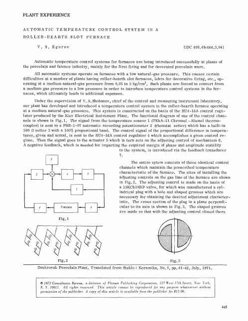
r e m a i n s a m i n i m u m p a s s a g e for gas n e c e s s a r y for s t a b l e o p e r a t i o n of the b u r n e r s without s p u t t e r i n g of the f l a m e . In addition, for s a f e t y the IM 2/120 a c t u a t o r has l i m i t s w i t c h e s which p r e v e n t c o m p l e t e c l o s i n g of the a d j u s t i n g c o n t r o l . E x p e r i m e n t a l t e s t i n g of the a u t o m a t i c c o n t r o l s y s t e m showed that it w o r k s s t a b l y ; the e r r o r does not e x c e e d 10~ The s y s t e m was t e s t e d a l s o f o r its d i s t u r b a n c e by d e f l e c t i n g the b u r n e r s in the w a r m i n g zone. In this c a s e the m a x i m u m d e v i a t i o n of the t e m p e r a t u r e f r o m the p r e s c r i b e d was 25~ the t r a n s i e n t t i m e was 6 h, and the e r r o r in the s t e a d y s t a t e was 10~ D u r i n g this t i m e the p r e s s u r e in the b u r n e r s of the c o n t r o l zone r o s e : in the u p p e r b u r n e r s f r o m 0.165 to 0.255 gauge a t m and in the l o w e r f r o m 0.065 to 0.125 gauge a i m . The f u r n a c e on which the a u t o m a t i c t e m p r a t u r e c o n t r o l s y s t e m was i n t r o d u c e d has a length of 27 m, 8 p a i r s of injection b u r n e r s , and o p e r a t e s at a m a x i m u m t e m p e r a t u r e of 960~
单片机温度控制系统毕业论文中英文资料外文翻译文献

单片机温度控制系统中英文资料外文翻译文献英文原文DescriptionThe at89s52 is a low-power, high-performance CMOS 8-bit microcomputer with 4K bytes of Flash Programmable and Erasable Read Only Memory (PEROM) and 128 bytes RAM. The device is manufactured using Atmel’s h igh density nonvolatile memory technology and is compatible with the industry standard MCS-51™ instruction set and pinout. The chip combines a versatile 8-bit CPU with Flash on a monolithic chip, the Atmelat89s52 is a powerful microcomputer which provides a highly flexible and cost effective solution to many embedded control applications.Features:• Compatible with MCS-51™ Products• 4K Bytes of In-System Reprogrammable Flash Memory• Endurance: 1,000 Write/Erase Cycles• Fully Static Operation: 0 Hz to 24 MHz• Three-Level Program Memory Lock• 128 x 8-Bit Internal RAM• 32 Programmable I/O Lines• Two 16-Bit Timer/Counters• Six Interrupt Sources• Programmable Serial Channel• Low Power Idle and Power Down ModesThe at89s52 provides the following standard features: 4K bytes of Flash, 128 bytes of RAM, 32 I/O lines, two 16-bit timer/counters, a five vectortwo-level interrupt architecture, a full duplex serial port, on-chip oscillator and clock circuitry. In addition, the at89s52 is designed with static logic for operation down to zero frequency and supports two software selectable power saving modes. The Idle Mode stops the CPU while allowing the RAM, timer/counters, serial port and interrupt system to continue functioning. The Power Down Mode saves the RAM contents but freezes the oscillator disabling all other chip functions until the next hardware reset.Pin Description:VCC Supply voltage.GND Ground.Port 0Port 0 is an 8-bit open drain bidirectional I/O port. As an output port each pin can sink eight TTL inputs. When is are written to port 0 pins, the pins can be used as high impedance inputs.Port 0 may also be configured to be the multiplexed loworderaddress/data bus during accesses to external program and data memory. In this mode P0 has internal pullups.Port 0 also receives the code bytes during Flash programming, and outputs the code bytes during program verification. External pullups are required during program verification.Port 1Port 1 is an 8-bit bidirectional I/O port with internal pullups. The Port 1 output buffers can sink/source four TTL inputs. When 1s are written to Port 1 pins they are pulled high by the internal pullups and can be used as inputs. As inputs, Port 1 pins that are externally being pulled low will source current (IIL) because of the internal pullups.Port 1 also receives the low-order address bytes during Flash programming and verification.Port 2Port 2 is an 8-bit bidirectional I/O port with internal pullups. The Port 2 output buffers can sink/source four TTL inputs. When 1s are written to Port 2 pins they are pulled high by the internal pullups and can be used as inputs. As inputs, Port 2 pins that are externally being pulled low will source current (IIL) because of the internal pullups.Port 2 emits the high-order address byte during fetches from external program memory and during accesses to external data memory that use 16-bit addresses (MOVX @ DPTR). In this application it uses strong internalpull-ups when emitting 1s. During accesses to external data memory that use 8-bit addresses (MOVX @ RI), Port 2 emits the contents of the P2 Special Function Register.Port 2 also receives the high-order address bits and some control signals during Flash programming and verification.Port 3Port 3 is an 8-bit bidirectional I/O port with internal pullups. The Port 3 output buffers can sink/source four TTL inputs. When 1s are written to Port 3 pins they are pulled high by the internal pullups and can be used as inputs. As inputs, Port 3 pins that are externally being pulled low will source current (IIL) because of the pullups.Port 3 also serves the functions of various special features of theat89s52 as listed below:Port 3 also receives some control signals for Flash programming andverification.RSTReset input. A high on this pin for two machine cycles while theoscillator is running resets the device.ALE/PROGAddress Latch Enable output pulse for latching the low byte of theaddress during accesses to external memory. This pin is also the program pulse input (PROG) during Flash programming.In normal operation ALE is emitted at a constant rate of 1/6 theoscillator frequency, and may be used for external timing or clockingpurposes. Note, however, that one ALE pulse is skipped during each access to external Data Memory.If desired, ALE operation can be disabled by setting bit 0 of SFRlocation 8EH. With the bit set, ALE is active only during a MOVX or MOVC instruction. Otherwise, the pin is weakly pulled high. Setting the ALE-disable bit has no effect if the microcontroller is in external execution mode.PSENProgram Store Enable is the read strobe to external program memory. When the at89s52 is executing code from external program memory, PSEN is activated twice each machine cycle, except that two PSENactivations are skipped during each access to external data memory.EA/VPPExternal Access Enable. EA must be strapped to GND in order to enable the device to fetch code from external program memory locations starting at 0000H up to FFFFH. Note, however, that if lock bit 1 is programmed, EA will be internally latched on reset. Port pinalternate functions P3.0rxd (serial input port) P3.1txd (serial output port) P3.2^int0 (external interrupt0) P3.3^int1 (external interrupt1) P3.4t0 (timer0 external input) P3.5t1 (timer1 external input) P3.6^WR (external data memory write strobe) P3.7 ^rd (external data memory read strobe)EA should be strapped to VCC for internal program executions.This pin also receives the 12-volt programming enable voltage(VPP) during Flash programming, for parts that require 12-volt VPP.XTAL1Input to the inverting oscillator amplifier and input to the internal clock operating circuit.XTAL2Output from the inverting oscillator amplifier.Oscillator CharacteristicsXTAL1 and XTAL2 are the input and output, respectively, of an inverting amplifier which can be configured for use as an on-chip oscillator, as shown in Figure 1. Either a quartz crystal or ceramic resonator may be used. To drive the device from an external clock source, XTAL2 should be left unconnected while XTAL1 is driven as shown in Figure 2. There are no requirements on the duty cycle of the external clock signal, since the input to the internal clocking circuitry is through a divide-by-two flip-flop, but minimum and maximum voltage high and low time specifications must be observed.Idle ModeIn idle mode, the CPU puts itself to sleep while all the onchip peripherals remain active. The mode is invoked by software. The content of the on-chip RAM and all the special functions registers remain unchanged during this mode. The idle mode can be terminated by any enabled interrupt or by a hardware reset.It should be noted that when idle is terminated by a hard ware reset, the device normally resumes program execution, from where it left off, up to two machine cycles before the internal reset algorithm takes control. On-chip hardware inhibits access to internal RAM in this event, but access to the port pins is not inhibited. To eliminate the possibility of an unexpected write to a port pin when Idle is terminated by reset, the instruction following the one that invokes Idle should not be one that writes to a port pin or to external memory.Status of External Pins During Idle and Power Down Modesmode Program memory ALE ^psen Port0 Port1Port2Port3idle internal 1 1 data data data Data Idle External 1 1 float Data data Data Power down Internal 0 0 Data Data Data Data Power down External 0 0 float data Data data Power Down ModeIn the power down mode the oscillator is stopped, and the instructionthat invokes power down is the last instruction executed. The on-chip RAMand Special Function Registers retain their values until the power down modeis terminated. The only exit from power down is a hardware reset. Resetredefines the SFRs but does not change the on-chip RAM. The reset shouldnot be activated before VCC is restored to its normal operating level andmust be held active long enough to allow the oscillator to restart andstabilize.Program Memory Lock BitsOn the chip are three lock bits which can be left unprogrammed (U) orcan be programmed (P) to obtain the additional features listed in the tablebelow:Lock Bit Protection ModesWhen lock bit 1 is programmed, the logic level at the EA pin issampled and latched during reset. If the device is powered up without a reset,the latch initializes to a random value, and holds that value until reset isactivated. It is necessary that the latched value of EA be in agreement with the current logic level at that pin in order for the device to function properly. Programming the Flash:The at89s52 is normally shipped with the on-chip Flash memory array in the erased state (that is, contents = FFH) and ready to be programmed.The programming interface accepts either a high-voltage (12-volt) or alow-voltage (VCC) program enable signal.The low voltage programming mode provides a convenient way to program the at89s52 inside the user’s system, while the high-voltage programming mode is compatible with conventional third party Flash or EPROM programmers.The at89s52 is shipped with either the high-voltage or low-voltage programming mode enabled. The respective top-side marking and device signature codes are listed in the following table.Vpp=12v Vpp=5vTop-side mark at89s52xxxxyywwat89s52xxxx-5yywwsignature (030H)=1EH(031H)=51H(032H)=FFH (030H)=1EH (031H)=51H (032H)=05HThe at89s52 code memory array is programmed byte-bybyte in either programming mode. To program any nonblank byte in the on-chip Flash Programmable and Erasable Read Only Memory, the entire memory must be erased using the Chip Erase Mode.Programming Algorithm:Before programming the at89s52, the address, data and control signals should be set up according to the Flash programming mode table and Figures 3 and 4. To program the at89s52, take the following steps.1. Input the desired memory location on the address lines.2. Input the appropriate data byte on the data lines.3. Activate the correct combination of control signals.4. Raise EA/VPP to 12V for the high-voltage programming mode.5. Pulse ALE/PROG once to program a byte in the Flash array or the lock bits. The byte-write cycle is self-timed and typically takes no more than 1.5 ms. Repeat steps 1 through 5, changing the address and data for the entire array or until the end of the object file is reached.Data Polling: The at89s52 features Data Polling to indicate the end of a write cycle. During a write cycle, an attempted read of the last byte written will result in the complement of the written datum on PO.7. Once the write cycle has been completed, true data are valid on all outputs, and the next cycle may begin. Data Polling may begin any time after a write cycle has been initiated.Ready/Busy: The progress of byte programming can also be monitored by the RDY/BSY output signal. P3.4 is pulled low after ALE goes high during programming to indicate BUSY. P3.4 is pulled high again when programming is done to indicate READY.Program Verify: If lock bits LB1 and LB2 have not been programmed, the programmed code data can be read back via the address and data lines for verification. The lock bits cannot be verified directly. Verification of the lock bits is achieved by observing that their features are enabled.Chip Erase: T he entire Flash Programmable and Erasable Read Only Memory array is erased electrically by using the proper combination of control signals and by holding ALE/PROG low for 10 ms. The code array is written with all “1”s. The chip erase operation must be executed before the code memory can be re-programmed.Reading the Signature Bytes: The signature bytes are read by the same procedure as a normal verification of locations 030H, 031H, and 032H, except that P3.6 and P3.7 must be pulled to a logic low. The values returned are as follows.(030H) = 1EH indicates manufactured by Atmel(031H) = 51H indicates 89C51(032H) = FFH indicates 12V programming(032H) = 05H indicates 5V programmingProgramming InterfaceEvery code byte in the Flash array can be written and the entire array can be erased by using the appropriate combination of control signals. The write operation cycle is selftimed and once initiated, will automatically time itself to completion.中文翻译描述at89s52是美国ATMEL公司生产的低电压,高性能CMOS8位单片机,片内含4Kbytes的快速可擦写的只读程序存储器(PEROM)和128 bytes 的随机存取数据存储器(RAM),器件采用ATMEL公司的高密度、非易失性存储技术生产,兼容标准MCS-51产品指令系统,片内置通用8位中央处理器(CPU)和flish存储单元,功能强大at89s52单片机可为您提供许多高性价比的应用场合,可灵活应用于各种控制领域。
温室环境监测和控制系统外文翻译文献

温室环境监测和控制系统外文翻译文献(文档含中英文对照即英文原文和中文翻译)New Environment Parameters Monitoring And Control System For Greenhouse Based On Master-slave DistributedAbstractAccording to the actual need of monitoring and control of greenhouse environment parameters in rural areas,a master-slave distributed measurement and control system is designed,in which PC is taken as the host. The system consists of PC ,soil moisture measurement and control module,temperature and humidity, andCO2 monitoring and control module. In the system,PC has large amount of data storage which is easy to make use of fuzzy control expert system,configuration software-KingView is used to develop software for PC,by which the development cycle is shorten and a friendly human-computer interaction is provided.Each monitoring and control module consists of STC12 series of microcontrollers,sensors,relays etc.Different modules are select based on the need if system to achieve control greenhouse in partition and block.I INTRODUCTIONTo modern indoor agriculture, the automatic measurement and control of environment parameters is the key to achieve crop yield and quality of greenhouse.In recent years,facilities agriculture develops vigorously in our country,matched with it,the monitoring and control instrument of greenhouse have also made certain development.After nearly 10 years of unremitting hard work,our research team of measurement and control system of agriculture environment parameters,designed an intelligent measurement and control system of distribution combined of greenhouse which can be popularized in the vast rural areas.This system is mainly control of temperature,humidity,CO2 concentration,soil moisture and illumination of greenhouse.OF SCM,as the data storage is small,display interface is single,amount of information is limited,but its capability price ratio is high,so it is used as a front unit of data acquisition and control;and of PC,it has a large amount of data storage,rich software,convenient human-computer interaction,and so on.If we use outdated and low-priced PC,taking the PC as the upper machine,taking the different function control modules composed of multiple microcomputers as the lower machines,then a master-slave distributed and intelligent control system bases on microcomputer is made up,by which both better monitoring and control,display and data collection or management are achieved,but also lower cost of system is get according to the actual need.II SYSTEM STRUCTURE AND PRINCIPLEThe most marked feature of the distribution combined and intelligent control system greenhouse is that of incorporating with data acquisition, control and management as a whole,module combination, simple structure,convenient human-computer interaction,and using technology of intelligent expert fuzzycontrol,which can adapt to a variety of crop management control in greenhouse.The basic structure of the system is shown in Fig.1.The structure of the distributed system is composed of two layers:the upper and lower.In the top-price PC is taken as the host to make system management and experts fuzzy operation in intelligent,and to provide a friendlyhuman-computer interface,and to realize the united monitoring and management of greenhouse; the lower is composed of a series of modules of different function,and in each module,a single chip of AT89C is adopted as the lower machine,RS485 is used to communicate PC with all AT89C,and then the collection,processing and control of the greenhouse parameters is achieved.Each function module is completely isolated in electrical,any failure on the nodule does not produce any effect on other modules.The system collects separately ways of environment information through each monitoring and control module,and sends it to host PC through the RS485 interface.And in the PC configuration control system,the acquired parameters are compared with the values of setting,then according to a variety of expert intelligent fuzzy control system of crops at different growth stages,the fuzzy control instructions on the environment temperature,humidity,CO2 concentration,soil water content and the corresponding operation instructions or alarm are given.The system is applied in rural greenhouses in ually at 1/4 near East and West end in a greenhouse,and at the height of 1.5m from the ground in the middle in the northern half (near the wet curtain) and the southern half (near the fan ),a module of air temperature and humidity ,CO2 concentration and a module of soil moisture content are set;a module of soil moisture content will be added in the middle of the greenhouse according to the actual condition;at the height of 1.5m in the main entrance,a water tank is set,of which the solenoid of drip tube should be set based on the need and controlled by module of soil moisture content;and the PC is placed in the main entrance to the greenhouse.III HARDWARE DESIGNA.The CP and communication systemIn the distributed system of data acquisition and control,as the micro control unit is limited in data storage and slow in calculating of complex functions,so PC is used and the master-slave module is adopted in the system,that is a system of,taking PC as the host and taking the SCM systems located in the scene as slave.In this distributed system,communication is the key to it.Generally,the serial port of PC is standard RS232,of which transmission distance is shorter.But in agriculture control system.its communication distance is of tens of meters or several kilometers, so RS232/RS485 converter is used to achieve communication between the PC and SCM.To reduce investment,both considering the user convenience and friendly human-computer interaction,low-price PC of above 486 and below PIV is adopted;and considering the operation of configuration software,it is required that memory is 64M or above and hard disk is 10Gb or above.B. The control modules of temperature and humidity,illuminance and CO2 concentrationEach control unit consists of SCM,sensors,signal processing circuit,RS485 interface and output circuit.The hardware structure of module of temperature and humidity,CO2 concentration is shown in Fig.2.CO2concentration is measured by sensor based on NDIR technology,measurement is of 0~2×10³mol.Through the sensor,control system,by software of digital filter,linear interpolation and temperature compensation,the CO2 concentration is output as digital adhered to UART protocol,and then is input directly to the SCM.The new intelligent sensor of SHT11 based on CMOSens technology is chosen in the measurement of temperature and humidity.In SHT11,the temperature and humidity sensors,signal amplification,A/D,I2C bus are all integrated in a chip;it has full-scale calibration,second-line digital output,and humidity measuring range of 0~100% RH,temperature measurement range of -40℃~+123.8℃,humidity measurement accuracy of ±3.0% RH,temperature measurement accuracy of ±0.4℃,the response time of <4s.The illuminance sensor of JY1-TBQ-6 of silicon photovoltaic detection is used Light measuring.Its measurement range is 0~200,000 Lux;spectral range is 400~700(nm) visible light;measurement error is less than 2%; output is 4~20mA or 0~20mV;output signal can be directly send to the A/D of the SCM after being amplified to 0~4V.Modules accept the instructions form the the Upper,and output via the output circuit .The output circuit consists of optical isolation,the signal driver and the output relays.C. The measurement and control modules of soil moistureWater is a polar medium, the dielectric constant of the soil containing water is mainly determined by the water,when water content is different,the wave impedance is different.The soil moisture is measured by standing wave radio method in thissystem.Based on the theory of Engineering Electromagnetic Field,for lossy medium,the electromagnetic wave impedance as follows:Z0=√μ/ε(1+jλ/(ωε))Where μ is medium permeability,and μ of soil is μ≈μ0 is the vacuum permeability;ε is medium dielectric constant;λ is medium conductivity;ω is electromagnetic wave frequency.In the very low audio(<2000Hz),the loss tangent of dry soil dielectric is λ/ωε≈0.07,if you choose the frequency of the si gnal source at above 20MHz.then,ε≈ε∞,the imaginary part of the soil wave impedance is neglect,only the real part,which amounts to a pure resistance.Soil moisture sensor consists of 100MHz signal source,a coaxial transmission line and a 4-pin stainless probe.The electromagnetic waves of signal transmit to the probe along the lines.As the probe impedance and line impedance are different,the superimposition of incident waves and reflected waves forms a standing waves.Taking the coaxial transmission line as a lossless uniform line,wave impedance is Z0,Z l is the load impedance.Then the reflected coefficient of voltage wave at the probe is:Γ=(Z L-Z0)/(Z L+Z0)Choosing the length of transmission line is l=λ/4,the maximum and minimum of both ends of the line are U max and U min,Then the standing wave radio in the line can be expressed as:S=U max /U min =(1-|Γ|)/(1+|Γ|)In the way,the soil moisture radio can be measured by measuring the standing wave rate of transmission line.As shown in Fig.3.,soil moisture module consists of sensors and controllers,the sensors are subordinated to controllers,controllers can be omitted without the need of irrigation in greenhouse.To simplify the control,irrigation technology of node-type in partition is adopted in the control soil moisture in this system.To a certain extent,the parameters of upper and lower the ground can be decoupled by adopting this technology.IV CONTROL SYSTEM PROGRAMMINGThe software of PC is developed by KingView 6.51 of Beijing-controlled Asia.This configuration software has high reliability,shorter development cycle,perfect capability of graphical interface generation,and friendly human-computer interaction;and can create dynamic images and charts in accordance with the layout of equipment in the scene;can visually display the changes of parameters,control status,and can give an alarm when over-limited;and can achieve fuzzy control of greenhouse parameters by using the history curve of environment parameters stored in the specific database and adopting the agricultural expert system.The software of SCM of the slave is developed by Keil C51 to achieve real-time collecting,processing,uploading of the parameters and accept the fuzzy control instructions from the host computer and complete local control of the device.A.Program design of the control moduleThe software of the sub-slave machine of soil moisture module,that include the main function,subroutines of data acquisition and processing,interrupt handling andcommunicating etc,read the value of standing wave voltage through the parallel data port and obtained the value of soil moisture content by function calculating.The software of the slave machine of monitoring and control of soil moisture mainly complete data communication with the sub-slave machine,uploading measurement data and current control state to the host computer,accepting the fuzzy control instructions from the host computer and output the implementation instructions.The software of the slave machine of temperature and humidity,and CO2 mainly complete reading data of CO2 concentrations and temperature and humidity through the I2C concentration,uploading measurement data and current control state to the host computer,accepting the fuzzy control instructions from the host computer and output the implementation instructions.The structure of the main program and interrupt subroutine of temperature and humidity module are shown in Fig.4.The serial interrupt mode 3 is adopted by all slaves to communicate with the host,transmit the digital collecting and receive instructions.B. Program design of PC and fuzzy control system1)The communication settings of KingView 6.51:In order to ensure the correctness of communication,the upper and lower must follow the same communication protocol,set the communication ually in communication,master-slave mode is adopted in style and responder is adopted in the process.That is ,the master sent a command to the slave first,then et slave give an answer after receiving the command,thus once communication is completed.In KingView ,a scheduled polling method is adopted to do reading and writing between the lower machine by PC.In the project browser of KingView,first,click device →COM1;in the wizard of device configuration,select intelligent modules→SCM→current SCM of HEX→serial port,and then ser parameters for the host computer’s communication.2)The connection of KingView 6.51 and database:Database is the core of the software,that not only contains the definition of variables,real-time parameters and the historical parameters,but also is needed by parameters alarming,fuzzy calculating,reporting ,and displaying.Access2003 desktop database is used as records database of the system,and by using SQL,it is operated by KingView via ODBC.The procedure is :to create data variables in KingView to create a body of records toestablish a data source of ODBC to create query screens and make the screen connection.To connected with Microsoft Access2003,the functions of SQLConnect(),SQLSelect(),SQLLast(),SQLNext(),SQLFist(),SQLPrew(),SQLInsrt() ,and so on,should be implemented in the command language,and then real-time storage and inquiry of data are completed.3)Software design of PC :For the control system of greenhouse,data storage capacity of the PC is unlimited,so if the existing mature software modules are include into the system,it both be relaxed and can improve the system reliability.The software of software consists of control module and management module.V CONCLUSIONAccording to the economic bearing capacity of farmer in Qinhuangdao ,with the existing technology of monitoring and control of environment parameters of greenhouse,a master-slave distributed automatic control system of greenhouse environment in which PC is taken as the host computer is developed.The system has following characteristics:1)With the large amount of data storage of PC,fuzzy control expert system is easy of data storage,modification and system upgrading.2)By using KingView to develop software of PC,the system reliability is improved,and the development cycle is shorten,and a friendly human-computer interface is get.3)A distributed and modular structure is used in the system,it makes the system maintenance easier and adapts to production needs more. The monitoring and control modules of the slave are connected to the host through the RS485 bus based on needs,then the control of greenhouse in partition or block can be achieved.基于新的温室环境参数监测和控制系统根据实际在农村地区的温室环境参数的监测和控制,主从分布式测量和控制系统的设计需要,以其中一台计算机作为主机,该系统由PC、土壤水分测量和控制模块,温度、湿度、CO2监测和控制模块组成。
单片机-温度控制系统-外文翻译-外文文献-英文文献-中英翻译

Design of the Temperature Control System Based on AT89C51ABSTRACTThe principle and functions of the temperature control system based on micro controller AT89C51 are studied, and the temperature measurement unit consists of the 1-Wire bus digital temperature sensor DS18B20. The system can be expected to detect the preset temperature, display time and save monitoring data. An alarm will be given by system if the temperature exceeds the upper and lower limit value of the temperature which can be set discretionarily and then automatic control is achieved, thus the temperature is achieved monitoring intelligently within a certain range. Basing on principle of the system, it is easy to make a variety of other non-linear control systems so long as the software design is reasonably changed. The system has been proved to be accurate, reliable and satisfied through field practice.KEYWORDS: AT89C51; micro controller; DS18B20; temperature1 INTRODUCTIONTemperature is a very important parameter in human life. In the modern society, temperature control (TC) is not only used in industrial production, but also widely used in other fields. With the improvement of the life quality, we can find the TC appliance in hotels, factories and home as well. And the trend that TC will better serve the whole society, so it is of great significance to measure and control the temperature. Based on the AT89C51 and temperature sensor DS18B20, this system controls the condition temperature intelligently. The temperature can be set discretionarily within a certain range. The system can show the time on LCD, and save monitoring data; and automatically control the temperature when the condition temperature exceeds the upper and lower limit value. By doing so it is to keep the temperature unchanged. The system is of high anti-jamming, high control precision and flexible design; it also fits the rugged environment. It is mainly used in people's life to improve the quality of the work and life. It is also versatile, so that it can beconvenient to extend the use of the system. So the design is of profound importance. The general design, hardware design and software design of the system are covered.1.1 IntroductionThe 8-bit AT89C51 CHMOS microcontrollers are designed to handle high-speed calculations and fast input/output operations. MCS 51 microcontrollers are typically used for high-speed event control systems. Commercial applications include modems, motor-control systems, printers, photocopiers, air conditioner control systems, disk drives, and medical instruments. The automotive industry use MCS 51 microcontrollers in engine-control systems, airbags, suspension systems, and antilock braking systems (ABS). The AT89C51 is especially well suited to applications that benefit from its processing speed and enhanced on-chip peripheral functions set, such as automotive power-train control, vehicle dynamic suspension, antilock braking, and stability control applications. Because of these critical applications, the market requires a reliable cost-effective controller with a low interrupt latency response, ability to service the high number of time and event driven integrated peripherals needed in real time applications, and a CPU with above average processing power in a single package. The financial and legal risk of having devices that operate unpredictably is very high. Once in the market, particularly in mission critical applications such as an autopilot or anti-lock braking system, mistakes are financially prohibitive. Redesign costs can run as high as a $500K, much more if the fix means 2 back annotating it across a product family that share the same core and/or peripheral design flaw. In addition, field replacements of components is extremely expensive, as the devices are typically sealed in modules with a total value several times that of the component. To mitigate these problems, it is essential that comprehensive testing of the controllers be carried out at both the component level and system level under worst case environmental and voltage conditions. This complete and thorough validation necessitates not only a well-defined process but also a proper environment and tools to facilitate and execute the mission successfully. Intel Chandler Platform Engineering group provides post silicon system validation (SV)of various micro-controllers and processors. The system validation process can be broken into three major parts. The type of the device and its application requirements determine which types of testing are performed on the device.1.2 The AT89C51 provides the following standard features4Kbytes of Flash, 128 bytes of RAM, 32 I/O lines, two 16-bittimer/counters, a five vector two-level interrupt architecture, a full duple ser-ial port, on-chip oscillator and clock circuitry. In addition, the AT89C51 is designed with static logic for operation down to zero frequency and supports two software selectable power saving modes. The Idle Mode stops the CPU while allowing the RAM, timer/counters, serial port and interrupt sys -tem to continue functioning. The Power-down Mode saves the RAM contents but freezes the oscil–lator disabling all other chip functions until the next hardware reset.1.3Pin DescriptionVCC Supply voltage.GND Ground.Port 0:Port 0 is an 8-bit open-drain bi-directional I/O port. As an output port, each pin can sink eight TTL inputs. When 1s are written to port 0 pins, the pins can be used as high impedance inputs. Port 0 may also be configured to be the multiplexed low order address/data bus during accesses to external program and data memory. In this mode P0 has internal pull ups. Port 0 also receives the code bytes during Flash programming, and outputs the code bytes during program verification. External pull ups are required during program verification.Port 1:Port 1 is an 8-bit bi-directional I/O port with internal pull ups. The Port 1 output buffers can sink/so -urce four TTL inputs. When 1s are written to Port 1 pins they are pulled high by the internal pull ups and can be used as inputs. As inputs, Port 1 pins that are externally being pulled low will source current (IIL) because of the internal pullups. Port 1 also receives the low-order address bytes during Flash programming and verification.Port 2:Port 2 is an 8-bit bi-directional I/O port with internal pullups. The Port 2 output buffers can sink/source four TTL inputs. When 1s are written to Port 2 pins they are pulled high by the internal pull ups and can be used as inputs. As inputs, Port 2 pins that are externally being pulled low will source current (IIL) because of the internal pull ups. Port 2 emits the high-order address byte during fetches from external program memory and during accesses to Port 2 pins that are externally being pulled low will source current (IIL) because of the internal pull ups. Port 2 emits the high-order address byte during fetches from external program memory and during accesses to external data memory that use 16-bit addresses (MOVX@DPTR). In this application, it uses strong internal pull-ups when emitting 1s. During accesses to external data memory that use 8-bit addresses (MOVX @ RI), Port 2 emits the contents of the P2 Special Function Register. Port 2 also receives the high-order address bits and some control signals durin Flash programming and verification.Port 3:Port 3 is an 8-bit bi-directional I/O port with internal pull ups. The Port 3 output buffers can sink/sou -rce four TTL inputs. When 1s are written to Port 3 pins they are pulled high by the internal pull ups and can be used as inputs. As inputs, Port 3 pins that are externally being pulled low will source current (IIL) because of the pull ups.Port 3 also serves the functions of various special features of the AT89C51 as listed below:RST:Reset input. A high on this pin for two machine cycles while the oscillator is running resets the device.ALE/PROG:Address Latch Enable output pulse for latching the low byte of the address during accesses to external memory. This pin is also the program pulse input (PROG) during Flash programming. In normal operation ALE is emitted at a constant rate of 1/6 the oscillator frequency, and may be used for external timing or clocking purposes. Note, however, that one ALE pulse is skipped duri-ng each access to external Data Memory. If desired, ALE operation can be disabled by setting bit 0 of SFR location 8EH. With the bit set, ALE is active only during a MOVX or MOVC instruction. Otherwise, the pin is weakly pulled high. Setting the ALE-disable bit has no effect if the microcontroller is in external execution mode.PSEN:Program Store Enable is the read strobe to external programmemory. When theAT89C51 is executing code from external program memory, PSEN is activated twice each machine cycle, except that two PSEN activations are skipped during each access to external data memory.EA/VPP:External Access Enable. EA must be strapped to GND in order to enable the device to fetch code from external program memory locations starting at 0000H up to FFFFH. Note, however, that if lock bit 1 is programmed, EA will be internally latched on reset. EA should be strapped to VCC for internal program executions. This pin alsreceives the 12-volt programming enable voltage (VPP) during Flash programming, for parts that require 12-volt VPP.XTAL1:Input to the inverting oscillator amplifier and input to the internal clock operating circuit.XTAL2 :Output from the inverting oscillator amplifier. Oscillator CharacteristicsXTAL1 and XTAL2 are the input and output, respectively, of an inverting amplifier which can be configured for use as an on-chip oscillator, as shown in Figure 1. Either a quartz crystal or ceramic resonator may be used. To drive the device from an external clock source, XTAL2 should be left unconnected while XTAL1 is driven as shown in Figure 2.There are no requirements on the duty cycle of the external clock signal, since the input to the internal clocking circuitry is through a divide-by-two flip-flop, but minimum and maximum voltage high and low time specifications must be observed. Idle Mode In idle mode, the CPU puts itself to sleep while all the on chip peripherals remain active. The mode is invoked by software. The content of the on-chip RAM and all the special functions registers remain unchanged during this mode. The idle mode can be terminated by any enabled interrupt or by a hardware reset. It should be noted that when idle is terminated by a hard ware reset, the device normally resumes program execution, from where it left off, up to two machine cycles before the internal reset algorithm takes control. On-chip hardware inhibits access to internal RAM in this event, but access to the port pins is not inhibited. To eliminate the possibility of an unexpected write to a port pin when Idle is terminated by reset, the instruction following the one that invokes Idle should not be one that writes to a port pin or to external memory.Power-down ModeIn the power-down mode, the oscillator is stopped, and the instruction that invokes power-down is the last instruction executed. The on-chip RAM and Special Function Registers retain their values until the power-down mode is terminated. The only exit from power-down is a hardware reset. Reset redefines the SFRS but does not change the on-chip RAM. The reset should not be activated before VCC is restored to its normal operating level and must be held active long enough to allow the oscillator to restart and stabilize. The AT89C51 code memory array is programmed byte-by byte in either programming mode. To program any nonblank byte in the on-chip Flash Memory, the entire memory must be erased using the Chip Erase Mode.2 Programming AlgorithmBefore programming the AT89C51, the address, data and control signals should be set up according to the Flash programming mode table and Figure 3 and Figure 4. To program the AT89C51, take the following steps.1. Input the desired memory location on the address lines.2. Input the appropriate data byte on the data lines. 3. Activate the correct combination of control signals. 4. Raise EA/VPP to 12V for the high-voltage programming mode.5. Pulse ALE/PROG once to program a byte in the Flash array or the lock bits. The byte-write cycle is self-timed and typically takes no more than 1.5 ms. Repeat steps 1 through 5, changing the address and data for the entire array or until the end of the object file is reached. Data Polling: The AT89C51 features Data Polling to indicate the end of a write cycle. During a write cycle, an attempted read of the last byte written will result in the complement of the written datum on PO.7. Once the write cycle has been completed, true data are valid on all outputs, and the next cycle may begin. Data Polling may begin any time after a write cycle has been initiated.2.1Ready/Busy:The progress of byte programming can also be monitored by the RDY/BSY output signal. P3.4 is pulled low after ALE goes high during programming to indicate BUSY. P3.4 is pulled high again when programming is done toindicate READY.Program Verify:If lock bits LB1 and LB2 have not been programmed, the programmed code data can be read back via the address and data lines for verification. The lock bits cannot be verified directly. Verification of the lock bits is achieved by observing that their features are enabled.2.2 Chip Erase:The entire Flash array is erased electrically by using the proper combination of control signals and by holding ALE/PROG low for 10 ms. The code array is written with all “1”s. The chip erase operation must be executed before the code memory can be re-programmed.2.3 Reading the Signature Bytes:The signature bytes are read by the same procedure as a normal verification of locations 030H, 031H, and 032H, except that P3.6 and P3.7 must be pulled to a logic low. The values returned areas follows.(030H) = 1EH indicates manufactured by Atmel(031H) = 51H indicates 89C51(032H) = FFH indicates 12V programming(032H) = 05H indicates 5V programming2.4 Programming InterfaceEvery code byte in the Flash array can be written and the entire array can be erased by using the appropriate combination of control signals. The write operation cycle is self timed and once initiated, will automatically time itself to completion. A microcomputer interface converts information between two forms. Outside the microcomputer the information handled by an electronic system exists as a physical signal, but within the program, it is represented numerically. The function of any interface can be broken down into a number of operations which modify the data in some way, so that the process of conversion between the external and internal forms is carried out in a number of steps. An analog-to-digital converter(ADC) is used to convert a continuously variable signal to a corresponding digital form which can take any one of a fixed number of possible binary values. If the output of thetransducer does not vary continuously, no ADC is necessary. In this case the signal conditioning section must convert the incoming signal to a form which can be connected directly to the next part of the interface, the input/output section of the microcomputer itself. Output interfaces take a similar form, the obvious difference being that here the flow of information is in the opposite direction; it is passed from the program to the outside world. In this case the program may call an output subroutine which supervises the operation of the interface and performs the scaling numbers which may be needed for digital-to-analog converter(DAC). This subroutine passes information in turn to an output device which produces a corresponding electrical signal, which could be converted into analog form using a DAC. Finally the signal is conditioned(usually amplified) to a form suitable for operating an actuator. The signals used within microcomputer circuits are almost always too small to be connected directly to the outside world” and some kind of interface must be used to translate them to a more appropriate form. The design of section of interface circuits is one of the most important tasks facing the engineer wishing to apply microcomputers. We have seen that in microcomputers information is represented as discrete patterns of bits; this digital form is most useful when the microcomputer is to be connected to equipment which can only be switched on or off, where each bit might represent the state of a switch or actuator. To solve real-world problems, a microcontroller must have more than just a CPU, a program, and a data memory. In addition, it must contain hardware allowing the CPU to access information from the outside world. Once the CPU gathers information and processes the data, it must also be able to effect change on some portion of the outside world. These hardware devices, called peripherals, are the CPU’s window to the outside.The most basic form of peripheral available on microcontrollers is the general purpose I70 port. Each of the I/O pins can be used as either an input or an output. The function of each pin is determined by setting or clearing corresponding bits in a corresponding data direction register during the initialization stage of a program. Each output pin may be driven to either a logic one or a logic zero by using CPU instructions to pinmay be viewed (or read.) by the CPU using program instructions. Some type of serial unit is included on microcontrollers to allow the CPU to communicate bit-serially with external devices. Using a bit serial format instead of bit-parallel format requires fewer I/O pins to perform the communication function, which makes it less expensive, but slower. Serial transmissions are performed either synchronously or asynchronously.3 SYSTEM GENERAL DESIGNThe hardware block diagram of the TC is shown in Fig. 1. The system hardware includes the micro controller, temperature detection circuit, keyboard control circuit, clock circuit, Display, alarm, drive circuit and external RAM. Based on the AT89C51, the DS18B20 will transfer the temperature signal detected to digital signal. And the signal is sent to the micro controller for processing. At last the temperature value is showed on the LCD 12232F. These steps are used to achieve the temperature detection. Using the keyboard interface chip HD7279 to set the temperature value, using the micro controller to keep a certain temperature, and using the LCD to show the preset value for controlling the temperature. In addition, the clock chip DS1302 is used to show time and the external RAM 6264 is used to save the monitoring data. An alarm will be given by buzzer in time if the temperature exceeds the upper and lower limit value of the temperature.3.1 HARDWARE DESIGNA. Micro controllerThe AT89C51 is a low-power, high-performance CMOS 8-bit micro controller with 4K bytes of in-system programmable Flash memory. The device is manufactured using At mel’s high-density nonvolatile memory technology and is compatible with the industry-standard 80C51 instruction set and pin out. The on-chip Flash allows the program memory to be reprogrammed in-system or by a conventional nonvolatile memory programmer. By combining a versatile 8-bit CPU with in-system programmable Flash on a monolithic chip, the At mel AT89C51 is a powerful micro controller which provides a highly-flexible and cost-effective solution to many embedded control applications. Minimum system of the micro controller is shown inFig. 2. In order to save monitoring data, the 6264 is used as an external RAM. It is a static RAM chip, low-power with 8K bytes memory.B. Temperature Detection CircuitThe temperature sensor is the key part in the system. The Dallas DS18B20 is used, which supports the 1-Wire bus interface, and the ON-BOARD Patented is used internally. All the sensor parts and the converting circuit are integrated in integrated circuit like a transistor [1]. Its measure range is -55℃~125 ℃, and the precision between -10℃~85℃is ±0.5℃[2 ,3]. The temperature collected by the DS18B20 is transmitted in the 1-Wire bus way, and this highly raises the system anti-jamming and makes it fit in situ temperature measurement of the rugged environment [4]. There are two power supply ways for the DS18B20. The first is external power supply: the first pin of the DS18B20 is connected to the ground; the second pin serves as signal wire and the third is connected to the power. The second way is parasite power supply [5]. As the parasite power supply will lead to the complexity of the hardware circuit, the difficulty of the software control and the performance degradation of the chip, etc. But the DS18B20(s) can be connected to the I/O port of the micro controller in the external power supply way and it is more popular. Therefore the external power supply is used and the second pin is connected to the pin P1.3 of the AT89S51. Actually, if there are multipoint to be detected, the DS18B20(s) can be connected to the 1-Wire bus. But when the number is over 8, there is a concern to the driving and the more complex software design as well as the length of the 1-Wire bus. Normally it is no more than 50m. To achieve distant control, the system can be designed in to a wireless one to breakthe length limit of the 1-Wire bus [6].C. LCD CircuitThe LCD 12232F is used, which can be used to show characters, temperature value and time, and supply a friendly display interface. The 12232F is a LCD with 8192 128×32 pixels Chinese character database and 128 16×8 pixels ASCII character set graphics. It mainly consists of row drive/column drive and 128×32 full lattice LCD with the function of displaying graphics as well as 7.5×2 Chinese characters. It is in aparallel or serial mode to connect to external CPU [7]. In order to economize the hardware resource, the 12232F should be connected to the AT89S51 in serial mode with only 4 output ports used. The LCD grayscale can be changed by adjusting the variable resistor connected the pin Vlcd of the LCD. CLK is used to transmit serial communication clock. SID is used to transmit serial data. CS is used to enable control the LCD. L+ is used to control the LCD backlight power.D. Clock CircuitThe Dallas DS18B20 is used, which is a high performance, low-power and real-time clock chip with RAM. The DS18B20 serves in the system with calendar clock and is used to monitor the time. The time data is read and processed by the AT89C51 and then displayed by the LCD. Also the time can be adjusted by the keyboard. The DS18B20 crystal oscillator is set at 32768Hz, and the recommended compensation capacitance is 6pF. The oscillator frequency is lower, so it might be possible not to connect the capacitor, and this would not make a big difference to the time precision. The backup power supply can be connected to a 3.6V rechargeable battery.E. Keyboard Control CircuitThe keyboard interface in the system is driven by the HD7279A which has a +5V single power supply and which is connected to the keyboard and display without using any active-device. According to the basic requirements and functions of the system, only 6 buttons are needed. The system's functions are set by the AT89C51 receiving the entered data. In order to save the external resistor, the 1×6 keyboard is used, and the keyboard codes are defined as: 07H, 0FH, 17H, 1FH, 27H, 2FH. The order can be read out by reading the code instruction. HD7279A is connected to the AT89S51 in serial mode and only 4 ports are need. As shown in Fig. 6, DIG0~DIG5 and DP are respectively the column lines and row line ports of the six keys which achieve keyboard monitoring, decoding and key codes identification.F. Alarm CircuitIn order to simplify the circuit and convenient debugging, a 5V automatic buzzer is used in the alarm circuit [8]. And this make the software programming simplified. As shown in Fig. 7, it is controlled bythe PNP transistor 9012 whose base is connected to the pin P2.5 of the AT89C51. When the temperature exceeds the upper and lower limit value, the P2.5 output low level which makes the transistor be on and then an alarm is given by the buzzer.G. Drive CircuitA step motor is used as the drive device to control the temperature. The four-phase and eight-beat pulse distribution mode is used to drive motor and the simple delay program is used to handle the time interval between the pulses to obtain different rotational speed. There are two output states for the step motor. One: when the temperature is over the upper value, the motor rotates reversely (to low the temperature), while when lower than the lower limit value, the motor rotates normally (to raise the temperature); besides not equals the preset value. Two: when the temperature is at somewhere between the two ends and equals the preset value, the motor stops. These steps are used to achieve the temperature control. In addition, the motor speed can also be adjusted by relative buttons. As shown in Fig. 8, the code data is input through ports A11~A8 (be P2.3~P2.0) of the AT89C51 and inverted output by the inverter 74LS04. Finally it is amplified by the power amplifier 2803A to power the motor.3.2 SOFTWARE DESIGNAccording to the general design requirement and hardware circuit principle of the system, as well as the improvement of the program readability, transferability and the convenient debugging, the software design is modularized. The system flow mainly includes the following 8 steps: POST (Power-on self-test), system initiation, temperature detection, alarm handling, temperature control, clock chip DS18B20 operation, LCD and keyboard operation. The main program flow is shown in Fig. 9. Give a little analysis to the above 8 tasks, it is easy to find out that the last five tasks require the real time operation. But to the temperature detection it can be achieved with timer0 timing 1 second, that is to say temperature detection occurs per second. The system initiation includes global variable definition, RAM initiation, special function register initiation and peripheral equipment initiation. Global variable definition mainly finishes the interface definition of external interfacechip connected to the AT89C51, and special definition of some memory units. RAM initiation mainly refers to RAM processing. For example when the system is electrified the time code will be stored in the internal unit address or the scintillation flag will be cleared. The special function register initiation includes loading the initial value of timer and opening the interrupt. For example, when the system is electrified the timer is initialized. The peripheral equipment initiation refers to set the initial value of peripheral equipment. For example, when the system is electrified, the LCD should be initialized, the start-up display should be called, the temperature conversion command should be issued firstly and the clock chip DS18B20 should also be initialized. The alarm handling is mainly the lowering and the raising of temperature to make the temperature remain with the preset range. When the temperature is between the upper and the lower limit value, it goes to temperature control handling, that is to say the temperature need to be raised or lowered according to the preset value. By doing so make the condition temperature equal to the preset value and hence to reach the temperature target.4 CONCLUSIONThe temperature control system has the advantages of friendly human-computer interaction interface, simple hardware, low cost, high temperature control precision (error in the range of ±1 ℃), convenience and versatility, etc. It can be widely used in the occasions with -55℃to 125℃range, and there is a certain practical value.。
单片机温度控制系统论文中英文资料对照外文翻译文献

单片机温度控制系统论文中英文资料对照外文翻译文献原文题目:Single-chip microcomputer temperature control system DescriptionThe at89s52 is a low-power, high-performance CMOS 8-bit microcomputer with 4K bytes of Flash Programmable and Erasable Read Only Memory (PEROM) and 128 bytes RAM. The device is manufactured using Atmel’s high density nonvolatile memory technology and is compatible with the industry standard MCS-51™ instruction set and pinout. The chip combines a versatile 8-bit CPU with Flash on a monolithic chip, the Atmel at89s52 is a powerful microcomputer which provides a highly flexible and cost effective solution to many embedded control applications.Features:• Compatible with MCS-51™ Products• 4K Bytes of In-System Reprogrammable Flash Memory• Endurance: 1,000 Write/Erase Cycles• Fully Static Operation: 0 Hz to 24 MHz• Three-Level Program Memory Lock• 128 x 8-Bit Internal RAM• 32 Programmable I/O Lines• Two 16-Bit Timer/Counters• Six Interrupt Sources• Programmable Serial Channel• Low Power Idle and Po wer Down ModesThe at89s52 provides the following standard features: 4K bytes of Flash, 128 bytes of RAM, 32 I/O lines, two 16-bit timer/counters, a five vector two-level interrupt architecture, a full duplex serial port, on-chip oscillator and clock circuitry. In addition, the at89s52 is designed with static logic for operation down to zero frequency and supports two software selectable power saving modes. The Idle Mode stops the CPU while allowing the RAM,timer/counters, serial port and interrupt system to continue functioning. The Power Down Mode saves the RAM contents but freezes the oscillator disabling all other chip functions until the next hardware reset.Pin Description:VCC Supply voltage.GND Ground.Port 0Port 0 is an 8-bit open drain bidirectional I/O port. As an output port each pin can sink eight TTL inputs. When is are written to port 0 pins, the pins can be used as high impedance inputs.Port 0 may also be configured to be the multiplexed loworder address/data bus during accesses to external program and data memory. In this mode P0 has internal pullups.Port 0 also receives the code bytes during Flash programming, and outputs the code bytes during program verification. External pullups are required during program verification.Port 1Port 1 is an 8-bit bidirectional I/O port with internal pullups. The Port 1 output buffers can sink/source four TTL inputs. When 1s are written to Port 1 pins they are pulled high by the internal pullups and can be used as inputs. As inputs, Port 1 pins that are externally being pulled low will source current (IIL) because of the internal pullups.Port 1 also receives the low-order address bytes during Flash programming and verification.Port 2Port 2 is an 8-bit bidirectional I/O port with internal pullups. The Port 2 output buffers can sink/source four TTL inputs. When 1s are written to Port 2 pins they are pulled high by the internal pullups and can be used as inputs. As inputs, Port 2 pins that are externally being pulled low will source current (IIL) because of the internal pullups.Port 2 emits the high-order address byte during fetches from external program memory and during accesses to external data memory that use 16-bit addresses (MOVX @ DPTR). In this application it uses strong internal pull-ups when emitting 1s. During accesses to external data memory that use 8-bit addresses (MOVX @ RI), Port 2 emits the contents of the P2 Special Function Register.Port 2 also receives the high-order address bits and some control signals during Flash programming and verification.Port 3Port 3 is an 8-bit bidirectional I/O port with internal pullups. The Port 3 output buffers can sink/source four TTL inputs. When 1s are written to Port 3 pins they are pulled high by the internal pullups and can be used as inputs. As inputs, Port 3 pins that are externally being pulled low will source current (IIL) because of the pullups.Port 3 also serves the functions of various special features of the at89s52 as listed below:Port pin alternate functionsP3.0 rxd (serial input port)P3.1 txd (serial output port)P3.2 ^int0 (external interrupt0)Port 3 also receivessome control signals forFlash programming andverification. RSTReset input. A high on this pin for two machine cycles while the oscillator is runningresets the device.ALE/PROGAddress Latch Enable output pulse for latching the low byte of the address duringaccesses to external memory. This pin is also the program pulse input (PROG) during Flash programming.In normal operation ALE is emitted at a constant rate of 1/6 the oscillator frequency, and may be used for external timing or clocking purposes. Note, however, that one ALE pulse is skipped during each access to external Data Memory.If desired, ALE operation can be disabled by setting bit 0 of SFR location 8EH. With the bit set, ALE is active only during a MOVX or MOVC instruction. Otherwise, the pin is weakly pulled high. Setting the ALE-disable bit has no effect if the microcontroller is in external execution mode.PSENProgram Store Enable is the read strobe to external program memory.When the at89s52 is executing code from external program memory, PSEN is activated twice each machine cycle, except that two PSEN activations are skipped during each access to external data memory.EA/VPPExternal Access Enable. EA must be strapped to GND in order to enable the device to fetch code from external program memory locations starting at 0000H up to FFFFH. Note, however, that if lock bit 1 is programmed, EA will be internally latched on reset.EA should be strapped to VCC for internal program executions.This pin also receives the 12-volt programming enable voltage(VPP) during Flashprogramming, for parts that require 12-volt VPP.XTAL1Input to the inverting oscillator amplifier and input to the internal clock operating circuit. XTAL2Output from the inverting oscillator amplifier.Oscillator CharacteristicsXTAL1 and XTAL2 are the input and output, respectively, of an inverting amplifierwhich can be configured for use as an on-chip oscillator, as shown in Figure 1. Either a quartz crystal or ceramic resonator may be used. To drive the device from an external clock source, XTAL2 should be left unconnected while XTAL1 is driven as shown in Figure 2. There are no requirements on the duty cycle of the external clock signal, since the input to the internal clocking circuitry is through a divide-by-two flip-flop, but minimum and maximum voltage high and low time specifications must be observed. P3.3 ^int1 (external interrupt1) P3.4 t0 (timer0 external input) P3.5 t1 (timer1 external input) P3.6 ^WR (external data memory write strobe) P3.7^rd (external data memory read strobe)Idle ModeIn idle mode, the CPU puts itself to sleep while all the onchip peripherals remain active. The mode is invoked by software. The content of the on-chip RAM and all the special functions registers remain unchanged during this mode. The idle mode can be terminated by any enabled interrupt or by a hardware reset.It should be noted that when idle is terminated by a hard ware reset, the device normally resumes program execution, from where it left off, up to two machine cycles before the internal reset algorithm takes control. On-chip hardware inhibits access to internal RAM in this event, but access to the port pins is not inhibited. To eliminate the possibility of an unexpected write to a port pin when Idle is terminated by reset, the instruction following the one that invokes Idle should not be one that writes to a port pin or to external memory.Status of External Pins During Idle and Power Down Modesmode Program memory ALE ^psen Port0 Port1Port2Port3idle internal 1 1 data data data DataIdle External 1 1 float Data data Data Power down Internal 0 0 Data Data Data Data Power down External 0 0 float data Data data Power Down ModeIn the power down mode the oscillator is stopped, and the instruction that invokes power down is the last instruction executed. The on-chip RAM and Special Function Registers retain their values until the power down mode is terminated. The only exit from power down is a hardware reset. Reset redefines the SFRs but does not change the on-chip RAM. The reset should not be activated before VCC is restored to its normal operating level and must be held active long enough to allow the oscillator to restart and stabilize.Program Memory Lock BitsOn the chip are three lock bits which can be left unprogrammed (U) or can be programmed (P) to obtain the additional features listed in the table below:Lock Bit Protection ModesWhen lock bit 1 is programmed, the logic level at the EA pin is sampled and latchedduring reset. If the device is powered up without a reset, the latch initializes to a random value, and holds that value until reset is activated. It is necessary that the latched value of EA be in agreement with the current logic level at that pin in order for the device to function properly. Programming the Flash:The at89s52 is normally shipped with the on-chip Flash memory array in the erased state (that is, contents = FFH) and ready to be programmed.The programming interface accepts either a high-voltage (12-volt) or a low-voltage (VCC) program enable signal.The low voltage programming mode provides a convenient way to program the at89s52 inside the user’s system, while the high-voltage programming mode is compatible with conventional third party Flash or EPROM programmers.The at89s52 is shipped with either the high-voltage or low-voltage programming mode enabled. The respective top-side marking and device signature codes are listed in the following table.Vpp=12v Vpp=5vTop-side mark at89s52xxxxyywwat89s52xxxx-5yywwsignature (030H)=1EH(031H)=51H(032H)=FFH (030H)=1EH (031H)=51H (032H)=05HThe at89s52 code memory array is programmed byte-bybyte in either programming mode. To program any nonblank byte in the on-chip Flash Programmable and Erasable Read Only Memory, the entire memory must be erased using the Chip Erase Mode. Programming Algorithm:Before programming the at89s52, the address, data and control signals should be set up according to the Flash programming mode table and Figures 3 and 4. To program the at89s52, take the following steps.1. Input the desired memory location on the address lines.2. Input the appropriate data byte on the data lines.3. Activate the correct combination of control signals.4. Raise EA/VPP to 12V for the high-voltage programming mode.5. Pulse ALE/PROG once to program a byte in the Flash array or the lock bits. Thebyte-write cycle is self-timed and typically takes no more than 1.5 ms. Repeat steps 1 through 5, changing the address and data for the entire array or until the end of the object file is reached.Data Polling: The at89s52 features Data Polling to indicate the end of a write cycle. During a write cycle, an attempted read of the last byte written will result in the complement of the written datum on PO.7. Once the write cycle has been completed, true data are valid on all outputs, and the next cycle may begin. Data Polling may begin any time after a write cycle has been initiated.Ready/Busy: The progress of byte programming can also be monitored by theRDY/BSY output signal. P3.4 is pulled low after ALE goes high during programming to indicate BUSY. P3.4 is pulled high again when programming is done to indicate READY.Program Verify: If lock bits LB1 and LB2 have not been programmed, the programmed code data can be read back via the address and data lines for verification. The lock bits cannot be verified directly. Verification of the lock bits is achieved by observing that their features are enabled.Chip Erase: T he entire Flash Programmable and Erasable Read Only Memory array is erased electrically by using the proper combination of control signals and by holdingALE/PROG low for 10 ms. The code array is written with all “1”s. The chip erase operation must be executed before the code memory can be re-programmed.Reading the Signature Bytes: The signature bytes are read by the same procedure as a normal verification of locations 030H, 031H, and 032H, except that P3.6 and P3.7 must be pulled to a logic low. The values returned are as follows.(030H) = 1EH indicates manufactured by Atmel(031H) = 51H indicates 89C51(032H) = FFH indicates 12V programming(032H) = 05H indicates 5V programmingProgramming InterfaceEvery code byte in the Flash array can be written and the entire array can be erased by using the appropriate combination of control signals. The write operation cycle is selftimed and once initiated, will automatically time itself to completion.译文题目:单片机温度控制系统描述at89s52是美国ATMEL公司生产的低电压,高性能CMOS8位单片机,片内含4Kbytes 的快速可擦写的只读程序存储器(PEROM)和128 bytes 的随机存取数据存储器(RAM),器件采用ATMEL公司的高密度、非易失性存储技术生产,兼容标准MCS-51产品指令系统,片内置通用8位中央处理器(CPU)和flish存储单元,功能强大at89s52单片机可为您提供许多高性价比的应用场合,可灵活应用于各种控制领域。
中央空调控制系统中英文对照外文翻译文献

中英文对照外文翻译(文档含英文原文和中文翻译)基于PLC的中央空调控制系统1引言在PLC被开发出来的三十年里,它经过不断地发展,已经能结合模拟I/O,网络通信以及采用新的编程标准如IEC 61131-3。
然而,工程师们只需利用数字I/O和少量的模拟I/O数以及简单的编程技巧就可开发出80%的工业应用。
PLC已经广泛的应用在所有的工业部门。
据“美国市场信息”的世界PLC以及软件市场报告称,1995年全球PLC及其软件的市场经济规模约50亿美元[5]。
随着电子技术和计算机技术的发展,PLC的功能得到大大的增强。
由于采用传统的工具可以解决80%的工业应用,这样就强烈地需要有低成本简单的PLC;从而促进了低成本微型PLC的增长,它带有用梯形逻辑编程的数字I/O。
然而,这也在控制技术上造成了不连续性,一方面80%的应用需要使用简单的低成本控制器,而另一方面其它的20%应用则超出了传统控制系统所能提供的功能。
工程师在开发这些20%的应用需要有更高的循环速率,高级控制算法,更多模拟功能以及能更好地和企业网络集成。
在八十和九十年代,那些要开发“20%应用”的工程师们已考虑在工业控制中使用PC。
PC所提供的软件功能可以执行高级任务,提供丰富的图形化编程和用户环境,并且PC的COTS部件使控制工程师能把不断发展的技术用于其它应用。
这些技术包括浮点处理器;高速I/O总线,如PCI和以太网;固定数据存储器;图形化软件开发工具。
而且PC还能提供无比的灵活性,高效的软件以及高级的低成本硬件。
冰蓄冷中央空调是将电网夜间谷荷多余电力以冰的冷量形式储存起来,在白天用电高峰时将冰融化提供空调服务。
由于我国大部分地区夜间电价比白天低得多,所以采用冰储冷中央空调能大大减少用户的运行费用。
冰蓄冷中央空调系统配置的设备比常规空调系统要增加一些,自动化程度要求较高,但它能自动实现在满足建筑物全天空调要求的条件下将每天所蓄的能量全部用完,最大限度地节省运行费用。
自动化英语论文——温度控制简介和PID控制器

Introductions to temperature control and PID controllers Process controlsystem.Automatic process control is concerned with maintaining process variables temperatures pressures flows compositions, and the like at some desired operation value. Processes are dynamic in nature. Changes are always occurring, and if actions are not taken, the important process variables-those related to safety, product quality, and production rates-will not achieve design conditions.In order to fix ideas, let us consider a heat exchanger in which a process stream is heated by condensing steam. The process is sketched in Fig.1Fig. 1 Heat exchangerThe purpose of this unit is to heat the process fluid from some inlet temperature, Ti(t), up to a certain desired outlet temperature, T(t). As mentioned, the heating medium is condensing steam.The energy gained by the process fluid is equal to the heat released by the steam, provided there are no heat losses to surroundings, iii that is, the heat exchanger and piping are well insulated.In this process there are many variables that can change, causing the outlet temperature to deviate from its desired value. [21 If this happens, some action must be taken to correct for this deviation. That is, the objective is to control the outlet process temperature to maintain its desired value.One way to accomplish this objective is by first measuring the temperature T(t) , then comparing it to its desired value, and, based on this comparison, deciding what to do to correct for any deviation. The flow of steam can be used to correct for the deviation. This is, if the temperature is above its desired value, then the steam valve can be throttled back to cut the stearr flow (energy) to the heat exchanger. If the temperature is below its desired value, then the steam valve could be opened some more to increase the steam flow (energy) to the exchanger. All of these can be done manually by the operator, and since the procedure is fairly straightforward, it should present no problem. However, since in most process plants there are hundreds of variables that must be maintained at some desired value, this correction procedure would required a tremendous number of operators. Consequently, we would like to accomplish this control automatically. That is, we want to have instnnnents thatcontrol the variables wJtbom requ)ring intervention from the operator. (si This is what we mean by automatic process control.To accomplish ~his objective a control system must be designed and implemented. A possible control system and its basic components are shown in Fig.2.Fig. 2 Heat exchanger control loopThe first thing to do is to measure the outlet temperaVare of the process stream.A sensor (thermocouple, thermistors, etc) does this. This sensor is connected physically to a transmitter, which takes the output from the sensor and converts it to a signal strong enough to be transmitter to a controller. The controller then receives the signal, which is related to the temperature, and compares it with desired value. Depending on this comparison, the controller decides what to do to maintain the temperature at its desired value. Base on this decision, the controller then sends another signal to final control element, which in turn manipulates the steam flow.The preceding paragraph presents the four basic components of all control systems. They are(1) sensor, also often called the primary element.(2) transmitter, also called the secondary element.(3) controller, the "brain" of the control system.(4) final control system, often a control valve but not always. Other common final control elements are variable speed pumps, conveyors, and electric motors.The importance of these components is that they perform the three basic operations that must be present in every control system. These operations are(1) Measurement (M) : Measuring the variable to be controlled is usually done by the combination of sensor and transmitter.(2) Decision (D): Based on the measurement, the controller must then decide what to do to maintain the variable at its desired value.(3) Action (A): As a result of the controller's decision, the system must then take an action. This is usually accomplished by the final control element.As mentioned, these three operations, M, D, and A, must be present in every control system.PID controllers can be stand-alone controllers (also called single loop controllers), controllers in PLCs, embedded controllers, or software in Visual Basic or C# computer programs.PID controllers are process controllers with the following characteristics:Continuous process control Analog input (also known as "measuremem" or "Process Variable" or "PV")Analog output (referred to simply as"output") Setpoint (SP)Proportional (P), Integral (I), and/or Derivative (D) constants Examples of "continuous process control" are temperature, pressure, flow, and level control. For example, controlling the heating of a tank. For simple control, you have two temperature limit sensors (one low and one high) and then switch the heater on when the low temperature limit sensor tums on and then mm the heater off when the temperature rises to the high temperature limit sensor. This is similar to most home air conditioning & heating thermostats.In contrast, the PID controller would receive input as the actual temperature and control a valve that regulates the flow of gas to the heater. The PID controller automatically finds the correct (constant) flow of gas to the heater that keeps the temperature steady at the setpoint. Instead of the temperature bouncing back and forth between two points, the temperature is held steady. If the setpoint is lowered, then the PID controller automatically reduces the amount of gas flowing to the heater. If the setpoint is raised, then the PID controller automatically increases the amount of gas flowing to the heater. Likewise the PID controller would automatically for hot, sunny days (when it is hotter outside the heater) and for cold, cloudy days.The analog input (measurement) is called the "process variable" or "PV". You want the PV to be a highly accurate indication of the process parameter you are trying to control. For example, if you want to maintain a temperature of + or -- one degree then we typically strive for at least ten times that or one-tenth of a degree. If the analog input is a 12 bit analog input and the temperature range for the sensor is 0 to 400 degrees then our "theoretical" accuracy is calculated to be 400 degrees divided by 4,096 (12 bits) =0.09765625 degrees. [~] We say "theoretical" because it would assume there was no noise and error in our temperature sensor, wiring, and analog converter. There are other assumptions such as linearity, etc.. The point being--with 1/10 of a degree "theoretical" accuracy--even with the usual amount of noise and other problems-- one degree of accuracy should easily be attainable.The analog output is often simply referred to as "output". Often this is given as 0~100 percent. In this heating example, it would mean the valve is totally closed (0%) or totally open (100%).The setpoint (SP) is simply--what process value do you want. In this example--what temperature do you want the process at?The PID controller's job is to maintain the output at a level so that there is no difference (error) between the process variable (PV) and the setpoint (SP).In Fig. 3, the valve could be controlling the gas going to a heater, the chilling of a cooler, the pressure in a pipe, the flow through a pipe, the level in a tank, or any other process control system. What the PID controller is looking at is the difference (or "error") between the PV and the SP.SETPOINT P,I,&Dprocess outputvariableFig .3 PIDcontrolIt looks at the absolute error and the rate of change of error. Absolute error means--is there a big difference in the PV and SP or a little difference? Rate of change of error means--is the difference between the PV or SP getting smaller or larger as time goes on.When there is a "process upset", meaning, when the process variable or the setpoint quickly changes--the PID controller has to quickly change the output to get the process variable back equal to the setpoint. If you have a walk-in cooler with a PID controller and someone opens the door and walks in, the temperature (process variable) could rise very quickly. Therefore the PID controller has to increase the cooling (output) to compensate for this rise in temperature.Once the PID controller has the process variable equal to the setpoint, a good PID controller will not vary the output. You want the output to be very steady (not changing) . If the valve (motor, or other control element) is constantly changing, instead of maintaining a constant value, this could cause more wear on the control element.So there are these two contradictory goals. Fast response (fast change in output) when there is a "process upset", but slow response (steady output) when the PV is close to the setpoint.Note that the output often goes past (over shoots) the steady-state output to get the process back to the setpoint. For example, a cooler may normally have its cooling valve open 34% to maintain zero degrees (after the cooler has been closed up and the temperature settled down). If someone opens the cooler, walks in, walks around to find something, then walks back out, and then closes the cooler door--the PID controller is freaking out because the temperature may have raised 20 degrees! So it may crank the cooling valve open to 50, 75, or even 100 percent--to hurry up and cool the cooler back down--before slowly closing the cooling valve back down to 34 percent.。
外文翻译---电锅炉温度控制系统
毕业设计外文翻译题目(外文):Electric boiler temperature control system题目(中文):电锅炉温度控制系统出处:信息技术(Information technology)可以说,二十世纪跨越了三个“电”的时代,即电气时代、电子时代和现已进入的电脑时代。
不过,这种电脑,通常是指个人计算机,简称PC机,它由主机、键盘、显示器等组成。
还有一类计算机,大多数人却不怎么熟悉。
这种计算机就是把智能赋予各种机械的单片机(亦称微控制器)。
顾名思义,这种计算机的最小系统只用了一片集成电路,即可进行简单运算和控制。
因为它体积小,通常都藏在被控机械的“肚子”里。
它在整个装置中,起着有如人类头脑的作用,它出了毛病,整个装置就瘫痪了。
现在,这种单片机的使用领域已十分广泛,如智能仪表、实时工控、通讯设备、导航系统、家用电器等。
各种产品一旦用上了单片机,就能起到使产品升级换代的功效,常在产品名称前冠以形容词——“智能型”,如智能型洗衣机等。
现在有些工厂的技术人员或其它业余电子开发者搞出来的某些产品,不是电路太复杂,就是功能太简单且极易被仿制。
究其原因,可能就卡在产品未使用单片机或其它可编程逻辑器件上。
单片机的基本组成是由中央处理器(即CPU中的运算器和控制器)、只读存贮器(通常表示为ROM)、读写存贮器(又称随机存贮器通常表示为RAM)、输入/输出口(又分为并行口和串行口,表示为I/O口)等等组成。
实际上单片机里面还有一个时钟电路,使单片机在进行运算和控制时,都能有节奏地进行。
另外,还有所谓的“中断系统”,这个系统有“传达室”的作用,当单片机控制对象的参数到达某个需要加以干预的状态时,就可经此“传达室”通报给CPU,使CPU根据外部事态的轻重缓急来采取适当的应付措施。
1.单片机单片机即单片微型计算机,是把中央处理器、存储器、定时/计数器、输入输出接口都集成在一块集成电路芯片上的微型计算机。
温度控制系统中英文对照外文翻译文献

温度控制系统中英文对照外文翻译文献温度控制系统中英文对照外文翻译文献(文档含英文原文和中文翻译)译文:温度控制系统的设计摘要:研究了基于AT89S 51单片机温度控制系统的原理和功能,温度测量单元由单总线数字温度传感器DS18B 20构成。
该系统可进行温度设定,时间显示和保存监测数据。
如果温度超过任意设置的上限和下限值,系统将报警并可以和自动控制的实现,从而达到温度监测智能一定范围内。
基于系统的原理,很容易使其他各种非线性控制系统,只要软件设计合理的改变。
该系统已被证明是准确的,可靠和满意通过现场实践。
关键词:单片机;温度;温度I. 导言温度是在人类生活中非常重要的参数。
在现代社会中,温度控制(TC)不仅用于工业生产,还广泛应用于其它领域。
随着生活质量的提高,我们可以发现在酒店,工厂和家庭,以及比赛设备。
而比赛的趋势将更好地服务于整个社会,因此它具有十分重要的意义测量和控制温度。
在AT89S51单片机和温度传感器DS18B20的基础上,系统环境温度智能控制。
温度可设定在一定范围内动任意。
该系统可以显示在液晶显示屏的时间,并保存监测数据,并自动地控制温度,当环境温度超过上限和下限的值。
这样做是为了保持温度不变。
该系统具有很高的抗干扰能力,控制精度高,灵活的设计,它也非常适合这个恶劣的环境。
它主要应用于人们的生活,改善工作和生活质量。
这也是通用的,因此它可以方便地扩大使用该系统。
因此,设计具有深刻的重要性。
一般的设计,硬件设计和软件系统的设计都包括在内。
II. 系统总体设计该系统硬件包括微控制器,温度检测电路,键盘控制电路,时钟电路,显示,报警,驱动电路和外部RAM。
基于AT89S51单片机,DS18B20的将温度信号传送到数字信号的检测。
和信号发送到微控制器进行处理。
最后,温度值显示在液晶12232F。
这些步骤是用来实现温度检测。
使用键盘接口芯片HD7279在设定温度值,使用微控制器保持一定的温度,并使用液晶显示的温度控制设定值。
热风炉控制系统中英文对照外文翻译文献

热风炉控制系统中英文对照外文翻译文献(文档含英文原文和中文翻译)译文:基于西门子PCS7的热风炉控制系统的设计本文介绍的方法利用西门子过程控制系统PCS7 V6.0控制加热炉。
描述了两者的配置控制系统软件和硬件,功能通过该系统,随着困难解决方案。
加热炉控制系统的配置双CPU冗余。
采用工业以太网,欧洲流行的PROFIBUS DP现场总线和分布式I / O减反射膜结构。
它采用ET200M I/O站的冗余。
带PROFIBUS-DP通信接口和节点具有双控制器的通信协议(CPU)。
一、介绍在生产过程中的热轧带钢,要求对来料板坯温度比较高;一般来说,应当是1 350℃左右。
的加热炉的加热程序的设备,如能满足连续可靠的要求生产只有在控制的温度和输出量有很好的协调。
加热炉采用可移动的步进梁移动冷板坯的出口侧的输入时,炉侧;钢板坯是移动的,它将被加热的喷嘴喷射炉气联合焦炭炉。
当板坯入炉炉体的末端,它首先会被加热到850℃左右在预热段,然后约1300℃在加热段;最后将进入热浸泡部分使板坯加热均匀滚动。
上述控制过程通常通过不断的PID (比例,积分和差分)。
S分别对各控制截面的顶部或侧壁分别收集实际温度在每节该炉和再采样值将被发送到PLC(可编程逻辑控制器)实现连续比例,积分和微分(PID控制)通过测量值之间的差异空气和煤气流量设定值;然后开度每段的喷枪将调整控制气体的流量,温度控制,然而,因为它不是关于气体的燃烧清楚,如果这采用的方法是,热利用效率介质的极低、能耗非常大。
在这里,一种改进的双交叉振幅限制全自动燃烧控制进行了介绍和其基本原理是进行控制燃烧的上部和下部各节在正常工作时间;如有必要,温度将上部调整信号可被视为套双交叉限幅控制和在下部前温度检测值可用于炉状态监测。
这一原则主从控制模式可以更好地协调在上燃烧和供热平衡段和下部的燃烧上、下段均匀;同时,它认为天然气的燃烧,起到了很好的作用节能。
在这个项目中,PCS7 V6.0由西门子将用于实现上述控制功能。
冷库温度控制系统的设计-外文翻译
大连交通大学信息工程学院毕业设计(论文)外文翻译学生姓名 1111 专业班级自动化0111班指导教师 1111 职称 11111所在单位电气工程系教研室主任完成日期 1111 年 4 月 13 日Date AcquisitionDate acquisition systems are used to acquire process operating data and store it on secondary storage devices for later analysis. Many of the data acquisition systems acquire this data at very high speeds and very little computer time is left to carry out any necessary, or desirable, data manipulations or reduction. All the data are stored on secondary storage devices and manipulated subsequently to derive the variables of interest. It is very often necessary to design special purpose data acquisition systems and interfaces to acquire the high speed process data. This special purpose design can be an expensive proposition.Powerful mini- and mainframe computers are used to combine the data acquisition with other functions such as comparisons between the actual output and the desirable output values, and to then decide on the control action which must be taken to ensure that the output variables lie within pre-set limits. The computing power required will depend upon the type of process control system implemented .Software requirements for carrying out proportional, ratio or three term control of process variables are relatively trivial , and microcomputers can be used to implement such process control systems . It would not be possible to use many of the currently available microcomputers for the implementation of high speed adaptive control systems which require the use of suitable process models and considerable on-line manipulation of data.Microcomputer based data loggers are used to carry out intermediate functions such as data acquisition at comparatively low speeds, simple mathematical manipulations of raw data and some forms of data reduction. The first generation of data loggers, without any programmable computing facilities, were used simply for slow speed data acquisition from up to one hundred channels. All the acquired data could be punched out on paper tape or printed for subsequent analysis. Such hardwired data loggers are being replaced by the new generation of data loggers which incorporate microcomputers and can be programmed by the user. They offer an extremely good method of collecting the process data, using standardized interfaces, and subsequently performing the necessary manipulations to provide the information of interest to the process operator. The data acquired can be analyzed to establish correlations, if any, between process variables and to develop mathematical models necessary for adaptive and optimal process control.The data acquisition function carried out by data loggers varies from one logging system to another. Simple data logging systems acquire data from a few channels while complex systems can receive data from hundreds, or even thousands, of input channels distributedaround one or more processes. The rudimentary data loggers scan select number of channels, connected to sensors or transducers, in a sequential manner and the data are recorded in digital format. A data logger can be dedicated in the sense that it can only collect data from particular types of sensors and transducers. It is best to use a non-dedicated data logger since any transducer or sensor can be connected to the use of appropriate signal conditioning modules.Microcomputer controlled data acquisition facilitates the scanning of a large number of sensors. The scanning rate depends upon the signal dynamics which means that some channels must be scanned at very high speeds in order to avoid aliasing errors while here is very little loss of information by scanning other cannels at slower speeds. In some data logging applications the faster channels require sampling at speeds of up to 100 times per second while slow channels can be sampled once every five minutes. The conventional hardwired, non-programmable data loggers sample all the channels in a sequential manner and the sampling frequency of all the channels must be the same. This procedure results in the accumulation of very large amounts of data, some of which is unnecessary, and also slows down the overall effective sampling frequency. Microcomputer based data loggers can be used to scan some fast channels at a higher frequency than other slow speed channels.The vast majority of the user programmable data loggers can be used to scan up to 1000 analog and 1000 digital input channels. A small number of data loggers, with a higher degree of sophistication, are suitable for acquiring data from up to 15,000 analog and digital channels. The data from digital channels can be in the form of Transistor-Transistor Logic or contact closure signals. Analog data must be converted into digital format before it is recorded and requires the use of suitable analog to digital converters (ADC). The characteristics of the ADC will define the resolution that can be achieved and the rate at which the various channels can be sampled. An increase in the number of bits used in the ADC improves the resolution capability. Successive approximation ADC’s are faster than integrating ADC’s. Many microcomputer controlled data loggers include a facility to program the channel scanning rates. Typical scanning rates vary from 2channels per second to 10,000 channels per second.Most data loggers have a resolution capability of ±0.001% or better. It is also possible to achieve a resolution of 1 micro-volt. The resolution capability, in absolute terms, also depends upon the range of input signals, Standard input signal ranges are 0-1- volt, 0-50 volt and 0-100 volt. The lowest measurable signal varies form 1 u volt to 50 u volt .A higher degree of recording accuracy can be achieved by using modules which accept data in small, selectable rages. An alternative is the auto ranging facility available on some data loggers.The accuracy with which the data are acquired and logged on the appropriate storage device is extremely important. It is therefore necessary that the data acquisition module should be able to reject common mode noise and common mode voltage. Typical common mode noise rejection capabilities lie in the range 110 dB to 150dB. A decibel (dB) is a term which defines the ratio of the power levels of two signals. Thus if the reference and actual signals have power levels of Nr and Na respectively, they will have a ratio of n decibels, wheren=10 Log 10 (Na /Nr)Protection against maximum common mode voltages of 200 to 500 volt is available on typical microcomputer based data loggers.The voltage input to an individual data logger channel is measured, scaled and linearised before any further data manipulations or comparisons are carried out.In many situations, it becomes necessary to alter the frequency at which particular channels are sampled depending upon the values of data signals received from a particular input sensor. Thus a channel might normal be sampled once every 10 minutes. If, however, the sensor signals approach the alarm limit, then it is obviously desirable to sample that channel once every minute or even faster so that the operators can be informed, thereby avoiding any catastrophes. Microcomputer controlled intelligent data loggers may be programmed to alter the sampling frequencies depending upon the values of process signals. Other data loggers include self-scanning modules which can initiate sampling.The conventional hardwired data loggers, without any programming facilities, simply record the instantaneous values of transducer outputs at a regular sampling interval. This raw data often means very little to the typical user. To be meaningful, this data must be linearised and scaled, using a calibration curve, in order to determine the real value of the variable in appropriate engineering units. Prior to the availability of programmable data loggers, this function was usually carried out in the off-line mode on a mini- or mainframe computer. The raw data values had to be punched out on paper tape, in binary or octal code, to be input subsequently to the computer used for analysis purposes and converted to the engineering units. Paper tape punches are slow speed mechanical devices which reduce the speed at which channels can be scanned. An alternative was to print out the raw data values which further reduced the data scanning rate. It was not possible to carry out any limit comparisons or provide any alarm information. Every single value acquired by the data logger had to be recorded even though it might nit serve any useful purpose during subsequent analysis; many data values only need recording when they lie outside the pre-set low and high limits.1. ABSTRACTThe features of the data acquisition and control systems of the NASA Langley Research Centers Jet Noise Laboratory are presented. The Jet Noise Laboratory is a facility that simulates realistic mixed ow turbofan jet engine nozzle exhaust systems in simulated ight. The systems capable of acquiring data for a complete take-o_ assessment of noise and nozzle performance.This paper describes the development of an integrated system to control and measure the behaviorof model jet nozzles featuring dual independent high pressure combusting air streams with wind tunnel ow. The acquisition and control system is capable of simultaneous measurement of forces,moments, static and dynamic model pressures and temperatures, and jet noise. The design conceptsfor the coordination of the control computers and multiple data acquisition computers and instruments are discussed. The control system design and implementation are explained, describing the features, equipment, and the experiences of using a primarily Personal Computer based system. Areas for future development are examined.2. INTRODUCTIONThe problem of jet noise has been studied for many years. Since sound from jets is generated by a variety of uid mechanical mechanisms including turbulence, reducing jet noise is challenging. The particular part of jet noise studied in the Jet Noise Laboratory (JNL) of the NASA Langley Research Center (LaRC) is the noise generated by the jet exhaust, or plume. Fluid mechanic phenomenon that generate plume noise are turbulent mixing, supersonic eddy Mach wave radiation,noise generated by turbulent eddies passing through shocks denoted as broadband shock noise, and resonant shock oscillation known as screech. In order to make progress in the _eld of jet noise reduction, scienti_c research has been required to try to understand the physics behind the dierent noise generation mechanisms. The simulation of jet ows in model scale has been a cost eective way of achieving results. An important feature of real jet exhausts is the high temperatures of the combustion process and the aect of temperature on the noise generation mechanisms. Solutions that lead to the reduction of jet noise sources in an unheated jet do not always lead to noise reduction in a hot jet. Reducing noise from jet aircraft requires a research facility that can simulate realistic temperatures, pressures. A normal turbofan engine, typical of those in service on subsonic transports or jet _ghters, have a hot combusting ow (core stream) surrounded by a cooler compressed ow (bypass or fan stream).3. DATA ACQUISITION SYSTEMSThe Dynamic Data Acquisition System (DDAS) is designed to record time data with frequence up to 100 KHz. The JNL DDAS is based on a SUN SPARC10 VME bus computer with recording capacity of 30 dynamic channels. A VME array processing card is included for performing data analysis (primarily fast Fourier transforms) in conjunction with data acquisition. The JNL has a 28 microphone linear array for recording the fareld jet acoustics. Br•uel & Kj_r (B&K) Instruments Type 4136 1/4" free _eld response microphones and Type 2811 Multiplexer Power Supplies are used. The microphone bandwidth extends to about 100 KHz. Depending on the nozzle model,dynamic pressure sensors may be ush mounted to an internal part of the nozzle to measure the surface pressure uctuations. The usual sensor is Kulite Semiconductor Products Model XCE-093,with a 3/32" diameter and a custom designed water cooling jacket is used to protect the sensor. The direct output of the B&K 2811 are buered, ltered, and amplied by Precision Filters, Inc.These GPIB programmable bandpass ampliers provide low and high pass corner frequency selection up to 102.3 KHz, pre-_lter gain of up to 40 dB in 10 dB steps,and post-_lter gain from -9.9 to 30.0 dB by steps of 0.1 dB. Each microphone signal is then split into three paths: two dirent analog to digital (A/D) converter types and a custom 32 channel voltmeter.After data is recorded into the TDR memory, the host computer downloads the information over a GPIB IEEE-488 bus interface or over the TDR 16 bit parallel bus through a custom interface circuit into the host computer. The parallel bus transfer rate is about 170 KB/sec versus about 30 KB/sec for the GPIB interface. Another data set is acquired at a lower sample rate,usually 62.5 KHz with a 16 bit ICS-110A VME card from Integrated Circuits and Systems Limited.The microphone signals recorded by the ICS-110A card are low-passed through a 32 channel VME ampli_er card with 25 KHz _xed corner frequency from Frequency Devices Incorporated.Figure 3.1 Noise Dynamic Data Acquisition System card) controls the ICS A/D card over the VSB bus the writes the data to the SUN hard disks.Figure 3A shows a block diagram of the complete dynamic data system. Another important part of the DDAS is a custom 32 channel Root-Mean-Square (RMS) voltmeter with a Liquid Crystal Display (LCD) display. The RMS voltmeter uses an embedded Z80 based single board computer by Z-World that has a 12 bit A/D converter to measure the output of the multiplexed RMS to DC converter circuits. The Z80 computer displays the overall Sound Pressure Level (SPL) of the microphone array on a 7"x4" LCD screen in a bar graph format(Figure 3B). The DDAS reads the voltages on the RMS voltmeter to select ampli_er gains of the microphone signals before digitization by the TDR. The DDAS computer, while the central controller, is not the only computer in the system. The Static Data Acquisition System (SDAS) is designed to record slowly varying signals and compute the average values of these signals over some time span. The JNL SDAS is a Modcomp Open Architecture computer. The Modcomp is a 6-U VME bus system using dual Motorola 88K CPUs and the REAL/IX real-time UNIX operating system. The data acquisition software used on the Modcomp was developed by Wyle Laboratories under contract to NASA. It features a graphical user interface (GUI), real time graphics displays, user programmable equations and calibrations for channels, and adjustable data point duration and sampling rate. Both individual samples and the average values over the point duration can be saved to disk.The analog input system is a Ne_ Instrument Corporation System 620 Series 600 which has a 100 KHz sample rate 16 bit A/D converter and can scan up to 512 channels per system. The JNL Ne_ has 64 channels in one 7" rack mount unit. The Ne_ 620 also supplies ampli_cation and low pass _lters. The force balance load cells are powered through a Ne_ System 620 Series 300 signal conditioner. The load cells are full bridge with built-in temperature compensation. Thermocouples are connected to the Ne_ Series 600 through a Kaye Instruments Uniform Temperature Reference plate (UTR). This isothermal terminal strip has a 100 Ohm platinum resistance temperature detector (RTD) to measure the cold junction temperature of the plate where the speci_c thermocouple wire changes to twisted pair copper wiring. The Modcomp software is programmed to correct for the cold junction temperature and performs a multi-zone polynomial _t of the thermocouple voltage to derive temperature. Another major part of the SDAS is the measurement of static pressures. Critical to setting the jet operating conditions are the total pressures just upstream of the nozzle exit (termed the charging station) The nozzle models might also have pressure taps along the wall so that internal velocity can be calculated for comparison to computational uid mechanics solutions. Other pressures are measured using probes remotely positioned in the actual jet exhaust plume. The JNL uses the Electronically Scanned Pressure (ESP) System from Pressure Systems Incorporated (PSI). This product consists of sensor modules of 16, 32, 48, or 64 individual strain gauge pressure sensors (overall size of a module is about 2.5"x1.5"x1.5"). The sensors are multiplexed in each module and at other external junctions before being measured by a 16 bit A/D converter capable of sampling at 50 KHz. Each module has a built in valve so that calibration pressures may be applied to the process side of the sensors. The system includes working standard pressure sources4. INTEGRATION OF SYSTEMSThe entire JNL DDAS is comprised of a variety of di_erent instruments and computers. The main computer originally was a DEC Micro-VAX computer but has been changed to a SUN UNIX system. Instrumentation connects to this host through the General Purpose Interface Bus (GPIB) or RS-232 serial communications. Most of the original data acquisition software was coded in FORTRAN. The main e_ect of switching from DEC to UNIX was that the software for accessing RS-232 serial ports and GPIB adapter were now through the C language. Most of the engineers supporting the JNL had only FORTRAN programming experience, so a set of C functions were created to simplify access to the C serial and GPIB features from the FORTRAN language. Almost every program for the JNL uses a combination of C and FORTRAN routines. The newest instrument additions to the system are VME bus cards which are accessed through C language based operating system functions and drivers.An operating system feature that improves the data acquisition programs is shared memory. Shared memory allows multiple independent programs to communicate with each other very rapidly.On UNIX computers, the shared memory region is created by C functions. The address of the region is passed as an argument to a FORTRAN subroutine and the FORTRAN code uses a structure de_nition to de_ne variables relative to memory locations. This sharing feature was also available under the DEC VMS operating system.Another important mechanism for connecting computers is by using the Ethernet network. The SDAS developed by Wyle Labs included a server program that was based on Berkeley Standard Distribution (BSD) Sockets. The server can send out real time or averaged data, be triggered to take a data point, accept values into the system in real time, and provide SDAS status information.Two programs developed for the DDAS combine all of these features and serve as the foundation for testing with the DSPM. A real time program called Background is designed to provide information for monitoring the conditions of the facility and model. Background establishes the shared memory region, initializes communication with various instruments, connects to the SDAS by sockets and the control system by RS-232. It then enters an endless loop in which it reads the instruments, SDAS, and control system values, calculates derived values such as average pressure and temperature at the charging station, then sends values to the SDAS and the control system. The other main program of the DDAS that acquires the microphone signals is named lsawt after the facility. This is the program that coordinates the data acquisition processes of the SDAS (for performance and model aerodynamic data), thecontrol system, and the DDAS (dynamic microphone and pressure data). A series of menus provide the user the opportunity to change default settings for such things as number of sensors to record, sample rate, size of the data set, and _lter cuto_ frequencies. Once the operators have adjusted the DSPM to the required test conditions, the data acquisition operator proceeds to the section of the program that communicates with the RMS-DC meter and adjusts the Precision Filter gains to reach the target RMS value. When the data acquisition operator is satis_ed that the DSPM is at the correct conditions and that the gains are acceptable, the lsawt program triggers the SDAS (which is set to average from 10 to 30 seconds) the ICS-110A card which samples at 62.5 KHz for 8 seconds, and the Paci_c TDRs which sample at 250 KHz for 2 seconds. The current values in the background program are written to a log _le at both the start and the end of the averaging period.5. FUTURE IMPROVEMENTSAs research requirements change, so do the tools necessary to meet those requirements. Every aspect of the JNL data acquisition and control systems have been modi_ed in some way after entering service. The control system is currently inadequate for closed loop control of both burners simultaneously. Replacing some of the Optomux I/O with a higher speed type is being examined as a way of improving the system for closed loop control. Installing PC I/O cards that would still be controlled by the Paragon TNT software is one option. Adding a Programmable Logic Controller (PLC) or other brand of control system/software package that can be interfaced to Paragon TNT is being considered as well. The Optomux analog input is a 12 bit A/D converter and for certain parameters more resolution is desired. The DDAS is limited currently by the 12 bit resolution and the data download speed of the Paci_c Instruments TDRs. Because of the 12 bit resolution the gains must be set carefully to prevent clipping but achieve the highest signal to noise ratio (SNR) and dynamic range. Future plans include the purchase of 16 bit A/D converters, providing a _ner resolution which in turn gives a greater dynamic range for a given gain setting. The gains must be set just high enough to get above the _lter noise oor for good recording. meter for all channels, computing the gain required to get about 1 volt RMS, setting those gains, then rechecking the RMS values before taking data. Jet noise tends to have crest factors near 3(non-sinusoidal) and therefore using RMS is not a reliable way to prevent clipping. The gain setting process can take from 2 to 5 minutes.The other limitation of the TDR system is the slow download speed. It takes approximately 4.5 minutes to read out the data and write it to disk on the DDAS computer.The goal for setting the gains and having the data written out to the DDAS disks is a total of 2 minutes. One type of product that is being examined to meet this requirement is a VME bus based A/D card with 16 bit A/D converters that can sample at 250 KHz, with a high speed data port connected to an auxiliary processor (AP) like the SKYBolt currently used. For 32 channels, the aggregate data rate would be 8 million samples/second or about 15.26 MB/second.6. ACKNOWLEDGMENTSThe author would like to thank the Jet Noise Group of the Aeroacoustic Branch for their support and comments during the development of the systems described in this paper. As with any project of this scope, many people were involved in building this entire system. In particular, I would like to recognize NASA engineers Jack Seiner, Michael Ponton, Martha Brown, Henry Haskin, and Robert Grandle, NASA operations support personnel Cli_ord Williford, Gregory Hogg, Beverly Jones Anderson, Richard White, John Swartzbaugh, and Fernandus Rattli_, and support contractors Jerry Lyle, Charles Smith, and Carl Davis.数据采集数据采集系统,用于采集运行中的数据,并存储在辅助存储器上,以供日后分析。
光学光刻中英文外文文献翻译
外文文献翻译完整版字数4366字(含:英文原文及中文译文)文献出处:Hongfei, Xiaoping. Temperature Control System with Multi-closed Loops for Lithography Projection Lens[J]. Chinese Journal of Mechanical Engineering, 2009, 22(2):207-213.中文译文用于光刻投影镜头的多闭环温度控制系统Hongfei , Xiaoping摘要图像质量是光学光刻工具的最重要指标之一,尤其易受温度、振动和投影镜头(PL )污染的影响。
本地温度控制的传统方法更容易引入振动和污染,因此研发多闭环温度控制系统来控制PL 内部温度,并隔离振动和污染的影响。
一个新的远程间接温度控制(RITC )方案,提出了利用冷却水循环完成对PL 的间接温度控制。
嵌入温度控制单元(TCU )的加热器和冷却器用于控制冷却水的温度,并且, TCU 必须远离PL, 以避免震动和污染的影响。
一种包含一个内部级联控制结构(CCS )和一个外部并行串联控制结构(PCCS )的新型多闭环控制结构被用来防止大惯性,多重迟滞,和RITC 系统的多重干扰。
一种非线性比例积分(PI )的算法应用,进一步提高收敛速度和控制过程的精度。
不同的控制回路和算法的对比实验被用来验证对控制性能的影响。
结果表明,精度达到0.006℃规格的多闭环温度控制系统收敛率快,鲁棒性强,自我适应能力好。
该方法已成功地应用于光学光刻工具,制作了临近尺寸(CD ) 100纳米的模型,其性能令人满意。
关键词:投影镜头,远程间接温度串级控制结构,并行串连控制结构,非线性比例积分(PI )的算法1引言由于集成电路缩小, 更小的临界尺寸(CD ) 要求, 生产过程的控制越来越严格。
作为最重要的制造工艺设备,先进的光学光刻工具需要更严格的微控制环境[1],如严格控制其温度、洁净度、气压、湿度等。
基于单片机的温度控制外文文献及中文翻译

Temperature Control Using aMicrocontroller:An Interdisciplinary Undergraduate Engineering Design ProjectJames S.McDonaldDepartment ofEngineering ScienceTrinityUniversitySan Antonio,TX78212Abstract:This paperdescribes an interdisciplinary design project which was done under theauthor’s supervisionby a group of four senior studentsinthe Department ofEngineeringScience at Trinity University.The objective of the projectwas to develop a temperature control system for an air-filledchamber. The system was to allow entryof a desired chamber temperature in a prescribed range and to exhibit overshoot andsteady-statetemperature error of lessthan1degree Kelvin inthe actual chambertemperature step response.Thedetails of the design developed by this groupof students, basedon a Motorola MC68HC05 familymicrocontroller,are described. The pedagogical value of theproblem is also discussed througha description of some of the key stepsin the designprocess.It isshown that the solutionrequires broad knowledgedrawn from several engineering disciplines includingelectrical, mechanical,and control systems engineering.1 IntroductionThe design project which isthe subjectof this paper originatedfrom areal-world application. A prototypeofamicroscope slide dryer had been developed aroundanOmegaTMmodel CN-390 temperature controller, and the objectivewas todevelopa customtemperature control system toreplace the Omega system.The motivationwas that a custom controllertargeted specifically forthe appli cation should beabletoachieve thesame functionality atamuch lo wercost,as the Omegasystem is unnecessarily versatileandequipped to handlea wide variety of applications.Themechanical layoutof theslide dryer prototype is shown inFigure1.Themain element ofthe dryer is a large,insulated, air-filled chamberin which microscope slides,eachwith a tissue sampleencased inparaffin, canbeset oncaddies. In order that the paraffi nmaintain the properconsistency,the temperature in the slide chamber must be maintained atadesired (constant) temperature.A second cham ber (the electronics enclosure) houses a resistive heaterand the temperaturecontroller, and a fanmounted onthe endof the dry er blowsairacross the heater, carrying heat into theslidechambe r.Thisdesign projectwas carriedout during academic year 1996–97by four studentsunder the author’ssupervision as a Senior De signprojectinthe Department of Engineering Science at Trinity University. The purpose of this paperisto describethe problem andthe students’solutioninsome detail,andto discuss some ofthe pedagogical opportunities offered by aninterdisciplinarydesign project of this type. Thestudents’ownrepor twas presentedatthe 1997National Conferenceon Undergraduat eResearch [1].Section2gives a more detailed statementofthe problem, including performance specifications, and Section3describes the students’ design. Section 4 makes up the bulk of the paper,and discusses insomedetailseveralaspects ofthe designprocess which offer uniquepedagogical opportunities. Finally,Section 5offers some conclusions.2Problem StatementThe basic idea of the project is to replace the relevant parts of the functio nality ofan Omega CN-390temperature controller using acustom-designed system. Theapplication dictates that temperature settings are usuallykept constant for longperiods of time, butit’s nonethelessimportantthat step changesbe trackedin a “reasonable” manner. Thus the mainrequirementsboil down to·allowingachamber temperatureset-point to beentered, ·displaying both set-point and actual temperatures, and·tracking stepchanges inset-pointtemperaturewith accepta ble risetime,steady-state error, and overshoot.Althoughnotexplicitly a part of thespecifications in Table 1,itwas clearthat the customerdesireddigital displaysof set-point andactual temperatures, and that set-pointtemperature entry should be digital as well (as opposed to,say, through a potentiometer setting).3 SystemDesignThe requirements fordigital temperaturedisplaysand setpoint entryalone are enough to dictate thatamicrocontrollerbased design is likely themost appropriate.Figure 2 showsablock diagram ofthe students’ design.The microcontroller,a MotorolaMC68HC705B16(6805for short), is the heart ofthe system. It acceptsinputs from asimple four-key keypad whichallow specificationof the set-pointtemperature, and it displays both set-pointand measured chambertemperatures usingtwo-digitseven-segment LEDdisplayscontrolledby a displaydriver. All these inputs and outputs are accommodatedby parallel ports on the 6805. Chamber temperature is sensed usinga pre-calibrated ther mistor and inputvia oneof the 6805’s analog-to-digital inputs. Finally, a pulse-width modulation (PWM) outputon the 6805is usedto drive are lay which switches line power to theresistiveheater offand on.Figure 3 shows a more detailed schematic of the electronics and their interfacing tothe6805.Thekeypad,a Storm 3K041103, has f our keys which are interfaced to pins PA0{PA3 of Port A,configured as inputs.One key functions as a mode switch.Two modes are supported:set modeand runmode. In set mode two of the other keysare used to specifytheset-pointtemperature:one incrementsit and one decrements.Thefourthkeyis unusedatpresent. The LED displaysare driven by a Harris SemiconductorICM7212 displaydriverinterfaced topins PB0{PB6 of Port B,configuredas outputs. Thetempe rature-sensingthermistor drives,through avoltage divider, pin AN0 (one of eight analog inputs).Finally, pin PLMA (oneoftwoPWM outputs)drives the heaterrelay.Softwareonthe6805 implementsthe temperature control algorit hm, maintains the temperature displays,andalters the set-pointin responsetokeypad inputs. Because it is not complete at this writing, software will notbe discussed in detailin this paper. The control algorithm inparticular hasnot been determined,but it islikelyto b ea simple proportional controller andcertainly notmorecomplex than a PID. Some control design issueswillbediscussed in Section4, however.4 The Design ProcessAlthough essentially the project is justtobuild a thermostat,itpresents many nice pedagogical opportunities.Theknowledge andexperiencebaseof a senior engineering undergraduate arejust enoughto bring him or her to thebrink of a solution tovarious aspects of theproblem. Yet,ineach case,realworld considerationscomplicate thesituation significantly.Fortunately these complications arenot insurmountable, and the result isa very beneficial designexperience.Theremainderof thissection looksat a few aspectsoftheproblem which present the type of learningopportunity just described. Section 4.1 discusses some of thefeatu res of asimplified mathematical model ofthethermalpropertiesof the systemand how itcan be easilyvalidatedexperimentally. Section 4.2describes how realistic controlalgorithm designs can be arrived at using introductory concepts in controldesign. Section 4.3 pointsou tsomeimportant deficiencies of such asimplifiedmodeling/control desi gn process and how they can be overcomethroughsimulation. Finally, Section4.4gives an overview of someof the microcontroller-relateddesignissueswhicharise andlearningopportunities offered.4.1MathematicalModelLumped-element thermal systems are described in almost any introductory linear control systems text,andjust this sortof model is applicabletothe slide dryer problem.Figure4 showsasecond-order lumped-elementthermal modelofthe slide dryer. The statevariables arethe temperatures Taoftheair in theboxand Tb of the box itself. The inputsto thesystem are the power output q(t)of theheater and theambienttemperature T¥.maand mb arethe masses of theair and the box, respectively, andCa and Cb their specificheats. μ1andμ2 areheat transfer coefficientsfrom the air to the box and from the box to theexternal world, respectively.It’snot hard to showthat the(linearized) stateequationscorresponding to Figure 4 areTaking Laplace transformsof (1)and (2) and solvingforTa(s),whichis theoutput of interest, gives the following open-loopmodel o fthethermalsystem:where Kis a constant and D(s)is a second-order polynomial.K, tz, and the coefficientsofD(s) are functions of the variousparametersapp earing in(1)and(2).Of course thevarious parameters in(1) and(2) are completely unknown,but it’s not hard to show that, regardlessof their values, D(s) has two real zeros. Thereforethemain transferfunction ofinterest (whichisthe one fromQ(s), since we’ll assume constant ambient temperature)can bewrittenMoreover,it’snottoo hard to show that1=tp1<1=tz<1=tp2, i.e.,that thezero liesbetween the twopoles. Bothof these are excellentexercises for thestudent,and the resultis the openloop pole-zero diagram of Figure5.Obtaining a complete thermal model, then, is reduced toidentifyingt he constant K and the three unknowntime constants in (3).Fourunknow nparametersisquite a few, but simpleexperimentsshowthat 1=tp1 _ 1=tz;1=tp2so that tz;tp2_0 aregoodapproximations.Thustheopen-loop system is essentially first-order and can thereforebe written(where the subscriptp1hasbeendropped).Simple open-loop stepresponse experiments show that,for a wide ran geof initialtemperatures and heat inputs, K _0:14_=W and t _295 s.14.2ControlSystemDesignUsing the first-order model of (4)for the open-loop transfer functionGaq(s) and assuming for the moment thatlinear control of the heaterpoweroutput q(t) is possible,the block diagramofFigure 6 represents the closed-loop system. Td(s)isthe desired, orset-point,temperatu re,C(s) is thecompensator transferfunction,and Q(s) is the heateroutput in watts.Giventhis simple situation, introductory linear control design toolssuch as therootlocus methodcanbe used to arrive at a C(s) which meets the stepresponse requirements onrise time, steady-state error, and overshoot specified in Table1.The upshot,of course, isthat a proportional controller withsufficient gain can meet allspecifications.Overshoot is impossible, andincreasing gains decreases both s teady-state errorand rise time.Unfortunately,sufficient gain to meet the specifications mayrequire larger heatoutputs thanthe heater is capable of producing. This wasindeed the case forthis system,and the result isthat the risetime specification cannotbemet.It is quite revealing to thestudenthow usefulsuch anoversimplified model, carefully arrived at, can bein determining overall performance limitations.4.3 Simulation ModelGross performance andits limitationscan bedeterminedusing the simplifiedmodel of Figure6, butthere are a number ofother aspectsof the closed-loop systemwhose effects on performance are not sosi mplymodeled. Chiefamongtheseare·quantizationerror inanalog-to-digitalconversionof the meas uredtemperature and· the use of PWM tocontrol the heater.Both of these are nonlinearandtime-varyingeffects, and the only pr acticalwayto study them is through simulation (or experiment,ofcou rse).Figure7shows a SimulinkTMblock diagram of the closed-loopsystem which incorporates theseeffects. A/D converterquantizationandsaturation aremodeled usingstandardSimulink quantizer and satu rationblocks. ModelingPWM is more complicated and requires a customS-functionto represent it.Thissimulationmodelhas provenparticularly usefulin ga uging the effects of varyingthe basicPWM parametersand hence selecting them appropriately. (I.e., thelonger the period, the larger the te mperatureerror PWM introduces. Ontheother hand, a long period isdesirableto avoid excessive relay“chatter,” amongother things.)PWM is often difficultfor students tograsp, and thesimulation model allows an explorationofitsoperationand effects whichis quite revealing.4.4The MicrocontrollerSimpleclosed-loop control, keypad reading, anddisplay control are someoftheclassic applicationsof microcontrollers,and this projecti ncorporates all three. Itistherefore an excellent all-around exercise in microcontrollerapplications.Inaddition, because the projectis t oproduce an actualpackagedprototype,it won’t dotouse a simple evaluation board withtheI/Opins jumpered to the target system.Instead,it’s necessary todevelop acomplete embeddedapplication. This entailsthechoice ofan appropriate partfrom the broadrange offered in atypical microcontroller family and learning to use a fairlysophisticateddevelopment environment. Finally, a custom printed-circuit board for the microcontroller and peripherals must be desi gnedand fabricated.Microcontroller Selection. Inviewof existinglocal expertise,theMotorola line ofmicrocontrollers was chosen for this project. Still, this doesnot narrow the choice down much. A fairly disciplinedstudy ofsystemrequirements isnecessary to specifywhichmicrocontroller, outof scores of variants, is required forthejob. This is difficult for students,as theygenerally lackthe experience and intuition needed aswell astheperseveranceto wade through manufacturers’ selection guides.Part of theproblemisin choosingmethods for interfacing the various p eripherals (e.g.,what kind of displaydriver should be used?). Astud yof relevant Motorolaapplication notes[2,3, 4] provedvery helpful inunderstandingwhatbasicapproaches are available,and whatmicrocontroller/peripheral combinations should be considered.TheMC68HC705B16 wasfinallychosenon the basis ofitsavailableA/D inputs and PWMoutputsas wellas 24 digitalI/O lines.In retrospect this is probablyoverkill, as only one A/D channel,one PWM channel,and11 I/O pins are actually required (see Figure3). The de cision wasmade to err on the safe sidebecause a completedevelopment system specifictothe chosenpart was necessary, andthe projectbudget did not permita second suchsystemto bepurchasedshould th efirstprove inadequate.Microcontroller Application Development. Breadboardingof the peripheral hardware,development of microcontroller software,and final debuggingand testing ofacustom printed-circuit board for the microcontrollerand peripheralsallrequire adevelopmentenvironmentof some kind.The choice of a development environment, likethat of the microcontroller itself, canbebewildering andrequires some facultye xpertise.Motorola makes threegradesof development environmentrangingfrom simple evaluationboards (at around $100) to full-blownreal-time in-circuit emulators(at morelike$7500). The middle optionwas chosen for this project: theMMEVS,whichconsistsof _a platformboard(whichsupports all 6805-familyparts), _ anemulator module(specific to B-series parts),and _ a cable and target head adapter(package-specific). Overall, thesystemcosts about$900 and provides,with somelimitations, in-circuit emulation capability.It also comes with the simplebut sufficient softwaredevelopmentenvironment RAPID[5].Studentsfindlearningto use this type of system challenging,butthe experience they gain inreal-world microcontroller application development greatly exceeds the typical first-course experience using simple evaluation boards.Printed-Circuit Board. The layoutof a simple (though definitely nottrivial)printed-circuitboard isanotherpractical learningopportunity presentedby this project.The finalboard layout, with package outlines,isshown(at50% ofactualsize)in Figur e8. Therelative simplicity ofthe circuit makesmanualplacementand routingpractical—in fact, it likely gives better results than automaticinan applicationlikethis—and the student is therefore exposed to fundamental issues of printed-circuit layoutandbasic design rules.The layout software used was the very nice package pcb,2and the boardwas fabricated in-house withthe aid of our staffelectronics technician.中文翻译:单片机温度控制:一个跨学科的本科生工程设计项目JamesS.McDonald工程科学系三一大学德克萨斯州圣安东尼奥市78212摘要:本文所描述的是作者领导由四个三一大学高年级学生组成的团队进行的一个跨学科工程项目的设计。
单片机 自动控制温度 外文翻译 外文文献 英文文献

外文文献Abstractsystem informationOur country glasshouse facilities of usage opposite compare night, 60's only make use of simple type plastics big Peng to plant a vegetable.1966 The year Jilin provincial governor spring City construct our country a Pang with big plastics, the area be only 500 square mattresses, arrive 70's, economy energy type Sunlight glasshouse beginning at our country application, and get more quick development, to 1981, basis 19 city, autonomous region all Account, the protection ground accumulate to 1. 60,000 hectare, share a vegetable to plant area of 4. 3596, among them, the glasshouse be only 1500 hectares and share Vegetable plot area of 0. 496.July till 1994, whole country privately owned economy energy type the sunlight glasshouse be 1,150,000 acres, big Peng 40010000 acre, the total area reaches to 5,150,000 acres. But large glass structure the glasshouse is in the our country development always more slow, until the beginning of 80's,Just successively ushering in into a set a glasshouse equipments from Holland, the United States, Japan is more than 40, main distribute in Peking, Shanghai, Guangzhou Wait big city surroundings, our country oneself produce of glass glasshouse amount less, also because of it inner part the facilities be more simple and crude and produce Quality quantity and use function all low outside the country a forerunner a product, influence domestic glasshouse of expansion and usage Our country for glasshouse control system of research comparison night, arrive 80's, just carry on to the artificial weather room Tiny machine control, such as heavy celebrate Gun Ji artificial weather room of list slice machine control system, and Shanghai plant to living of artificial weather Room. Afterward to calculator glasshouse control system of research hasn't been break off, go to 1995, agriculture university in Peking grind Make into the achievement’s, type Tc-1 experiment glasshouse environment supervision calculator management system", this system belong to a small scaled distribute type data to adoptGather control system; Science and engineering university in Jiangsu develop success to control the plant factory that the machine carry on a management system with the work: industry in Jilin big The intelligence which learn to develop success to used for glasshouse spray water controller, can shine on a degree to come from according to the temperature, degree of humidity in the glasshouse and the light Move to adjust to spray water quantity: farm machinery in China turn science institute for research to develop into new intelligence glasshouse, from big Pang essence, well ventilated decline The system, solar energy store to save the system, fuel hot breeze to heat system, irrigation system, calculator environment the parameter measure to control systemEtc. constitute;Return to have many Gao Deng3's college, research hospital to all be carry on glasshouse control system of related research, and many The unit all has already started to set up or will start to set up the total frame of glasshouse control system.Total top say, our country currently facilities cultivation comprehensive environment control the technique level be low and adjust the ability of control bad, and with list The environment factor adjust to control an equipments for lord, take to have。
温度控制系统的设计-毕业设计外文文献翻译

Design of the Temperature Control System Based on AT89C51ABSTRACTThe principle and functions of the temperature control system based on micro controller AT89C51 are studied, and the temperature measurement unit consists of the 1-Wire bus digital temperature sensor DS18B20. The system can be expected to detect the preset temperature, display time and save monitoring data. An alarm will be given by system if the temperature exceeds the upper and lower limit value of the temperature which can be set discretionarily and then automatic control is achieved, thus the temperature is achieved monitoring intelligently within a certain range. Basing on principle of the system, it is easy to make a variety of other non-linear control systems so long as the software design is reasonably changed. The system has been proved to be accurate, reliable and satisfied through field practice. KEYWORDS: AT89C51; micro controller; DS18B20; temperature1 INTRODUCTIONTemperature is a very important parameter in human life. In the modern society, temperature control (TC) is not only used in industrial production, but also widely used in other fields. With the improvement of the life quality, we can find the TC appliance in hotels, factories and home as well. And the trend that TC will better serve the whole society, so it is of great significance to measure and control the temperature. Based on the AT89C51 and temperature sensor DS18B20, this system controls the condition temperature intelligently. The temperature can be set discretionarily within a certain range. The system can show the time on LCD, and save monitoring data; and automatically control the temperature when the condition temperature exceeds the upper and lower limit value. By doing so it is to keep the temperature unchanged. The system is of high anti-jamming, high control precision and flexible design; it also fits the rugged environment. It is mainly used in people's life to improve the quality of the work and life. It is also versatile, so that it can be convenient to extend the use of the system. So the design is of profound importance. The general design, hardware design and software design of the system are covered.1.1 IntroductionThe 8-bit AT89C51 CHMOS microcontrollers are designed to handle high-speed calculations and fast input/output operations. MCS 51 microcontrollers are typically used for high-speed event control systems. Commercial applications include modems, motor-control systems, printers, photocopiers, air conditioner control systems, disk drives, and medical instruments. The automotive industry use MCS 51 microcontrollers in engine-control systems, airbags, suspension systems, and antilock braking systems (ABS). The AT89C51 is especially well suited to applications that benefit from its processing speed and enhanced on-chip peripheral functions set, such as automotive power-train control, vehicle dynamic suspension, antilock braking, and stability control applications. Because of these critical applications, the market requires a reliable cost-effective controller with a low interrupt latency response, ability to service the high number of time and event driven integrated peripherals needed in real time applications, and a CPU with above average processing power in a single package. The financial and legal risk of having devices that operate unpredictably is very high. Once in the market, particularly in mission critical applications such as an autopilot or anti-lock braking system, mistakes are financially prohibitive. Redesign costs can run as high as a $500K, much more if the fix means 2 back annotating it across a product family that share the same core and/or peripheral design flaw. In addition, field replacements of components is extremely expensive, as the devices are typically sealed in modules with a total value several times that of the component. To mitigate these problems, it is essential that comprehensive testing of the controllers be carried out at both the component level and system level under worst case environmental and voltage conditions. This complete and thorough validation necessitates not only a well-defined process but also a proper environment and tools to facilitate and execute the mission successfully. Intel Chandler Platform Engineering group provides post silicon system validation (SV) of various micro-controllers and processors. The system validation process can be broken into three major parts. The type of the device and its application requirements determine which types of testing are performed on the device.1.2 The AT89C51 provides the following standard features4Kbytes of Flash, 128 bytes of RAM, 32 I/O lines, two 16-bittimer/counters, a five vector two-level interrupt architecture, a full duple ser-ial port, on-chip oscillatorand clock circuitry. In addition, the AT89C51 is designed with static logic for operation down to zero frequency and supports two software selectable power saving modes. The Idle Mode stops the CPU while allowing the RAM, timer/counters, serial port and interrupt sys -tem to continue functioning. The Power-down Mode saves the RAM contents but freezes the oscil–lator disabling all other chip functions until the next hardware reset.1.3Pin DescriptionVCC Supply voltage.GND Ground.Port 0:Port 0 is an 8-bit open-drain bi-directional I/O port. As an output port, each pin can sink eight TTL inputs. When 1s are written to port 0 pins, the pins can be used as high impedance inputs. Port 0 may also be configured to be the multiplexed low order address/data bus during accesses to external program and data memory. In this mode P0 has internal pull ups. Port 0 also receives the code bytes during Flash programming, and outputs the code bytes during program verification. External pull ups are required during program verification.Port 1:Port 1 is an 8-bit bi-directional I/O port with internal pull ups. The Port 1 output buffers can sink/so -urce four TTL inputs. When 1s are written to Port 1 pins they are pulled high by the internal pull ups and can be used as inputs. As inputs, Port 1 pins that are externally being pulled low will source current (IIL) because of the internal pullups. Port 1 also receives the low-order address bytes during Flash programming and verification.Port 2:Port 2 is an 8-bit bi-directional I/O port with internal pull ups. The Port 2 output buffers can sink/source four TTL inputs. When 1s are written to Port 2 pins they are pulled high by the internal pull ups and can be used as inputs. As inputs, Port 2 pins that are externally being pulled low will source current (IIL) because of the internal pull ups. Port 2 emits the high-order address byte during fetches from external program memory and during accesses to Port 2 pins that are externally being pulled low will source current (IIL) because of the internal pull ups. Port 2 emits the high-order address byte during fetches from external program memory and during accesses to external data memory that use 16-bit addresses (MOVX@DPTR). In this application, it uses strong internal pull-ups when emitting 1s. During accesses to external data memory that use 8-bit addresses (MOVX @ RI), Port 2 emits the contents of the P2 Special Function Register. Port 2 also receives the high-orderaddress bits and some control signals durin Flash programming and verification.Port 3:Port 3 is an 8-bit bi-directional I/O port with internal pull ups. The Port 3 output buffers can sink/sou -rce four TTL inputs. When 1s are written to Port 3 pins they are pulled high by the internal pull ups and can be used as inputs. As inputs, Port 3 pins that are externally being pulled low will source current (IIL) because of the pull ups.Port 3 also serves the functions of various special features of the AT89C51 as listed below:RST:Reset input. A high on this pin for two machine cycles while the oscillator is running resets the device.ALE/PROG:Address Latch Enable output pulse for latching the low byte of the address during accesses to external memory. This pin is also the program pulse input (PROG) during Flash programming. In normal operation ALE is emitted at a constant rate of 1/6 the oscillator frequency, and may be used for external timing or clocking purposes. Note, however, that one ALE pulse is skipped duri-ng each access to external Data Memory. If desired, ALE operation can be disabled by setting bit 0 of SFR location 8EH. With the bit set, ALE is active only during a MOVX or MOVC instruction. Otherwise, the pin is weakly pulled high. Setting the ALE-disable bit has no effect if the microcontroller is in external execution mode.PSEN:Program Store Enable is the read strobe to external program memory. When theAT89C51 is executing code from external program memory, PSEN is activated twice each machine cycle, except that two PSEN activations are skipped during each access to external data memory.EA/VPP:External Access Enable. EA must be strapped to GND in order to enable the device to fetch code from external program memory locations starting at 0000H up to FFFFH. Note, however, that if lock bit 1 is programmed, EA will be internally latched on reset. EA should be strapped to VCC for internal program executions. This pin alsreceives the 12-volt programming enable voltage (VPP) during Flash programming, for parts that require 12-volt VPP.XTAL1:Input to the inverting oscillator amplifier and input to the internal clock operating circuit.XTAL2 :Output from the inverting oscillator amplifier. Oscillator CharacteristicsXTAL1 and XTAL2 are the input and output, respectively, of an inverting amplifier which can be configured for use as an on-chip oscillator, as shownin Figure 1. Either a quartz crystal or ceramic resonator may be used. To drive the device from an external clock source, XTAL2 should be left unconnected while XTAL1 is driven as shown in Figure 2.There are no requirements on the duty cycle of the external clock signal, since the input to the internal clocking circuitry is through a divide-by-two flip-flop, but minimum and maximum voltage high and low time specifications must be observed. Idle Mode In idle mode, the CPU puts itself to sleep while all the on chip peripherals remain active. The mode is invoked by software. The content of the on-chip RAM and all the special functions registers remain unchanged during this mode. The idle mode can be terminated by any enabled interrupt or by a hardware reset. It should be noted that when idle is terminated by a hard ware reset, the device normally resumes program execution, from where it left off, up to two machine cycles before the internal reset algorithm takes control. On-chip hardware inhibits access to internal RAM in this event, but access to the port pins is not inhibited. To eliminate the possibility of an unexpected write to a port pin when Idle is terminated by reset, the instruction following the one that invokes Idle should not be one that writes to a port pin or to external memory.Power-down ModeIn the power-down mode, the oscillator is stopped, and the instruction that invokes power-down is the last instruction executed. The on-chip RAM and Special Function Registers retain their values until the power-down mode is terminated. The only exit from power-down is a hardware reset. Reset redefines the SFRS but does not change the on-chip RAM. The reset should not be activated before VCC is restored to its normal operating level and must be held active long enough to allow the oscillator to restart and stabilize. The AT89C51 code memory array is programmed byte-by byte in either programming mode. To program any nonblank byte in the on-chip Flash Memory, the entire memory must be erased using the Chip Erase Mode.2 Programming AlgorithmBefore programming the AT89C51, the address, data and control signals should be set up according to the Flash programming mode table and Figure 3 and Figure 4. To program the AT89C51, take the following steps.1. Input the desired memory location on the address lines.2. Input the appropriate data byte on the data lines. 3. Activate the correct combination of control signals. 4. Raise EA/VPP to 12V for the high-voltage programming mode. 5. Pulse ALE/PROG once to program a byte in the Flash array or the lock bits. The byte-write cycle is self-timed and typically takes nomore than 1.5 ms. Repeat steps 1 through 5, changing the address and data for the entire array or until the end of the object file is reached. Data Polling: The AT89C51 features Data Polling to indicate the end of a write cycle. During a write cycle, an attempted read of the last byte written will result in the complement of the written datum on PO.7. Once the write cycle has been completed, true data are valid on all outputs, and the next cycle may begin. Data Polling may begin any time after a write cycle has been initiated.2.1Ready/Busy:The progress of byte programming can also be monitored by the RDY/BSY output signal. P3.4 is pulled low after ALE goes high during programming to indicate BUSY. P3.4 is pulled high again when programming is done to indicate READY.Program Verify:If lock bits LB1 and LB2 have not been programmed, the programmed code data can be read back via the address and data lines for verification. The lock bits cannot be verified directly. Verification of the lock bits is achieved by observing that their features are enabled.2.2 Chip Erase:The entire Flash array is erased electrically by using the proper combination of control signals and by holding ALE/PROG low for 10 ms. The code array is written with all “1”s. The chip erase operation must be executed before the code memory can be re-programmed.2.3 Reading the Signature Bytes:The signature bytes are read by the same procedure as a normal verification of locations 030H, 031H, and 032H, except that P3.6 and P3.7 must be pulled to a logic low. The values returned areas follows.(030H) = 1EH indicates manufactured by Atmel(031H) = 51H indicates 89C51(032H) = FFH indicates 12V programming(032H) = 05H indicates 5V programming2.4 Programming InterfaceEvery code byte in the Flash array can be written and the entire array can be erased by using the appropriate combination of control signals. The write operationcycle is self timed and once initiated, will automatically time itself to completion. A microcomputer interface converts information between two forms. Outside the microcomputer the information handled by an electronic system exists as a physical signal, but within the program, it is represented numerically. The function of any interface can be broken down into a number of operations which modify the data in some way, so that the process of conversion between the external and internal forms is carried out in a number of steps. An analog-to-digital converter(ADC) is used to convert a continuously variable signal to a corresponding digital form which can take any one of a fixed number of possible binary values. If the output of the transducer does not vary continuously, no ADC is necessary. In this case the signal conditioning section must convert the incoming signal to a form which can be connected directly to the next part of the interface, the input/output section of the microcomputer itself. Output interfaces take a similar form, the obvious difference being that here the flow of information is in the opposite direction; it is passed from the program to the outside world. In this case the program may call an output subroutine which supervises the operation of the interface and performs the scaling numbers which may be needed for digital-to-analog converter(DAC). This subroutine passes information in turn to an output device which produces a corresponding electrical signal, which could be converted into analog form using a DAC. Finally the signal is conditioned(usually amplified) to a form suitable for operating an actuator. The signals used within microcomputer circuits are almost always too small to be connected directly to the outside world”and some kind of interface must be used to translate them to a more appropriate form. The design of section of interface circuits is one of the most important tasks facing the engineer wishing to apply microcomputers. We have seen that in microcomputers information is represented as discrete patterns of bits; this digital form is most useful when the microcomputer is to be connected to equipment which can only be switched on or off, where each bit might represent the state of a switch or actuator. To solve real-world problems, a microcontroller must have more than just a CPU, a program, and a data memory. In addition, it must contain hardware allowing the CPU to access information from the outside world. Once the CPU gathers information and processes the data, it must also be able to effect change on some portion of the outside world. These hardware devices, called peripherals, are the CPU’s window to the outside.The most basic form of peripheral available on microcontrollers is the generalpurpose I70 port. Each of the I/O pins can be used as either an input or an output. The function of each pin is determined by setting or clearing corresponding bits in a corresponding data direction register during the initialization stage of a program. Each output pin may be driven to either a logic one or a logic zero by using CPU instructions to pin may be viewed (or read.) by the CPU using program instructions. Some type of serial unit is included on microcontrollers to allow the CPU to communicate bit-serially with external devices. Using a bit serial format instead of bit-parallel format requires fewer I/O pins to perform the communication function, which makes it less expensive, but slower. Serial transmissions are performed either synchronously or asynchronously.3 SYSTEM GENERAL DESIGNThe hardware block diagram of the TC is shown in Fig. 1. The system hardware includes the micro controller, temperature detection circuit, keyboard control circuit, clock circuit, Display, alarm, drive circuit and external RAM. Based on the AT89C51, the DS18B20 will transfer the temperature signal detected to digital signal. And the signal is sent to the micro controller for processing. At last the temperature value is showed on the LCD 12232F. These steps are used to achieve the temperature detection. Using the keyboard interface chip HD7279 to set the temperature value, using the micro controller to keep a certain temperature, and using the LCD to show the preset value for controlling the temperature. In addition, the clock chip DS1302 is used to show time and the external RAM 6264 is used to save the monitoring data. An alarm will be given by buzzer in time if the temperature exceeds the upper and lower limit value of the temperature.3.1 HARDWARE DESIGNA. Micro controllerThe AT89C51 is a low-power, high-performance CMOS 8-bit micro controller with 4K bytes of in-system programmable Flash memory. The device is manufactured using At mel’s high-density nonvolatile memory technology and is compatible with the industry-standard 80C51 instruction set and pin out. The on-chip Flash allows the program memory to be reprogrammed in-system or by a conventional nonvolatile memory programmer. By combining a versatile 8-bit CPU with in-system programmable Flash on a monolithic chip, the At mel AT89C51 is a powerful micro controller which provides a highly-flexible and cost-effective solution to manyembedded control applications. Minimum system of the micro controller is shown in Fig. 2. In order to save monitoring data, the 6264 is used as an external RAM. It is a static RAM chip, low-power with 8K bytes memory.B. Temperature Detection CircuitThe temperature sensor is the key part in the system. The Dallas DS18B20 is used, which supports the 1-Wire bus interface, and the ON-BOARD Patented is used internally. All the sensor parts and the converting circuit are integrated in integrated circuit like a transistor [1]. Its measure range is -55℃~125 ℃, and the precision between -10℃~85℃is ±0.5℃[2 ,3]. The temperature collected by the DS18B20 is transmitted in the 1-Wire bus way, and this highly raises the system anti-jamming and makes it fit in situ temperature measurement of the rugged environment [4]. There are two power supply ways for the DS18B20. The first is external power supply: the first pin of the DS18B20 is connected to the ground; the second pin serves as signal wire and the third is connected to the power. The second way is parasite power supply [5]. As the parasite power supply will lead to the complexity of the hardware circuit, the difficulty of the software control and the performance degradation of the chip, etc. But the DS18B20(s) can be connected to the I/O port of the micro controller in the external power supply way and it is more popular. Therefore the external power supply is used and the second pin is connected to the pin P1.3 of the AT89S51. Actually, if there are multipoint to be detected, the DS18B20(s) can be connected to the 1-Wire bus. But when the number is over 8, there is a concern to the driving and the more complex software design as well as the length of the 1-Wire bus. Normally it is no more than 50m. To achieve distant control, the system can be designed in to a wireless one to breakthe length limit of the 1-Wire bus [6].C. LCD CircuitThe LCD 12232F is used, which can be used to show characters, temperature value and time, and supply a friendly display interface. The 12232F is a LCD with 8192 128×32 pixels Chinese character database and 128 16×8 pixels ASCII character set graphics. It mainly consists of row drive/column drive and 128×32 full lattice LCD with the function of displaying graphics as well as 7.5×2 Chinese characters. It is in a parallel or serial mode to connect to external CPU [7]. In order to economize the hardware resource, the 12232F should be connected to the AT89S51 in serial mode with only 4 output ports used. The LCD grayscale can be changed by adjustingthe variable resistor connected the pin Vlcd of the LCD. CLK is used to transmit serial communication clock. SID is used to transmit serial data. CS is used to enable control the LCD. L+ is used to control the LCD backlight power.D. Clock CircuitThe Dallas DS18B20 is used, which is a high performance, low-power and real-time clock chip with RAM. The DS18B20 serves in the system with calendar clock and is used to monitor the time. The time data is read and processed by the AT89C51 and then displayed by the LCD. Also the time can be adjusted by the keyboard. The DS18B20 crystal oscillator is set at 32768Hz, and the recommended compensation capacitance is 6pF. The oscillator frequency is lower, so it might be possible not to connect the capacitor, and this would not make a big difference to the time precision. The backup power supply can be connected to a 3.6V rechargeable battery.E. Keyboard Control CircuitThe keyboard interface in the system is driven by the HD7279A which has a +5V single power supply and which is connected to the keyboard and display without using any active-device. According to the basic requirements and functions of the system, only 6 buttons are needed. The system's functions are set by the AT89C51 receiving the entered data. In order to save the external resistor, the 1×6 keyboard is used, and the keyboard codes are defined as: 07H, 0FH, 17H, 1FH, 27H, 2FH. The order can be read out by reading the code instruction. HD7279A is connected to the AT89S51 in serial mode and only 4 ports are need. As shown in Fig. 6, DIG0~DIG5 and DP are respectively the column lines and row line ports of the six keys which achieve keyboard monitoring, decoding and key codes identification.F. Alarm CircuitIn order to simplify the circuit and convenient debugging, a 5V automatic buzzer is used in the alarm circuit [8]. And this make the software programming simplified. As shown in Fig. 7, it is controlled by the PNP transistor 9012 whose base is connected to the pin P2.5 of the AT89C51. When the temperature exceeds the upper and lower limit value, the P2.5 output low level which makes the transistor be on and then an alarm is given by the buzzer.G. Drive CircuitA step motor is used as the drive device to control the temperature. The four-phase and eight-beat pulse distribution mode is used to drive motor and thesimple delay program is used to handle the time interval between the pulses to obtain different rotational speed. There are two output states for the step motor. One: when the temperature is over the upper value, the motor rotates reversely (to low the temperature), while when lower than the lower limit value, the motor rotates normally (to raise the temperature); besides not equals the preset value. Two: when the temperature is at somewhere between the two ends and equals the preset value, the motor stops. These steps are used to achieve the temperature control. In addition, the motor speed can also be adjusted by relative buttons. As shown in Fig. 8, the code data is input through ports A11~A8 (be P2.3~P2.0) of the AT89C51 and inverted output by the inverter 74LS04. Finally it is amplified by the power amplifier 2803A to power the motor.3.2 SOFTW ARE DESIGNAccording to the general design requirement and hardware circuit principle of the system, as well as the improvement of the program readability, transferability and the convenient debugging, the software design is modularized. The system flow mainly includes the following 8 steps: POST (Power-on self-test), system initiation, temperature detection, alarm handling, temperature control, clock chip DS18B20 operation, LCD and keyboard operation. The main program flow is shown in Fig. 9. Give a little analysis to the above 8 tasks, it is easy to find out that the last five tasks require the real time operation. But to the temperature detection it can be achieved with timer0 timing 1 second, that is to say temperature detection occurs per second. The system initiation includes global variable definition, RAM initiation, special function register initiation and peripheral equipment initiation. Global variable definition mainly finishes the interface definition of external interface chip connected to the AT89C51, and special definition of some memory units. RAM initiation mainly refers to RAM processing. For example when the system is electrified the time code will be stored in the internal unit address or the scintillation flag will be cleared. The special function register initiation includes loading the initial value of timer and opening the interrupt. For example, when the system is electrified the timer is initialized. The peripheral equipment initiation refers to set the initial value of peripheral equipment. For example, when the system is electrified, the LCD should be initialized, the start-up display should be called, the temperature conversion command should be issued firstly and the clock chip DS18B20 should also be initialized. The alarm handling is mainly the lowering and the raising of temperature to make thetemperature remain with the preset range. When the temperature is between the upper and the lower limit value, it goes to temperature control handling, that is to say the temperature need to be raised or lowered according to the preset value. By doing so make the condition temperature equal to the preset value and hence to reach the temperature target.4 CONCLUSIONThe temperature control system has the advantages of friendly human-computer interaction interface, simple hardware, low cost, high temperature control precision (error in the range of ±1 ℃), convenience and versatility, etc. It can be widely used in the occasions with -55℃to 125℃range, and there is a certain practical value.。
外文翻译--加热炉温度串级控制系统

外文原文Furnace temperature cascade control system With the rapid development of China's national economy, the scope of application of heating furnace more and more widely. And heating furnace temperature control is in the process of industrial production often met in process control, and some of the temperature of a process control has a direct effect on the quality of products and production.Along with the development of network technology and the whole factory fully realized the automation management level two search for monster, the requirements in the process level through the corresponding terminal understand any equipment or any a device and the control of the production process. Therefore, process control system in heating furnace system widely applied, it is an important part of the heating furnace control system, is to and control system of a total brought and expand Modern heating furnace production process can realize the height of the process control to ensure the heating process in the temperature of the accurate control, industrial production provides favorable conditions.Heating furnace industrial production is an important device, it is the task of the raw material heated to a definite temperature, to ensure the smooth progress of the next working procedure. The control of the heating furnace before most of the old manual control, need operators fully manual control valve of raw materials, fuel, and the opening of the furnace. On the introduction of the process control system after, this situation got big improvement. How to guarantee the raw materials at the exit temperature is to realize the basic premise of heating furnace temperature control. The main task of the heating furnace control is to make sure that the process to achieve and maintain medium final temperature range in the process, since it has strong coupling, delay features, control up is very complicated. Also, in recent years the energy conservation, recycling and rational utilization of increasingattention. Heating furnace is metallurgy, oil refining and other production department's typical thermal technology equipment, energy consumption is very large. Therefore, in the design of heating furnace control system, in meet the technological requirements, under the premise of energy saving is also an important quality index, to ensure that the thermal efficiency of the heating furnace highest, economic benefit. In addition, in order to better protect the environment, to design furnace control system, it also ensures that fuel burn adequately, is burning the harmful gas produced at least, emission reduction purposes.For now, the domestic heating furnace control most of the old manual control still, need to operators fully manual control fuel, raw material valve opening, burning furnace, in this way, the precision of the flow control will be very bad, operation of timeliness also will be lower, the workers operation difficulty also further increase. For this, we design a set of cascade control as the foundation of the heating furnace cascade control system, this to raises industrial production has a positive meaning.Automatic control of production process, with the technical requirements, security, economic production rising cases, simple, conventional control can not meet the modern production. The traditional single-loop control system is difficult to make the system completely anti-interference. Single loop control system in many occasions can meet the requirement of production process stability, but if the process object has a larger capacity, with larger changes or other disturbance is strong, in this case place an order loop control system will be impossible to achieve high quality control, in the production process requirements are very high it will be difficult to meet the requirements. This is, in the production of demand driven by the cascade control will emerge as the times require. Cascade control is the application of the first, the best, the most widely used a complex control system. It is characterized by the two regulator is connected in series, the main regulator output as the input of the regulator, applied to the time constant and time delay large object. Cascade controlsystem with good anti-jamming capability, rapidity, flexibility and quality control, and therefore a complex process control industy has been widely used. Cascade control system of the characteristics and the main and sub-loop design was elaborate ,designed cascade control system, furnace, and MATLAB–based incremental PID algorithm is applied in the control system.中文译文加热炉温度串级控制系统随着我国国民经济的快速发展,加热炉的使用范围越来越广泛。
温度控制外文文献

The Application of The One-chip Computer DuringTemperature ControlAbstractPractical application of one-chip computer in heat-treatment furnace is listed,and detailed i ntroduction is given to the compositions and the main functions of WDY-1temperature co ntrol meter.Keywords:One-chip computer;control;temperature.1、ForewordThe monolithic microcomputer is,because it which is born along with the ultra large scale integrated circuit technology development has the volume young,the function is strong,the price compared to the higher characteristic,therefore widely applies to the electronic instrument,the domestic electric appliances,the energy conservation installment, the military installment,the robot,the industry control and so on many domains,causes the product miniaturization,the intellectualization,both enhanced the product function and the quality,and reduced the cost,simplified the design.This article mainly introduces the monolithic integrated circuit in temperature control application.The east wind car company gear box factory hot engineering course does not have the muffle furnace,mainly uses in the gear box gear,the axis class components cementation heat treatment working procedure.Originally with the XWB self-balancing recording instrument control temperature,two types controls the warm way,enables to have the big inertia non-muffle furnace temperature fluctuation to be big,the error reaches±10℃about.And the measuring appliance use environment teaches badly,the oil smoke,the dust often cause the measuring appliance the mechanical drive partial deactivation,not only service work load big,moreover the product quality is not easy to guarantee.Along with the national economy development,the automobile industry unceasingly expands,the produce market competition is intense,superior win and the inferior wash out.From this, we pass through the earnest investigation and study and the design,sought one kind tocontrol the warm method well,that is this article introduced WDY-1warm controlled the meter to substitute for the XWB self-balancing recording instrument.2、The WDY-1temperature bomb introductionThe WDY-1temperature bomb introduced this instrument uses the American Intel Corporation eight monolithic integrated circuits to take the control core,matches by other import integrated circuits,in addition to the software design,has carefully realized the measuring appliance intellectualization.May with sensor coordination use and so on the thermo-element,thermal resistance,carry on the precision measurement to in the0~1600℃scope each electric heating stove temperature,simultaneously,four LED monitor direct tracking demonstration is controlled the object the temperature value,the accuracy high, the demonstration clear,stable is reliable,easy to operate.The entire measuring appliance principle of work is:By8,031monolithic integrated circuits controls,according to the procedure which establishes in advance to the thermo-element signal(namely was fixed time measured signal)carries on the sampling, and automatically carries on zero to float the adjustment,finally demonstrated measured the temperature value,simultaneously presses supposes the definite value,measured the temperature value,the temperature change speed,automatically carries on the PID parameter from and the operation,and outputs the0~10mA controlling current,matches by the host return route realization temperature control.3、WDY-1warm controls the meter the survey and the control actionThis warm controls the meter to be the intellectualized measuring appliance,the measuring accuracy0.2level,demonstrated resolution1℃,the control precision0.5level, the control mode is the PID algorithm,the hypothesis way for the direct temperature value hypothesis,simultaneously has ultra heats and breaks the partner to report to the police, thus the internal electric circuit quite are many,under the main circuit and each link function introduced on this measuring instrument in.(1)Thermo-elementModel WRN,divides number K,measured warm scope0~1300℃,may the long-firing operation in0~1000℃,the short time work to1300℃,is one kind of survey temperature signal sensor,its positive electrode is the nickel alloy,the cathode is the nickel silicon alloy.When use directly admits according to the request without the muffle furnace,the nickel-nickel silicon took one kind of standard thermo-element,in measured when takes, its cold end temperature T0=0℃(in practical application must through compensate realization),according to obtains through looks up the table,may the direct readout hot end temperature value.Obviously,the thermo-element in stove position certainly is not free,its hot end locates the position must accurately reflect the furnace temperature.Moreover, thermo-element performance quality direct influence heat treatment work piece quality, therefore,must regularly carry on the inspection,the replacement to the thermo-element.(2)Pretreats the electric circuitIts function includes:Compensates to the thermo-element signal cold end;Breaks the partner to report to the police the protection;Three extremely filters.The cold end compensating circuit mainly for always flows the electric bridge,Rt is the copper resistance,is a standard thermal resistance,when temperature change,the Rt resistance number will change,therefore will lay aside Rt in the thermo-element cold end,will let its feeling cold end temperature the change.When temperature=0℃,the bridge pressure outputs U0=0V,if temperature increment,then Rt changes in a big way,causes the bridge to press the output to be bigger than zero,presses the output value from this the bridge is the thermo-element cold end temperature corresponds热电势.Breaks the partner to report to the police through8,031outputs controls four LED monitor simultaneously to glitter demonstrated"E"or the buzzer reports to the police).(3)enlarges and the cut electric circuit is composed by the4066B four double throw switches and two levels of operational amplifiers.First,under8,031controls,the simulation signal enlarges after two levels enters A/D to transform,completes the simulation and the digital place transformation in8031.Then,thesignal prepares for,the final thermo-element signal input enlarges,delivers the A/D transformation.Obviously,this electric circuit function is:Signal enlargement collects which the thermo-element,as well as transforms the simulation under the monolithic integrated circuit control into the digital place.(4)the a/d conversion electric circuit is composed by the4066B four double throw switches and the LM358low power losses double operational amplifier.The transformation principle is the fraction transforms,the entire process divides into three stages,(1)stops the time:Eliminates on the integrator the zero-bias voltage.(2):Will enlarge after the simulation voltage signal in time T1(T1will be definite value)in the integral;(3)counter:To the standard voltage reverse integral,the simulation voltage which like this inputs transforms if the mean value to have the direct ratio the time-gap,finally will use the clock pulse and the counter this time is separated transforms the digital signal [1].(5)the driving plate definite value electric circuit uses for to establish the craft temperature.8,243is composed by3driving plates and the special-purpose I/O expansions chip,3have covered the actual temperature use scope,through the driving plate direct hypothesis temperature value,using the driving plate interior electronic contact,separately the temperature which on,ten,hundred,thousand initializes sends in8,243chips,then the basis monolithic integrated circuit instruction,supposes the definite value to send in8,031 memories.(6)the display circuit by the74LS247seven sections of decoders,a74LS139pair of24 decoder,74LS05six each piece of and four LED monitor is composed.8,031monolithic integrated circuits the thermo-element temperature signal which must demonstrate through the P1.0~P1.3mouth deliver74LS247,delivers seven sections of digital monitors after the decoding,then by8,031P1.4~P1.5mouth output position gating signal,chooses the position again which passes must demonstrate.Four monitors take turns from the units place to thousand to lighten in turn,each demonstration time1ms,demonstrated the actual(7)the digital-analog conversion electric circuit transforms the PID operation digital quantity the corresponding simulation quantity,transforms after the enlargement and V/I obtains0~10mA the electric current continuous signal to take the output control.(8)the RS-232communication connection the monolithic integrated circuit front end took machine carries on the data acquisition or the pretreatment,obtains after the level switching circuit with the TTL level compatible signal voltage,finally information storage which will gather through the RS-232communication connection electric circuit to system machine in[2],in order to next inquiry or backup.4、controls rules choice and analyzes(1)to measure the object the characteristic this article temperature request all maintains the definite value in any time(or in stipulation erroneous scope),but as a result of the outside influence,for example,the material joins,the supply voltage undulation and so on, can enable the furnace temperature to have the certain degree the change.(2)controls the rule the choice basis to measure the object the characteristic,must choose one kind of control rule,enable the furnace temperature to have the change tendency to limit from time to time,this system uses from the PID adjustment.When WDY-1warm controlled the meter just the thrust build-up,some will fly upwards the opportunity,the instrument outputs100%,caused the stove temperature according to compare the steep slope to rise to about given value80%(satisfies rapid request),then acted according to the stove the temperature rate of change,the temperature deviation as well as the pure lag characteristic,directly according to beforehand laid aside in the memory the experience form,found out corresponding the PID parameter,thus the realization controlled variable automatic process,according to the PID operation and the output,realized the stove temperature automatic control(to satisfy not static difference request).At the same time,this process has also omitted the instrument initial trouble,the easy to operate.5、concluding remark this warm control the meter from to design to the application,environment request and so on.The practice proved that,WDY-1warm controls the meter control precision quite to be high,moreover saves the manpower,and is equipped with ultra temperately breaks the partner to report to the police,has the question to be able to discover immediately.Moreover,this instrument and the suitable execution coordination may with measure the object composes the PID furnace temperature regulator system[3], through the automatic control,inputs the electric stove the voltage nearly to be allowed not to have inertia makes the corresponding change,causes the furnace temperature control in to suppose in the definite value.。
PID控制器中英文对照外文翻译文献
中英文对照外文翻译文献(文档含英文原文和中文翻译)外文:Memory-Based On-Line Tuning of PID Controllers for Nonlinear Systems Abstract—Since most processes have nonlinearities, controller design schemes to deal with such systems are required.On the other hand, PID controllers have been widely used for process systems. Therefore, in this paper, a new design scheme of PID controllers based on a memory-based(MB) modeling is proposed for nonlinear systems. According to the MB modeling method, some local models are automatically generated based on input/output data pairs of the controlled object stored in the data-base. The proposed scheme generates PID parameters using stored input/output data in the data-base. This scheme can adjust the PID parameters in an on-line manner even if the system has nonlinear properties. Finally, the effectiveness of the newly proposed control scheme is numerically evaluated on a simulation example.I. INTRODUCTIONIn recent years, many complicated control algorithms such as adaptive control theory or robust control theory have been proposed and implemented. However, in industrial processes, PID controllers[1], [2], [3] have been widely employed for about 80% or more of control loops. The reasons are summarized as follows. (1) the control structure is quitsimple; (2) the physical meaning of control parameters is clear; and (3) the operators’ know-how can be easily utilized in designing controllers. Therefore, itis still attractive todesign PID controllers. However, since most process systems have nonlinearities, it is difficult to obtain good control performances for such systems simply using the fixed PIDparameters. Therefore, PID parameters tuning methods using neural networks(NN)[4] and genetic algorithms(GA)[5] have been proposed until now. According to these methods, the learning cost is considerably large, and these PID parameters cannot be adequately adjusted due to the nonlinear properties. Therefore, it is quite difficult to obtain good control performances using these conventional schemes.By the way, development of computers enables us to memorize, fast retrieve and read out a large number of data. By these advantages, the following method has been proposed: Whenever new data is obtained, the data is stored.Next, similar neighbors to the informat ion requests, called’queries’, are selected from the stored data. Furthermore,the local model is constructed using these neighbors. Thismemory-based(MB) modeling method, is called Just-In-Time(JIT) method[6], [7] , Lazy Learning method[8] or Model-on-Demand(MoD)[9], and these scheme have lots of attention in last decade.In this paper, a design scheme of PID controllers based onthe MB modeling method is discussed. A few PID controllers have been already proposed based on the JIT method[10] and the MoD method[11] which belong to the MB modeling methods. According to the former method, the JIT method is used as the purpose of supplementing the feedback controller with a PID structure. However, the tracking property is not guaranteed enough due to the nonlinearities in the case where reference signals are changed, because the controller does not includes any integral action in the whole control system. On the other hand, the latter method has a PID control structure.PID parameters are tuned by operators’ skills, and they are stored in the data-base in advance. And also, a suitable set of PID parameters is generated using the stored data. However,the good control performance cannot be necessarily obtained in the case where nonlinearities are included in the controlled object and/or system parameters are changed, because PID parameters are not tuned in an on-line manner corresponding to characteristics of the controlled object. Therefore, in this paper, a design scheme of PID controllers based on the MB modeling method is newly proposed.According to the proposed method, PID parameterswhich are obtained using the MB modeling method areadequately tuned in proportion to control errors, and modifiedPID parameters are stored in the data-base. Therefore, moresuitable PID parameters corresponding to characteristics ofthe controlled object are newly stored. Moreover, an algorithmto avoid the excessive increase of the stored data,is further discussed. This algorithm yields the reduction of memories and computational costs. Finally, the effectiveness of the newly proposed control scheme is examined on asimulation example.II. PID CONTROLLER DESIGN BASED ON MEMORY-BASED MODELING METHODA. MB modeling methodFirst, the following discrete-time nonlinear system is considered:, (1)where y(t) denotes the system output and f(·) denotes the nonlinear function. Moreover, _(t−1) is called ’information vector’, which is defied by the following equation:)](),1(),(,),1([:)(u y n t u t u n t y t y t ----= φ, (2) where u(t) denotes the system input. Also, ny and nure spectively denote the orders of the system output and the system input, respectively. According to the MB modeling method, the data is stored in the form of the information vector _ expressed in Eq.(2). Moreover, _(t) is required in calculating the estimate of the output y(t+1) called ’query’.That is, after some similar neighbors to the query are selected from the data-base, the predictive value of the system can beobtained using these neighbors.B. Controller design based on MB modeling methodIn this paper, the following control law with a PID structure is considered: )()()()(2t y T T k t e T T k t u SD c I s c ∆+∆-=∆ (3))()()(2t y K t y K t e K D P I ∆-∆-= (4)where e(t) denotes the control error signal defined bye(t) := r(t) − y(t). (5) r(t) denotes the reference signal. Also, kc, TI and TD respectively denote the proportional gain, the reset time and the derivative time, and Ts denotes the sampling interval. Here, KP , KI and KD included in Eq.(4) are derived by therelations P K =c k ,I K =c k s T /I T 和D K =c k D T /s T 。
智能控制系统毕业论文中英文资料对照外文翻译文献
controlled object, as intelligent load monitoring test, is the use of single-chip I / O port output signal of relay control, then the load to control or monitor, thus similar to any one single chip control system structure, often simplified to input part, an output part and an electronic control unit ( ECU )
information, which can more effectively assist the security personnel to deal with the crisis, and minimize the damage and loss, it has great practical significance, some risk homework, or artificial unable to complete the operation, can be used to realize intelligent device, which solves a lot of artificial can not solve the problem, I think, with the development of the society, intelligent load in all aspects of social life play an important reuse.
单片机温湿度控制论文英文文献(基于_C8051F)中文翻译

单片机温湿度控制论文英文文献(基于_C8051F)摘要在工业生产中,温度和湿度是常见的主要操作参数,特别是在热处理行业中,温度控制变得越来越重要。
本文即从硬件和软件这两方面介绍单片机(SCM)C8051F单片机智能温湿度控制硬件的系统,并描述示意图和软件。
该设计增加了二氧化碳的整合浓度和光强度检测和必要通信功能。
这是一个更人性化,更实用智能温湿度测量。
关键字:C8051F单片机,温度和相对环境控制; C02 浓度测量;传感器; GSM1、介绍在许多环境因素的影响,温度和湿度的因素是最重要的和最难以控逆变环境因素。
在一些工业方面,对于生产某些特殊环境要求。
此外,近年来,能源和环境问题成为人们关注的热门话题,所以节能和环保保护的想法为这个设计开辟了新的观点。
本文介绍了温度的设计湿度测量系统基于单片机,并增加了C02浓度的检测功能以及强度照明,智能人机通信功能使得该系统具有一定的人性化。
通过改变参数,将其设置为适用于一般的工业生产环境的监测。
设计更加智能化,并通过微控制器和管理人员之间的沟通,更多灵活控制,更实用和更广泛应用领域。
2、整体设计建议这样的设计主要是针对智能监控工业生产环境温度和湿度,二氧化碳浓度,光照强度以及参与其他一般环境因素。
该系统可以直接实现全自动控制,管理者也可以通过GSM通信调整控制方案模块。
其中,主机采用单片机来控制控制器的命令来完成以下工作:数据采集和测试,可以通过操作员机器接口(键盘和显示器)到实现参数设定,显示和手动介入,以及其他功能。
当参数超限或意外情况(以频率为例)出现该系统应该立即自动报警,并与经理及时以解决沟通的问题。
基于单片机的整个系统,包括数据收集和测试模块,键盘输入和显示模块,GSM和报警模块。
数据采集,检测治疗可以完成收集和放大在生产各种环境模拟参数车间,其结果将反馈到单片机,其中数据来实现的AID皈依,存储和分析,并确定是否超出设定范围所收集的数据如果它是超越,什么控制方案,然后与发送短信,及时传达给管理者。
- 1、下载文档前请自行甄别文档内容的完整性,平台不提供额外的编辑、内容补充、找答案等附加服务。
- 2、"仅部分预览"的文档,不可在线预览部分如存在完整性等问题,可反馈申请退款(可完整预览的文档不适用该条件!)。
- 3、如文档侵犯您的权益,请联系客服反馈,我们会尽快为您处理(人工客服工作时间:9:00-18:30)。
温度控制系统的设计摘要:研究了基于AT89S 51单片机温度控制系统的原理和功能,温度测量单元由单总线数字温度传感器DS18B 20构成。
该系统可进行温度设定,时间显示和保存监测数据。
如果温度超过任意设置的上限和下限值,系统将报警并可以和自动控制的实现,从而达到温度监测智能一定范围内。
基于系统的原理,很容易使其他各种非线性控制系统,只要软件设计合理的改变。
该系统已被证明是准确的,可靠和满意通过现场实践。
关键词:单片机;温度;温度I.导言温度是在人类生活中非常重要的参数。
在现代社会中,温度控制(TC不仅用于工业生产,还广泛应用于其它领域。
随着生活质量的提高,我们可以发现在酒店,工厂和家庭,以及比赛设备。
而比赛的趋势将更好地服务于整个社会,因此它具有十分重要的意义测量和控制温度。
在AT89S5单片机和温度传感器DS18B2的基础上,系统环境温度智能控制。
温度可设定在一定范围内动任意。
该系统可以显示在液晶显示屏的时间,并保存监测数据,并自动地控制温度,当环境温度超过上限和下限的值。
这样做是为了保持温度不变。
该系统具有很高的抗干扰能力,控制精度高,灵活的设计,它也非常适合这个恶劣的环境。
它主要应用于人们的生活,改善工作和生活质量。
这也是通用的,因此它可以方便地扩大使用该系统。
因此,设计具有深刻的重要性。
一般的设计,硬件设计和软件系统的设计都包括在内。
II.系统总体设计该系统硬件包括微控制器,温度检测电路,键盘控制电路,时钟电路,显示,报警,驱动电路和外部RAM基于AT89S5单片机,DS18B2的将温度信号传送到数字信号的检测。
和信号发送到微控制器进行处理。
最后,温度值显示在液晶12232F。
这些步骤是用来实现温度检测。
使用键盘接口芯片HD727在设定温度值,使用微控制器保持一定的温度,并使用液晶显示的温度控制设定值。
此外,时钟芯片DS1302用于显示时间和外部RAM626是用来保存监测数据。
报警将给予及时蜂鸣器如果温度超过了上限和下限温度值。
III. 硬件设计A.微控制器在AT89S5单片机是一种低功耗,高性能CMOS位4K的系统内可编程闪存字节微控制器。
该设备是采用Atmel的高密度非易失性内存技术,并与业界标准的80C51 指令集和引脚兼容。
片上闪存程序存储器可以编程就可以在系统或由传统的非易失性存储器编程。
通过结合在系统灵活的8位CPU集成在一个芯片可编程闪存,Atmel 的单片机AT89S5是一个功能强大的微控制器提供了一个高度灵活的和具有成本效益的解决方案很多嵌入式控制应用。
为了节省监测数据,6264是用来作为外部RAM它是一个静态RAM芯片,低功耗具有8K字节的内存。
B.温度检测电路温度传感器是该系统的关键部分。
达拉斯DS18B20的使用,它支持1 - Wire总线接口,板上专利是在内部使用。
所有的传感器部分和转换电路集成在一个晶体管集成电路像[1]。
其测量范围为-55 C ? 125C,在-10 C ? 85E精度为土0.5 C [2,3]。
由DS18B20的温度采集传输在1 - Wire总线的方式,这种高度提高了系统的抗干扰,使之适合在恶劣的环境现场温度测量[4]。
有两个电源DS18B20的供应方式。
首先是外部电源供给:DS18B2 0的第一脚连接到地面,第二引脚用作信号线,三是连接到电源。
第二种方式是寄生电源[5]。
由于寄生电源会导致硬件电路,软件控制的难度和芯片的性能下降等,但DS18B20的 (s)的复杂性,可以连接到1/ O端口的单片机在外部电源供电方式,它更受欢迎。
因此,外部电源供应使用,而第二个接脚连接到引脚P1.3可单片机AT89S51其实,如果多有被检测,DS18B20的(S)可以连接到1 - Wire总线。
但是,当数超过8,有一个向驾驶和更复杂的软件设计,以及1 - Wire总线长度的关注。
一般而言,这是不超过50米。
为了实现远程控制,该系统可在一个无线之一,旨在打破了1 - Wire总线长度的限制⑹。
C.LCD显示器电路液晶显示12232F使用,这可以用来显示字符,温度值和时间,并提供一个友好的显示界面。
该12232F是一个具有8192128X 32像素的汉字数据库和128个16 X 8 像素的ASCII字符集图形液晶显示。
它主要由行驱动器/列驱动器和128X 32点阵的充分显示图形,以及7.5 X 2个汉字功能的液晶显示器。
它是在并行或串行方式连接到外部CPU[7]。
为了节约硬件资源,12232F应以串行方式连接到单片机AT89S51只有4个输出使用的端口。
液晶显示屏灰度可以通过调整可变电阻连接的液晶VLCD的PIN码。
CLK是用于传输串行通信时钟。
SID是用于传输串行数据。
CS 是用来使能控制,液晶显示。
L+是用来控制LCD背光电源。
D.时钟电路达拉斯DS1302勺使用,这是一种高性能,低功耗和实时时钟芯片与RAM在DS1302勺服务于带有日历时钟系统,用于监测的时间。
读取数据的时间由AT89S51单片机,再由液晶显示处理。
另外的时间可以调整键盘。
在DS1302勺晶体振荡器设定为32768Hz的,建议的补偿电容是6pF。
振荡器的频率较低,所以有可能不连接的电容器,这不会有很大的不同的时间精度。
备用电源可以连接到3.6V的可充电电池。
E.键盘控制电路系统中的键盘接口HD7279A的驱动下,它有一个+5 V单电源,这是连接,无需使用任何有源设备的键盘和显示。
根据基本要求和系统功能,只有6个按钮是必要的。
该系统的功能是由输入的数据接收单片机AT89S51为了节省外部电阻器,1X 6使用键盘和键盘代码定义为:07h的,0FH, 17H条,1FH, 27H款,2Fh的。
该命令可以读出通过阅读代码指令。
HD7279A是连接到单片机AT89S5的串行模式,只有4个端口的需要。
DIG0? DIG5和DP分别列线和六个键是实现键盘监控,解码和识别关键代码行线端口。
F.报警电路为了简化电路,调试方便,是一个5V的蜂鸣器自动报警电路中的应用[8]。
这使得软件编程简化。
它是由9012 PNP晶体管的基连接到AT89S51单片机的引脚P2.5。
当温度超过上限和下限的值,P2.5输出低电平使晶体管上,然后由一个报警蜂鸣器 ^定。
G.驱动电路一个步进电机作为驱动装置来控制温度。
四相和八打脉冲分配模式是用来驱动电机和简单的延时程序是用来处理脉冲之间的时间间隔,获得不同的转速。
有两个步进电机的输出状态。
一:当温度超过上限值时,电机反向旋转(以低的温度),而当低于下限值时,电机旋转正常(提高温度),除了不等于预设值。
二:当温度在两者之间的某处结束,等于设定值时,电机停止。
这些步骤是用来实现温度控制。
此外,电机的转速也可以调整相对按钮。
代码数据是通过港口答11? A8的输入(P2.3 ? P2.0的是)的逆变器74LS04由AT89S51单片机和反向输出。
最后,它被放大功放2803A权力电机。
IV.软件设计按照一般设计要求,该系统的硬件电路原理,以及该程序的可读性,可移植性和改进的调试方便,软件设计模块化。
系统流程主要包括以下8个步骤:POST(加电自检),系统启动,温度检测,报警处理,温度控制,时钟芯片DS1302勺操作,液晶显示和键盘操作。
给一点分析,上述8个任务,很容易地发现,过去五年任务需要实时操作。
但对温度的检测,可与TIMER计时1秒,即出现温度检测达到每秒。
系统启动包括全局变量的定义,内存启动,启动特殊功能寄存器和外围设备的启动。
全局变量的定义,主要完成对外部接口连接到单片机AT89S5 芯片,内存单位和一些特殊的定义的接口定义。
开始主要是指RAM的内存处理。
例如,当系统通电时间码将在内部单位地址或闪烁标志存储的信息将被清除。
特殊功能寄存器包括加载启动定时器初值的开放中断。
例如,当系统通电定时器初始化。
外围设备的启动,是指设置外围设备的初始值。
例如,当系统通电后,LCD应该被初始化,启动显示器应该叫,温度转换命令时,必须先发出的时钟芯片DS130也要被初始化。
报警处理主要是降低和温度的提高使温度保持在预设范围。
当温度之间的上限和下限的值,这是不言而喻的温度控制处理,即需要的温度升高或降低根据预设值。
这样做的条件温度等于设定值,从而达到温度的目标。
V.结论温度控制系统具有友好的人机交互界面,硬件简单,成本低,温度控制精度高(误差在土1C范围内误差),便利性和多功能性等,它可广泛的场合使用的优点与-55 C至125C范围内,且有一定的实用价值。
Design of the Temperature Control System Based on AT89S51 ABSTRACTThe prin ciple and functions of the temperature con trol system based on microc on troller AT89S51 are studied, and the temperature measurement unit consists of the 1-Wire bus digital temperature sen sor DS18B20. The system can be expected to detect the preset temperature, display time and save monitoring data. An alarm will be given by system if the temperature exceeds the upper and lower limit value of the temperature which can be set discretionarily and then automatic control is achieved, thus the temperature is achieved monitoring intelligently within a certain range. Basing on principle of the system, it is easy to make a variety of other non-l in ear con trol systems so long as the software desig n is reas on ably cha nged. The system has bee n proved to be accurate, reliable and satisfied through field practice. KEYWORDS: AT89S51; microco ntroller; DS18B20; temperatureI.INTRODUCTIONTemperature is a very important parameter in human life. In the modern society, temperature con trol (TC) is not only used in in dustrial producti on, but also widely used in other fields. With the improvement of the life quality, we can find the TC appliance in hotels, factories and home as well. And the trend that TC will better serve the whole society, so it is of great significance to measure and control the temperature.Based on the AT89S51 and temperature sensor DS18B20, this system controls the condition temperature intelligently. The temperature can be set discretionarily within a certain range. The system can show the time on LCD, and save monitoring data; and automatically con trol the temperature whe n the con diti on temperature exceeds the upper and lower limit value. By doing so it is to keep the temperature unchanged. The system is of high an ti-jam ming, high con trol precisi on and flexible desig n; it also fits the rugged environment. It is mainly used in people's life to improve the quality of the work and life. It is also versatile, so that it can be convenient to extend the use of the system. So the design is of profound importance. The general design, hardware design and software desig n of the system are covered.II.SYSTEM GENERAL DESIGNThe hardware block diagram of the TC is show n in Fig. 1. The system hardware in cludes the microc on troller, temperature detect ion circuit, keyboard con trol circuit, clock circuit, Display, alarm, drive circuit and external RAM. Based on the AT89S51, the DS18B20 will transfer the temperature signal detected to digital signal. And the signal is sent to the microcontroller for processing. At last the temperature value is showed on the LCD 12232F. These steps are used to achieve the temperature detection. Using the keyboard in terface chip HD7279 to set the temperature value, using the microc on troller to keep a certa in temperature, and using the LCD to show the preset value for con troll ing the temperature. In addition, the clock chip DS1302 is used to show time and the external RAM 6264 is used to save the monitoring data. An alarm will be given by buzzer in time if the temperature exceeds the upper and lower limit value of the temperature.III.HARDWARE DESIGNA.Microc on trollerThe AT89S51 is a low-power, high-performance CMOS 8-bit microcontroller with 4K bytes of in-system programmable Flash memory. The device is manufactured using Atmel ' siigh-de nsity nonv olatile memory tech no logy and is compatible with the industry-standard 80C51 instruction set and pinout. The on-chip Flash allows the program memory to be reprogrammed in-system or by a conventional nonvolatile memory programmer. By combi ning a versatile 8-bit CPU with in-system programmable Flash on a monolithic chip, the Atmel AT89S51 is a powerful microcontroller which provides a highly-flexible and cost-effective solution to many embedded control applications. Minimum system of the microcontroller is shown in Fig. 2. In order to save monitoring data, the 6264 is used as an external RAM. It is a static RAM chip, low-powerwith 8K bytes memory.B.Temperature Detectio n CircuitThe temperature sen sor is the key part in the system. The Dallas DS18B20 is used, which supports the 1-Wire bus in terface, and the ON-BOARD Pate nted is used in ternally. All the sensor parts and the converting circuit are integrated in integrated circuit like a transistor [1]. Its measure range is -55 °C ~125 °C , and the precision between -10°C~85 C is ±).5C [2 ,3]. The temperature collected by the DS18B20 is transmitted in the 1-Wire bus way, and this highly raises the system an ti-jam ming and makes it fit in situ temperature measureme nt of the rugged en vir onmen t [4]. There are two power supply ways for the DS18B20. The first is exter nal power supply: the first pin of the DS18B20 is conn ected to the ground; the sec ond pin serves as sig nal wire and the third is conn ected to the power. The sec ond way is parasite power supply [5]. As the parasite power supply will lead to the complexity of the hardware circuit, the difficulty of the software con trol and the performa nce degradati on of the chip, etc. But the DS18B20(s) can be connected to the I/O port of the microcontroller in the external power supply way and it is more popular. Therefore the exter nal power supply is used and the second pin is connected to the pin P1.3 of the AT89S51. Actually, if there are multipoint to be detected, the DS18B20(s) can be connected to the 1-Wire bus. But when the nu mber is over 8, there is a concern to the driv ing and the more complex software design as well as the length of the 1-Wire bus. Normally it is no more than 50m. To achieve dista nt con trol, the system can be desig ned in to a wireless one to break the len gth limit of the 1-Wire bus [6].C.LCD CircuitThe LCD 12232F is used, which can be used to show characters, temperature value and time, and supply a frie ndly display in terface. The 12232F is a LCD with 8192 128 32 pixels Chin ese character database and 128 168 pixels ASCII character set graphics. It mainly consists of rowdrive/column drive and 128 32 full latticSLCD with the function of display ing graphics as well as 7.5 2 Chin esexcharacters. It is in a parallel or serial mode to connect to exter nal CPU [7]. I n order to econo mize the hardware resource, the 12232F should be connected to the AT89S51 in serial mode with only 4 output ports used.The LCD grayscale can be cha nged by adjusti ng the variable resistor conn ected the pinVied of the LCD. CLK is used to tran smit serial com muni cati on clock. SID is used to tran smit serial data. CS is used to en able con trol the LCD. L+ is used to con trol the LCD backlight power.D.Clock CircuitThe Dallas DS1302 is used, which is a high performanee, low-power and real-time clock chip with RAM. The DS1302 serves in the system with calendarclock and is used to monitor the time. The time data is read and processed by theAT89S51 and then displayed by the LCD. Also the time can be adjusted by the keyboard.The DS1302 crystal oscillator is set at 32768Hz, and the recommended compensation capacitance is 6pF. The oscillator frequency is lower, so it might be possible not to connect the capacitor, and this would not make a big difference to the time precision. The backup power supply can be conn ected to a 3.6V rechargeable battery.E.Keyboard Con trol CircuitThe keyboard in terface in the system is drive n by the HD7279A which has a +5V sin gle power supply and which is conn ected to the keyboard and display without using any active-device. Accordi ng to the basic requireme nts and functions of the system, only 6 buttons are needed. The system's functions are set by the AT89S51 receiving the entered data. In order to save the external resistor, the 1 X6 keyboard is used, and the keyboard codes are defined as: 07H, 0FH, 17H, 1FH, 27H, 2FH. The order can be read out by readi ng the code in struct ion. HD7279A is conn ected to the AT89S51 in serial mode and only 4 ports are need. As shown in Fig. 6, DIG0~DIG5 and DP are respectively the colu mn lines and row line ports of the six keys which achieve keyboard monitoring, decoding and key codes identification.F.Alarm CircuitIn order to simplify the circuit and convenient debugging, a 5V automatic buzzer is used in the alarm circuit [8]. And thismake the software programming simplified. As shown in Fig. 7, it is con trolled by the PNP tran sistor 9012 whose base is conn ected to the pin P2.5 of the AT89S51. When the temperature exceeds the upper and lower limit value, the P2.5 output low level which makes the transistor be on and then an alarm is given by the buzzer.G.Drive CircuitA step motor is used as the drive device to con trol the temperature. The four-phase and eight-beat pulse distribution mode is used to drive motor and the simple delay program is used to handle the time interval between the pulses to obtain different rotational speed. There are two output statesfor the step motor. One: when the temperature is over the upper value, the motor rotates reversely (to low the temperature), while whe n lower tha n the lower limit value, the motor rotates no rmally (to raise the temperature); besides not equals the preset value. Two: whe n the temperature is at somewhere betwee n the two ends and equals the preset value, the motor stops. These steps are used to achieve the temperature con trol. I n additi on, the motor speed can also be adjusted by relative butt ons. As show n in Fig. 8, the code data is in put through ports A11~A8 (be P2.3~P2.0) of the AT89S51 and in verted output by the in verter 74LS04. Fi nally it is amplified by the power amplifier 2803A to power the motor.IV.SOFTWARE DESIGNAccordi ng to the gen eral desig n requireme nt and hardware circuit prin ciple of the system, as well as the improvement of the program readability, transferability and the convenient debugging, the software design is modularized. The system flow mainly includes the following 8 steps: POST (Power-on self-test), system initiation, temperature detection, alarm handling, temperature control, clock chip DS1302 operation, LCD and keyboard operation. The main program flow is shown in Fig. 9. Give a little analysis to the above 8 tasks, it is easy to find out that the last five tasks require the real time operation. But to the temperature detect ion it can be achieved with timer0 timi ng 1 sec ond, that is to say temperature detecti on occurs per sec ond. The system in itiati on in cludes global variable definition, RAM initiation, special function register initiation and peripheral equipment in itiati on. Global variable defi niti on mai nly fini shes the in terface defi niti on of external in terface chip conn ected to the AT89S51, and special defi niti on of some memory un its. RAM initiation mainly refers to RAM processing. For example when the system is electrified the time code will be stored in the internal unit address or the scintillation flag will be cleared. The special function register initiation includes loading the initial value of timer and opening the interrupt. For example, when the system is electrified the timer is initialized. The peripheral equipment initiation refers to set the initial value of peripheral equipme nt. For example, whe n the system is electrified, the LCD should be in itialized, the start-up display should be called, the temperature con versi on comma nd should be issued firstly and the clock chip DS1302 should also be initialized. The alarm handling is mainly the lowering and the raising of temperature to make the temperature remain with the preset range. When the temperature is between the upper and the lower limit value, it goes to temperature control handling, that is to say the temperature need to be raised or lowered according to the preset value. By doing so make the condition temperature equal to the preset value and hence to reach the temperature target.V.CONCLUSIONThe temperature control system has the advantages of friendly human-computer in teractio n in terface, simple hardware, low cost, high temperature con trol precisi on (error in the range of ± °C), convenience and versatility, etc. It can be widely used in theoccasions with -55C to 125C range, and there is a certain practical value.。