超级电容充电IC_LTC3225及应用
电子保护设备 Eaton FDC3225V 系列 C 电容式封装电路保护器说明说明书
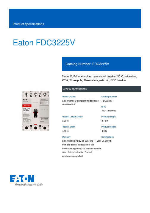
Eaton FDC3225VSeries C, F-frame molded case circuit breaker, 50°C calibration, 225A, Three-pole, Thermal magnetic trip, FDC breakerGeneral specificationsEaton Series C complete molded case circuit breakerFDC3225V 7821141890923.38 in4.13 in 4.13 in 4.5 lb Eaton Selling Policy 25-000, one (1) year from the date of installation of the Product or eighteen (18) months from the date of shipment of the Product, whichever occurs first.UL Listed Product NameCatalog Number UPCProduct Length/Depth Product Height Product Width Product Weight WarrantyCertificationsSeries C200 kAIC at 240 Vac100 kAIC at 480 VacFFDC50 to 60 HzComplete breakerLoad side50°C600 Vac, 250 Vdc225 AFixed thermal, fixed magnetic Three-pole Application of Multi-Wire Terminals for Molded Case Circuit Breakers Application of Tap Rules to Molded Case Breaker TerminalsUL listed 100%-rated molded case circuit breakersPower metering and monitoring with Modbus RTU product aidCircuit breaker motor operators product aidStrandAble terminals product aidMulti-wire lugs product aidMOEM MCCB Product Selection GuideMotor protection circuit breakers product aidPlug-in adapters for molded case circuit breakers product aidCurrent limiting Series C molded case circuit breakers product aid Breaker service centersCounterfeit and Gray Market Awareness GuideEaton's Volume 4—Circuit ProtectionMolded case circuit breakers catalogFDC3 3D Model XchangeTime Current Curves for Series C® F-Frame Circuit BreakersFDC3 3D InventorFDC3 AutoCAD 2D Footprint (mm)Installation Instructions for EHD, EDB, EDS, ED, EDH, EDC, FDB, FD, HFD, FDC, HFDDC Circuit Breakers and Molded Case SwitchesCircuit Breakers ExplainedCircuit breakers explainedSeries C F-Frame molded case circuit breakersEaton Specification Sheet - FDC3225VSeries C J-Frame molded case circuit breakers time current curves Series C G-Frame molded case circuit breakers time current curves MOEM MCCB product selection guideSeriesInterrupt ratingFrameCircuit breaker type Frequency ratingCircuit breaker frame type TerminalsCalibrationVoltage rating Amperage RatingTrip TypeNumber of poles Application notesBrochuresCatalogsDrawingsInstallation instructions MultimediaSpecifications and datasheetsEaton Corporation plc Eaton House30 Pembroke Road Dublin 4, Ireland © 2023 Eaton. All Rights Reserved. Eaton is a registered trademark.All other trademarks areproperty of their respectiveowners./socialmedia。
LTC3350:电容器充电器和备份控制器IC
LTC3350:电容器充电器和备份控制器IC
佚名
【期刊名称】《世界电子元器件》
【年(卷),期】2014(0)7
【摘要】Linear推出LTC3350,该器件是一款超级电容器充电器和备份控制器lC,其包括了组成一个完整、独立和基于电容器的备份电源解决方案必需具备的所有功能。
LTC3350提供所有电源通路(PowerPath)控制、电容器组充电和平衡、以
及电容器“健康状况”监视功能,以确保备份系统能够可靠工作。
【总页数】1页(P24-24)
【关键词】超级电容器;控制器IC;备份控制器;充电器;备份电源;监视功能;电容器组;健康状况
【正文语种】中文
【中图分类】TM53
【相关文献】
1.便携产品选择紧凑型超级电容器充电器IC [J], Steve Knoth
2.双向超级电容器充电器集成了备份和平衡功能 [J], Sam Nork;Steve
Knoth;John Bazinet
3.占板面积仅12mm2的单IC型USB电源管理器、理想二极管控制器和电池充电器 [J],
4.充电器控制器可对任何容量的电容器充电 [J],
5.凌力尔特发布最新超级电容器充电器和备份控制器IC [J],
因版权原因,仅展示原文概要,查看原文内容请购买。
超级电容管理芯片
超级电容管理芯片超级电容管理芯片(Super Capacitor Management Chip,简称SCMC)是一种用于管理和控制超级电容器充放电过程的集成电路芯片。
它通过智能化的控制算法和电路设计,实现对超级电容器的有效管理和保护,提高其性能和可靠性。
超级电容器是一种具有高能量密度、高功率密度和长寿命的电能存储设备。
与传统电池相比,超级电容器具有充电速度快、循环寿命长、无污染、高温工作和可靠性高等优点。
然而,超级电容器也存在一些问题,如电压平衡、充放电控制、过电压保护等方面的挑战。
这就需要使用超级电容管理芯片来解决这些问题。
超级电容管理芯片内部集成了多个功能模块,包括电压检测、电流检测、充放电控制、温度监测、电压平衡等。
其中,电压检测模块用于实时监测超级电容器的电压情况,以确保不会超过额定电压范围。
电流检测模块用于监测超级电容器的充放电电流,以保证电流在安全范围内。
充放电控制模块根据电压和电流的检测结果,控制超级电容器的充放电过程,以确保其在最佳工作状态下运行。
温度监测模块用于监测超级电容器的温度,一旦温度超过设定值,就会采取相应的保护措施。
电压平衡模块则用于平衡超级电容器之间的电压差,以确保各个电容器之间的电压均衡。
超级电容管理芯片还具有多种保护功能,如过电压保护、过电流保护、过温保护等。
当超级电容器的电压、电流或温度超过设定的阈值时,芯片会自动切断电源,以保护超级电容器不受损坏。
此外,超级电容管理芯片还支持通信接口,可以与外部系统进行数据交换和控制。
超级电容管理芯片的应用非常广泛。
在电动车、混合动力车、电动工具等领域,超级电容器被广泛应用于能量存储和回收。
超级电容管理芯片可以提高超级电容器的使用效率和稳定性,延长其使用寿命。
在可再生能源领域,超级电容器和超级电容管理芯片也被用于储能和平滑电网功率。
此外,超级电容管理芯片还可以应用于医疗设备、电子设备、通信设备等领域,提高设备的性能和可靠性。
超级电容充放电管理芯片
超级电容充放电管理芯片超级电容充放电管理芯片是一种专门用于管理超级电容器充放电的芯片。
超级电容器是一种高能量密度的电容器,具有高速充放电、长寿命、高温耐受等优点,因此在许多领域得到了广泛应用,如汽车、电动工具、电子设备等。
然而,超级电容器的充放电过程需要精确的控制,否则容易导致电容器损坏或者电路故障。
这时候,超级电容充放电管理芯片就派上用场了。
它可以通过内部的控制电路,实现对超级电容器的充放电过程进行精确控制,从而保证电容器的安全可靠运行。
超级电容充放电管理芯片的主要功能包括:1. 充电控制:通过内部的充电控制电路,实现对超级电容器的充电过程进行精确控制,从而避免过充或者欠充的情况发生。
2. 放电控制:通过内部的放电控制电路,实现对超级电容器的放电过程进行精确控制,从而避免过放或者欠放的情况发生。
3. 温度控制:通过内部的温度传感器,实时监测超级电容器的温度变化,从而避免因温度过高导致电容器损坏的情况发生。
4. 保护控制:当超级电容器出现异常情况时,如过充、过放、温度过高等,超级电容充放电管理芯片会自动切断电路,从而保护电容器和电路的安全。
超级电容充放电管理芯片的应用范围非常广泛,如汽车、电动工具、电子设备等。
在汽车领域,超级电容器可以作为辅助能量储存装置,用于提供瞬间高功率输出,如启动、加速等。
在电动工具领域,超级电容器可以作为主要能量储存装置,用于提供长时间高功率输出,如电动锤、电动钻等。
在电子设备领域,超级电容器可以作为备用电源,用于提供短时间的电力支持,如计算机、手机等。
超级电容充放电管理芯片是一种非常重要的电子元器件,它可以保证超级电容器的安全可靠运行,为各个领域的应用提供了强有力的支持。
ltc2954的用法
ltc2954的用法LTC2954是一款高性能电源管理芯片,广泛应用于各种电子设备中。
它具有多种功能,可以实现电源开关、电源监控和电源管理等功能,为电子设备的稳定运行提供了重要保障。
首先,LTC2954可以实现电源开关功能。
在很多电子设备中,为了节省能源和延长电池寿命,需要在设备不使用时自动关闭电源。
LTC2954可以通过控制外部开关管,实现电源的开关功能。
当设备不使用时,LTC2954会自动关闭电源,避免电池能量的浪费。
而当设备需要使用时,LTC2954会自动打开电源,保证设备正常运行。
其次,LTC2954还可以实现电源监控功能。
在电子设备中,电源的稳定性对设备的正常运行至关重要。
LTC2954可以监测电源的电压和电流,并及时反馈给控制系统。
当电源电压或电流异常时,LTC2954会发出警报信号,提醒用户或控制系统进行处理。
这样可以避免因电源问题导致的设备故障或损坏,保证设备的稳定运行。
此外,LTC2954还具有电源管理功能。
在一些特殊应用中,需要对电源进行精确控制,以满足设备的特定需求。
LTC2954可以通过外部控制信号,实现对电源的精确控制。
用户可以根据需要,通过控制LTC2954的工作模式和参数,实现对电源的灵活管理。
这样可以满足不同设备的特定需求,提高设备的性能和可靠性。
总之,LTC2954是一款功能强大的电源管理芯片,广泛应用于各种电子设备中。
它可以实现电源开关、电源监控和电源管理等多种功能,为设备的稳定运行提供了重要保障。
通过LTC2954的应用,可以有效节省能源、延长电池寿命,提高设备的性能和可靠性。
未来,随着科技的不断发展,LTC2954的用途将会更加广泛,为电子设备的发展带来更多的可能性。
锂电池线性充电管理芯片LTC4065及其应用
锂电池线性充电管理芯片LTC4065及其应用摘要锂电池具有体积小、能量密度高、无记忆效应、循环寿命高、高电压电池和自放电率低等优点,近年来已经成为微型移动终端设备的首选电源。
本文介绍了基于LTC4065芯片的线性充电管理方案,仅需要非常少的外围元件配合,就可以实现低成本、超小尺寸的单节锂电池充电管理。
关键词锂电池充电管理LTC4065 SG2003随着移动计算技术和无线通信技术的发展,微型移动终端设备在移动数据采集、传输、处理及个人信息服务等领域得到越来越多的应用。
锂电池因其体积小、能量密度高、无记忆效应、循环寿命高、高电压电池和自放电率低等优点,近年来已经成为微型移动终端设备的首选电源。
锂电池的特性以及应用环境的需求,对微型移动终端设备充电方案的设计提出了更高的要求。
因此在充电方案的设计中需要综合考虑成本、体积、噪声、效率等因素。
LTC4065是一款用于单节锂电池的完整恒定电流/恒定电压线性充电管理芯片,可提供高达750 mA且准确度为5%的可设置的充电电流,并支持直接使用USB端口对单节锂电池进行充电。
同时其热反馈功能可调节充电电流,以便在大功率工作或高环境温度条件下对芯片温度加以限制,确保安全工作。
由于采用了内部MOSFET架构,因此无需使用外部检测电阻器或隔离二极管。
很少的外部元件数目加上其2 mm×2 mm DFN封装,使得LTC4065尤其适合无线PDA、蜂窝电话、无线传感器终端等应用。
功能齐全的LTC4065还包括自动再充电、低电池电量充电调节、软启动等丰富功能。
1 LTC4065的引脚功能LTC4065采用了热处理能力较强的6引脚小外形封装(DFN),且实现产品无铅化,底部采用裸露衬垫,直接焊接至PCB以实现电接触和额定散热性能。
引脚排列如图1所示。
各引脚功能如下:引脚1,GND,接地端。
引脚2,CHRG,漏极开路充电状态输出。
充电状态指示引脚具有三种状态:下拉、2 Hz 脉动和高阻抗状态。
引线式超级电容和纽扣式超级电容

引线式超级电容和纽扣式超级电容引线式超级电容和纽扣式超级电容引言超级电容作为一种新型的电化学能量存储设备,由于其高能量密度、快速充放电速度和长寿命等特点,在电子设备、能源存储和汽车电气化等领域展现出了巨大的应用潜力。
其中,引线式超级电容和纽扣式超级电容作为超级电容的两种主要形式,各具特点,应用范围广泛。
本文将全面评估引线式超级电容和纽扣式超级电容的性能、结构、应用及发展前景,以期为读者提供深度和广度兼具的了解。
一、引线式超级电容1. 性能评估引线式超级电容具有高能量密度、长周期寿命和较低的内阻等特点。
其电压范围广,具有较高的额定电压和能量储存量,适用于对能量密度要求较高的场合。
2. 结构分析引线式超级电容通常由正、负极集流体、电极和电解质组成。
引线连接正、负极集流体,电极和电解质通过引线固定,整体结构稳定可靠。
3. 应用领域引线式超级电容广泛应用于智能手机、平板电脑、便携式电子设备等场合,其高能量密度和长寿命特点为这些设备提供了稳定可靠的能量支持。
4. 发展前景引线式超级电容在电子设备领域具有广阔的应用前景,随着技术的不断创新和进步,其在能源存储和汽车电气化领域的应用也将不断扩大。
二、纽扣式超级电容1. 性能评估纽扣式超级电容具有体积小、重量轻、充放电速度快等特点。
其具有较高的功率密度和瞬态响应能力,适用于对快速充放电要求较高的场合。
2. 结构分析纽扣式超级电容采用双层电容结构,电极间嵌入电解质并采用特殊的封装材料密封,结构紧凑且安全可靠。
3. 应用领域纽扣式超级电容常用于医疗器械、智能穿戴设备、无人机等场合,其快速充放电和轻便的特点使得这些设备具有更好的性能表现。
4. 发展前景纽扣式超级电容在智能穿戴设备、物联网和无人机领域具有广阔的应用前景,随着技术的进步和成本的下降,其市场规模将不断扩大。
总结与展望引线式超级电容和纽扣式超级电容各具特点,应用范围广泛,技术不断创新,性能不断提升。
未来,随着新材料、新工艺的引入,超级电容将在能源存储、智能制造等领域展现出更加广阔的应用前景。
ltc2954的用法
LTC2954的用法1. 概述LTC2954是一种低功耗电源管理IC,可用于控制和监测电池供电系统。
它具有多种功能,包括电源开关控制、电池电量检测、系统复位和电源故障检测等。
本文将详细介绍LTC2954的各项功能和使用方法。
2. 功能特点LTC2954具有以下主要功能特点:•电源开关控制:LTC2954可以通过外部触发信号或内部定时器控制电源的开关。
它可以根据需求进行自动开关机控制,提高系统的能效和电池寿命。
•电池电量检测:LTC2954可以监测电池的电量,并提供准确的电量信息。
它采用电流积分技术,可以测量电池的充放电情况,并将电量信息反馈给系统,以便进行电池管理和预警。
•系统复位:LTC2954可以监测系统的电压和电流,并在电源异常或故障时进行系统复位。
它可以检测电压过高、过低、断电等情况,并及时发出复位信号,保护系统的稳定运行。
•电源故障检测:LTC2954可以检测电源故障,如过电流、过温等情况,并及时响应。
它可以通过外部触发信号或内部定时器进行故障检测,并发出警报信号,以便及时处理故障情况。
3. 使用方法LTC2954的使用方法如下:3.1 电源开关控制LTC2954可以通过外部触发信号或内部定时器进行电源开关控制。
通过设置相应的控制寄存器,可以实现自动开关机控制。
例如,设置定时器使LTC2954每隔一定时间检测一次电池电量,当电量低于设定值时,自动关闭电源。
3.2 电池电量检测LTC2954采用电流积分技术进行电池电量检测。
通过测量电池的充放电情况,可以准确计算电池的电量。
可以通过读取相应的寄存器来获取电量信息,并进行电池管理和预警。
3.3 系统复位LTC2954可以监测系统的电压和电流,并在电源异常或故障时进行系统复位。
通过设置复位阈值和延迟时间,可以灵活地配置复位功能。
例如,当电压低于设定值并持续一段时间时,LTC2954会发出复位信号,重启系统。
3.4 电源故障检测LTC2954可以检测电源故障,如过电流、过温等情况,并及时响应。
LTC3225中文资料

13225fTYPICAL APPLICATIONFEATURESAPPLICATIONSDESCRIPTIONChargerThe L TC ®3225 is a programmable supercapacitor charger designed to charge two supercapacitors in series to a fi xed output voltage (4.8V/5.3V selectable) from a 2.8V/3V to 5.5V input supply. Automatic cell balancing prevents overvoltage damage to either supercapacitor . No balancing resistors are required.Low input noise, low quiescent current and low external parts count (one fl ying capacitor , one bypass capacitor at V IN and one programming resistor) make the L TC3225 ideally suited for small battery-powered applications.Charging current level is programmed with an external resistor . When the input supply is removed, the L TC3225 automatically enters a low current state, drawing less than 1μA from the supercapacitors.The L TC3225 is available in a 10-lead 3mm × 2mm DFN package.nLow Noise Constant Frequency Charging of T wo Series Supercapacitorsn Automatic Cell Balancing Prevents Capacitor Overvoltage During Chargingn Programmable Charging Current (Up to 150mA)n Selectable 2.4V or 2.65V Regulation per Cell n Automatic Recharge n I VIN = 20μA in Standby Mode n I COUT < 1μA When Input Supply is Removed n No Inductorsn Tiny Application Circuit (3mm × 2mm DFN Package, All Components <1mm High)nCurrent Limited Applications with High Peak Power Loads (LED Flash, PCMCIA Tx Bursts, HDD Bursts, GPRS/GSM T ransmitter)n Backup SuppliesCharging Profi le with 30% Mismatchin Output Capacitance, C TOP < C BOTL , L T , L TC and L TM are registered trademarks of Linear Technology Corporation. All other trademarks are the property of their respective owners.OUTV IN2.8V/3V TO 5.5VSHDN 5V/DIV V COUT 2V/DIVV TOP -V BOT 200mV/DIVI VIN300mA/DIV5s/DIV 3225 TA01bV SEL = V INR PROG = 12k C TOP = 1.1F C BOT = 1.43FC TOP INITIAL VOL TAGE = 0V C BOT INITIAL VOL TAGE = 0V23225fPIN CONFIGURATIONABSOLUTE MAXIMUM RATINGSV IN , C OUT to GND .........................................–0.3V to 6V SHDN , V SEL ......................................–0.3V to V IN + 0.3VC OUT Short-Circuit Duration .............................Indefinite I VIN Continuous (Note 2) ......................................350mA I OUT Continuous (Note 2) .....................................175mA Operating Temperature Range (Note 3)....–40°C to 85°C Storage Temperature Range ...................–65°C to 125°C(Note 1)TOP VIEW 11DDB PACKAGE10-LEAD (3mm s 2mm) PLASTIC DFN C +C –CX SHDN PGOOD C OUT V IN GND PROG V SEL68791054231T JMAX = 125°C, θJA = 76°C/WEXPOSED PAD (PIN 11) MUST BE SOLDERED TO LOW IMPEDANCE GND PLANE (PIN 8) ON PCBORDER INFORMATIONELECTRICAL CHARACTERISTICS SYMBOL PARAMETERCONDITIONS MIN TYP MAX UNITSV IN-UVLO Input Supply Undervoltage LockoutHigh-to-Low ThresholdV SEL = V IN V SEL = 0l l2.652.42.752.5 2.852.6V V V IN-UVLO-HYS Input Supply Undervoltage Lockout Hysteresis V SEL = V IN V SEL = 0150140mV mVV IN Input Voltage RangeV SEL = V IN V SEL = 0V l l 32.8 5.55.5V V V COUT Charge Termination VoltageSleep Mode Threshold (Rising Edge)V SEL = V IN V SEL = 0Vl l 5.24.75.34.8 5.44.9V V V COUT-HYS Output Comparator Hysteresis 100mV V TOP/BOT Maximum Voltage Across Each of the Supercapacitors After Charging V SEL = V IN V SEL = 0V l l 2.752.5V V I Q-VIN No Load Operating Current at V IN I OUT = 0mAl 2040μA I SHDN-VIN Shutdown Current SHDN = 0V , V OUT = 0Vl 0.11μA I COUTC OUT Leakage CurrentV OUT = 5.6V , SHDN = 0VV OUT = 5.6V , Charge Pump in Sleep Mode V OUT = 5.6V , SHDN Connected to V IN with Input Supply Removedl l12341μA μA μA I VINInput Charging Current V IN = 3.6V , R PROG = 12k, C TOP = C BOT 306mA V IN = 3.6V , R PROG = 60k, C TOP = C BOT55mAThe l denotes the specifi cations which apply over the full operatingtemperature range, otherwise specifi cations are at T A = 25°C. V IN = 3.6V , C IN = 2.2μF , C FL Y = 1μF , unless otherwise specifi ed.Lead Free FinishTAPE AND REEL (MINI)TAPE AND REELPART MARKINGPACKAGE DESCRIPTIONTEMPERATURE RANGE L TC3225EDDB#TRMPBF L TC3225EDDB#TRPBF LCYR 10-Lead (3mm × 2mm) Plastic DFN –40°C to 85°CTRM = 500 pieces.Consult L TC Marketing for parts specifi ed with wider operating temperature ranges.Consult L TC Marketing for information on lead based fi nish parts.For more information on lead free part marking, go to: http://www.linear .com/leadfree/For more information on tape and reel specifi cations, go to: http://www.linear .com/tapeandreel/33225fSYMBOL PARAMETERCONDITIONSMIN TYP MAX UNITS I OUTOutput Charging CurrentV IN = 3.6V , R PROG = 12k, V OUT = 4.5V ,C TOP = C BOT125150175mA V IN = 3.6V , R PROG = 60k, V OUT = 4.5V , C TOP = C BOT26mAV PGOOD PGOOD Low Output VoltageI PGOOD = –1.6mA l 0.4V I PGOOD-LEAK PGOOD High Impedance Leakage Current V PGOOD = 5Vl 10μA V PG PGOOD Low-to-High Threshold Relative to Output Voltage Threshold l 929496%V PG-HYS PGOOD Threshold Hysteresis Relative to Output Voltage Threshold l0.251.22.5%R OL Effective Open-Loop Output Impedance (Note 4)V IN = 3.6V , V OUT = 4.5V8Ωf OSC CLK Frequencyl 0.60.9 1.5MHz V SEL , SHDN V IH Input High Voltage l 1.3VV IL Input Low Voltage l 0.4V I IH Input High Current l –11μA I ILInput Low Currentl–11μAELECTRICAL CHARACTERISTICS The l denotes the specifi cations which apply over the full operatingtemperature range, otherwise specifi cations are at T A = 25°C. V IN = 3.6V , C IN = 2.2μF , C FL Y = 1μF , unless otherwise specifi ed.Note 1: Stresses beyond those listed under Absolute Maximum Ratings may cause permanent damage to the device. Exposure to any Absolute Maximum Rating condition for extended periods may affect device reliabilty and lifetime.Note 2: Based on long-term current density limitations.Note 3: The L TC3225 is guaranteed to meet performance specifi cations from 0°C to 85°C. Specifi cations over the –40°C to 85°C operatingtemperature range are assured by design, characterization and correlation with statistical process controls. Note 4: Output not in regulation; R OL ≡ (2 • V IN – V OUT )/I OUTTYPICAL PERFORMANCE CHARACTERISTICSI OUT vs R PROGEffi ciency vs V IN(T A = 25°C, C FL Y = 1μF , C IN = 2.2μF , C TOP = C BOT , unless otherwise specifi ed)I OUT vs V OUT (R PROG = 12k)R PROG (kΩ)010I O U T (m A )60801004070603225 G0140200203050120140160V OUT (V)0I O U T (m A )2060801002451803225 G0240130.52.5 4.51.53.5120140160V IN (V)2.5E F F I C I E N C Y (%)10304050 4.5100903525 G0320 3.5354 5.560708043225fOscillator Frequency vs Supply VoltageCharge Pump Open-Loop Output Resistance vs Temperature (2V IN – V COUT )/I OUTTYPICAL PERFORMANCE CHARACTERISTICS(T A = 25°C, C FL Y = 1μF , C IN = 2.2μF , C TOP = C BOT , unless otherwise specifi ed)I OUT (mA)020457801203225 G04324060100140160106E X T R A I I N (m A )V IN (V)2.50I I N (μA )5101520303 3.54 4.53225 G055 5.525V IN20mV/DIV I VIN200mA/DIV200ns/DIV3225 G06R PROG = 12k0mACharging Profi le with Unequal Initial Output Capacitor Voltage (Initial V TOP = 1.3V , V BOT = 1V)V IN (V)2.50.88F R E Q U E N C Y (M H z )0.890.910.9233.54 4.53225 G0750.930.940.90 5.5TEMPERATURE (°C)–40R O L (Ω)6810603225 G0842579310–15103585SHDN 5V/DIV V COUT 2V/DIV V TOP -V BOT 500mV/DIVI VIN300mA/DIV2s/DIV 3225 G09V SEL = V INR PROG = 12kC TOP = C BOT = 1.1FExtra Input Current vs OutputCurrent (I VIN – 2 • I OUT )No-Load Input Current vs Supply VoltageInput Ripple and Input CurrentCharging Profi le with Unequal Initial Output Capacitor Voltage (Initial V TOP = 1V , V BOT = 1.3V)SHDN 5V/DIV V COUT 2V/DIV V TOP -V BOT 500mV/DIVI VIN300mA/DIV2s/DIV3225 G10V SEL = V INR PROG = 12kC TOP = C BOT = 1.1FSHDN 5V/DIV V COUT 2V/DIV V TOP -V BOT 200mV/DIVI VIN300mA/DIV5s/DIV 3225 G11V SEL = V INR PROG = 12k CTOP = 1.43F C BOT = 1.1FC TOP INITIAL VOL TAGE = 0V C BOT INITIAL VOL TAGE = 0VSHDN 5V/DIV V COUT 2V/DIV V TOP -V BOT 200mV/DIVI VIN300mA/DIV5s/DIV 3225 G12V SEL = V INR PROG = 12k CTOP = 1.1F C BOT = 1.43FC TOP INITIAL VOL TAGE = 0V C BOT INITIAL VOL TAGE = 0VCharging Profi le with 30%Mismatch in Output Capacitance (C TOP > C BOT )Charging Profi le with 30%Mismatch in Output Capacitance (C TOP < C BOT )PIN FUNCTIONSC+ (Pin 1): Flying Capacitor Positive Terminal. A 1μF X5R or X7R ceramic capacitor should be connected from C+ to C–.C– (Pin 2): Flying Capacitor Negative Terminal.CX (Pin 3): Midpoint of T wo Series Supercapacitors. This pin voltage is monitored and forced to track C OUT (CX = C OUT/2) during charging to achieve voltage balancing of the top and bottom supercapacitors.SHDN (Pin 4): Active Low Shutdown Input. A low on SHDN puts the L TC3225 in low current shutdown mode. Do not fl oat the SHDN pin.PGOOD (Pin 5): Open-Drain Output Status Indicator. Upon start-up, this open-drain pin remains low until the output voltage, V OUT, is within 6% (typical) of its fi nal value. Once V OUT is valid, PGOOD becomes Hi-Z. If V OUT falls 7.2% (typical) below its correct regulation level, PGOOD is pulled low. PGOOD may be pulled up through an external resistor to an appropriate reference level. This pin is Hi-Z in shutdown mode.V SEL (Pin 6): Output Voltage Selection Input. A logic low at V SEL sets the regulated C OUT to 4.8V; a logic high sets the regulated C OUT to 5.3V. Do not fl oat the V SEL pin. PROG (Pin 7): Charging Current Programming Pin. A resis-tor connected between this pin and GND sets the charging current. (See Applications Information section).GND (Pin 8): Charge Pump Ground. This pin should be connected directly to a low impedance ground plane.V IN (Pin 9): Power Supply for the L TC3225. V IN should be bypassed to GND with a low ESR ceramic capacitor of more than 2.2μF.C OUT (Pin 10): Charge Pump Output Pin. Connect C OUT to the top plate of the top supercapacitor. C OUT provides charge current to the supercapacitors and regulates the fi nal voltage to 4.8V/5.3V.Exposed Pad (Pin 11): This pad must be soldered to a low impedance ground plane for optimum thermal performance.53225fSIMPLIFIED BLOCK DIAGRAMTOPBOT3225 F01Figure 163225fOPERATIONThe L TC3225 is a dual cell supercapacitor charger. Its unique topology maintains a constant output voltage with programmable charging current. Its ability to maintain equal voltages on both cells while charging protects the supercapacitors from damage that is possible with other charging methods, without the use of external balancing resistors. The L TC3225 includes an internal switched capacitor charge pump to boost V IN to a regulated output voltage. A unique architecture maintains relatively constant input current for the lowest possible input noise. The basic charger circuit requires only three external components. Normal Charge CycleOperation begins when the SHDN pin is pulled above 1.3V. The C OUT pin voltage is sensed and compared with a preset voltage threshold using an internal resistor divider and a comparator. The preset voltage threshold is 4.8V/5.3V selectable with the V SEL pin. If the voltage at the C OUT pin is lower than the preset voltage threshold, the oscillator is enabled. The oscillator operates at a typical frequency of 0.9MHz. When the oscillator is enabled, the charge pump operates charging up C OUT. The input current drawn by the internal charge pump ramps up at approximately 20mA/μs each time the charge pump starts up from shutdown. Once the output voltage is charged to the preset voltage threshold, the part shuts down the internal charge pump and enters into a low current state. In this state, the L TC3225 consumes only about 20μA from the input supply. The current drawn from C OUT is approximately 2μA. Automatic Cell BalancingThe L TC3225 constantly monitors the voltage across both supercapacitors while charging. When the voltage across the supercapacitors is equal, both capacitors are charged with equal currents. If the voltage across one supercapacitor is lower than the other, the lower supercapacitor’s charge current is increased and the higher supercapacitor’s charge current is decreased. The greater the difference between the supercapacitor voltages, the greater the difference in charge current per capacitor. The charge currents can increase or decrease as much as 50% to balance the volt-age across the supercapacitors. When the cell voltages are balanced, the supercapacitors are charged at a rate of approximately:I ICOUT VIN=12•If the leakage currents or capacitances of the two su-percapacitors are mismatched enough that varying the charging current is not suffi cient to balance their volt-ages, the L TC3225 stops charging the capacitor with the higher voltage until they are again balanced. This feature protects either capacitor from experiencing an overvoltage condition.Shutdown ModeAsserting SHDN low causes the L TC3225 to enter shut-down mode. When the charge pump is fi rst disabled, the L TC3225 draws approximately 1μA of supply current from V IN and C OUT. After V OUT is discharged to 0V, the current from V IN drops to less than 1μA. With SHDN connected to V IN, the output sinks less than 1μA when the input sup-ply is removed. Since the SHDN pin is a high impedance CMOS input, it should never be allowed to fl oat. Output Status Indicator (PGOOD)During shutdown, the PGOOD pin is high impedance. When the charge cycle starts, an internal N-channel MOSFET pulls the PGOOD pin to ground. When the output voltage, V OUT, is within 6% (typical) of its fi nal value, the PGOOD pin becomes high impedance, but charge current continues to fl ow until V OUT crosses the charge termination voltage. When V OUT drops 7% below the charge termination volt-age, the PGOOD pin again pulls low.Current Limit/Thermal ProtectionThe L TC3225 has built-in current limit as well as overtem-perature protection. If the PROG pin is shorted to ground, a protection circuit automatically shuts off the internal charge pump. At higher temperatures, or if the input voltage is high enough to cause excessive self-heating of the part, the thermal shutdown circuitry shuts down the charge pump once the junction temperature exceeds approximately 150°C. It will enable the charge pump once the junction temperature drops back to approximately 135°C. The L TC3225 is able to cycle in and out of thermal shutdown indefi nitely without latch-up or damage until the overcurrent condition is removed.73225f83225fAPPLICATIONS INFORMATIONProgramming Charge CurrentThe charging current is programmed with a single resistor connecting the PROG pin to ground. The program resistor and the input/output charge currents are calculated using the following equations:I V R I IVIN PROGOUTVIN ==36002(with matched outp p ut capacitors)An R PROG resistor value of 2k or less (i.e., short circuit) causes the L TC3225 to enter overcurrent shutdown mode. This mode prevents damage to the part by shutting down the internal charge pump.Power Effi ciencyThe power effi ciency (η) of the L TC3225 is similar to that of a linear regulator with an effective input voltage of twice the actual input voltage. In an ideal regulating voltage doubler the power effi ciency is given by:η222xIDEAL OUT IN OUT OUT IN OUT OUTI P P V I V I V V ===••NAt moderate to high output power the switching losses and quiescent current of the L TC3225 are negligible and the above expression is valid. For example, with V IN = 3.6V , I OUT = 100mA and V OUT regulated to 5.3V , the measured effi ciency is 71.2% which is in close agreement with the theoretical 73.6% calculation.Effective Open-Loop Output Resistance (R OL )The effective open-loop output resistance (R OL ) of a charge pump is an important parameter that describes the strength of the charge pump. The value of this parameter depends on many factors including the oscillator frequency (f OSC ), value of the fl ying capacitor (C FL Y ), the non-overlap time,the internal switch resistances (R S ) and the ESR of the external capacitors. Output Voltage ProgrammingThe L TC3225 has a V SEL input pin that allows the user to set the output threshold voltage to either 4.8V or 5.3V by forcing a low or high at the V SEL pin respectively.Charging Time EstimationThe estimated charging time when the initial voltage across the two output supercapacitors is equal is given by the equation:t C V V I CHRG OUT COUT INIOUT=()•–where C OUT is the series output capacitance, V COUT is thevoltage threshold set by the V SEL pin, V INI is the initial voltage at the C OUT pin and I OUT is the output charging current given by:I V R OUT PROG=1800When the charging process starts with unequal initialvoltages across the output supercapacitors, only the ca-pacitor with the lower voltage level is charged; the other capacitor is not charged until the voltages equalize. This extends the charging time slightly. Under the worst-case condition, whereby one capacitor is fully depleted while the other remains fully charged due to signifi cant leakage current mismatch, the charging time is about 1.5 times longer than normal. Thermal ManagementFor higher input voltages and maximum output current, there can be substantial power dissipation in the L TC3225. If the junction temperature increases above approximately150°C, the thermal shutdown circuitry automatically deactivates the output. To reduce the maximum junction temperature, a good thermal connection to the PC board is recommended. Connecting the GND pin (Pin 8) and the Exposed Pad (Pin 11) of the DFN package to a ground plane under the device on two layers of the PC board can reduce the thermal resistance of the package and PC board considerably.V IN Capacitor SelectionThe type and value of C IN controls the amount of ripple present at the input pin (V IN). To reduce noise and ripple, it is recommended that low equivalent series resistance (ESR) multilayer ceramic chip capacitors (MLCCs) be used for C IN. Tantalum and aluminum capacitors are not recommended because of their high ESR.The input current to the L TC3225 is relatively constant dur-ing both the input charging phase and the output charging phase but drops to zero during the clock non-overlap times. Since the non-overlap time is small (~40ns) these missing “notches” result in only a small perturbation on the input power supply line. Note that a higher ESR capacitor, such as a tantalum, results in higher input noise. Therefore, ceramic capacitors are recommended for their exceptional ESR performance. Further input noise reduction can be achieved by powering the L TC3225 through a very small series inductor as shown in Figure 2.A 10nH inductor will reject the fast current notches, thereby presenting a nearly constant current load to the input power supply. For economy, the 10nH inductor can be fabricated on the PC board with about 1cm (0.4") of PC board trace.Flying Capacitor SelectionWarning: Polarized capacitors such as tantalum or alumi-num should never be used for the fl ying capacitor since it s volt age can reverse upon st art-up of t he LTC3225. Low ESR ceramic capacitors should always be used for the fl ying capacitor.The fl ying capacitor controls the strength of the charge pump. In order to achieve the rated output current, it is necessary to use at least 0.6μF of capacitance for the fl ying capacitor.The effective capacitance of a ceramic capacitor varies with temperature and voltage in a manner primarily determined by its formulation. For example, a capacitor made of X5R or X7R material retains most of its capacitance from –40°C to 85°C whereas a Z5U or Y5V type capacitor loses considerable capacitance over that range. X5R, Z5U and Y5V capacitors may also have a poor voltage coeffi cient causing them to lose 60% or more of their capacitance when the rated voltage is applied. Therefore, when com-paring different capacitors, it is often more appropriate to compare the amount of achievable capacitance for a given case size rather than comparing the specifi ed capacitance value. For example, over rated voltage and temperature conditions, a 4.7μF 10V Y5V ceramic capacitor in a 0805 case may not provide any more capacitance than a 1μF 10V X5R or X7R capacitor available in the same 0805 case. In fact, over bias and temperature range, the 1μF 10V X5R or X7R provides more capacitance than the 4.7μF 10V Y5V capacitor. The capacitor manufacturer’s data sheet should be consulted to determine what value of capacitor is needed to ensure minimum capacitance values are met over operating temperature and bias voltage.V INFigure 2. 10nH Inductor Used for Input Noise Reduction APPLICATIONS INFORMATION93225f103225fTYPICAL APPLICATIONTable 1 contains a list of ceramic capacitor manufacturers and how to contact them.Table 1. Capacitor ManufacturersAVX Kemet Murata Taiyo Yuden Vishay TDKLayout ConsiderationsDue to the high switching frequency and high transient currents produced by the L TC3225, careful board layout is necessary for optimum performance. An unbroken ground plane and short connections to all the external capacitors improves performance and ensures proper regulation under all conditions.The voltages on the fl ying capacitor pins C + and C – have very fast rise and fall times. The high dv/dt values on these pins can cause energy to capacitively couple to adjacent printed circuit board traces. Magnetic fi elds can also be generated if the fl ying capacitors are far from the part (i.e. the loop area is large). To prevent capacitive energy transfer , a Faraday shield may be used. This is a grounded PC trace between the sensitive node and the L TC3225 pins. For a high quality AC ground it should be returned to a solid ground plane that extends all the way to the L TC3225.Table 2. Supercapacitor ManufacturersCAP-XX NESS CAP Maxwell Bussmann AVXAPPLICATIONS INFORMATION5V Supercapacitor Backup SupplyO VLTC3225113225fInformation furnished by Linear Technology Corporation is believed to be accurate and reliable. However , no responsibility is assumed for its use. Linear Technology Corporation makes no representa-tion that the interconnection of its circuits as described herein will not infringe on existing patent rights.PACKAGE DESCRIPTIONDDB Package10-Lead Plastic DFN (3mm × 2mm)(Reference L TC DWG # 05-08-1722 Rev Ø)NOTE:1. DRAWING CONFORMS TO VERSION (WECD-1) IN JEDEC PACKAGE OUTLINE M0-2292. DRAWING NOT TO SCALE3. ALL DIMENSIONS ARE IN MILLIMETERS4. DIMENSIONS OF EXPOSED PAD ON BOTTOM OF PACKAGE DO NOT INCLUDEMOLD FLASH. MOLD FLASH, IF PRESENT, SHALL NOT EXCEED 0.15mm ON ANY SIDE 5. EXPOSED PAD SHALL BE SOLDER PLATED6. SHADED AREA IS ONLY A REFERENCE FOR PIN 1 LOCATION ON THE TOP AND BOTTOM OF PACKAGEBOTTOM VIEW—EXPOSED PAD(DDB10) DFN 0905 REV ØPIN 1R = 0.20 OR 0.25s 45o CHAMFERRECOMMENDED SOLDER PAD PITCH AND DIMENSIONSLTC3225123225fLinear Technology Corporation1630 McCarthy Blvd., Milpitas, CA 95035-7417(408) 432-1900 ● FAX: (408) 434-0507 ● © LINEAR TECHNOLOGY CORPORA TION 2008LT 0508 • PRINTED IN USARELATED PARTSTYPICAL APPLICATIONPART NUMBERDESCRIPTIONCOMMENTSL TC1751-3.3/L TC1751-5Micropower 5V/3.3V Doubler Charge Pumps I Q = 20μA, Up to 100mA Output, SOT-23 Package L TC1754-3.3/L TC1754-5Micropower 5V/3.3V Doubler Charge Pumps I Q = 13μA, Up to 50mA Output, SOT-23 Package L TC3200Constant Frequency Doubler Charge Pump Low Noise, 5V Output or AdjustableL TC3203/L TC3203B/L TC3203B-1/L TC3203-1500mA Low Noise High Effi ciency Dual Mode Step-Up Charge PumpsV IN : 2.7V to 5.5V , 3mm × 3mm 10-Lead DFN Package L TC3204/L TC3204B-3.3/L TC3204-5Low Noise Regulating Charge Pumps Up to 150mA (L TC3204-5), Up to 50mA (L TC3204-3.3)L TC3221/L TC3221-3.3/L TC3221-5Micropower Regulated Charge Pump Up to 60mA OutputL TC3240-3.3/L TC3240-2.5Step-Up/Step-Down Regulated Charge Pumps Up to 150mA OutputL T ®3420/L T3420-1 1.4A/1A Photofl ash Capacitor Charger with Automatic Top-Off Charges 220μF to 320V in 3.7 Seconds from 5V , V IN : 2.2V to 16V , I SD < 1μA, 10-Lead MS PackageL T3468/L T3468-1/L T3468-21.4A/1A/0.7A, Photofl ash Capacitor Charger V IN :2.5V to 16V , Charge Time = 4.6 Seconds for the L T3468 (0V to 320V , 100μF , V IN =3.6V), I SD < 1μA, ThinSOT TM PackageL TC3484-0/L TC3484-1/ L TC3484-21.4A/0.7A/1A, Photofl ash Capacitor ChargerV IN : 1.8V to 16V , Charge Time = 4.6 Seconds for the L T3484-0 (0V to 320V , 100μF , V IN = 3.6V), I SD < 1μA, 2mm × 3mm 6-Lead DFN PackageL T3485-0/L T3485-1/ L T3485-2/L T3485-31.4A/0.7A/1A/2A Photofl ash Capacitor Chargerwith Output Voltage Monitor and Integrated IGBTV IN : 1.8V to 10V , Charge Time = 3.7 Seconds for the L T3485-0 (0V to 320V , 100μF , V IN = 3.6V), I SD < 1μA, 3mm × 3mm 10-Lead DFN Driver L T3750Capacitor Charger Controller Charges Any Size Capacitor , 10-Lead MS PackageThinSOT is a trademark of Linear Technology Corporation.V BIAS 3.3V V IN 12VGNDGNDL T3740HIGH EFFICIENCY D1CSHD6-40C 12V Supercapacitor Backup Supply。
LTC2655特性-应用
LTC2655特性/应用
描述
LTC®2655是一个4 通道、I2C、16 位/ 12 位、轨至轨DAC 系列,具有集成10ppm/?C 最大值基准。
这些DAC 具有内置的高性能、轨至轨输出缓冲器,并保证具有单调特性。
LTC2655-L 具有一个 2.5V 的全标度输出和集成基准,并采用 2.7V 至 5.5V 的单工作电源。
LTC2655-H 具有一个 4.096V 的全标度输出和集成基准,并采用 4.5V 至 5.5V 的单工作电源。
每个DAC 也可以采用一个外部基准来运作,该外部基准负责将DAC 全标度输出设定为外部基准电压的两倍。
这些器件采用二线式I2C 兼容型串行接口。
LTC2655 工作于标准模式(最大时钟频率为100kHz) 和快速模式(最大时钟频率为400kHz)。
LTC2655 包括一个受控于PORSEL 引脚的上电复位电路。
如果PORSEL 引脚连接至GND,则DAC 在上电时被复位至零标度。
如果PORSEL 引脚连接至VCC,则DAC 在上电时将被复位至中间标度。
特点
●集成10ppm/uC 最大值基准
●最大INL 误差:±4LSB (在16 位)
●在整个温度范围内保证单调
●可选择的内部或外部基准
●2.7V至5.5V 电源范围(LTC2655-L)
●集成基准缓冲器
●DAC之间的超低串扰(1nVus)
●上电复位至零标度/中间标度。
贴片电感3225
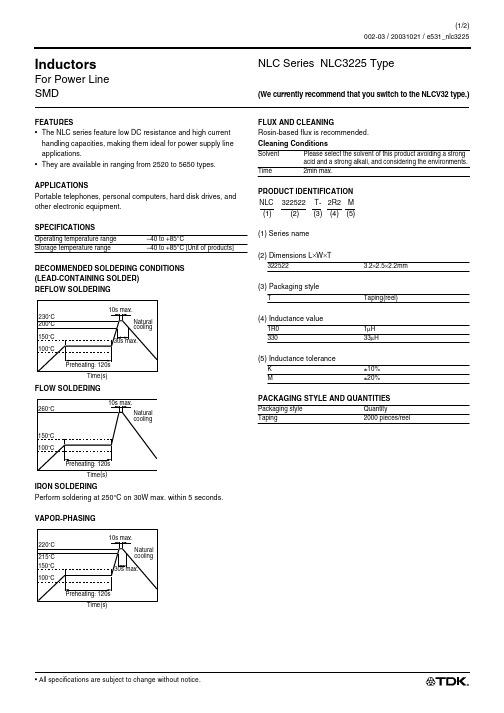
100 Inductance (µH) 50
47µH 22µH 10µH
10 5
1 0.5 1 1µH 0.1 current (mA)
500 1000
0.5
1
5 10 Frequency (MHz)
50 100
• All specifications are subject to change without notice.
Operating temperature range Storage temperature range –40 to +85°C –40 to +85°C [Unit of products]
NLC Series NLC3225 Type
(We currently recommend that you switch to the NLCV32 type.)
FLUX AND CLEANING Rosin-based flux is recommended. Cleaning Conditions
Solvent Time Please select the solvent of this product avoiding a strong acid and a strong alkali, and considering the environments. 2min max.
2.5±0.2
1.2 2
1.9±0.1
Weight: 50mg
2 1.2 Dimensions in mm
ELECTRICAL CHARACTERISTICS
超级电容充放电管理芯片
超级电容充放电管理芯片超级电容充放电管理芯片是一种能够对电容器进行充放电管理的芯片,其具有高效、稳定、可靠等优点,被广泛应用于各种领域。
本文将从超级电容充放电管理芯片的原理、特点、应用等方面进行阐述。
一、超级电容充放电管理芯片的原理超级电容充放电管理芯片的原理是通过对电容器的电压、电流进行控制,实现电容器的充放电管理。
具体来说,当电容器需要充电时,芯片会通过控制电压源的输出电压,使电容器的电压逐渐上升,直到达到设定的充电电压;当电容器需要放电时,芯片会通过控制电流源的输出电流,使电容器的电流逐渐减小,直到电容器的电压下降到设定的放电电压。
超级电容充放电管理芯片的充放电过程是自动化的,不需要人工干预,具有高效、稳定、可靠等优点。
此外,由于芯片能够对电容器的电压、电流进行精细控制,因此可以有效地延长电容器的使用寿命。
二、超级电容充放电管理芯片的特点1. 高效性超级电容充放电管理芯片具有高效性,能够实现快速充放电,提高了电容器的使用效率。
2. 稳定性超级电容充放电管理芯片具有稳定性,能够对电容器的电压、电流进行精细控制,保证了充放电过程的稳定性。
3. 可靠性超级电容充放电管理芯片具有可靠性,能够自动化地进行充放电管理,减少了人工干预的风险,保证了电容器的安全运行。
4. 精度高超级电容充放电管理芯片具有精度高的特点,能够对电容器的电压、电流进行精细控制,保证了充放电过程的精度。
5. 成本低超级电容充放电管理芯片的成本相对较低,能够降低电容器的使用成本。
三、超级电容充放电管理芯片的应用超级电容充放电管理芯片广泛应用于各种领域,例如:1. 新能源汽车超级电容充放电管理芯片能够对新能源汽车中的超级电容器进行充放电管理,提高了电池的使用效率和寿命,延长了电池的使用寿命。
2. 电子设备超级电容充放电管理芯片能够对电子设备中的电容器进行充放电管理,提高了电子设备的使用效率和稳定性,延长了电子设备的使用寿命。
3. 通信设备超级电容充放电管理芯片能够对通信设备中的电容器进行充放电管理,提高了通信设备的使用效率和稳定性,延长了通信设备的使用寿命。
LTC3588应用电路(压电式能量收集电源)
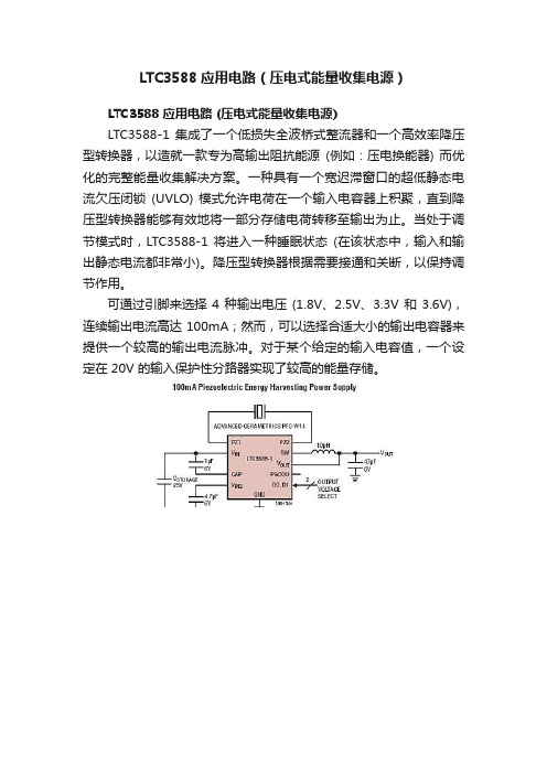
LTC3588应用电路(压电式能量收集电源)
LTC3588应用电路 (压电式能量收集电源)
LTC3588-1 集成了一个低损失全波桥式整流器和一个高效率降压型转换器,以造就一款专为高输出阻抗能源(例如:压电换能器) 而优化的完整能量收集解决方案。
一种具有一个宽迟滞窗口的超低静态电流欠压闭锁(UVLO) 模式允许电荷在一个输入电容器上积聚,直到降压型转换器能够有效地将一部分存储电荷转移至输出为止。
当处于调节模式时,LTC3588-1 将进入一种睡眠状态(在该状态中,输入和输出静态电流都非常小)。
降压型转换器根据需要接通和关断,以保持调节作用。
可通过引脚来选择4 种输出电压(1.8V、2.5V、3.3V 和3.6V),连续输出电流高达 100mA;然而,可以选择合适大小的输出电容器来提供一个较高的输出电流脉冲。
对于某个给定的输入电容值,一个设定在 20V 的输入保护性分路器实现了较高的能量存储。
超级电容规格书说明书

HCCCAP EDLCsSPECIFICATION HCCCAP超级电容规格书【PRODUCT】产品:HCCCAP EDLCs【MODEL】型号:HCAP-C2R7166北京合众汇能科技有限公司HCC ENERGY TECH.Co.,LTD.TEL:+86-10-82897371email:*******************1.适用范围Scope本产品规格书对产品的性能,测试方法进行了规范,作为技术确认的参照。
数据参数仅作参考,不同批次与不同时间生产的实际产品参数可能会有所变化,以实际收到的产品为准,确切参数请及时向厂家核实。
This specification describes,the product property and test method,and should serve as the reference for technical assurance.These data is only for reference,actual product data in different batches and different times may vary,with the actual receipt of the product as a prospective,exact parameters,please promptly to the manufacturers to verify.2.一般特性General Specifications1)产品性能Features●高能量密度Ultra High Energy Density●长寿命Long Usage Life●高低温性能Excellent Performance at High and Low Temperatures●环保Environmental Friendly●免维护Maintenance Free2)产品应用范围Typical Applications●智能电网及其它配套设备Smart grid and other ancillary equipment●智能三表Intelligent Three-ammeters●集中器Concentrator●故障指示器Fault Indicator●混合动力汽车HEV/EV●太阳能/风能Solar/Wind energy●电机启动Motor drive●后备电源Memory Back up Batteries3)标准测试条件在标准大气压,温度5~35℃,相对湿度小于85%条件下进行测试;本规格书标准测试条件为标准大气压,温度25℃,相对湿度小于60%。
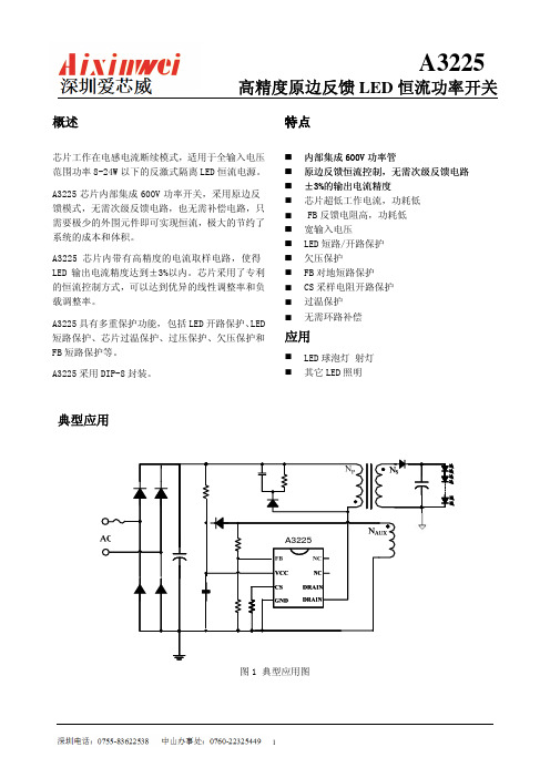
驱动IC A3225规格书
OVP 电压门限对温度的变化
5
启动电流对温度的变化
A 3225
高精度原边反馈 LED 恒流功率开关
电流检测门限对温度的变化
内部结构框图
图 3 A3225 内部框图
6
A 3225
高精度原边反馈 LED 恒流功率开关
应用信息
A3225 是一款专用于 LED 照明的恒流驱动芯片, 采用专利的恒流架构和控制方法,芯片内部集成 600V 功率开关,只需要极少的外围组件就可以达 到优异的恒流特性。无需光耦及 TL431 反馈,系 统成本低。
490
500
510
mV
500
ns
200
ns
工作电流 IST IOP
FB 反馈 VFB
TDemag_Min ΔVCS/ΔIFB_up
Байду номын сангаас
启动电流 典型工作电流
FB 反馈电压阈值 最小退磁时间 线电压补偿比例
VCC= VCC_th - 1V FOP =40KHz
(注 6)
25
50
uA
1.5
mA
1
V
4
us
1.1
保证满足个别性能指标。电气参数定义了器件在工作范围内并且在保证特定性能指标的测试条件下的直流和交流电参数 规范。对于未给定上下限值的参数,该规范不予保证其精度,但其典型值合理反映了器件性能。
注 2:温度升高最大功耗一定会减小,这也是由 TJMAX, θJA,和环境温度 TA 所决定的。最大允许功耗为 PDMAX = (TJMAX TA)/ θJA 或是极限范围给出的数字中比较低的那个值。 注 3:人体模型,100pF 电容通过 1.5KΩ 电阻放电。
当输出出现 LED 短路或 LED 开路时,系统将自动 进入低功耗模式,同时不断检测负载状态,直到 故障解除。当故障解除后,系统自动恢复正常工 作。
一点创绘超级电容充放电模块用户使用手册
标题:一点创绘超级电容充放电模块用户使用手册一、前言在现代科技发展迅速的今天,电力储存与管理已经成为各行业关注的焦点话题。
超级电容作为一种新型的存储设备,其高能量密度和长寿命等优势逐渐受到人们的关注。
一点创绘超级电容充放电模块作为一种应用于电子设备的重要组件,其使用手册也尤为重要。
二、产品概述一点创绘超级电容充放电模块是一种集成了充电和放电功能的超级电容模块。
其主要特点包括高效、稳定、安全等特点,可以广泛应用于电子设备、储能系统等领域。
三、产品性能参数1. 输入电压范围:在这一点上,建议用户仔细阅读产品手册,并根据产品手册上的操作指引进行操作,以免发生不必要的误操作;2. 输出电压范围:在这一点上,用户要严格按照产品手册上的操作要求进行操作,不得私自调整,以免对设备造成损坏;3. 最大输出电流:在使用过程中,要特别注意不要超过产品规定的最大输出电流,以免发生安全事故。
四、产品使用1. 充电操作:用户在使用超级电容充放电模块时,需按照产品手册上的充电操作指引进行操作,注意遵循正确的充电方式;2. 放电操作:在进行放电操作时,用户需按照产品手册上的放电操作指引进行操作,切忌不要盲目操作,以免损坏设备;五、产品维护1. 产品保养:在平时的使用过程中,用户要定期对超级电容充放电模块进行检查和保养,确保其正常使用;2. 故障处理:如果在使用过程中发现产品出现异常,应立即按照产品手册上的故障处理方法进行处理,切忌擅自维修。
六、个人观点和理解笔者认为,一点创绘超级电容充放电模块作为一种新型的电子元器件,在今后的应用中将会发挥更加重要的作用。
用户在使用过程中一定要严格按照产品手册上的操作指引进行操作,确保产品能够长期稳定、安全地运行。
以上就是一点创绘超级电容充放电模块用户使用手册的相关内容,希望对您有所帮助。
七、产品故障排除1. 产品无法充电:如果发现产品无法正常充电,首先检查充电线是否连接正常,充电口是否松动或损坏,确认无误后再进行其他故障排除;2. 产品无法放电:在放电操作中,如果超级电容充放电模块无法正常放电,首先检查放电线路是否连接正常,放电开关是否处于正常状态,确认无误后再进行其他故障排除;3. 其他故障:如果发现产品在使用过程中出现其他异常情况,务必立即停止使用,并联系售后服务进行处理,切勿私自维修或改动,以免造成更大的损坏。
超级电容充放电管理芯片
超级电容充放电管理芯片
超级电容充放电管理芯片是一种非常重要的电子元件,它能够有效地
管理超级电容器的充放电过程,从而保证电容器的长期稳定运行。
在
现代电子工业中,超级电容器的使用越来越广泛,因为它具有高能量
密度、高功率密度、长寿命等优点。
而超级电容充放电管理芯片作为
超级电容器的重要组成部分,扮演着至关重要的角色。
超级电容充放电管理芯片能够通过实时监控电容器的电量、电流、电
压等参数,调节电容器的充放电过程,使其保持在合适的充放电范围内。
这不仅可以保证电容器的长期稳定运行,同时也能够提高电容器
的安全性和使用寿命。
其中,超级电容充放电管理芯片还具有过载保护、过压保护、过流保护、反向保护等多项安全保护功能,一旦电容器发生异常,芯片可以
立即检测到并关闭电容器,保护其不被损坏。
此外,超级电容充放电管理芯片还可以通过控制电容器的充放电速度,实现快速充电和快速放电,从而满足不同场景下的需求。
比如,在能
量收集领域,超级电容器可以收集周期性的能量,而芯片可以通过快
速充放电来提高能量密度,从而实现更高效的能量收集。
总之,超级电容充放电管理芯片是超级电容器的重要组成部分,能够实现对电容器充放电过程的智能化调控和安全保护,极大地提高了超级电容器的稳定性和使用寿命,同时也为电子工业的发展带来了更加广阔的前景。
可编程150mA 超级电容器充电器具
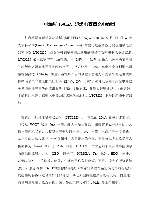
可编程150mA 超级电容器充电器具加利福尼亚州米尔皮塔斯(MILPITAS, CA) – 2008 年 6 月17 日– 凌力尔特公司(Linear Technology Corporation) 推出无电感器型可编程超级电容器充电器LTC3225,该器件可满足便携式应用的高峰值功率和电池备份需求。
LTC3225 采用低噪声充电泵架构,用2.8V 至5.5V 的输入电源将两节串联的超级电容器充电至固定输出电压(4.8V/5.3V 可选)。
充电电流可利用电阻编程至高达150mA,而且该器件具有自动容量平衡能力,无需平衡电阻就可保持两节电容器上的电压相等(2.4V/2.65V 可选)。
这可以使每个超级电容器免遭因电池容量失配或泄漏所引起的过压损坏,并最大限度地减少了电容器上的耗用电流。
在输入电源去除或短路到地时,LTC3225 不会让超级电容器放电。
在输出电压处于稳定状态时,LTC3225 以非常低的20uA 静态电流工作,且仅从VOUT 吸取2uA 电流。
输入电源去除后,随着该集成电路自动进入低电流停机状态、从超级电容器吸取不到1uA 电流,电流将进一步降低。
基本充电电路仅需 3 个外部组件,占用很小的空间,而且该集成电路采用占板面积为6mm2 的纤巧DFN 封装。
LTC3225 非常适用于具有高峰值功率负载的限流应用,如LED 闪光灯PCMCIA Tx 脉冲、HDD 脉冲、GPRS/GSM 传输等。
此外,它还可用作备份电源。
而且,较大的板级系统(例如:服务器和RAID/海量存储器系统) 常常还需要简洁的高功率后备电源,而超级电容器很适合用作这种电源。
其它关键特点包括自动再充电、内置限流和热量限制、以及有助于减小外部组件尺寸的1MHz 高工作频率。
- 1、下载文档前请自行甄别文档内容的完整性,平台不提供额外的编辑、内容补充、找答案等附加服务。
- 2、"仅部分预览"的文档,不可在线预览部分如存在完整性等问题,可反馈申请退款(可完整预览的文档不适用该条件!)。
- 3、如文档侵犯您的权益,请联系客服反馈,我们会尽快为您处理(人工客服工作时间:9:00-18:30)。
电子报/2009年/8月/2日/第016版
电子文摘
超级电容充电IC——LTC3225及应用
青化编译
超级电容又被称为电气双层电容(EDLC),其电容量从1F~1000F,是新型的短期蓄电设备。
对于电车或电梯在制动时产生的电力,可用大容量的超级电容来蓄电,达到能源的再生;而对于小功率的太阳能电池,则可用小容量的超级电容来蓄电。
对超级电容的充电,要求具有过充电保护的功能。
因为超级电容的额定电压一般为2.5V左右,也有2.75V和3.0V的产品;但额定电压为5.0V的产品。
其内部则是由两只2.5V电容串联构成的。
最近也有了锂离子超级电容(LIC),其额定电压可达 3.8V~4.0V。
但它被规定有使用下限电压。
超级电容耐压越高。
所蓄能量也越大。
能量U=1/2C×V2。
另外,由于超级电容的内阻比电池内阻低得多,故初始电流很大。
所以要用恒压恒流电源给超级电容充电。
LTC3225是专为两只串联的2.5V超级电容充电而设计的集成电路,输出电压4.8V~5.3V。
它根据分别对两只电容端电压的监测来工作,电压低时自动开始充电,充满自停。
故不适用于无中心抽头的串联型超级电容充电;也不适用于有下限电压限制的锂离子超级电容。
LTC3225利用内部的电荷泵来充电,即使两只串联的超级电容的容量有误差,电荷泵也可保证对其平衡充电。
如图1所示,在LTC3225外部接有快速电容,电荷泵首先对快速电容充电,一旦充满,快速电容上的电荷就向超级电容转移。
充电过程是以一定间隔在充电和电荷转移间进行,且是按串联超级电容的顺序逐一转移的。
所以,可以得到比输入电压高的充电电压,即使输入电压仅2.8V,也可对串联后达5.5V的超级电容充电。
如果用普通的恒压恒流电源给串联的超级电容充电,必须给每只超级电容并联电压平衡电路(图2),但LTC3225利用电荷泵来平衡两个串联超级电容的电压,就不必再加平衡电路。
PGOOD端子用于监视充电状况,当未充满电时,该端子为“L”电平。
SHDN端子为“L”电平时,芯片停止工作。
充电停止;Cout、Cx端子呈高阻抗,超级电容上的电荷不会经上述端子泄漏。
在未充电的场合。
上述端子仅有不到1μA的泄漏电流。
LTC3225为双列10脚贴片封装。
充电电流150mA,几乎没有外围元件即可构成微小体积的充电电路,适用于电子设备中对付瞬时低电压的后备电源。
瞬时补偿:当正在工作的电子设备突遇电源电压瞬时跌落时,超级电容即时放电,保证设备正常工作。
此时在电源部分应加入肖特基快恢复二极管作隔离,如图3。
关机后的散热:在关闭电子设备的电源后。
超级电容放电,维持散热风扇继续工作一段时间,散去余热。