Switching Volt Transient Prot Schemes For High Curr Igbt Modules
电镀专业术语中英文对照

电镀专业术语中英文对照1 大气暴露试验atmospheric corrosion test2 中性盐雾试验(NSS试验) neutral salt spray test(NSS—test)3 不连续水膜water break4 pH计pH meter5 孔隙率porosity6 内应力internal stress7 电导仪conductivity gauge8 库仑计(电量计)coulomb meter9 旋转圆盘电极rotating disk electrode10 旋转环盘电极rotating ring disk electrode11 针孔pores12 铜加速盐雾试验(CASS试验) copper accelerated salt spray (CASS test ).13 参比电极reference electrode14 甘汞电极calomel electrode15 可焊性solder ability16 硬度hardness17 金属变色tarnish18 点滴腐蚀试验dropping corrosion test19 玻璃电极glass electode20 结合力adhesion21 哈林槽Haring cell22 恒电势法potentiostatic method23 恒电流法galvanostatic method24 交流电流法a。
c method25 树枝状结晶trees26 脆性brittleness27 起皮peeling28 起泡blister29 剥离力试验机spalling30 桔皮orange peel简单的电镀术语—中英对照镀(Plating)电镀(Electroplating)自催化镀(Auto-catalytic Plating)化学镀(Chemical Plating)无电镀(Electroless Plating)浸渍镀(Immersion Plating)阳极氧化(Anodizing)化学转化层(Chemical Conversion Coating)钢铁发蓝(Blackening),俗称”发黑“钢铁磷化(Phosphating)铬酸盐处理(Chromating)金属染色(Metal Colouring)涂装(Paint Finishing),包括各种涂装如手工涂装、静电涂装、电泳涂装等热浸镀(Hot dip)热浸镀锌(Galvanizing),俗称"铅水"热浸镀锡(Tinning)PVD 物理气相沈积法(Physical Vapor Deposition)真空镀(Vacuum Plating)离子镀(Ion Plating)CVD 化学气相沈积法(Chemical Vapor Deposition)电镀术语解释及英文名称ABS塑料电镀plastic plating processpH计pH meter 测定溶液pH值的仪器.螯合剂chelating agent 能与金属离子形成螯合物的物质。
高速切换半导体控制器使用说明说明书
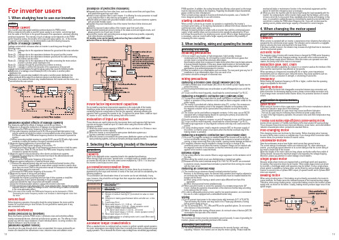
1. When studying how to use our invertersNotesLeakage currentThis inverter uses high-speed switching semiconductors for PWM control.When a relatively long cable is used for power supply to an inverter, current may leak from the cable or the motor to the ground because of its capacitance, adversely affecting peripheral equipment. The intensity of such a leakage current depends on the PWM carrier frequency setting, the lengths of the input and output cables, etc., of the inverter. To prevent current leakage, it is recommended to take the following measures. [Effects of leakage current]Leakage current which increases when an inverter is used may pass through the following routes:Route (1) ... L eakage due to the capacitance between the ground and the noise reduction fi lterRoute (2) ... L eakage due to the capacitance between the ground and the inverterRoute (3) ... L eakage due to the capacitance between ground and the cable connecting the inverter and the motorRoute (4) ... L eakage due to the capacitance of the cable connecting the motor and an inverter in another power distribution lineRoute (5) ... L eakage through the grounding line common to motorsRoute (6) ... L eakage to another line because of the capacitance of the groundLeakage current which passes through the above routes may cause the following trouble.l M alfunction of a leakage circuit breaker(ELCB) in the same or another power distribution linel M alfunction of a ground-relay installed in the same or another power distribution linel N oise produced at the output of an electronic device in another power distribution linel A ctivation of an external thermal relay installed between the inverter and the motor, at acurrent below the rate current[Measures against effects of leakage current]The measures against the effects of leakage current are as follows:1) Measures to prevent the malfunction of leakage circuit breakers(ELCB)(1) Decrease the PWM carrier frequency of the inverter. Note)(2) Use radio-frequency interference-proof ELCBs as ground-fault interrupters in notonly the system into which the inverter is incorporated but also other systems. When ELCBs are used, the PWM carrier frequency needs to be increased to operate the inverter.(3) When connecting multiple inverters to a single ELCB, use an ELCB with a high currentsensitivity or reduce the number of inverters connected to the ELCB.2) Measures against malfunction of ground-fault relay:(1) Decrease the PWM carrier frequency of the inverter. Note)(2) Install ground-fault relays with a high-frequency protective function in both the sameand other lines. When ELCBs are used, the PWM carrier frequency needs to beincreased to operate the inverter.3) Measures against noise produced by other electric and electronic systems:(1) Separate the grounding line of the inverter from that of the affected electric andelectronic systems.(2) Decrease the PWM carrier frequency of the inverter. Note)4) Measures against malfunction of external thermal relays:(1) Remove the external thermal relay and use the electronic thermal function of theinverter instead of it. (Unapplicable to cases where a single inverter is used to drive more than one motor. Refer to the instruction manual for measures to be taken when thermal relays cannot be removed.)(2) Decrease the PWM carrier frequency of the inverter. Note)5) Measures by means of wiring and grounding(1) Use a grounding wire as large as possible.(2) Separate the inverter's grounding wire from that of other systems or install thegrounding wire of each system separately to the grounding point.(3) Ground (shield) the main circuit wires with metallic conduits.(4) Use the shortest possible cables to connect the inverter to the motor.(5) If the inverter has a high-attenuation EMC noise reduction fi lter, change the groundingcapacitor switch to reduce the leakage current. Note that doing so leads to a reduction in the noise attenuating effect.Note) I n the case of this inverter, the PWM carrier frequency can be decreased to 2.0kHz.Decreasing the carrier frequency results in an increase in electromagnetic noise from the motor.Ground faultBefore beginning operation, thoroughly check the wiring between the motor and the inverter for incorrect wiring or short circuits. Do not ground the neutral point of anystar-connected motor.Radio interference[Noise produced by inverters]Since this inverter performs PWM control, it produces noise and sometimes affects nearby instrumental devices, electrical and electronic systems, etc. The effects of noise greatly vary with the noise resistance of each individual device, its wiring condition, the distance between it and the inverter, etc.[Measures against noises]According to the route through which noise is transmitted, the noises produced by an inverter are classifi ed into transmission noise, induction noise and radiation noise.PWM waveform. In addition, the cooling becomes less effective at low speed, so the torquemust be reduced according to the frequency. Regarding the allowable torque characteristic,please confi rm its motor manufacturer.When constant-torque operation must be performed at low speeds, use a Toshiba VFmotor designed specifi cally for use with inverters.Starting characteristicsWhen a motor is driven by an inverter, its operation is restricted by the inverter’soverload current rating, so the starting characteristic is different from those obtained fromcommercial power supply operation.Although the starting torque is smaller with an inverter than with the commercial powersupply, a high starting torque can be produced at low speeds by adjusting the V/f pat-tern torque boost amount or by employing vector control. When a larger starting torqueis necessary, select an inverter with a larger capacity and examine the possibility ofincreasing the motor capacity.3. When installing, wiring and operating the inverterInstalling and wiringInstalling precautions(1) D o not install in any location of high temperature, high humidity, moisturecondensation and freezing. Do not install the inverter where there are gases thatcorrode metal or solvents that adversely affect plastic.Avoid locations where there is exposure to water and/or where there may be large amountsof dust and metallic fragments. In this case, please install inverters in the enclosure typecabinet. The cabinet must be considered its size and the cooling method to allow thespecifi cations of an ambient temperature for inverters.(2) M ust be installed in non-infl ammables such as metals. The rear panel gets very hot. Ifinstallation is in an infl ammable object, this can result in fi re.(3) I nverters should be arranged in horizontal rows.Wiring precautionsInstalling a molded-case circuit breaker [MCCB](1) I nstall a molded-case circuit breaker (MCCB) on the inverter's power supply input toprotect the wiring.(2) A void turning the molded-case circuit breaker on and off frequently to turn on/off themotor.(3) T o turn on/off the motor frequently, close/break the control terminals F (or R)-CC.Installing a magnetic contactor [MC] [primary side](1) T o prevent an automatic restart after the power interruption or overload relay hastripped, or actuation of the protective circuit, install an electro-magnetic contact in thepower supply.(2) T he inverter is provided with a failure detection relay (FL), so that, if its contacts areconnected to the operation circuit of the magnetic contactor on the primary side,the magnetic contactor will be opened when the protective circuit of the inverter isactivated.(3) T he inverter can be used without a magnetic contactor. In this case, use an MCCB(equipped with a voltage tripping device) for opening the primary circuit when theinverter protective circuit is activated.(4) A void turning the magnetic contactor on and off frequently to turn on/off the motor.(5) T o turn on/off the motor frequently, close/break the control terminals F (or R)-CC.(6) I nstall surge suppressor on any magnetic contactor and relay coils used around theinverter.(7) I f using a braking resistor, install a magnetic contactor (MC) to the power supply ofthe inverter, so that the power circuit opens when the internal overload relay of thebraking resistor is activated.Installing a magnetic contactor [MC] [secondary side](1) A s a rule, if a magnetic contactor is installed between the inverter and the motor, donot turn on/off while running. (If the secondary-side contactor is turned on/off whilerunning, a large current may fl ow in the inverter, causing inverter damage and failure.)(2) A magnetic contactor may be installed to change the motor or change to thecommercial power source when the inverter is stopped. Always use an interlock withthe magnetic contactor in this situation so that the commercial power supply is notapplied to the inverter's output terminals.External signal(1) U se a relay rated for low currents. Mount a surge suppressor on the excitation coil ofthe relay.(2) W hen wiring the control circuit, use shielded wires or twisted pair cables.(3) B ecause all of the control terminals except FLA, FLB ,FLC,RY and RC are connectedto electronic circuits, insulate these terminals to prevent them from coming into contactwith the main circuit.Installing an overload relay(1) T his inverter has an electronic-thermal overload protective function.H owever, in the following cases, the thermal relay operation level must be adjusted oran overload relay matching the motor's characteristics must be installed between theinverter and the motor.(a) W hen using a motor having a rated current value different from that of theequivalent.(b) W hen driving several motors simultaneously.(2) W hen using the inverter to control the operation of a constant-torque motor (VFmotor), change the protective characteristic of the electronic thermal relay accordingto the setting of the VF motor.(3) I n order to adequately protect a motor used for low-speed operation, we recommendthe use of a motor equipped with a embedded thermal relay.Wiring(1) D o not connect input power to the output (motor side) terminals (U/T1,V/T2,W/T3).That will destroy the inverter and may result in fi re. Please pay attentions of wiringbefore power supply turns-on.(2) T he DC terminals (PA/+, PC/-,PBe and PB) are for specifi ed options. Do not connectother devices to these terminals.(3) W ithin 15 minutes after turning off input power, do not touch wires of devices (MCCB)connected to the input side of the inverter.GroundingThe inverters and motors must be connected to ground securely. In case of grounding forinverters, please use the grounding terminal of the inverter.Operating precautions(1) T he inverter operates in abnormal circumstances the security function, and stopsoutputting. However, the inverters can not stop the motors quickly. Please install the[Examples of protective measures]l S eparate the power line from other lines, such as weak-current lines and signal lines,and install them apart from each other.l I nstall a noise reduction fi lter in each inverter. It is effective for noise prevention to installnoise reduction fi lter in other devices and systems, as well.l S hield cables and wires with grounded metallic conduits, and cover electronic systemswith grounded metallic cases.l S eparate the power distribution line of the inverter from that of other devices andsystems.l I nstall the input and output cables of the inverter apart from each other.l U se shielded twisted pair wires for wiring of the weak-current and signal circuits, andalways ground one of each pair of wires.l G round the inverter with grounding wires as large and short as possible, separatelyfrom other devices and systems.All models, noise can be greatly reduced as they have a built-in EMC noisereduction filter on their input side.Power factor improvement capacitorsDo not install a power factor improvement capacitors on the output side of the inverter.Installing a power factor improvement capacitor on the output side causes currentcontaining harmonic components to fl ow into the capacitor, adversely affecting thecapacitor itself or causing the inverter to trip. To improve the power factor, install an inputAC reactor or a DC reactor on the primary side of the inverter.Installation of input AC rectorsThese devices are used to improve the input power factor and suppress high harmoniccurrents and surges. Install an input AC reactor when using this inverter under thefollowing conditions:(1) W hen the power source capacity is 500kVA or more, and when it is 10 times or moregreater than the inverter capacity.(2) W hen the inverter is connected the same power distribution system as athyristor-committed control equipment.(3) W hen the inverter is connected to the same power distribution system as that of distortedwave-producing systems, such as arc furnaces and large-capacity inverters.2. Selecting the Capacity (model) of the InverterSelectionCapacityRefer to the applicable motor capacities listed in the standard specifi cations.When driving a high-pole motor, special motor, or multiple motors in parallel, select suchan inverter that the sum of the motor rated current multiplied by 1.05 to 1.1 is less thanthe inverter's rated output current value.Acceleration/deceleration timesThe actual acceleration and deceleration times of a motor driven by an inverter aredetermined by the torque and moment of inertia of the load, and can be calculated by thefollowing equations.The acceleration and deceleration times of an inverter can be set individually. In anycase, however, they should be set longer than their respective values determined by thefollowing equations.Allowable torque characteristicsWhen a standard motor is combined with an inverter to perform variable speed operation,the motor temperature rises slightly higher than it normally does during commercial powersupply operation. This is because the inverter output voltage has a sinusoidal (approximate)mechanical brake or maintenance function in the mechanical equipment and thedevice for which the emergency stop is necessary.(2) W hen you drive the machine and the device that hangs the load repeatedly with theinverter, the semiconductor within inverter might cause thermal fatigue, and it cometo have a short life if a big current fl ows repeatedly when driving and stopping. In thiscase, it is possible to extend life span by controlling the starting current and the loadcurrent low or setting the PWM career frequency low. If you can not decrease thestarting current, please select larger capacity of inverters for current margins.4. When changing the motor speedApplication to standard motorsVibrationWhen a motor is operated with an inverter, it experiences more vibrations than when it isoperated by the commercial power supply. The vibration can be reduced to a negligiblelevel by securing the motor and machine to the base fi rmly.If the base is weak, however, the vibration may increase at a light load due to resonancewith the mechanical systemAcoustic noiseThe magnetic noise of motors with inverter drives is changed by PWM carrier frequency.In case of high PWM carrier frequency settings, its acoustic noise is almost same ascommercial power supply drives. Moreover, when the motors are operated over ratedrotation, the windy noise of the motors is increased.Reduction gear, belt, chainNote that the lubrication capability of a reducer or a converter used as the interface of themotor and the load machine may affected at low speeds.When operating at a frequencies exceeding 60 Hz or higher, power transmissionmechanisms such as reduction gear, belts and chains, may cause problems such asproduction of noise, a reduction in strength, or shortening of service life.FrequencyBefore setting the maximum frequency to 60 Hz or higher, confi rm that this operatingrange is acceptable for the motor.Starting methodWhen you drive the motor with changeable connection between star-connection anddelta-connection for decreasing starting current, please connect delta-connection only.If you change motor connection while inverter drives, the protective function of inverteroccurs.Application to special motorsGear motorWhen using an inverter to drive a gear motor, inquire of the motor manufacturer about itscontinuous operation range due to the followings:- The low-speed operation of a gear motor may cause insuffi cient lubrication- The loss of a gear may be increasing than commercial power supply drives.- I n case of the high frequency operation, the acoustic noise and motor temperature maybe higher.Toshiba Gold Motor (High-effi ciency power-saving motor)Inverter-driven operation of Toshiba Gold Motors is the best solution for saving energy.This is because these motors have improved effi ciency, power factor, and noise/vibrationreduction characteristics when compared to standard motors.Pole-changing motorPole-changing motors can be driven by this inverter. Before changing poles, however,be sure to let the motor come to a complete stop. If you change motor connection whileinverter drives, the protective function of inverter occurs.Underwater motorsNote that underwater motors have higher rated current than general motorsThe current ratings of underwater motors are relatively high. So, when selecting aninverter, you must pay special attention to its current rating so that the current rating ofthe motor is below that of the inverter.When the lengths of the motor cable are long, please use thicker cable than a table of‘Wiring devices’ because the maximum torque is decreased by the voltage dropping..Moreover, please pay attention to select leakage circuit breakers.Single-phase motorBecause single-phase motors are equipped with a centrifugal switch and capacitorsfor starting, they cannot be driven by an inverter. When single phase motors are drivenby inverters, a centrifugal switch and capacitors may be broken. If only a single-phase,power system is available a 3-phase motor can be driven by using a single-phase inputinverter to convert it into a 3-phase 200V output. (A special inverter and a 3-phase 200Vmotor are required.)Braking motorWhen using a braking motor, if the braking circuit is directly connected to the inverter'soutput terminals, the brake cannot be released because of the lowered starting voltage.Therefore, when using a braking motor, connect the braking circuit to the inverter's powersupply side, as shown on the below. Usually, braking motors produce larger noise in lowspeed ranges.For inverter users1819。
太赫兹材料与器件英文

太赫兹材料与器件英文With the rapid development of science and technology, the demand for high-speed communication and advanced imaging systems has increased in recent years. One of the most promising solutions for these needs is the use of Terahertz (THz) materials and devices.THz waves refer to electromagnetic radiation with frequencies between 0.1 and 10 THz. This frequency range is also known as the THz gap, which is an area in the electromagnetic spectrum that is difficult to access with traditional technologies. With the development of THz technology, it is possible to exploit THz waves for a range of applications, including imaging, sensing, communication, and security.To harness the potential of THz waves, researchers have focused on developing THz materials and devices. These materials and devices have unique properties that make them ideal for THz applications. For example, THz waves can pass through a range of materials, including plastics, wood, and clothing, making them ideal for security applications. THz devices can also detect subtle changes in materials, making them useful for medical imaging and quality control in manufacturing.The development of THz materials and devices has been facilitated by advances in nanotechnology, which allows the creation of new materials with controlled properties. One such material is graphene, which has extraordinary electron transport properties that make it ideal for THz applications.Other materials used for THz devices and components include gallium arsenide (GaAs), indium antimonide (InSb), and indium phosphide (InP).Apart from materials, THz devices also require components such as antennas, sources, and detectors. Antennas are used to generate and receive THz waves, while sources provide the energy required for THz radiation. Detectors, on the other hand, capture and convert the THz radiation into a form that can be analyzed.In summary, THz technology is a promising area of research that has already shown its potential in a range of applications. The development of THz materials and devices is essential to harnessing the potential of THz waves. Nanotechnology has enabled the creation of new materials with controlled properties, while components such as antennas, sources, and detectors are required for THz devices. With continued research and development, THz technology will undoubtedly lead to significant advances in communication, imaging, and sensing.。
真空有载分接开关在高压直流换流变压器中的运用

2011年第5卷第1期南方电网技术高压直流输电2011,V ol. 5,No. 1 SOUTHERN POWER SYSTEM TECHNOLOGY HVDCTransmission 文章编号:1674-0629(2011)01-0025-04 中图分类号:TM564;TM41 文献标志码:A真空有载分接开关在高压直流换流变压器中的运用沈大中,Axel Kraemer,Dieter Dohnal(德国MR公司,Falkensteinstr. 8, 93059 Regensburg, Germany)摘要:有载分接开关(on-load tap-changers,OLTC)是高压直流输电线路中现代换流变压器不可或缺的设备,可对系统的电压变化进行补偿,优化变频器控制角,并使高压直流系统降压运行成为可能。
但开关操作时产生的电流具有陡峭的非正弦波形,不仅增加了开关切换的负荷,也增加了开关的容量和尺寸,而且开关频繁操作对维护提出了很高的要求。
比较了换流变压器和电力变压器OLTC的操作条件。
真空开关技术的引入使得真空OLTC除了可以消除油的污染外,还具备独特的优势,可承受高切换负荷,可用在高压直流换流变压器上,OLTC的容量配置可以优化调整等。
真空OLTC免维护的操作次数可高达600 000次,维护工作可降至最低限度,大幅提升了换流变压器的可靠性和可用率。
通过优化OLTC额定容量可以节省开关的体积和重量,有助于开发超高压直流换流变压器。
关键词:有载分接开关;真空开关管;真空断流器;高压直流;变压器;换流变压器Application of Vacuum On-Load Tap-Changers in HVDC Converter TransformersSHEN Dazhong, Axel Kraemer,Dieter Dohnal(Maschinenfabrik Reinhausen GmbH, Falkensteinstr. 8, 93059 Regensburg, Germany)Abstract: On-load tap-changers (OLTCs) are indispensable components in modern converter transformers for HVDC transmissionlines. They compensate the system voltage variation, optimize the control angle of converter valves and realize the operation withreduced DC voltage. But the non-sinusoidal current waveshape with the high rate of rise during tap-change operation augments theswitching duties and leads to an over sizing of the OLTC, and the frequent tap-change operations result in high maintenance demand.The switching condition of OLTCs in converter transformers is compared to that of power transformers in this paper. The introductionof vacuum switching technology in OLTCs provides, besides the elimination of oil contamination, the unique advantage for heavyswitching duties as that in converter transformers for HVDC applications. The rating of the OLTC can be adjusted optimally to theservice duties. Since this new OLTC technique is maintenance-free up to 300,000 operations, the maintenance work can be reduced toa minimum. The reliability and the availability of converter transformers are therefore considerably improved. The sparing in volumeand weight through the optimized rating of OLTCs makes a contribution to the future effort in ultra HVDC development.Key words: on-load tap-changer; vacuum switching; vaccum interrupter; HVDC; transformer; converter transformer有载分接开关是高压直流系统中很重要的设备,可以改变绕组的匝数比,补偿电网电压的变化,根据系统功率因素,对控制角进行优化。
有关电镀的英语词汇

1 大气暴露试验atmospheric corrosion test2 中性盐雾试验(NSS试验) neutral salt spray test(NSS-test)3 不连续水膜water break4 pH计pH meter5 孔隙率porosity6 内应力internal stress7 电导仪conductivity gauge8 库仑计(电量计) coulomb meter9 旋转圆盘电极rotating disk electrode10 旋转环盘电极rotating ring disk electrode11 针孔pores12 铜加速盐雾试验(CASS试验) copper accelerated salt spray (CASS test ).13 参比电极reference electrode14 甘汞电极calomel electrode15 可焊性solder ability16 硬度hardness17 金属变色tarnish18 点滴腐蚀试验dropping corrosion test19 玻璃电极glass electode20 结合力adhesion21 哈林槽Haring cell22 恒电势法potentiostatic method23 恒电流法galvanostatic method24 交流电流法a.c method25 树枝状结晶trees26 脆性brittleness27 起皮peeling28 起泡blister29 剥离spalling30 桔皮orange peel简单的电镀术语-中英对照/article/428110.html镀(Plating)电镀(Electroplating)自催化镀(Auto-catalytic Plating)化学镀(Chemical Plating)无电镀(Electroless Plating)浸渍镀(Immersion Plating)阳极氧化(Anodizing)化学转化层(Chemical Conversion Coating)钢铁发蓝(Blackening),俗称”发黑“钢铁磷化(Phosphating)铬酸盐处理(Chromating)金属染色(Metal Colouring)涂装(Paint Finishing),包括各种涂装如手工涂装、静电涂装、电泳涂装等热浸镀(Hot dip)热浸镀锌(Galvanizing),俗称"铅水"热浸镀锡(Tinning)PVD 物理气相沈积法(Physical Vapor Deposition)真空镀(Vacuum Plating)离子镀(Ion Plating)CVD 化学气相沈积法(Chemical Vapor Deposition)电镀术语解释及英文名称/article/3897/art_information.htmlABS塑料电镀plastic plating processpH计pH meter 测定溶液pH值的仪器。
电机试验语汇中英文对照

第一部分:电机名称电机 electric machine交流电机 alternating-current machine直流电机 direct-current machine电动机 motor发电机 generator三相异步电机 three-phase induction motor 单相异步电机 single-phase induction motor 罩极式电机 shaded-pole motor同步电动机 synchronous motor并励电动机 shunt DC motor复励电动机 compound DC motor他励电动机 separately excited motor伺服电动机 servomotor控制电动机 control motor同步发电机 synchronous generator汽轮发电机 turboalternator水轮发电机 water-wheel generator自励发电机 self-excited generator并励发电机 shunt DC generator串励发电机 seriers field generator复励发电机 compound DC generator他励发电机 separately excited generator 测速发电机 tachometer generator励磁机 exciter永磁发电机 permanent magnet generator 异步发电机 asynchronous generator变速电动机 varying speed generator多速电动机 multi-speed generator调速电动机 adjustable-speed motor磁阻电动机 reluctance motor锥形转子电机 conical rotor machine电容电动机 capacitor motor无刷电机 brussless electric machine第二部分:电机部件机座 frame,stator frame底脚 foot接线盒 terminal box接线板 terminal board接线柱 terminal column端盖 endshield 凸缘端盖 flange endshield吊环 eyebolt铭牌 data plate,name plate定子 stator定子铁心 stator core转子 rotor转子铁心 rotor core定子槽 stator slot转子槽 rotor slot槽楔 slot wedge槽绝缘 slot liner相间绝缘 phase coil insulation(线圈绝缘)层间绝缘 coil side separator绕组 winding定子绕组 stator winding转子绕组 rotor winding散嵌绕组 random winding成形绕组 performed winding同心式绕组 concentric winding交叉式绕组 cross winding叠绕组lap winding波绕组 wave winding蛙式绕组 frog-leg winding单层绕组 single layer winding双层绕组 two-layer winding单-双层绕组 single and two-layer winding 正弦绕组 sine winding长距绕组 long pitch winding短距绕组 short pitch winding电枢 armature电枢绕组 armature winding励磁绕组 field winding他励绕组 separately field winding串励绕组 series field winding并励绕组 shunt field winding换向绕组 commutating winding补偿绕组 compensation winding主绕组 primary winding辅绕组 secondary winding磁极 pole极靴 pole shoe鼠笼式转子 squirrel-cage rotor绕线式转子 wound rotor凸极转子 salient poles rotor隐极转子 nonsalient poles rotor 铸铝转子 casting aluminium rotor 铜条转子 copper bar rotor永磁转子 permanent magnet rotor 锥形转子 conical rotor轴 shaft轴伸shaft extension键槽 keyway,key seat键 key轴承 bearing滚动轴承 ball bearing滑动轴承 sliding bearing风扇 fan风扇罩 fan cover,fan housing 鼓风机 air pump进风孔(口) air inlet出风孔(口) air outlet换向器 commutator集电环 collector ring电刷(碳刷) carbon brush电刷架 brush rocker电刷压簧 brush pressure spring刷盒 brush box离心开关 centrifugal switch第三部分电机技术参数型号 type,model额定功率 rated power额定电压 rated voltage额定频率 rated frequency额定电流 rated current转子电压 rotor voltage转子电流 rotor current励磁方式 field manner他励 separately excited并励 shunt field串励 series field复励 compound field自励 self-excited单相 single phase三相 three phase同步转速 synchronous speed 额定转速 rated speed最高转速 maximum speed工作制 duty防护等级 degree of protection冷却方式 cooling method重量 weight绝缘等级 insulation class接线方式 mode of connection接线图 connection diagram星形连接 star connection三角形连接 delta connection安装方式 mounting type第四部分电机性能参数绝缘电阻 insulation resistance温升 temperature rise效率 efficiency功率因数 power factor转差率 slip起动转矩 start torque起动电流 start current最大转矩 maximum torque最小转矩 minimum torque牵入转矩 pull-in torque失步转矩 pull-out torque电磁转矩 electromagnetic torque 空载电流 no load current空载损耗 no load loss机械损耗 machine loss铁损耗 core loss定子铜耗 stator copper loss转子铜耗 rotor copper loss励磁铜耗 field loss电刷损耗 carbon brush loss杂散损耗 stray loss仪表损耗 meter loss总损耗 total loss输入功率 input power输出功率 output power视在功率 apparent power无功功率 reactive power直流电阻 DC resistance过电压 over voltage过电流 over current过转矩 over torque耐电压 voltage-withstand匝间耐电压 interturn voltage-withsatnd超速 over speed噪声(声压级) noise(LP)噪声(功率级) noise(LW)振动(速度) vibration severity换向火花 commutation spark转速差 speed difference转速调速率 speed regulation电压调速率 voltage regulation正弦畸变率 voltage sine-wave distortion factor电话谐波因数telephone harmonics factor谐波电压因数harmonics voltage factor第五部分试验设备及仪器仪表变压器 transformer调压器 voltage regulator开关柜 switch disc控制台 control gear试验台 test bed仪表 instrument,meter万用表 universal meter瓦特表 wattmeter电流表 ammeter电压表 voltmeter电磁式仪表 electromagnetic instrument电动式仪表 electrodynamic instrument磁电式仪表 magnetoelectric instrument整流式仪表 rectifier instrument转速表 speedometer兆欧表 meg meter频率表 frequency instrument声级表 noise meter测振表 vibration measurement测力计 dynamometer温度计 thermometer测功机 dynamometer示波器 oscillograph电阻器 resistor 电感器 inductor电容器 capacitor整流器 rectifier逆变器 inventor变频器 frequency convertor变频机 frequency changer传感器 sensor打印机 printer绘图机 drafting machine第六部分电工学术语电流 current电流密度 current density电压 voltage电位 electric potential电位差 electric potential difference 电动势 electromotive force感应电动势 inducted EMF电阻 resistance电阻性电路 resistance circuit电阻率 resistivity电导 conductance电导率 conductivity电容 capacitor电容性电路 capacitive circuit电感 inductance电感性电路 inductive circuit阻抗 impedance容抗 capacitive reactance感抗 inductive reactance功率 power有功功率 active power相位角 phase angle相序 phase sequence相量 phasor相量图 phasor diagram初相位 initial phase滞后 lag超前 lead磁场 magnetic field磁场强度 magnetizing force磁通 flux磁感应强度 flux density磁阻 reluctance磁导率 permeability磁动势 magnetomotive force磁化 magnetization磁滞 hysteresis磁滞回线 hysteresis loop磁滞损耗 hysteresis loss磁化曲线 magnetization curve磁极 pole漏磁通 leakage flux回路 loop导体 conductor导纳 admittance电路 circuit开路 open circuit短路 short circuit串联 series connection并联 parallel connection直流 direcit current正极 positive pole负极 negative pole交流电 alternating current正弦交流电 sinusoidal current三相 three phases三相对称电路symmetrical three-phase circuit 三相三线制 three-phase three-wire system 三相四线制 three-phase four-wire system 中点 neutral point中线 neutral conductor接地 put to earth基波(分量) fundamental(component)谐波(分量) harmonics(component)瞬时值 instantaneous value平均值 mean value均平方根值 R.M.S(effective)value周期 period频率 frequency峰值,振幅 peak value双倍振幅 form factor of a symmetricalalternating quantity谐振,共振 resonance三相的不平衡度degrees of unbalance in athree-phase system安培 Ampere 伏特 Volt瓦特 Watt欧姆 Ohm韦伯 Weber高斯 Gauss麦克斯韦 Maxwell特斯拉 Tesla库仑 Coulomb亨利 Henry法拉 Farad焦耳 Joule奥斯特 Oersted赫兹 Hertz欧姆定律 Ohm’s law焦耳定律 Joule’s law楞次定律 Lenz’s law全电流定律 law of total current基尔霍夫电流定律Kirchhoff’s current law(KCL)基尔霍夫电压定律Kirchhoff’s voltage law 法拉第电磁感应定律Farad’s electromagnetic induced law第七部分试验术语试验 test性能试验 performance tests型式试验 type tests检查试验 routine tests抽样试验 sampling tests验收试验 acceptance tests效率的直接测定direct calculation of efficiency效率的间接测定 indirect calculation of efficiency效率的损耗分析 calculation of efficiencyfrom summation of losses对拖试验 mechanical back to back test回馈试验 electrical back to back test空载试验 no load test开路试验 open-circuit test稳态短路试验sustained short-circuit test突然短路试验 sudden short-circuit test零功率因数试验zero power factor test温升试验 temperature rise test波形测定 waveform measurement谐波试验 harmonic test堵转试验 locked-rotor test起动试验 starting test牵入转矩试验 pull-in test最大转矩测定 pull-out test,breakdown test换向试验 commutation test无火花换向试验black-hand test直流电阻测试 resistance test铁心损耗试验 core test超速试验 overspeed test振动试验 vibration test噪声级试验 noise-level test轴电压试验 shaft-voltage test转向试验 rotation test相序试验 phase-sequence test极性试验 polarity test换向片间电阻试验 har-to-test绝缘电阻试验 insulation resistance test耐电压试验 high-voltage test介质损耗角试验loss tangent test匝间试验 inerturn test,turn-to-turn test 饱和特性 saturation characteristic开路特性(空载特性) open-circuit characteristic(no load characteristic)负载特性 load characteristic短路特性 short-circuit characteristic堵转特性 locked-rotor characteristic零功率因数特性 zero power-factor characteristic电压调整特性 voltage regulation characteristic转速调整特性 speed regulation characteristicV型曲线特性V-curve characteristic功角特性 load angle characteristic外特性 external characteristic伏安特性 volt-ampere characteristic机械特性 torque-speed characteristic 调节特性 regulating characteristic磁化曲线 magnetization curve磁滞曲线 hysteresis curve 圆图 circle diagram环境温度 ambient temperature 冷态 cold state冷态电阻 cold resistance热态 thermal state热态电阻 thermal resistance 热稳定 thermal stabilization 环境噪声 ambient noise level 额定值 rated value定额 rating。
太阳能技术术语 中英文对照

太阳能技术术语中英文对照AAmpere的缩写,安培a-Si,amorphoussilicon的缩写,含氢的,非结晶性硅。
Absorption,吸收。
Absorptionofthephotons:光吸收;当能量大于禁带宽度的光子入射时,太阳电池内的电子能量从价带迁到导带,产生电子空穴对的作用,称为光吸收。
Absorptionscoefficient,吸收系数,吸收强度。
AC,交流电。
Ah,安培小时。
Acceptor,接收者,在半导体中可以接收一个电子。
alternatingcurrent,交流电,简称交流.一般指大小和方向随时间作周期性变化的电压或电流.它的最基本的形式是正弦电流.我国交流电供电的标准频率规定为50赫兹。
交流电随时间变化的形式可以是多种多样的。
不同变化形式的交流电其应用范围和产生的效果也是不同的。
以正弦交流电应用最为广泛,且其他非正弦交流电一般都可以经过数学处理后,化成为正弦交流电的迭加。
AM,airmass的缩写,空气质量。
的倍数来表示。
当大气压力P=1.013巴,天空无云时,海平面处的大气质量为1。
amorphoussiliconsolarcell:非晶硅太阳电池(asi太阳电池)用非晶硅材料及其合金制造的太阳电池称为非晶硅太阳电池,亦称无定形硅太阳电池,简称asi太阳电池。
Angleofinclination,倾斜角,即电池板和水平方向的夹角,0-90度之间。
Anode,阳极,正极。
BBackSurfaceField,缩写BSF,在晶体太阳能电池板背部附加的电子层,来提高电流值。
Bandbreak,在半导体中,价带和导带之间的空隙,对于半导体的吸收特性有重要意义。
Becquerel,Alexandre-Edmond,法国物理学家,在1839年发现了电池板效应。
BSF,backsurfacefield的缩写。
Bypas-Diode,与太阳能电池并联的二极管,当一个太阳能电池被挡住,其他太阳能电池产生的电流可以从它处通过。
外文翻译晶闸管的高能脉冲式开关特性

外文原文与译文High-Energy Pulse-SwitchingCharacteristics of ThyristorsAbstractExperiments were conducted to study the high energy, high dildt pulse-switching characteristics of SCR's with and without the amplifying gate. High dildt. high-energy single- shot experiments were first done. Devices without the amplifying gate performed much better than the devices with the amplifying gate. A physical model is presented to describe the role of the amplifying gate in the turn-on process, thereby explaining the differences in the switching characteristics. The turn-on area for the failure of the devices was theoretically estimated and correlated with observations. This allowed calculation of the current density required for failure. Since the failure of these devices under high dildt conditions was thermal in nature, a simulation using a finite-element method was performed to estimate the temperature rise in the devices. The results from this simulation showed that the temperature rise was significantly higher in the devices with the amplifying gate than in the devices without the amplifying gate. Fromthese results, the safe operating frequencies for all the devices under high dildt conditions was estimated. These estimates were confirmed by experimentally stressing the devices under high di/dt repetitive operation.I. INTRODUCTIONRecent innovations in semiconductor device designs and advances in manufacturing technologies have helped evolve high-power thyristors. These devices are designed to operate in a continuous mode for applications such as ac- to-dc power conversion and motor drives. Until recently, their application to high-power pulse switching was mostly unknown. One of the main reasons that has discouraged the use of thyristors for high-speed, high-energy switching is their low dildt rating. The limiting value of the dildt before damage occurs is related to the size of the initial turn-on area and the spreading velocity [I]. Recent experimental results presented in [2]-[4] show that with increased gate device, SCR's and GTO's having highly interdigitated gate-cathode structures can reliably operate under high dildt conditions on a single-shot basis. Previously, SCR's have also been used for repetitive switching of 1 kA, 10 ps wide pulses having a dildt of about 10 000 Alps, at 500 and 800 Hz for a 10 h period [SI. It is reported in [6] that GTO modules (five devices in series) can block kV and switch kA pulses having a dildt of 2500 A/ks at frequencies of 100 Hz. Asymmetric devices,such as the ASCR's in a stack assisted by saturable inductors, have shown the potential to repetitively switch high-current pulses with di/dt of about 2000 Alps, on the order of kilohertz [7].Under high dildt conditions the junction temperatures can vary rapidly in high-power devices (6C s) [8]. The failure of these devices under~10/these conditions is normally thermal in nature. It has been reported [9],that the temperature of destruction due to a tum-on dildt failure is in the range of1100~1300C, below the melting point of silicon (1415°C). The rise in average temperature is therefore completely inade- quate as a measure of device applicability for pulse-switching applications. Since a simple experimental technique is not available to measure the instantaneous temperature rise, the spatio-temporal distribution of temperatures in the devices has to be estimated using computer-aided techniques.In this paper, the high dildt single-shot experimental re- sults are given in brief. A qualitative physical model is then proposed to explain the experimental results, which are presented in detail elsewhere [3]. Next, the results from the thermal analysis using FEM, given in detail in [lo], are briefly presented. The particulars of the experimental arrangement for the repetitive testing of the devices, results from these experi- ments, and their correlation with the numerical predictions are given in the discussion.11. SINGLE-SHOT EXPERIMENTSInverter-grade SCR's with the amplifying gate (unshorted device) andwithout the amplifying gate (shorted device) were used for experimentalstudies to determine the role of the amplifying gate during the turn-onprocesses of the device. The SCR's used for the tests were symmetric withinvolute gate-cathode structures. They were rated for a forward andreverse blocking voltage of kV (at 25°C) and . kV (at 125°C). Theexperimental details and results are fully presented elsewhere [3]. Theexperimental arrangement and the results are given in brief below.The devices were electrically characterized initially and recharacterizedafter testing in a type E pulse-formingnetwork (PFN) that has a totalimpedance of 0. This network delivers a 15 kA, 10 ps wide pulse whencharged to a voltage of kV. The di/dt of this 15-kA pulse is 125000 μ. The gate trigger used for switching the SCR's was a 100 A, 500 ns /A strapezoidal current di/dt of the gate pulse was 980 /A sμ.The unshorted devices failed while switching a peak anode current ofkA at a dildt of about 26000 /A sμin a PFN charged to kV. Under thesame trigger conditions, the shorted devices successfully switched 13 kAat a dildt of 100000 /A sμ, in a PFN charged to 2 kV. A comparison of theperformance of the two types of devices is presented in Table I. Theampliyfing gate seems to inhibit the tum-on speed of the device. In theunshorted devices,which failed catastrophically, the region of failurearound the amplifying gate can be seen as a hot spot. All these results point to the fact that the conduction area near the amplifying gate region in the unshorted device is very small. This leads to an increase in current density in the device and, therefore, the instantaneous rise in temperature exceeds the threshold value for failure: about 1100°C [9].TABLE1SINGLE-SHOT EXPERIMENTAL RESUILSTSFig. 1. Typical A I (CH1) and AK V (CH2) switching waveforms of the unshorted device, CH1-1931 A/div, CH2-500 V/div, Timebase-100ns/div.111. ROLEOF THE AMPLIFYING GATEThe results presented in the previous section show that the deviceswithout the amplifying gate (shorted devices) better than the devices with the amplifying gate (unshorted devices). The typical switching waveforms of the unshorted and the shorted devices are shown in Figs. 1 and 2, respectively. In the case of the unshorted device, the anode current rises to a certain value and remains at that value for about ns before rising further its peak value (when the resistance of the device reduces as a result of more turned-on area). This behavior is not seen when the shorted device is used for switching. The anode current switched by the shorted devices has a smooth rising edge. The dynamic resistance of the two devices (computed from the V,Kand .Fig. 2. Typical A I (CH1) and AK V (CH2) and power loss(MULL) of the shorted device . CH1-3190 A/div, CH2-500 V/div, baser-100ns/div.Dynamic resistance of the device versus timeis shown in Fig. 3. From this plot it can be seen that the shorted device has a lower dynamicresistance compared to the unshorted device at every instant of time during the rise- time phase of the tum-on process. The results presented so far indicate that more device area is tumed on in the shorted device as compared to that in the unshorted device. It can be concluded that the amplifying gate is inhibiting the tum-on process under high di/dt switching conditions and is therefore to the performance Of the device. This be understood by 'Onsidering the tum-on sequences in the two types Of devices with the proposed given For this the cross-sectional views of the unshorted device and that Of the shorted device are shown in Figs. 4and 5,respectively.Fig. 4. Cross-sectional view of the unshorted deviceFig. 5. Cross-sectional view of the shorted deviceTurn-on Process in the Unshorted DeviceWhen the gate current (1) is injected into the p-base through the pilot gate contact (Fig. 4), electrons are injected intothe p-base by the n+ emitter with a certain emitter injection efficiency. These electrons traverse through the p-base (time taken for this process is called the transit time) and accumulate near the depletion region. This negative charge accumulation leads to injection of holes from the anode. At this time the device turns on after a certain delay, dictated by the P-base transit time [ll], and the pilot anode current (2) begins to flow through a small region near the pilot gate contact as shown in Fig. 4. This flow of pilot anode current corresponds to the initial sharp rise in the anode current waveform (phase I) shown in Fig. 1. The device then goes into phase 11, during which the anode current remains fairly constant,suggesting that the resistance of the region has reached its lower limit. This is because the pilot anode current (2) takes a finite time to traverse through the p-base laterally and become the gate current for the main cathode area. As a result, the n+ emitters start to inject electrons, which traverse the p-base vertically and after a certain finite time (transit time of the p-base) reach the region. The time taken by the above said processes is the reason for observing this characteristic phase The width Of the phase 'I is to the switching delay, suggesting that the p-base transit time is responsible. Once the main cathode region tums on, the resistance of the device decreases and the anode current begins to rise again (transition from phase I1 to phase 111). From here on the plasma-spreading velocity will dictate the rate at which the conduction area will increase. The dip in theFig. 6. Typical IC (CHI), (CH2) and power loss (MULT) of the unshorted device. C H I 4 0 A/div, CH2-20 V/div, MULT4096 W/div. Time base-100 ns/div.gate current (G I )and the increase in the gate-cathode voltage (GK V ),shown in Fig. 6,corresponds in time, to the pilot anode current flow. This supports the above suggestion that the anode current is initially forced to flow through a small area (high resistance) near the pilot-gate contact. Therefore the current density during phase I and phase I1 is very high and leads toa considerable increase in the local temperature.It was reported earlier in [9] that failure temperature of the device is about 1200°C. Based on this the conduction area and the current density for the failure of the device can be estimated as follows. fie adiabatic heat energy of dissipation in a volume can be mathematically related to the temperature rise in the volume as given below.()E MC T ρ=∆ (1)where E is the energy dissipated in the volume, M is the mass of the volume, C ρ is the heat capacity (specific heat at constant pressure) ofthe material, and AT is the temperature rise in the volume.Equation (1) can be modified as:()E VC T ρρ=∆ (2)where ρ is the mass density of the material and V is the volume of the material = area A ⨯ thickness h. Therefore, the conduction area for failure can be estimated as()E A C h T ρρ=∆ (3)Specific heat is a function of temperature, but Saturates at about 140°C. Since the failure temperature is 1000°C, the value of specific heat used for the calculation is its saturated value. The values for the properties of silicon used in the calculations are given below.302.3/0.8//g cm C J g C ρρ==The thickness of the device is approximately 500m μ. Using these values the computed area is 2mm .A photograph of the damaged unshorted device is shown in Fig. 7. The burnt spot is visible near the pilot-gate contact, and the width of the burnt spot is about 2 mm . Assuming the current was flowing in an annular region with this width, the area of current conduction was calculated to be 23.8mm .This agrees with the value computed in terms of the energy from (3). The current density in the device during phase I1 is then 921.8610/A m ⨯. This agrees with the value given in [ 121 for the failure of the device.Turn-on Process in the Shorted DeviceThe cross-sectional view of the shorted device (in which the ampliyfing gate was bypassed) is shown in Fig. S. When the gate current is injected, it flows laterally (l), and directly tums on part of the main cathode area, and the anode current (2) starts to flow. The current rise is therefore smooth (Fig. 2) and the phase II interval observed in the switching waveforms of the unshorted device is not seen here. The resistance of the device is continually decreasing as controlled by the plasma-spreading velocity. The dynamic resistance of the shorted device is lower compared to that of the unshorted device. The fact that phase II interval is not present in the switching waveforms of the shorted device causes less power loss in the device. This is further supported by the gate waveforms shown in Fig. 8, which are not distorted when the anode current begins to flow. Therefore the shorted devices are able to switch higher currents at very high di/dt values as compared to the unshorted devices. Finally, it can be concluded that the amplifying gate structure is detrimental to the device's performance if the rise time of the anode current is comparable to the p-base transit time.IV. TRANSIENTTHERMALANALYSISThe di/dt failure is caused by the instantaneous rise in temperature in the small conduction area obtained immediately after tum-on. Transient thermal analysis was performed inFig. 8. Typical IC (CHI), (CH2) and power loss (MULT) for the shorted device. C H 1 4 0 A/div, CH2--10 V/div, MULT-2048 W/div. Time base-I00 ns/div.order to estimate the temperature rise in the shorted and unshorted devices. A general-purpose FEM program called FIDAP' was employed for this analysis. The modeling pro- cedure and all the results are presented in detail in [lo]. A brief summary of this analysis is given below.The device and the mounting structure taking the symme- tries into account were modeled as the heat flow domain. This domain was represented by specifying the actual coordinates of the various regions in the domain. Depending on the temperature gradients expected in the various regions, the number of grids required for the analysis in order to obtain accurate results was decided. The properties of the various materials, namely, thermal conductivity, specific heat, andmass density, were specified. The initial conditions were specified to be 27°C for the entire domain. The symmetry boundaries were treated as insulating boundaries and were modeled by specifying the heat flux outflow to be zero. The other boundaries were maintained at 27°C. Since the experimental tests were on a single-shot basis, the nature of the problem had to be classified as transient. The current flow paths were different in the shorted and the unshorted devices, so different domains were used for each type. Also, the peak power loss and the total energy loss during switching were higher in the unshorted device compared to that in the shorted device. Therefore, the heat source models for both cases were different. The conduction areas in the devices were estimatedand the heat generation terms ., instantaneous power loss/unit volume) were calculated and incorporated in the analysis. The procedure just outlined is discussed in more detail in [ 101. The results of this thermal analysis are briefly summarized below.From the analysis, it was seen that the temperature rise in the shorted device is about 350°C per pulse. This is much lower compared to the numerically computed temperature rise of about 1100°C per pulse in the unshorted device. These results explain the failure of the unshorted deivces under high di/dt conditions and the superior performance of the shorted devices. These results, the qualitative model and the discussion given earlier to explain the role of the ampliyfing gate duringFig. 9. Simulated cooling cycle of the unshorted device.Fig. 10. Simulated cooling cycle of the shorted devicethe turn-on process, add credibility to the conclusion that the amplifying gate structure is detrimental to the performance of the device under high dildt conditions. A large transient thermal analysis time window was used to obtain the time taken for the device and its mounting structure to cool back to room temperature. The cooling cycles for the unshorted and shorted devices are shown in'Figs. 9 and 10, respectively. Using this cooling cycle, the safe operating frequencies of the shorted devices were estimated to be in the 1-2 kHz range under these high dildt conditions. Result from the single-shot experiments and the transmit thermal analysis suggest that the device without the amplifying gate ,under high gate-drive conditions,are capable of operating reliably under high di/dt repetitive conditions.V. REPETITIVEEXPERIMENTSTest Device DetailsTwo devices were used for the experimental studies. One of the devices was an involute-structure, inverter-grade SCR, rated for a forward and reverse blocking voltage of kV (at 25). This device is 33 mm in diameter with about 252 mm of gate-cathode (G-K) periphery. The other device is a symmetric, anchor-structure GTO, rated for a forward and reverse blocking voltage of kV. This device is 51 mm in diameter with a G-K periphery of about 600 mm. From the single-shot experimental and numerical results it was seen that the devices without the amplifying gate have a better potential to operate at higher frequencies compared to the devices with the amplifying gate. Hence, for the repetitive experimental tests, both the SCR and the GTO were tested with the pilot-gate shorted to the amplifying gate.Characterization for DegradationThe devices were electrically characterized initially and recharacterized after the switching tests in the pulse-forming network (PFN), in order to evaluate the damage to the devices from the stress in the PFN. The following parameters were used as indicators.The most important parameters for damage evaluation were the forward and reverse leakage currents; it was to be used as a parameter to evaluate the condition of the three junctions in the device. The leakage currents were measured at 25 and 125°C.Low current forward and reverse V-I characteristics of the G-K junction,with the anode open circuited, were obtained using a curve tracer. These curves were used to determine any degradation that might have occurred in the G-K region.Experimental ArrangementThe experimental arrangement was designed to test devices in a burst mode at a repetition rate of 400 Hz. The experimental arrangement is shown in Fig. 11. The four different sections are: i) the dc power supply and the command resonant charging circuit, ii) the pulse forming network, iii) the gate drive circuit for the DUT, and iv) the timing and control circuit. Details of these circuits are given in the following subsections.Resonant Charging Circuit The resonant charging circuit consists of a dc power supply, a capacitor .bank, a charging inductor, and the command switch, and is shown in Fig. 11. The capacitor bank is first charged to a desired voltage. Then the command switch is closed, and the resonant action begins. The PFN will continue to charge until the point when the charging current starts to swing negative. At this time the voltage across the PFN would be approximately twice the Power Supply and Resonant CircuitFig. I 1. Schematic of the entire experimental arrangement.Fig. 12. Circuit diagram of the type E pulse-forming network.bank voltage. The capacitor bank has a total capacitance of I mF, and its own dump resistor and a dump switch. This capacitor bank can resonantly charge the PFN five times with a voltage droop of 25%. The charging inductor has a value of 10 mH, but has a slight nonlinear characteristic. A kV SCR was used as the command switch with an appropriate snubber circuit.Pulse-Forming Network: A type E lumped-equivalent PFN was designed and built as the energy storage circuit for the switching experiments (Fig.12). This PFN, when charged to 2 kV, delivers a 10 kA, 10 ps wide current pulse with a di/dtFig. 13. Load current delivered by the PFN-SPICE simulationof 10000 Alps, into a matched load. The ΩPFN consists of four sections in parallel, each section having a characteristic impedance of Ω. Each section is a transmission line lumped-equivalent circuit consisting of five equal capacitors, 2Fμeach, four equal inductors of 400 nH, and a 200 nH fifth inductor for the last stage. The stray inductance owing to the load and the device mounting structure is approximately equal to 50 nH, and this is compensated for by reducing the fifth inductor to 200 nH. The rise time and the pulse shape is not significantlyaltered by the stray inductance in the circuit. The load consists of twenty-seven, carborundum resistors connected in parallel. Each of these noninductive resistors can handle an average power of 375 W. A circuit simulation was done for the PFN circuit and the resulting current through the load resistor is shown in Fig. 13. The PFN was charged to 2 kV and characterized with the output shown in Fig. 14. Both waveforms are very similar in shape and magnitude. The current was measured using a current transformer placed in one of the twenty-seven return paths of the load.Fig, 14. Experimentally measured output current of the PFN.CHI-2700 A/div, Time base-2 / i s /div.Gate Drive Circuit: There is some evidence to suggest that increasing the gate current amplitude will help increase the initial tum-on area in anSCR [2],[3]. Triggering measure-ments have been performed [2], [3] to determine the switching dependence of thyristors on peak gate current, gate pulse width, and gate dig/&. Only the peak gate current was found to affect the anode current dildt. The gate drive circuit used here can deliver a 100 A pulse. The gate current risetime, with a diode as the load, was 82 ns (dildt of 980/A sμ).VI. RESULTSAND DISCLLWONThe SCR and the GTO were tested in the PFN on a single- shot basis from 500 V to 2 kV in steps of 500 V. These devices switched 10 kA, 10 ps wide current pulses having a dildt of 15000 /A sμ .when the PFN was charged to 2 kV. The devices were recharacterized by measuring the forward and reverse leakage currents at 25 and 125°C and the low current forward and reverse V-1 characteristics of the G-K junctions. The devices showed no degradation. The repetitive switching characteristics of the devices were then studied by switching a burst of five pulses. The tests were limited to a burst of five pulses since switching tests with more pulses required a larger capacitor bank and dc power supply than were available at the time. The devices were tested at frequencies from 10 to 400 Hz, at an anode-cathode voltage of kV. The typical anode-cathode voltage waveform obtained during the 1 .5 kV test at 400 Hz is shown in Fig. 15. From the figure it can be seen that the PFN charges up; after 2 ms the DUT is fired and the voltage collapses. Also it can be seen that thewaveform has a droop of 25%. The first 10-ps-wide anode current pulse of the five-pulse burst has a peak amplitude of kA and a di/dt of approximately 10 000 A/ps (Fig. 16).The 100-A gate pulse, which initiates the turn-on of the DUT, is also shown in Fig. 16. The amplitude of the fifth current pulse is 25% lower than the first pulse. These devices were tested under these conditions more than ten times and they successfully worked under these repetitive conditions. Both the devices were then characterized by measuring the foward and reverse leakage currents at 25 and 125°C. and the gate-cathode V-I characteristics. The devices showed no degradation from the switching stresses. The experimental results presented above verify the numerical analysis and results presented in [10], by confirming that these devices do have the potential to operate reliably under repetitive high dildt conditions.Fig. 15. Typical anode-cathode voltage across the thyristor under test. CH1-500 V/div. Time base-2 ms/div.Fig. 16. Gate pulse to the DUT (CH1) and anode current (CH2). CH1-20 A/div, CH2-1350 A/div. Time base-2 pddiv.VII. CONCLUSIONThe differences in the switching characteristics of the shorted and unshorted devices were explained using a physical model. The role of the amplifying gate structure in the turn- on process and its detrimental effect on the performance of the device for switching high-current pulses with risetimes on the order of 100 to 200 ns was explained. The phase I1 interval seen in the anode current waveform of the unshorted device was theoretically shown to be the time taken for the lateral and vertical transit of the carriers in the p-base. The experimentally observed burnt-spot area was correlated with theory based on the temperature for failure of the device. Using this information the current density for failure was obtained. The safe operating frequencies of the devices under highdildt conditions were estimated from the thermal analysis. Two types of thyristors, an SCR and a GTO, were tested as closing switches for switching a 400 Hz, 5-pulse repetitive burst from a PFN. Both the devices successfully switched a 5-pulse burst of 8 kA, 10 ps wide current pulses having a difdt of 10000 A/ps from a state of forward blocking at kV. The high difdt repetitive switching was made possible by driving the shorted device using 100 A, 800 ns wide gate pulses, thus ensuring that sufficient area was initially tumed on to keep the localized heating to acceptable levels. These results help verify the numerical safe operating frequency estimations. These results indicate that thyristors have the potential to replace some conventional gas switches currently being used in various pulsed power systems (in the 1-10-kV 1-100 kA range).REFERENCES(1) N. Mapham, “The rating of silicon-controlled rectifiers when switching into high currents,” IEEE Trans. Commun. Electron., vol. 83, pp. 515-519, Sept. 1964.(2) J. L. Hudgins and W. M. Portnoy, “Gating effects on thyristor anode current di/dt,” IEEE Trans. Power Electron., vol. PE-2, pp. 149-153, 1987.(3) V. A. Sankaran, J. L. Hudgins, and W. M. Portnoy, “Role of the amplifying gate structure in the tum-on process of involute structure thyristors,” IEEE Trans. Power. Electron.. vol. 5, pp. 125-132, Apr. 1990.(4) C. E. Kennedy, J. L. Hudgins, V. A. Sankaran, and W. M. Portnoy,“Comparison of GTOs and SCRs for high di/dt switching,”Conf. Rec. /AS Ann. Meeting, Oct. 1990, pp. 1643-1647.(5) J. L. Hudgins and W. M. Portnoy, “High di/dt pulse switching of thyristors,” IEEE Trans. Power Elertron., vol. PE-2, pp. 143-148, 1987. (6) K. Okamura, Y. Watanabe, I. Ohshima, and S. Yanabu, “High-speed,high-power switching of semiconductor devices,” 7thlEEE Pulse Power Conf., June 1989, pp. 836839.(7) J. Vitins, J. L. Steiner, and A. Schweizer, “Reverse conducting thyristors replace thyratrons in sub-microsecond pulse generation,” Pror. 6th IEEE Pulse Power Conf.. June 1987, pp. 591-594.(8) W. E. Newell, “Transient thermal analysis of solid-state power de- vices-making a dreaded process easy,” IEEE Trans. Ind. Appl., vol. IA-12, pp. 405-420, July/Aug. 1976.(9) S. Ikeda, S. Tsuda, and Y. Waki, “The current pulse ratings of thyristors.” IEEE Trans. Electron Devices, vol. ED-17, pp. 69M93, Sept. 1970.(10) V. A. Sankaran, J. L. Hudgins. C. A. Rhodes, and W. M. Portnoy, “A numerical approach based on transient thermal analysis to estimate the safe operating frequencies of thyristors,” to be published in the IEEE Trans. Power Electron..vol. 6, July 1991.(11) G. D. Bergman, “The gate triggered tum-on process in thyristors,” Solid-State Electron.. vol. 8, pp. 157-765, 1965.。