2SD2495中文资料
2SD系列三极管参数

2SD系列三极管参数2SD1010 SI-N 50V 50mA 0.3W 200MHz2SD1012 SI-N 20V 0.7A 0.25W 250MHz |2SD1018 SI-N 250V 4A 80W B>2502SD1027 N-DARL+D 20V 15A 100W B>1 |2SD1033 SI-N 200V 2A 20W 10MHz2SD1036 SI-N 150/120V 15A 150W |2SD1047 SI-N 160V 12A 100W 15MHz2SD1048 SI-N 20V 0.7A 0.25W 250MHz |2SD1049 SI-N 120V 25A 100W2SD1051 SI-N 50V 1.5A 1W 150MHz |2SD1055 SI-N 40V 2A 0.75W 100MHz2SD1062 SI-N 60V 12A 40W 10MHz |2SD1064 SI-N 60V 12A 80W2SD1065 SI-N 60V 15A 90W | 2SD1073 N-DARL 300V 4A 40W B>1K2SD1088 N-DARL 300V 6A 30W B>2000 |2SD1113K N-DARL+D 300V 6A 40W2SD1128 N-DARL 150V 5A 30W | 2SD1135 SI-N 80V 4A 40W2SD1138 SI-N 200V 2A 30W | 2SD1140 N-DARL 30V 1.5A 0.9W2SD1145 SI-N 60V 5A 0.9W 120MHz |2SD1148 SI-N 140V 10A 100W 20MHz2SD1153 SI-N 80V 1.5A 0.9W | 2SD1163A SI-N 300V 7A 40W2SD1164 SI-N 150V 1.5A 10W DAR+DI |2SD1173 SI-N+D 1500V 5A 70W2SD1187 SI-N 100V 10A 80W 10MHz |2SD1189 SI-N 40V 2A 5W 100MHz2SD1192 N-DARL+D 70V 10A 40W B=5K |2SD1196 N-DARL+D 110V 8A 40W B=402SD1198 N-DARL 30V 1A 1W 150MHz |2SD1207 SI-N 60V 2A 1W2SD1210 N-DARL+D 150V 10A 80W B=5 |2SD1213 SI-N 60V 20A 50W2SD1225 SI-N 40V 1A 1W 150MHz |2SD1238 SI-N 120V 12A 80W 20MHz2SD1244 SI-N+D 2500/900V 1A 50W |2SD1246 SI-N 30V 2A 0.75W2SD1247 SI-N 30V 2.5A 1W | 2SD1254 SI-N 130V 3A 30W2SD1255 SI-N 130V 4A 35W 30MHz |2SD1263A SI-N 400V 0.75A 35W 30MHz2SD1264 SI-N 200V 2A 30W POWER |2SD1265 SI-N 60V 4A 30W 25kHz2SD1266 SI-N 60V 3A 35W POWER |2SD1267 SI-N 60V 4A 40W 20MHz2SD1270 SI-N 130V 5A 2W 30MHz |2SD1271 SI-N 130V 7A 40W 30MHz2SD1272 SI-N 200V 1A 40W 25MHz |2SD1273 SI-N 80V 3A 40W 50MHz2SD1274 SI-N 150V 5A 40W 40MHz |2SD1276 N-DARL 60V 4A 40W2SD1286 N-DARL+D 60V 1A 8W B=1K-3 |2SD1288 SI-N 120V 7A 70W2SD1289 SI-N 120V 8A 80W | 2SD1292 SI-N 120V 1A 0.9W 100MHz2SD1293 SI-N 120V 1A 1W 100MHz |2SD1297 N-DARL+D 150V 25A 100W2SD1302 SI-N 25V 0.5A 0.6W 200MHz |2SD1306 SI-N 30V 0.7A 150mW 250MHz2SD1308 N-DARL+D 150V 8A 40W |2SD1313 SI-N 800V 25A 200W 6MHz2SD1314 N-DARL+D 600V 15A 150W |2SD1330 SI-N 25V 0.5A 0.6W 200MHz2SD1347 SI-N 60V 3A 1W 150MHz |2SD1348 SI-N 60V 4A 10W 150MHz2SD1350A SI-N 600V 0.5A 1W 55MHz |2SD1376K N-DARL+D 120V 1.5A 40W2SD1378 SI-N 80V 0.7A 10W 120MHz |2SD1379 N-DARL 40V 2A 10W 150MHz2SD1380 SI-N 40V 2A 10W 100MHz |2SD1382 SI-N 120V 1A 10W 100MHz2SD1384 SI-N 40V 2A 0.75W 100MHz |2SD1391 SI-N 1500V 5A 80W2SD1392 N-DARL+D 60V 5A 30W B=800 |2SD1397 SI-N+D 1500V 3.5A 50W2SD1398 SI-N+D 1500V 5A 50W | 2SD1399 SI-N+D 1500V 6A 80W2SD1403 SI-N 1500V 6A 120W | 2SD1404 SI-N+D 300V 7A 25W 1us2SD1405 SI-N 50V 3A 25W 2us | 2SD1406 SI-N 60V 3A 25W 0.8us2SD1407 SI-N 100V 5A 30W 12MHz |2SD1408 SI-N 80V 4A 30W 8MHz2SD1409 N-DARL+D 600V 6A 25W 1us |2SD1411 SI-N 100V 7A 30W 10MHz2SD1413 N-DARL+D 60V 3A 20W .O1US |2SD1415 N-DARL+D 100V 7A 30W 0.8us2SD1426 SI-N+D 1500V 3.5A | 2SD1427 SI-N+D 1500V 5A 80W2SD1428 SI-N+D 1500V 6A 80W |2SD1432 SI-N 1500V 6A 80W2SD1439 SI-N+D 1500V 3A 50W |2SD1441 SI-N+D 1500V 4A 80W2SD1446 N-DARL+D 500V 6A 40W B>50 |2SD1453 SI-N 1500V 3A 50W2SD1457 N-DARL+D 140V 6A 60W |2SD1458 SI-N 20V 0.7A 1W2SD1468 SI-N 30V 1A 0.3..0.4W 150 |2SD1491 N-DARL+D 70V 2A 10W B>2K2SD1496 SI-N 1500V 5A 50W | 2SD1497-02 SI-N 1500V 6A 50W2SD1504 SI-N 30V 0.5A 0.3W 300MHz |2SD1506 SI-N 60V 3A 10W 90MHz2SD1508 N-DARL 30V 1.5A 10W B>400 |2SD1509 N-DARL+D 80V 2A 10W 0.4uS2SD1511 N-DARL 100V 1A 1W 150MHz |2SD1521 N-DARL+D 50V 1.5A 2W B>2K2SD1525 N-DARL+D 100V 30A 150W |2SD1526 SI-N 130V 1A 1W 200MHz2SD1541 SI-N 1500V 3A 50W | 2SD155 SI-N 80V 3A 25W2SD1554 SI-N+D 1500V 3.5A 40W 1us |2SD1555 SI-N+D 1500V 5A 40W 1us2SD1556 SI-N+D 1500V 6A 50W 1us |2SD1563A SI-N 160V 1.5A 10W 80MHz2SD1565 N-DARL+D 100V 5A 30W |2SD1576 SI-N 1500V 2.5A 48W2SD1577 SI-N 1500V 5A 80W | 2SD1579 N-DARL+D 150V 1.5A 1W2SD1589 N-DARL+D 100V 5A 20W |2SD1590 N-DARL+D 150V 8A 25W2SD1595 N-DARL+D 60V 5A 20W B=6K |2SD1609 SI-N 160V 0.1A NF/S-L2SD1610 SI-N 200V 0.1A 1.3W 140MHz |2SD1624 SI-N 60V 3A .5W 150MHz2SD1632 N-DARL+D 1500V 4A 80W |2SD1647 N-DARL+D 50V 2A 25W2SD1649 SI-N+D 1500/800V 2,5A 50W |2SD1650 SI-N+D 1500/800V 3.5A 50W2SD1651 SI-N+D 1500/800V 5A 60W |2SD1652 SI-N+D 1500V 6A 60W 3MHz2SD1656 SI-N 1500V 6A 50W 3MHz |2SD1663 SI-N 1500V 5A 80W 0.5us2SD1664 SI-N 40V 1A 0.5W 150MHz |2SD1666 SI-N 60V 3A 20W2SD1667 SI-N 60V 5A 25W 30MHz |2SD1668R SI-N 60V 7A 30W2SD1669 SI-N 60V 12A 30W | 2SD1677 SI-N 1500V 5A 100W 0.5us2SD1680 SI-N 330/200V 7A 70W |2SD1681 SI-N 20V 1.2A 10W 150MHz2SD1683 SI-N 60V 4A 10W 150MHz |2SD1684 SI-N 120V 1.2A 10W 150MHz2SD1706 SI-N 130/80V 15A 80W 20MHz |2SD1707 SI-N 130/80V 20A 100W2SD1710 SI-N 1500/800V 5A 100W |2SD1725 SI-N 120V 4A 20W 180MHz2SD1729 SI-N+D 1500/700V 3.5A 60W |2SD1730 SI-N+D 1500/700V 5A 100W2SD1739 SI-N 1500/700V 6A 100W |2SD1740 N-DARL 150V 5A 25W B=50002SD1758 SI-N 40V 2A 10W 100MHz |2SD1760 SI-N 60V 3A 15W 90MHz2SD1761 SI-N 80V 3A 35W | 2SD1762 SI-N 60V 3A 25W 70MHz2SD1763A SI-N 120V 1.5A 20W 80MHz |2SD1764 N-DARL+D 60V 2A 20W B>1002SD1765 N-DARL+D 100V 2A 20W B>1K |2SD1769 N-DARL+D 120V 6A 50W2SD1776 SI-N 80V 2A 25W 40MHz |2SD1783 N-DARL+D 60V 5A 30W B=2K2SD1785 N-DARL+D 120V 6A 30W 100MHz |2SD1790 N-DARL+D 200V 4A 25W B=1K2SD1791 N-DARL 100V 7A 30W 50MHz |2SD1796 N-DARL+D 60V 4A 25W2SD1802 SI-N 60V 3A 15W 150MHz |2SD1806 SI-N+D 40V 2A 15W 150MHz2SD1809 N-DARL 60V 1A 0.9W B>2K |2SD1812 SI-N 160V 1.5A 0.9W2SD1815 SI-N 120V 3A 20W 180MHz |2SD1817 SI-D 80V 3A 15W B>2K2SD1825 N-DARL+D 70V 4A 20W | 2SD1827 N-DARL+D 70V 10A 30W 20MHz2SD1830 N-DARL+D 110V 8A 30W B=4K |2SD1835 SI-N 60V 2A 150MHz 60/5802SD1843 N-DARL+D 60V 1A 1W B>2000 |2SD1847 SI-N+D 1500/700V 5A 100W2SD1849 SI-N+D 1500/700V 7A 120W |2SD1853 N-DARL+D 80V 1.5A 0.7W B>2SD1856 N-DARL+D 60V 5A 25W | 2SD1857 SI-N 120V 1.5A 1W 80MHz2SD1858 SI-N 40V 1A 1W 150MHz |2SD1859 SI-N 80V 0.7A 1W 120MHz2SD1862 SI-N 40V 2A 1W 100MHz |2SD1863 SI-N 120V 1A 1W 100MHz2SD1864 SI-N 60V 3A 1W 90MHz |2SD1877 SI-N+D 1500/800V 4A 50W2SD1878 SI-N+D 1500V 5A 60W 0.3us |2SD1880 SI-N+D 1500V 8A 70W2SD1881 SI-N+D 1500V 10A 70W |2SD1887 SI-N 1500/800V 10A 70W2SD1894 SI-N 160V 7A 70W 20MHz |2SD1895 N-DARL 160V 8A 100W 20MHz2SD1913 SI-N 60V 3A 20W 100MHz |2SD1929 N-DARL+D 60V 2A 1.2W2SD1930 N-DARL 100V 2A 1.2W B=500 |2SD1933 N-DARL+D 80V 4A 30W2SD1944 SI-N 80V 3A 30W 50MHz |2SD1958 SI-N 200V 4.5A 30W 10MHz2SD1959 SI-N 1400V 10A 50W |2SD1978 N-DARL+D 120V 1.5A 0.9W2SD198 SI-N 300V 1A 25W 45MHz |2SD1991 SI-N 60V 0.1A 0.4W 150MHz2SD1992 SI-N 30V 0.5A 0.6W 200MHz |2SD1994 SI-N 60V 1A 1W 200MHz2SD1996 SI-N 25V 0.5A 0.6W 200MHz |2SD200 SI-N 1500V 2.5A 10W2SD2006 SI-N 80V 0.7A 1.2W 120MHz |2SD2007 SI-N 40V 2A 1.2W 100MHz2SD2010 N-DARL 60V 2A 1.2W B>1000 |2SD2012 SI-N 60V 3A 25W 3MHz2SD2018 N-DARL+D 60V 1A 5W B>6K5 |2SD2052 SI-N 150V 9A 100W 20MHz2SD2061 SI-N 80V 3A 30W 8MHz |2SD2066 SI-N 160V 12A 120W2SD2088 N-DARL+D 60V 2A 0.9W B>2K |2SD2125 SI-N+D 1500V 5A 50W 0.2us2SD213 SI-N 110V 10A 100W | 2SD2136 SI-N 60V 3A 1.5W 30MHz2SD2137A SI-N 80V 3A 15W 30MHz |2SD2141 N-DARL+D 380V 6A 35W B>152SD2144 SI-N 25V 0.5A B>560 |2SD2151 SI-N 130/80V 10A 30W 20MHz2SD2159 SI-N 30V 2A 1W 110MHz |2SD2250 N-DARL 160V 7A 90W B>5K2SD2253 SI-N+D 1700V 6A 50W |2SD2255 N-DARL 160V 7A 70W 20MHz2SD2276 N-DARL 160V 8A 120W B>5K |2SD2331 N-DARL+D 1500V 3A2SD234 SI-N 60V 3A 25W AF-POWER |2SD2340 SI-N 130V 6A 50W2SD2375 SI-N 80V 3A 25W B>500 |2SD2386 N-DARL 140V 7A 70W B>5K2SD2389 N-DARL 160V 10A 100W B>5K |2SD2390 N-DARL 160V 10A 100W 55MHz2SD2394 SI-N 60V 3A 30W | 2SD2395 SI-N 50V 3A 25W2SD2399 N-DARL+D 80V 4A 30W B=1K- |2SD2438 N-DARL+D 160V 8A 70W B>5K2SD2493 N-DARL 110V 6A 60W 60MHz |2SD2498 SI-N 1500V 6A 50W2SD2499 SI-N+D 1500V 6A 50W |2SD287 SI-N 200V 10A 100W 8MHz2SD313 SI-N 60V 3A 30W 8MHz |2SD325 SI-N 35V 1.5A 10W 8MHz2SD350 SI-N 1500V 5A 22W | 2SD350A SI-N 1500V 5A 22W2SD359 SI-N 40V 2A 10W LOWFREQPO |2SD361 SI-N 60V 1.5A 10W 70MHz2SD381 SI-N 130V 1.5A 20W 60MHz |2SD382 SI-N 130V 1.5A 20W 60MHz2SD386 SI-N 200V 3A 25W 8MHz |2SD400 SI-N 25V 1A 0.9W2SD401 SI-N 200V 2A 20W 10MHz |2SD414 SI-N 120/80V 0.8A 10W2SD415 SI-N 120/100V 0.8A 10W |2SD424 SI-N 160V 15A 150W POWER2SD438 SI-N 100V 0.7A 0.9W 100MHz |2SD467 SI-N 25V 0.7A 0.5W 280MHz2SD468 SI-N 25V 1A 0,9W 280MHz |2SD471 SI-N 30V 1A 0.8W UNI (EBC2SD476 SI-N 70V 4A 40W 7MHz |2SD478 SI-N 200V 2A 30W2SD545 SI-N 25V 1.5A 0.5W | 2SD549 N-DARL 30V 1.5A 15W B>4K2SD552 SI-N 220V 15A 150W 4MHz |2SD553 SI-N 70V 7A 40W 10MHz2SD555 SI-N 400V 15A 200W 7MHz |2SD556 SI-N 120V 15A 120W 8MHz2SD560 N-DARL 100V 5A 30W | 2SD571 SI-N 60V 700mA 1W 110MHz2SD592 SI-N 30V 1A 0.75W 200MHz |2SD596 SI-N 30V 0.7A 170MHz2SD600K SI-N 120V 1A 8W | 2SD602A SI-N 60V 0.5A 0.2W 200MHz2SD612 SI-N 25V 2A 10W 100MHz |2SD613 SI-N 100V 6A 40W 15MHz2SD617 N-DARL 120V 8A 100W |2SD637 SI-N 60V 0.1A 0.4W 150MHz2SD661 SI-N 35V 0.1A 0.4W 200MHz |2SD662 SI-N 250V 0.1A 0.6W 50MHz2SD666 SI-N 120V 0.05A 140MHz |2SD667 SI-N 120V 1A 140MHz2SD669A SI-N 160V 1.5A 1W 140MHz |2SD676 SI-N 160V 12A 125W 8MHz2SD712 SI-N 100V 4A 30W 8MHz |2SD717 SI-N 70V 10A 80W 0.3us2SD718 SI-N 120V 8A 80W 12MHz |2SD725 SI-N 1500V 6A 50W POWER2SD726 SI-N 100V 4A 40W 10MHz |2SD731 SI-N 170V 7A 80W 7MHz2SD732 SI-N 150V 8A 80W 15MHz |2SD734 SI-N 25V 0.7A 0.6W 250MHz2SD762 SI-N 60V 3A 25W 25kHz |2SD763 SI-N 120V 1A 0.9W2SD768 N-DARL+D 120V 6A 40W B>1K |2SD773 SI-N 20V 2A 1W 110MHz2SD774 SI-N 100V 1A 1W 95MHz |2SD781 SI-N 150V 2A 1W 0.6us2SD786 SI-N 40V 0.3A 0.25W | 2SD787 SI-N 20V 2A 0.9W 80MHz2SD788 SI-N 20/20V 2A 0.9W 100MHz |2SD789 SI-N 100/50V 1A 0.9W 80MHz2SD794 SI-N 70V 3A 10W 60MHz |2SD795 SI-N 40V 3A 20W 95MHz2SD798 N-DARL 600V 6A 30W B>1K5 |2SD799 N-DARL+D 400V 6A 30W2SD800 SI-N 750V 4A 30W 8MHz |2SD809 SI-N 100V 1A 10W 85MHz2SD819 SI-N 1500V 3.5A 50W | 2SD820 SI-N 1500V 5A 50W2SD822 SI-N 1500/600V 7A 50W |2SD826 SI-N 60V 5A 10W 120MHz2SD829 N-DARL+D 150V 15A 100W B= |2SD837 N-DARL 60V 4A 40W2SD844 SI-N 50V 7A 60W 15MHz |。
2SD2465资料
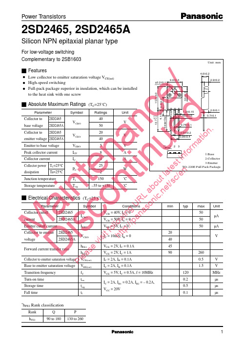
123Request for your special attention and precautions in using the technical information andsemiconductors described in this book(1)If any of the products or technical information described in this book is to be exported or provided to non-residents, the laws andregulations of the exporting country, especially, those with regard to security export control, must be observed. (2)The technical information described in this book is intended only to show the main characteristics and application circuit examplesof the products, and no license is granted under any intellectual property right or other right owned by our company or any other company. Therefore, no responsibility is assumed by our company as to the infringement upon any such right owned by any other company which may arise as a result of the use of technical information described in this book.(3)The products described in this book are intended to be used for standard applications or general electronic equipment (such as officeequipment, communications equipment, measuring instruments and household appliances). Consult our sales staff in advance for information on the following applications:– Special applications (such as for airplanes, aerospace, automobiles, traffic control equipment, combustion equipment, life support systems and safety devices) in which exceptional quality and reliability are required, or if the failure or malfunction of the prod-ucts may directly jeopardize life or harm the human body.– Any applications other than the standard applications intended.(4)The products and product specifications described in this book are subject to change without notice for modification and/or im-provement. At the final stage of your design, purchasing, or use of the products, therefore, ask for the most up-to-date Product Standards in advance to make sure that the latest specifications satisfy your requirements. (5)When designing your equipment, comply with the range of absolute maximum rating and the guaranteed operating conditions(operating power supply voltage and operating environment etc.). Especially, please be careful not to exceed the range of absolute maximum rating on the transient state, such as power-on, power-off and mode-switching. Otherwise, we will not be liable for any defect which may arise later in your equipment.Even when the products are used within the guaranteed values, take into the consideration of incidence of break down and failure mode, possible to occur to semiconductor products. Measures on the systems such as redundant design, arresting the spread of fire or preventing glitch are recommended in order to prevent physical injury, fire, social damages, for example, by using the products.(6)Comply with the instructions for use in order to prevent breakdown and characteristics change due to external factors (ESD, EOS,thermal stress and mechanical stress) at the time of handling, mounting or at customer's process. When using products for which damp-proof packing is required, satisfy the conditions, such as shelf life and the elapsed time since first opening the packages.(7)This book may be not reprinted or reproduced whether wholly or partially, without the prior written permission of MatsushitaElectric Industrial Co., Ltd.M a i n t e n a n D i s c o n t i n u eP le a s ev i s it f o l l o w i n g U R L a b o u t l a t e s t i n fo r mh t t p ://p a n a s o n i c .n e t /s c /e n。
2SD555中文资料
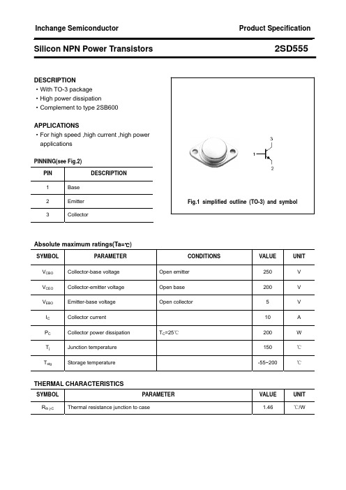
2SD555
MAX
UNIT V V
1.5 5.0 2.0 0.1 0.1 200
V V V mA mA
pF MHz
2
元器件交易网
Inchange Semiconductor Produicon NPN Power Transistors
元器件交易网
Inchange Semiconductor Product Specification
Silicon NPN Power Transistors
2SD555
DESCRIPTION ·With TO-3 package ·High power dissipation ·Complement to type 2SB600 APPLICATIONS ·For high speed ,high current ,high power applications
THERMAL CHARACTERISTICS
SYMBOL Rth j-C PARAMETER Thermal resistance junction to case VALUE 1.46 UNIT ℃/W
元器件交易网
Inchange Semiconductor Product Specification
PINNING(see Fig.2) PIN 1 2 3 Base Emitter Collector Fig.1 simplified outline (TO-3) and symbol DESCRIPTION
Absolute maximum ratings(Ta=℃)
SYMBOL VCBO VCEO VEBO IC PC Tj Tstg PARAMETER Collector-base voltage Collector-emitter voltage Emitter-base voltage Collector current Collector power dissipation Junction temperature Storage temperature TC=25℃ CONDITIONS Open emitter Open base Open collector VALUE 250 200 5 10 200 150 -55~200 UNIT V V V A W ℃ ℃
2SD1525中文资料
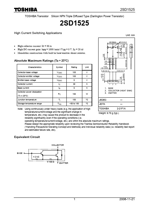
TOSHIBA Transistor Silicon NPN Triple Diffused Type (Darlington Power Transistor)2SD1525High Current Switching Applications• High collector current: I C = 30 A• High DC current gain: h FE = 1000 (min) (V CE = 5 V, I C = 20 A) • Monolithic construction with built-in base-emitter shunt resistor.Absolute Maximum Ratings (Ta = 25°C)Characteristics Symbol Rating UnitCollector-base voltage V CBO 100 V Collector-emitter voltage V CEO 100 V Emitter-base voltage V EBO 5 V Collector current I C30 A Base currentI B 5 A Collector power dissipation (Tc = 25°C)P C 150 WJunction temperature T j 150 °C Storage temperature rangeT stg−55 to 150°CNote: Using continuously under heavy loads (e.g. the application of high temperature/current/voltage and the significant change intemperature, etc.) may cause this product to decrease in the reliability significantly even if the operating conditions (i.e.operating temperature/current/voltage, etc.) are within the absolute maximum ratings.Please design the appropriate reliability upon reviewing the Toshiba Semiconductor Reliability Handbook(“Handling Precautions”/Derating Concept and Methods) and individual reliability data (i.e. reliability test report and estimated failure rate, etc).Equivalent CircuitUnit: mmJEDEC ― JEITA―TOSHIBA 2-21F1A Weight: 9.75 g (typ.)BASEElectrical Characteristics (Ta = 25°C)Markinglead (Pb)-free finish.Collector-emitter voltage V CE (V)I C – V CEC ol l ec t o r c u r r e n t I C (A )h FE – I CD C c u r r en t g a i n h F ECollector current I C (A)V CE (sat) – I CC o l l e c t o r -e m i t t e r s a t u r a t i onv o l t a g eV CE (s a t ) (V )Collector current I C (A)V BE (sat) – I CB a s e -e m i t t e r s a t u r a t i on v o l t age V B E (sa t ) (V )Collector current I C (A)Safe Operating AreaCo l l ec t o r c u r r e n t IC (A )Base-emitter voltage V BE (V)I C – V BEC o l l e c t o r c u r r e n t I C (A )Collector-emitter voltage V CE (V)5 30 100 300 210RESTRICTIONS ON PRODUCT USE20070701-EN •The information contained herein is subject to change without notice.•TOSHIBA is continually working to improve the quality and reliability of its products. Nevertheless, semiconductor devices in general can malfunction or fail due to their inherent electrical sensitivity and vulnerability to physical stress. It is the responsibility of the buyer, when utilizing TOSHIBA products, to comply with the standards of safety in making a safe design for the entire system, and to avoid situations in which a malfunction or failure of such TOSHIBA products could cause loss of human life, bodily injury or damage to property.In developing your designs, please ensure that TOSHIBA products are used within specified operating ranges as set forth in the most recent TOSHIBA products specifications. Also, please keep in mind the precautions and conditions set forth in the “Handling Guide for Semiconductor Devices,” or “TOSHIBA Semiconductor Reliability Handbook” etc.• The TOSHIBA products listed in this document are intended for usage in general electronics applications (computer, personal equipment, office equipment, measuring equipment, industrial robotics, domestic appliances, etc.).These TOSHIBA products are neither intended nor warranted for usage in equipment that requires extraordinarily high quality and/or reliability or a malfunction or failure of which may cause loss of human life or bodily injury (“Unintended Usage”). Unintended Usage include atomic energy control instruments, airplane or spaceship instruments, transportation instruments, traffic signal instruments, combustion control instruments, medical instruments, all types of safety devices, etc.. Unintended Usage of TOSHIBA products listed in his document shall be made at the customer’s own risk.•The products described in this document shall not be used or embedded to any downstream products of which manufacture, use and/or sale are prohibited under any applicable laws and regulations.• The information contained herein is presented only as a guide for the applications of our products. No responsibility is assumed by TOSHIBA for any infringements of patents or other rights of the third parties which may result from its use. No license is granted by implication or otherwise under any patents or other rights of TOSHIBA or the third parties.• Please contact your sales representative for product-by-product details in this document regarding RoHS compatibility. Please use these products in this document in compliance with all applicable laws and regulations that regulate the inclusion or use of controlled substances. Toshiba assumes no liability for damage or losses occurring as a result of noncompliance with applicable laws and regulations.。
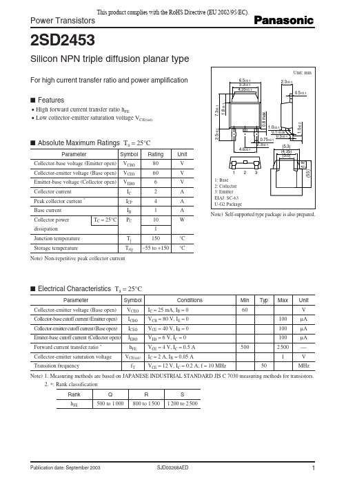
2SD2453R中文资料
0.6
0.5mA 0.4mA
6
0.4
0.3mA 0.2mA
2
4
2
0.2
0.1mA
1
0
0
0 40 80 120 160 200
0
2
4
6
8
10
12
0 0 0.2 0.4 0.6 0.8 1.0 1.2
Ambient temperature Ta (°C)
Collector-emitter voltage VCE (V)
1.0
IB=1.2mA 1mA 5 TC=25˚C
IC VBE
Collector power dissipation PC (W)
10
0.8
4 0.7mA 0.6mA
25˚C
Collector current IC (A)
8
Collector current IC (A)
TC=100˚C 3
–25˚C
Note) 1. Measuring methods are based on JAPANESE INDUSTRIAL STANDARD JIS C 7030 measuring methods for transistors. 2. *: Rank classification Rank hFE Q 500 to 1 000 R 800 to 1 500 S 1 200 to 2 500
0.01
1
10
100
1 000
Collector-emitter voltage VCE (V)
2
SJD00268AED
Request for your special attention and precautions in using the technical information and semiconductors described in this book
2SD2425资料
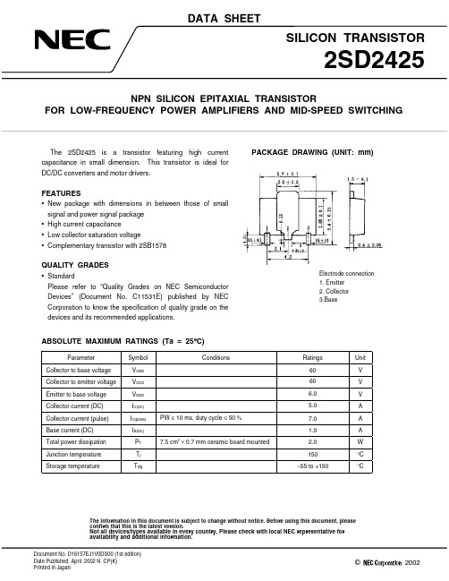
1998©Document No. D16157EJ1V0DS00 (1st edition)Date Published April 2002 N CP(K)Printed in JapanSILICON TRANSISTOR2SD2425NPN SILICON EPITAXIAL TRANSISTORFOR LOW-FREQUENCY POWER AMPLIFIERS AND MID-SPEED SWITCHINGDATA SHEET2002The information in this document is subject to change without notice. Before using this document, please confirm that this is the latest version.Not all devices/types available in every country. Please check with local NEC representative for availability and additional information.The 2SD2425 is a transistor featuring high current capacitance in small dimension. This transistor is ideal for DC/DC converters and motor drivers.FEATURES•New package with dimensions in between those of small signal and power signal package •High current capacitance •Low collector saturation voltage •Complementary transistor with 2SB1578QUALITY GRADES•StandardP lease refer to “Quality Grades on NEC Semiconductor Devices” (Document No. C11531E) published by NEC Corporation to know the specification of quality grade on the devices and its recommended applications.PACKAGE DRAWING (UNIT: mm)ABSOLUTE MAXIMUM RATINGS (Ta = 25°C)ParameterSymbol ConditionsRatings Unit Collector to base voltage V CBO 60V Collector to emitter voltage V CEO 60V Emitter to base voltage V EBO 6.0V Collector current (DC)I C(DC) 5.0A Collector current (pulse)I C(pulse)PW ≤ 10 ms, duty cycle ≤ 50 %7.0A Base current (DC)I B(DC) 1.0A Total power dissipation P T 7.5 cm 2 × 0.7 mm ceramic board mounted 2.0W Junction temperature T j 150°C Storage temperatureT stg−55 to +150°CElectrode connection 1. Emitter 2. Collector 3.BaseData Sheet D16157EJ1V0DS2ELECTRICAL CHARACTERISTICS (Ta = 25°C)ParameterSymbol ConditionsMIN.TYP.MAX.UnitCollector cutoff current I CBO V CB = 50 V, I E = 010µA Emitter cutoff currentI EBO V EB = 6.0 V, I C = 010µA DC current gain h FE1V CE = 1.0 V, I C = 0.1 A 60180−DC current gain h FE2V CE = 1.0 V, I C = 2.0 A 100200400−DC current gainh FE3V CE = 2.0 V, I C = 5.0 A 50150−Collector saturation voltage V CE(sat)I C = 2.0 A, I B = 0.2 A 90300mV Base saturation voltage V BE(sat)I C = 2.0 A, I B = 0.2 A 0.9 1.2VTurn-on time t on 0.6µs Storage time t stg 0.8µs Fall timet fI C = 2.0 A, V CC = 10 V I B1 = −I B2 = 0.2 A R L = 5.0 Ω0.08µsh FE CLASSIFICATIONMarking AB1AB2AB3h FE2100 to 200160 to 320200 to 400TYPICAL CHARACTERISTICS (Ta = 25°C)Data Sheet D16157EJ1V0DS34Data Sheet D16157EJ1V0DS[MEMO]Data Sheet D16157EJ1V0DS5M8E 00. 4The information in this document is current as of July, 2001. The information is subject to change without notice. For actual design-in, refer to the latest publications of NEC's data sheets or data books, etc., for the most up-to-date specifications of NEC semiconductor products. Not all products and/or types are available in every country. Please check with an NEC sales representative for availability and additional information.No part of this document may be copied or reproduced in any form or by any means without prior written consent of NEC. NEC assumes no responsibility for any errors that may appear in this document.NEC does not assume any liability for infringement of patents, copyrights or other intellectual property rights of third parties by or arising from the use of NEC semiconductor products listed in this document or any other liability arising from the use of such products. No license, express, implied or otherwise, is granted under any patents, copyrights or other intellectual property rights of NEC or others.Descriptions of circuits, software and other related information in this document are provided for illustrative purposes in semiconductor product operation and application examples. The incorporation of these circuits, software and information in the design of customer's equipment shall be done under the full responsibility of customer. NEC assumes no responsibility for any losses incurred by customers or third parties arising from the use of these circuits, software and information.While NEC endeavours to enhance the quality, reliability and safety of NEC semiconductor products, customers agree and acknowledge that the possibility of defects thereof cannot be eliminated entirely. To minimize risks of damage to property or injury (including death) to persons arising from defects in NEC semiconductor products, customers must incorporate sufficient safety measures in their design, such as redundancy, fire-containment, and anti-failure features.NEC semiconductor products are classified into the following three quality grades:"Standard", "Special" and "Specific". The "Specific" quality grade applies only to semiconductor products developed based on a customer-designated "quality assurance program" for a specific application. The recommended applications of a semiconductor product depend on its quality grade, as indicated below. Customers must check the quality grade of each semiconductor product before using it in a particular application."Standard":Computers, office equipment, communications equipment, test and measurement equipment, audioand visual equipment, home electronic appliances, machine tools, personal electronic equipment and industrial robots"Special":Transportation equipment (automobiles, trains, ships, etc.), traffic control systems, anti-disastersystems, anti-crime systems, safety equipment and medical equipment (not specifically designed for life support)"Specific":Aircraft, aerospace equipment, submersible repeaters, nuclear reactor control systems, lifesupport systems and medical equipment for life support, etc.The quality grade of NEC semiconductor products is "Standard" unless otherwise expressly specified in NEC's data sheets or data books, etc. If customers wish to use NEC semiconductor products in applications not intended by NEC, they must contact an NEC sales representative in advance to determine NEC's willingness to support a given application.(Note)(1)"NEC" as used in this statement means NEC Corporation and also includes its majority-owned subsidiaries.(2)"NEC semiconductor products" means any semiconductor product developed or manufactured by or forNEC (as defined above).••••••。
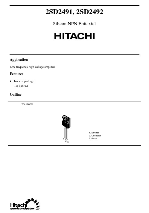
2SD2492中文资料
2SD2491, 2SD2492Silicon NPN EpitaxialApplicationLow frequency high voltage amplifierFeatures• Isolated packageTO-126FMOutline2SD2491, 2SD24922Absolute Maximum Ratings (Ta = 25°C)RatingsItemSymbol 2SD24912SD2492Unit Collector to base voltage V CBO 160200V Collector to emitter voltage V CEO 160200V Emitter to base voltage V EBO 55V Collector currentI C 100100mA Collector power dissipation P C 1.35 1.35W Collector power dissipation P C *188W Junction temperature Tj 150150°C Storage temperature Tstg–55 to +150–55 to +150°CNote:1.Value at T C = 25°CElectrical Characteristics (Ta = 25°C)2SD24912SD2492ItemSymbol Min Typ Max Min Typ Max Unit Test conditions Collector to base breakdown voltage V (BR)CBO 160——200——V I C = 10 µA, I E = 0Collector to emitter breakdown voltage V (BR)CEO 160——200——V I C = 1 mA, R BE = ∞Emitter to base breakdown voltage V (BR)EBO 5——5——V I E = 10 µA, I C = 0Collector cutoff currentI CBO——10———µA V CB = 140 V, I E = 0—————10µAV CB = 160 V, I E = 0DC current transfer ratio h FE1*160—32060—320V CE = 5 V, I C = 10 mA DC current transfer ratio h FE230——30——V CE = 5 V, I C = 1 mA Base to emitter voltage V BE —— 1.5—— 1.5V V CE = 5 V, I C = 10 mA Collector to emitter saturation voltage V CE(sat)——2——2V I C = 30 mA, I B = 3 mA Gain bandwidth product f T—140——140—MHz V CE = 5 V, I C = 10 mA Collector output capacitance Cob—3.8——3.8—pF V CB = 10 V, I E = 0f = 1 MHzNote: 1.The 2SD2491 and 2SD2492 are grouped by h FE1 and its specification is as follows.B CD60 to 120100 to 200160 to 3202SD2491, 2SD2492 See characteristic curves of 2SD1609, 2SD1610.3Unit: mm 元器件交易网Cautions1.Hitachi neither warrants nor grants licenses of any rights of Hitachi’s or any third party’s patent,copyright, trademark, or other intellectual property rights for information contained in this document.Hitachi bears no responsibility for problems that may arise with third party’s rights, includingintellectual property rights, in connection with use of the information contained in this document.2.Products and product specifications may be subject to change without notice. Confirm that you have received the latest product standards or specifications before final design, purchase or use.3.Hitachi makes every attempt to ensure that its products are of high quality and reliability. However,contact Hitachi’s sales office before using the product in an application that demands especially high quality and reliability or where its failure or malfunction may directly threaten human life or cause risk of bodily injury, such as aerospace, aeronautics, nuclear power, combustion control, transportation,traffic, safety equipment or medical equipment for life support.4.Design your application so that the product is used within the ranges guaranteed by Hitachi particularly for maximum rating, operating supply voltage range, heat radiation characteristics, installationconditions and other characteristics. Hitachi bears no responsibility for failure or damage when used beyond the guaranteed ranges. Even within the guaranteed ranges, consider normally foreseeable failure rates or failure modes in semiconductor devices and employ systemic measures such as fail-safes, so that the equipment incorporating Hitachi product does not cause bodily injury, fire or other consequential damage due to operation of the Hitachi product.5.This product is not designed to be radiation resistant.6.No one is permitted to reproduce or duplicate, in any form, the whole or part of this document without written approval from Hitachi.7.Contact Hitachi’s sales office for any questions regarding this document or Hitachi semiconductor products.Hitachi, Ltd.Semiconductor & Integrated Circuits.Nippon Bldg., 2-6-2, Ohte-machi, Chiyoda-ku, Tokyo 100-0004, Japan Tel: Tokyo (03) 3270-2111 Fax: (03) 3270-5109Copyright ' Hitachi, Ltd., 1999. All rights reserved. Printed in Japan.Hitachi Asia Pte. Ltd.16 Collyer Quay #20-00Hitachi TowerSingapore 049318Tel: 535-2100Fax: 535-1533URLNorthAmerica : http:/Europe : /hel/ecg Asia (Singapore): .sg/grp3/sicd/index.htm Asia (Taiwan): /E/Product/SICD_Frame.htm Asia (HongKong): /eng/bo/grp3/index.htm Japan : http://www.hitachi.co.jp/Sicd/indx.htmHitachi Asia Ltd.Taipei Branch Office3F, Hung Kuo Building. No.167, Tun-Hwa North Road, Taipei (105)Tel: <886> (2) 2718-3666Fax: <886> (2) 2718-8180Hitachi Asia (Hong Kong) Ltd.Group III (Electronic Components)7/F., North Tower, World Finance Centre,Harbour City, Canton Road, Tsim Sha Tsui,Kowloon, Hong Kong Tel: <852> (2) 735 9218Fax: <852> (2) 730 0281 Telex: 40815 HITEC HXHitachi Europe Ltd.Electronic Components Group.Whitebrook ParkLower Cookham Road MaidenheadBerkshire SL6 8YA, United Kingdom Tel: <44> (1628) 585000Fax: <44> (1628) 778322Hitachi Europe GmbHElectronic components Group Dornacher Stra§e 3D-85622 Feldkirchen, Munich GermanyTel: <49> (89) 9 9180-0Fax: <49> (89) 9 29 30 00Hitachi Semiconductor (America) Inc.179 East Tasman Drive,San Jose,CA 95134 Tel: <1> (408) 433-1990Fax: <1>(408) 433-0223For further information write to:。
2SD2150中文资料
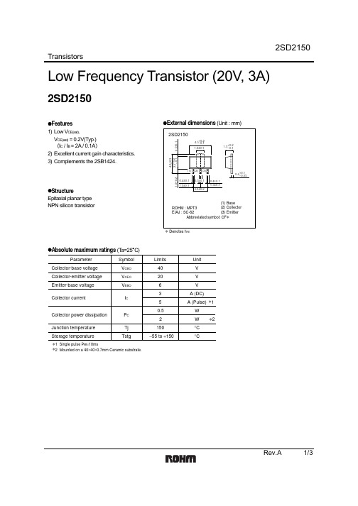
TransistorsRev.A 1/3Low Frequency Transistor (20V, 3A)2SD2150z Features 1) Low V CE(sat).V CE(sat) = 0.2V(Typ.) (I C / I B = 2A / 0.1A )2) Excellent current gain characteristics. 3) Complements the 2SB1424.z StructureEpitaxial planar type NPN silicon transistorz External dimensions (Unit : mm)Denotes h FEz Absolute maximum ratings (T a=25°C)ParameterV CBO V CEO V EBO I CP C Tj Tstg40V V V A (DC)W W°C °C2063 A (Pulse)50.52∗1∗2150−55 to +150Symbol Limits Unit ∗1 Single pulse Pw =10ms∗2 Mounted on a 40×40×0.7mm Ceramic substrate.Collector-base voltage Collector-emitter voltage Emitter-base voltage Collector currentCollector power dissipation Junction temperature Storage temperatureTransistorsRev.A 2/3z Electrical characteristics (T a=25°C)ParameterSymbol BV CBO BV CEO BV EBO I CBO I EBO h FE V CE(sat)f T CobMin.40206−−120−−−−−−−−−0.229025−−−0.10.15600.5−−V I C =50µA I C =1mA I E =50µA V CB =30V V EB =5VV CE =2V, I C =0.1AI C /I B =2A/0.1A V CE =2V, I E = −0.5A, f =100MHz V CE =10V, I E =0A, f =1MHzV VµA µA −V ∗MHz pFTyp.Max.Unit Conditions∗ Measured using pulse current.Collector-base breakdown voltage Collector-emitter breakdown voltage Emitter-base breakdown voltage Collector cutoff current Emitter cutoff currentDC current transfer ratio Collector-emitter saturation voltageTransition frequency Output capacitancez Packaging specifications and h FEPackage CodeT1001000Taping Basic ordering unit (pieces)RSh FE 2SD2150Typeh FE values are classified as follows :Item h FER 180 to 390S 270 to 560z Electrical characteristic curvesC O L L E C T O R C U R R E N T : I C (A )BASE TO EMITTER VOLTAGE : V BE (V)Fig.1 Grounded emitter propagationcharacteristicsC O L L E C T O R C U R R E N T : I C(A )COLLECTOR TO EMITTER VOLTAGE : V CE (V)Fig.2 Grounded emitter outputcharacteristics ( ) C O L L E C T O R C U R R E N T : I C (A )COLLECTOR TO EMITTER VOLTAGE : V CE (V)Fig.3 Grounded emitter outputcharacteristics ( )TransistorsRev.A 3/3D C C U R RE N T G A I N : hF ECOLLECTOR CURRENT : I C (A)Fig.4 DC current gain vs.collector currentC O L L E C T O R S A T U R A T I O N V O L T A G E : V C E (s a t ) (V )COLLECTOR CURRENT : I C (A)Fig.6 Collector-emittersaturation voltage vs.collector curren ( )C O L L E C T O R S A T U R A T I O N V O L T A G E : V C E (s a t ) (V )COLLECTOR CURRENT : I C (A)Fig.5 Collector-emittersaturation voltage vs. collector current ( )C O L L E C T O R O U T P U T C A P A C I T A N C E : C o b (p F )E M I T T E R I N P U T C A P A C I T A N C E : C i b (p F )COLLECTOR TO BASE VOLTAGE : V CB (V)EMITTER TO BASE VOLTAGE : V EB (V)Fig.9 Collector output capacitance vs.collector-base voltageEmitter input capacitance vs.emitter-base voltageC O L L E C T O R S A T U R A T I O N V O L T A G E : V C E (s a t ) (V )COLLECTOR CURRENT : I C (A)Fig.7 Collector-emittersaturation voltage vs.collector current ( )T R A N S I T I O N F R E Q U E N C Y : f T (M H z )EMITTER CURRENT : I E (mA)Fig.8 Gain bandwidth product vs.emitter currentAppendixAbout Export Control Order in JapanProducts described herein are the objects of controlled goods in Annex 1 (Item 16) of Export T rade ControlOrder in Japan.In case of export from Japan, please confirm if it applies to "objective" criteria or an "informed" (by MITI clause)on the basis of "catch all controls for Non-Proliferation of Weapons of Mass Destruction.Appendix1-Rev1.1。
2SD2498中文资料

2SD2498中⽂资料TOSHIBA TRANSISTOR SILICON NPN TRIPLE DIFFUSED MESA TYPE2SD2498HORIZONTAL DEFLECTION OUTPUT FOR HIGH RESOLUTION DISPLAY, COLOR TVHIGH SPEED SWITCHING APPLICATIONSz High Voltage: V CBO = 1500 V z Low Saturation Voltage : V CE (sat) = 5 V (Max.) z High Speed : t f = 0.4 µs (Typ.)z Collector Metal (Fin) is Fully Covered with Mold ResinABSOLUTE MAXIMUM RATINGS (Tc = 25°C)CHARACTERISTIC SYMBOL RATING UNITCollector ?Base Voltage V CBO 1500 V Collector ?Emitter Voltage V CEO 600 V Emitter ?Base Voltage V EBO5 V DC I C6 Collector Current Pulse I CP12ABase CurrentI B 3 A Collector Power Dissipation P C 50 W Junction Temperature T j 150 °C Storage Temperature RangeT stg55~150 °CNote: Using continuously under heavy loads (e.g. the application of hightemperature/current/voltage and the significant change in temperature, etc.) may cause this product to decrease in the reliability significantly even if the operating conditions (i.e. operating temperature/current/voltage, etc.) are within the absolute maximum ratings.Please design the appropriate reliability upon reviewing the Toshiba Semiconductor Reliability Handbook(“Handling Precautions”/Derating Concept and Methods) and individual reliability data (i.e. reliability test report and estimated failure rate, etc).MARKINGUnit: mmJEDEC ― JEITA―TOSHIBA 2-16E3A Weight: 5.5 g (typ.)lead (Pb)-free package or lead (Pb)-free finish.D2498ELECTRICAL CHARACTERISTICS (Tc = 25°C)CHARACTERISTIC SYMBOL TEST CONDITION MINTYP. MAX UNIT Collector Cut ?off Current I CBO V CB = 1500 V, I E = 0 ―― 1 mA Emitter Cut ?off Current I EBO V EB = 5 V, I C = 0 ―― 10 µA Collector ?Emitter BreakdownVoltageV (BR) CEO I C = 10 mA, I B = 0 600―― Vh FE (1) V CE = 5 V, I C = 1 A 10 ― 30 DC Current Gainh FE (2) V CE = 5 V, I C = 4A 5 ― 9―Collector ?Emitter Saturation VoltageV CE (sat) I C = 4A, I B = 0.8 A ―― 5 VBase ?Emitter Saturation VoltageV BE (sat) I C = 4 A, I B = 0.8 A ― 0.9 1.2 V Transition Frequency f T V CE = 10 V, I C = 0.1 A ― 2 ― MHz Collector Output Capacitance C ob V CB = 10 V, I E = 0, f = 1 MHz ― 95 ― pF Storage Time t stg ― 7 10Switching Time (Fig.1)Fall Timet fI CP = 4 A, I B1 (end) = 0.8 A f H = 15.75 kHz― 0.4 0.7µsFig.1 SWITCHING TIME TEST CIRCUITRESTRICTIONS ON PRODUCT USE20070701-EN ?The information contained herein is subject to change without notice.TOSHIBA is continually working to improve the quality and reliability of its products. Nevertheless, semiconductor devices in general can malfunction or fail due to their inherent electrical sensitivity and vulnerability to physical stress. It is the responsibility of the buyer, when utilizing TOSHIBA products, to comply with the standards of safety in making a safe design for the entire system, and to avoid situations in which a malfunction or failure of such TOSHIBA products could cause loss of human life, bodily injury or damage to property.In developing your designs, please ensure that TOSHIBA products are used within specified operating ranges as set forth in the most recent TOSHIBA products specifications. Also, please keep in mind the precautions and conditions set forth in the “Handling Guide for Semiconductor Devices,” or “TOSHIBA Semiconductor Reliability Handbook” etc.The TOSHIBA products listed in this document are intended for usage in general electronics applications (computer, personal equipment, office equipment, measuring equipment, industrial robotics, domestic appliances, etc.).These TOSHIBA products are neither intended nor warranted for usage in equipment that requires extraordinarily high quality and/or reliability or a malfunction or failure of which may cause loss of human life or bodily injury (“Unintended Usage”). Unintended Usage include atomic energy control instruments, airplane or spaceship instruments, transportation instruments, traffic signal instruments, combustion control instruments, medical instruments, all types of safety devices, etc.. Unintended Usage of TOSHIBA products listed in his document shall be made at the customer’s own risk.The products described in this document shall not be used or embedded to any downstream products of which manufacture, use and/or sale are prohibited under any applicable laws and regulations. The information contained herein is presented only as a guide for the applications of our products. No responsibility is assumed by TOSHIBA for any infringements of patents or other rights of the third parties which may result from its use. No license is granted by implication or otherwise under any patents or other rights of TOSHIBA or the third parties.Please contact your sales representative for product-by-product details in this document regarding RoHS compatibility. Please use these products in this document in compliance with all applicable laws and regulations that regulate the inclusion or use of controlled substances. Toshiba assumes no liability for damage or losses occurring as a result of noncompliance with applicable laws and regulations.。
