集成光学课程第八章-1
光学教程第四版 姚启钧著 讲义第八章.8

25
四、选 模
在激光器的输出光束 中,如果只存在一个共振 频率,则称为一个纵向模 式或称为纵向单模,简称 单纵模。在激光技术中, 如同时存在几个共振频率, 则称为纵向多模。
可利用F-P标准具进
行选模,条件是:
k
k
c 2nd cos i2
.
26
8.6 激光的相干性
一、时间相干性和空间相干性 二、普通光源的相干性 三、激光器的横向模式 四、激光的相干性
27
一、时间相干性和空间相干性
相干性:空间任意两点光振动之间相互关联的 程度。
相干时间:原子的平均发光时间间隔△tH 。
相干长度:在相干时间内光经过的路程△lH ,
△lH = c △tH 。
迈克耳孙干涉仪————光的时间相干性;
杨氏实验——光源的空间相干性。
二、普通光源的相干性
n B n u(v) n
21
21 2
2 21
其中B21 称为受激辐射爱因斯坦系数。
17
注意:
①
只有当外来光子的能量
h
正好
21
满足关系式
h 21 E2 E1
时,才能引起受激辐射。
② 受激辐射发出来的光子与外来光 子具有相同的频率、相同的发射方向、 相同的偏振态和相同的相位。
3
8. 7 激光器的种类 8. 8 非线性光学 8. 9 全息照相 8.10 光盘存储技术 8.11 傅立叶光学的几个基本概念 8.12 阿贝成像原理 8.13 阿贝-波特实验和空间滤波
4
8.1 原子发光的机理
一、玻尔的氢原子模型 二、能级图 三、原子发光的机理
第八章 晶体的光学效应 OF 季家镕 高等光学教程
第八章 晶体的光学效应在第七章所介绍的晶体光学基本知识的基础上,本章中介绍晶体由于外加场的作用而产生的各种光学效应,其中包括电光效应、弹光效应、声光效应、磁光效应等。
目前,根据这些效应制成的器件在光电技术中已经得到了广泛的应用。
§8.1 晶体的电光效应一、电光效应概述1、逆相对介电张量η的定义和它的主值在§7.3节中我们定义了相对介电张量εr 的逆张量ηε=−r 1 (8.1-1)称之为逆相对介电张量。
在§7.1中已经证明了,在无损耗不旋光的介质中介电张量εr 是一个对称张量,由上式可以证明在此条件下必定也是一个对称张量,其张量元ηηηij ji = (8.1-2)由各向异性介质中的物质方程D =ε0εr E 和(8.1-1)式得到E =10εηD (8.1-3)晶体中电场能量密度由 (7.1-17) 式给出,即ωe =⋅12E D (8.1-4) 将(8.1-3)式代入上式,得02e εω⋅=ηD D (8.1-5)上式就是 e ij j iji D D ωεη02=∑ (,,,)i j X Y Z = (8.1-6)或e X Z ZX Z Y YZ Y X XY Z ZZ Y YY X XX D D D D D D D D D ωεηηηηηη02222222=+++++(8.1-7)上式表明,在空间中光波场的等能面是一个椭球面,作变量代换 D X e D X ωε021=, Y e D Y ωε021= , Z e D Z ωε021= (8.1-8)(8.1-7)式化为 ηηηηηηXX YY ZZ XY YZ ZX X Y Z XY YZ ZX 222222+++++0= (8.1-9) 采用坐标旋转的方法,使新坐标系中的x 、、轴与椭球的三个对称轴重合,于是在新坐标系中(8.1-9)式化为y z364ηηη1122223321x y z ++= (8.1-10)式中,η11、η22、η33就是逆相对介电张量的主值,与主轴坐标系中波法线椭球方程x n y n z n x y z 2221++= (8.1-11)相比较,可见在没有外加电场时逆相对介电张量的主值η1121=n x , η2221=n y , η3321=n z(8.1-12) 在主轴坐标系中张量元ηη12210== , ηη13310== , ηη23320== (8.1-13)2、线性电光效应和二次电光效应简介根据固体的量子理论,介质的逆相对介电张量取决于电荷在晶体中的分布,当一个外加电场作用于晶体时,会导致内部束缚电荷的重新分布,且可能导致离子晶格的微小形变。
第21次课(第八章)工程光学

远摄物镜
工程光学 (上)
★焦距变化的变倍比为 ★焦距为
第六节 摄影系统
第五级北航仪器 光电学院
MA fmax 23 k max
f min
23 k min
f'
f
' 1
2
3
k
变焦物镜
工程光学
第八节 变焦距光学系统
(上) 一、变焦距光学系统的原理
第五级北航仪器 光电学院
(一)变焦距的物理意义 ★焦距连续变化,物、像面保持不动。
❖ 目镜只是把物镜的像放大,放大倍率再高也不能把物镜不能分辨的物 体细节看清。
有效放大率:为充分利用物镜的分辨率,使被物镜分辨出的细节同 时能被眼睛看清,满足这一条件的放大率。
前面我们介绍人眼的角分辨为:60〞。为了使人眼观察比较舒服, 一般取2'~4',照明波长为0.555μm,可得:
工程光学 (上)
双高斯物镜
工程光学 (上)
★广角摄影物镜
第六节 摄影系统
焦距:f 70.4mm 相对孔径:D / f 1: 6.8 视场角: 122o
第五级北航仪器 光电学院
广角物镜
工程光学 (上)
★远摄摄影物镜
第六节 摄影系统
焦距:f 3m 相对孔径:D / f 1: 6
视场角:2<30o
第五级北航仪器 光电学院
500NA 1000NA
工程光学
第四节 望远镜系统
(上)
一、一般特性
第五级北航仪器 光电学院
望远镜的组成:由物镜和目镜组成。
物镜的像方焦点与目镜的物方焦点重合,光学间隙Δ=0。
开普勒望远镜
工程光学 (上)
第四节 望远镜系统
《集成光学课程简介》课件

认真阅读教材和课件,掌握基 本概念和原理
实验与实践环节安排
光波导器件实验
了解光波导器件的基本原理和特性
光子集成电路实验
了解光子集成电路的设计和制作过程
光子晶体实验
探究光子晶体的禁带特性和光子局域特性
应用领域实践
结合实际应用,进行集成光学器件的设计和 制作
THANK YOU
感谢聆听
总结词
集成光学通信系统利用集成光学器件 实现高速、大容量的光通信。
详细描述
集成光学通信系统具有传输速率高、 传输距离远、保密性好等优点,可应 用于数据中心、云计算等领域。
04
集成光学的前沿技术与发展趋势
光子晶体技术
总结词
光子晶体是一种具有光子带隙的人工微结构材料,能够控制光子在特定频率范围 内的传播。
光波导器件的基本原理
80%
光波导器件定义
利用光波导原理制成的各种光学 器件,如分束器、耦合器、调制 器等。
100%
光波导器件的工作原理
通过改变光波导的结构、形状或 材料参数等手段,实现对光波导 中光的操控,从而实现不同的光 学功能。
80%
光波导器件的应用
在光纤通信、光计算、光传感等 领域有广泛的应用。
详细描述
光子晶体技术利用光子晶体对光的独特调控能力,在集成光学领域中实现了一系 列创新应用,如光子晶体激光器、光子晶体光纤等。光子晶体技术为集成光学的 发展提供了新的可能性,有望在未来实现更高效、更紧凑的光子器件。
光子集成电路技术
总结词
光子集成电路是一种集成了多个光器件的光波导型集成回路,可以实现光信号的产生、调制、探测等功能。
详细描述
集成光子器件具有高效、紧凑、低成本等优点,可实现光信 号的产生、调制、探测等功能,广泛应用于光通信、光计算 等领域。
《集成光学课程简介》课件
发展历程
集成光学的历史可以追溯到20世纪60年代,当时还只是一个小众领域的研究 方向。经过几十年的发展,现在集成光学已经广泛应用于光纤通信、传感、 医疗等领域,成为了光学技术的重要分支。
基本原理
波导结构
集成光学器件的基本组成部分 是波导结构,它通过控制介质 折射率的变化,将光束导引在 芯片中进行传输。
总结和展望
通过学习本课程,我们了解到了集成光学领域的基础知识、应用以及未来发展方向。在未来,集成光学 有望在电子信息以及医疗等诸多领域发挥重要作用,成为推动技术进步和社会发展的重要力量。
《集成光学课程简介》 PPT课件
本课程旨在介绍集成光学的基本原理、器件分类、应用以及未来展望。欢迎 大家一同探索这个迅猛发展的领域。
概述
随着信息技术的发展,集成光学已经走到了人们的视野里。集成光学通过将光学器件集成在同一芯片上, 使得光的传输更加高效、稳定。今天,我们就来一窥这一重要技术的发展历程及基本原理。
干涉效应
利用干涉效应可以实现光的调 制和解调,是集成光学器件实 现信号处理的基本原理。
光子晶体
光子晶体是新型的光学材料, 它的光子带隙结构可以实现对 于不同波长光的筛选和传输, 因而成为了制备光滤波器的重 要方法。
器件分类介绍
光开关
光开关是一种能够在线路中实现光学信号转 换的集成器件,从而实现光的调控、切换等 功能。
光开关网络
2
长的光信号合并在一起进行传输,提 高通讯网络的传输能力。
通过光开关器件的调控,可以实现拓
扑结构的改变,从而更好地满足不同
网络应用的需求。
3
光纤传输
光集成技术实现了大规模的光分路器 以及复杂的光学网络,为光纤通信的 发展提供了重要的支撑。
《集成光学理论与技术》习题答案C1

C1 导论1.1 阐述与金属导体相比,光纤互连的四个优势。
1) 抗电磁干扰能力强。
2) 在军事及高度机密的应用中,光纤能比有线电或者无线电通信线路提供更好的防窃听或监视能力。
3) 损耗低,可长程传输光信号。
4) 可同时传输多路信号,通信容量远高于金属导体。
(可密集捆束通过金属管道而不必考虑电绝缘问题;易燃易爆环境,光纤断裂不会产生电火花。
)1.2 阐述与集成电路技术相比,集成光路技术的四个优势。
1)工作带宽大;2)抗电磁干扰能力强;3)不存在短路问题;4)制备材料丰富,便宜;5)在易燃易爆环境下更为安全。
……1.3 混合集成与单片集成光路的区别是什么?每种类型各有什么优缺点?主要区别是混合集成使用两种或两种以上的衬底制备集成光路的不同组件,再把这些组件组装在一起;而单片集成光路在同一块衬底材料上制备所有的组件构成完整的集成光路。
前者的优点是可以以最佳的材料最佳的工艺分别制备各组件达到最佳性能,缺点是后续工序复杂,组装困难。
后者的优点是一次成型,如果批量生产,成本可以大大降低。
主要缺点是很难做到所有器件具有最佳性能,需要折中。
主要原因是不同的器件需要不同工艺、不同材料。
1.4 为什么在集成光路的制作中,采用GaAs、GaAlAs和GaInAsP几种特别有用的材料?Why are GaAs, GaAlAs and GaInAsP particularly useful materials for the fabrication of optical integrated circuits?1)有源材料,辐射波长在0.65~1.7µm之间;2)在0.6~12µm之间具有很好的透光性;3)晶格失配小;4) 电光系数、声光品质因子大,可以用于开关、调制器件;5)外延、参杂、刻蚀等技术成熟;6) 成本低于其他III-V(或者II-VI)族材料。
集成光学系统设计课程教学大纲

陈益新等编译,集成光学理论与技术,上海交通大学出版社,1999
1. 课程性质、目的和任务
本课程是信息工程各专业本科生必修的一门工程专业课。通过本课程的学习,使学生掌握集成光学设计的基本理论和方法,获得解决有关实际问题的能力。
大纲审定者:潘武
大纲批准者:张德民
大纲校对者:王艳
集成光学(Integrated Optics) 课程考试大纲
一、课程编号:020332
二、课程类型:工程科学
课程学时:64学时(其中理论教学16学时/1学分,实践教学48学时/3学分)
适用专业:光信息科学与技术专业
先修课程:光传输技术基础,光学原理,信息光学
三、概述
1. 考试目的:检验学生对集成光学基本理论及设计的掌握程度
2. 考试基本要求:根据集成光学课程大纲的要求进行考核。
3. 考试形式:堂上闭卷
四、考试内容及范围
考试内容为授课计划(基于教学大纲)中讲授的要求理解和掌握的内容,考试范围为教学大纲要求的范围。
五、考试对象
光信息科学与技术专业光信息方向所有学生以及其他方向选修本课程的学生。
集成光学课程教学大纲
课程英文名称:Integrated Optics
课程编号:020332
课程类型:工程科学
学时:64学时(其中理论教学16学时/1学分,实践教学48学时/3学分)
适应对象:光信息科学与技术专业
先修课程:光传输技术基础,光学原理,信息光学
使用教材:西原 浩,春名正光,栖原敏明 著,梁瑞林 译, 集成光路,科学出版社,2004
集成光学概论教案课件

• 《Introduction to optical waveguide analysis: Solving Maxwell’s equations and the Schrödinger Equation》, KENJI KAWANO and TSUTOMU KITOH, Wiley, 2001
• 按集成的类型划分:光子集成回路(PIC)和光电 子集成回路(OEIC)
• 按集成的技术途径划分:单片集成和混合集成 • 按研究内容划分:导波光学和集成光路
3.集成光学的定义
(1)集成光学是在光电子学和微电子学基础上, 采用集成方法研究和发展光学器件和混合光学 -电子学器件系统的一门新的学科。
(2)集成光学是研究介质薄膜中的光学现象, 以及光学元器件集成化的一门学科。
参考书目
• 《集成光学器件导论》,陈福深、杨拥军、孙豹 等,机械工业 出版社,2010年1月第1版
• 《光波导原理与器件》,宋贵才、全薇、蔡红星、雷建国 等, 清华大学出版社,2012年1月第1版
• 《高等光学仿真(MATLAB版):光波导·激光》,欧攀,北京 航空航天大学出版社,2011年7月第1版
集成光学概论 1.1 集成光学的概念 1.2 集成光学的特点 1.3 集成光学的发展和现状 1.4 研究集成光学的意义
§1.1 集成光学的概念
1. 集成电路(integrated circuit, IC)
1947年,贝尔研究所的肖克利(Shockley)、巴丁 (Bardeen)、布拉顿(Brattain)发明晶体管 1957年,得克萨斯仪器公司的基尔毕(Kirby)发明集成电路 2006年,被集成的晶体管个数达到两亿个;2010年,美 国英特尔集成了23亿个晶体管(当时的最高水平)。 “集成”成为了一种潜力难以估量的科学技术手段。
成都工业学院电子科学与技术集成光学复习资料

第一章概论1.1集成光学的概念集成光学的理论基础是光学和光电子学,涉及波动光学与信息光学、非线性光学、半导体光电子学、晶体光学、薄膜光学、导波光学、耦合模与参量作用理论、薄膜光波导器件和体系等多方面的现代光学内容;其工艺基础则主要是薄膜技术和微电子工艺技术。
1.2集成光学的特点离散光学元件系统的缺点:体积和重量大、稳定性差和光束的调准困难。
集成光学系统的优点:①光波在光波导中传播,光波容易控制和保持其能量②集成化带来的稳固定位。
对振动和温度等环境因素的适应性比较强,最大优点。
③器件尺寸和相互作用长度缩短;相关的电子器件的工作电压也较低。
④功率密度高。
⑤体积小、重量轻。
集成光路代替集成电路的优点:1.带宽增加;2.光子器件中光子运动速度比电子器件中运动速度高得多,且没有导线电容和电感对频率的限制;3.实现“波分多路复用”;4.实现多路开关;5.尺寸小,重量轻,功耗小6.成批制备经济性好,可靠性高。
7.降低成本(制造、应用、维护、升级)1.4 研究集成光学的意义(开放题)1.信息光电子技术改变着人类的生存和发展方式,在未来的信息社会中必将扮演重要的角色,成为21世纪的基石和支柱之一。
2.信息光电子技术也是保障国防安全的核心技术之一。
3.光电子技术在信息领域的应用中迅速发展且有独特的优势。
4.集成光学集中并发展了光学和微电子学的固有技术优势,将传统的由分立器件构成的庞大的光学系统变革为集成光学系统。
5.集成光学系统作为现代光电子学的一个重要分支,研究集成光学十分重要。
第二章平面介质光波导和耦合模理论用于集成光学中的光波导根据结构分为平板波导和条形波导。
平面波导(仅在x方向具有折射率差)条形光波导(在x、y方向上限制光场)平板波导由三层介质构成:波导层:中间层,介质折射率n1最大覆盖层:上包层,折射率n3<n1衬底层:下包层,折射率n2<n1。
n2=n3,称为对称型平板波导。
反之,称为非对称型波导。
在集成光学中使用的最多的是埋入型波导。
集成光学-01
-用集成光路代替集成电路 -用导光波的介质平面光波导和光 学纤维代替电线或者同轴电缆
集成光学的特点
• 集成光学系统与离散光学器件系 统的比较 • 集成光路与集成电路的系统的比较
• 离散光学器件系统
-非集成,组装和调整困难 -器件体积和重量大,构成的系统大约 是l平方米的数量级,光束的粗细大约为 1cm -稳定性差,光束的调准困难
集成光路与集成电路的比较
光纤与电传输线的比较
光纤与双绞线电缆损耗的比较
光纤与电传输线的比较
光纤与同轴电缆损耗的比较
光纤与电传输线的比较
• 光纤的优点
-带宽很宽,传输的信息量大 -传输损耗小 -电磁干扰小 -不存在电的短路或接地问题 -在易燃区安全 -保密性好,难于窃听 -尺寸小,重量轻 -价格低廉,原材料丰富
集成光学的发展和现状
• 发展
1962年开发出半导体同质结激光二极管 1963年提出双异质结构半导体激光二极管, 并对其工作原理作了深入研究 1967年出现的异质结外延生长技术,拉开 了半导体激光器实用化的序幕 1970年实现激光二极管的室温连续工作 1970年研制成功低损耗光纤
集成光学的发展和现状
• 国际 ※ 研究及交流活跃,起步较早 -1972年,美国光学协会主办集成光学 主题会议 • 国内 ※ 1970年开始研究,发展迅速
集成光学的发展和现状
• 当前研究热点
在很大程度上提高集成光学器件的可靠性和 稳定性 减小波导传输损耗、降低散射 减小器件尺寸,提高集成度 期待光路/光元件的集成化 提高光通信用多波长光源的性能、成本、可 靠性 突破目前的“光-电-光”交换的瓶颈 进一步改善开关/调制器的消光比
集 成
光
学
集成光学考试总结---精品管理资料

第一章1. 集成光学的分类:•按集成的方式划分:个数集成和功能集成•按集成的类型划分:光子集成回路(PIC)和光电子集成回路(OEIC)•按集成的技术途径划分:单片集成和混合集成•按研究内容划分:导波光学和集成光路2. 集成光学的定义(1)集成光学是在光电子学和微电子学基础上,采用集成方法研究和发展光学器件和混合光学-电子学器件系统的一门新的学科。
(2)集成光学是研究介质薄膜中的光学现象,以及光学元器件集成化的一门学科。
(3)集成光学是研究集成光路的特性和制造技术以及与微电子学相结合的学科。
3. 集成光学的主要应用光纤通信,光子计算机,光纤传感4. 集成光学系统有什么优点?1)集成光学系统与离散光学器件系统的比较(1)光波在光波导中传播,光波容易控制和保持其能量。
(2)集成化带来的稳固定位。
(3)器件尺寸和相互作用长度缩短;相关的电子器件的工作电压也较低.(4)功率密度高.沿波导传输的光被限制在狭小的局部空间,导致较高的功率密度,容易达到必要的器件工作阈值和利用非线性效应工作。
(5)体积小,重量轻。
集成光学器件一般集成在厘米尺度的衬底上,其体积小,重量轻。
2)集成光路与集成电路的比较把激光器、调制器、探测器等有源器件集成在同一衬底上,并用光波导、隔离器、耦合器和滤波器等无源器件连接起来构成的光学系统称为集成光路,以实现光学系统的薄膜化、微型化和集成化。
用集成光路代替集成电路的优点包括带宽增加,波分复用,多路开关.耦合损耗小,尺寸小,重量轻,功耗小,成批制备经济性好,可靠性高等。
由于光和物质的多种相互作用,还可以在集成光路的构成中,利用诸如光电效应、电光效应、声光效应、磁光效应、热光效应等多种物理效应,实现新型的器件功能。
第二章1. 光波导的分类(a)平板波导(slab waveguide)(b)条形波导(strip waveguide)(c)圆柱波导(cylindrical waveguide)2。
集成光学 第八章-2
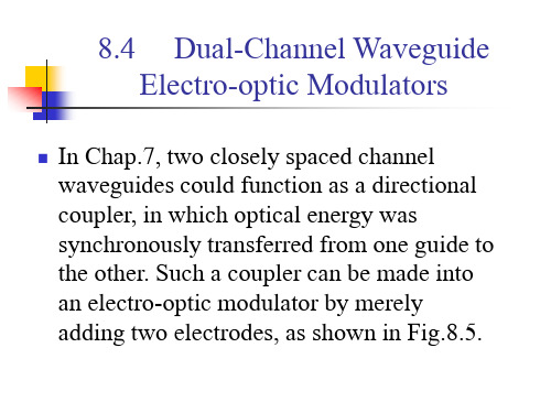
8.4 Dual-Channel WaveguideElectro-optic ModulatorsIn Chap.7, two closely spaced channel waveguides could function as a directional coupler, in which optical energy was synchronously transferred from one guide to the other. Such a coupler can be made into an electro-optic modulator by merely adding two electrodes, as shown in Fig.8.5.Fig.8.5 Basic dual-channel modulator structure8.4.1 Theory of OperationIf a modulating signal voltage is applied to the electrodes, as shown in Fig.8.5, it produces a slight difference in the indices of refraction in the guides, which results in a propagation constant difference . By once again following the coupled mode theory approach used in Chap.7, the coupling equations can be shown to be given by)()()(1000z A i z A i dz z dA κβ--=(8.4.1))()()(0111z A i z A i dzz dA κβ--=(8.4.2)where β0and β1are the propagation constants in the two guides, and the other terms have already been defined previously. The solution of (8.4.1) and (8.4.2), subject to the boundary conditions that A 0(0)=1 and A 1(0)=0(8.4.3)yields the following expressions for A 0(z ) and A 1(z ).⎥⎦⎤⎢⎣⎡⎪⎭⎫ ⎝⎛∆--⎪⎪⎭⎫ ⎝⎛∆-=z i gz g i gz z A 2exp sin 2cos )(00βββ⎥⎦⎤⎢⎣⎡⎪⎭⎫ ⎝⎛∆+-⎪⎪⎭⎫ ⎝⎛--=z i gz g i z A 2exp sin )(11ββκ(8.4.4)(8.4.5)where 10βββ-=∆2222⎪⎭⎫ ⎝⎛∆+=βκg (8.4.6)Thus, in this case of imperfect phase match, the power flow in the two guides is given by z z e g gz egz z A z A z P ααβ--⎪⎭⎫ ⎝⎛∆+==2222*000)(sin 2)(cos )()()((8.4.7)z e gz g z A z A z P ακ-==)(sin )()()(222*111(8.4.8)where αis the exponential loss coefficient in the guides. Note that (8.4.7) and (8.4.8) become identical to (7.2.12) and (7.2.13) when ∆βequals zero.2222⎪⎭⎫ ⎝⎛∆+=βκgThus, the condition for total transfer of power for zero applied voltage is given once again by (7.2.14), which states thatκπκπm L +=2(8.4.9)where m=0,1,2,…. Similarly, it can be seen from (8.4.7) and (8.4.8) that, when a modulating voltage is applied to produce a ∆β, the coupling is completely cancelled [i.e., P 1(L )=0 and P 0(L )=1] ifππm gL +=m=0,1,2,...(8.4.10)From (8.4.9) and (8.4.10) it can be shown that the value of required for 100% modulation is given by πβ3)(=∆L (8.4.11)The effective index of refraction in a guide is given by k n g β=(8.4.12)Thus, the change in effective index needed for 100% modulation is given bykL n g π3=∆(8.4.13)In typical cases, the magnitude of ∆n g required for 100% modulation is surprisingly small. For example, in a GaAlAs 3μm x3μm dual-channel waveguide modulator such as that of Fig.8.5, of length equal to 1cm, (8.4.13) predicts that light of 900nm vacuum wavelength can be totally switched by producing a ∆n g of approximately 1x10⁻⁴. From (8.3.3) it can be determined that the magnitude of the required electric field is about 3x10⁴V/cm, corresponding to a voltage of 10V across the 3μm thick channels.⏹The particular modulator geometry shown in Fig.8.5 is probably the simplest arrangement that can be envisioned, so that it serves as a good example to illustrate the principles of dual-channel modulator operation.⏹A problem is that the length of the device must be carefully chosen to establish maximum coupling with no applied bias, as per (8.4.9); the on state cannot be electrically adjusted.Fig.8.6 Topographic view of dual-channel modulator with split electrodes to produce a stepped reversal.Kogelnik and Schmidt have demonstrated a dual-channel modulator in which three basic electrodes are split in half, as shown in Fig.8.6.The polarity of the applied voltage is reversed in the two halves to produce two sections with ∆βof equal magnitude, but opposite sign. The effect of this stepped ∆βreversal is to yield a device in which both the off and on states can be electrically adjusted for a relative wide range of lengths. Obviously this allows one to maximize the extinction ration and minimize crosstalk.They showed that providing sections with alternating makes it possible to cause a complete transfer of the light from one waveguide to another by electrical adjustment of the on and off states, as long as the ratio L/l is greater than unity, where L is the total length of the modulator, and l is the effective interaction length.8.5 Mach-Zehnder Type Electro-Optic ModulatorsAnother class of modulators is based on a waveguide version of the Mach-Zehnder interferometer, in which interference is produced between phase coherent light waves that have traveled over different path lengths. The basic modulator structure is shown in Fig.8.7. Light input to the modulator is via a single-mode waveguide. A beam splitter divides the light into two equal beams that travel through guides a and b, respectively. By applying a voltage to the electrodes, the effective path lengths can be varied.Fig.8.7 Mach-Zehner type modulatorIn an ideally designed modulator of this type, the path lengths and guide characteristics are identical, so that with no applied voltage the split beams recombine in the output waveguide to produce the lowest-order mode once more. If an electric field is applied so as to produce a phase change of radians between the two arms, then the recombination results in an optical field that is zero at the center of the output waveguide, corresponding to the first order (m=1) mode. If the output waveguide is a single mode guide, identical to the input guide, the first order mode is cut off, and rapidly dissipates over a short length by substrated radiation. Thus, the modulator can be switched from a transmitting to a non-transmitting state of by application of a voltage.Various embodiments of the basic Mach-Zehner interferometer structure of Fig.8.7 have been demonstrated to be effective. One problem with all of the Mach-Zehner modulators described thus far is that even minute variations in fabrication parameters result in a device which is not in the on state for zero applied voltage. Thus, careful control of the applied voltage must be maintained for both the off and on states.Ramaswamy et al. have gone one step further by using electrically switched dual-channel directional couplers as the beam splitter and combiner. This modification permits electrical adjustment of both the splitting fractions and the phase change in the interferometer arms. Thus, the off and on states can be electrically selected for optimum extinction ratio.8.6 Electro-Optic Modulators Employing Reflection or Diffraction A number of different modulators and switches have been demonstrated that utilize electro-optic control of either reflection or diffraction of the waveguided light. Diffraction modulators are generally based on the Bragg effect, which involves distributed interactions with multiple reflecting elements, usually in the form of an optical grating.8.6.1 Bragg-Effect Electro-Optic ModulatorsA typical Bragg-effect modulators is show in Fig.8.8, which consists of an interlaced, comb like, pair of electrodes. A voltage applied to the interdigitated surface electrodes perturbs the index of refraction beneath them, thus forming an effective optical grating pattern in the waveguide. This grating causes a change in the direction of propagation of the light beam. If the direction of the light beam in the waveguide is adjusted so it is incident onto the grating bars at an angle equalto the Bragg angle θB, the light is diffracted with maximum efficiency at an angle 2θB with respect to the input beam.Fig.8.8 Bragg-effect electro-optic modulatorIt can be shown that θB is given by)2(sin 0g B n Λ=λθ(8.6.1)where Λis the grating spacing, and n g is the effective guide index (β/k).The derivation of (8.6.1) is based on the thick grating assumption that 202Λ>>L πλ(8.6.2)If the input beam strikes the grating at an angle different from the Bragg angle, diffraction still occurs over a limited range of ∆θB , but with reduced efficiency.The angular range for a 50% reduction is given byLB Λ=∆2θ(8.6.3)For small θB such that sin θB ≈θB .The intensity of light diffracted is dependent on the applied voltage, and has the general form)(sin 20VB I I =(8.6.4)where I is the intensity of the diffracted beam with V applied, I 0is the transmitted intensity with V=0, and B is a constant dependent on the effective guide index and on the applicable element of the electro-optic tensor.8.6.2 Electro-optic Reflection Modulators It is possible to use the linear electro-optic effect to reduce the index of refraction in a layer, thereby bringing about the total internal reflection of an optical beam. A device of this type is shown in Fig.8.9. Four horn-shaped tapered channel waveguides form the input and output ports to a planar waveguide modulator which contains a region in which the refractive index can be reduced by application of an electric field.Fig.8.9 A total internal reflection (TIR) electro-optic modulator and switchIf there is no applied voltage, an incident light beam from, for example, port 1 will encounter no index interface and will pass freely to port 4. If the horn tapers are carefully designed and fabricated to minimize scattering and mode conversion, very little crosstalk will occur at port 3. However, when a voltage is applied with the proper polarity to reduce the index between the electrodes, two interfaces are created between regions of different index. Total internal reflection may occur at the first interface if the angle of incidence is greater than the critical angle, thereby causing partial (or possible total) switching of the light beam to port 3.A TIR (total internal reflection) switch of the type described has been fabricated by Tsai et al. by Ti diffusion of Y cut LiNbO3. Theinput/output horns were 4.7 mm long, tapering from 4 to 40 μm in width. The length of the electrode pair was L=3.4 mm and d equaled4μm. Complete switching of a 632.8 nm beam was observed for V approximately equal to 50V. Cross-talk to port 3 in the absence of an applied voltage was measured to be 15 dB.8.7 Comparison of Waveguide Modulatorsto Bulk Electro-Optic ModulatorsAt several places in this chapter, the relatively low drive power required by a waveguide modulator has been noted. To quantitatively compare the power requirements of a waveguide modulator to those of a bulk electro-optic modulator, it is convenient to develop a simple, yet general, expression for the average external power P e needed to operate the modulator at a maximum frequency equal to its bandwidth ( f).For the case of 100% modulation, this power is given by n e E f P )(∆=(8.7.1)where E n is the energy supplied from an external source to switch the device on or off. For an ideal electro-optic modulator with no Ohmic losses, all of this energy goes into the stored electric field between the electrodes. Hence, we can take2)(2dV E E a V n ⎰=ε(8.7.2)where E a is the peak amplitude of the applied field, and εis the permittivity. The integral is to be taken over the entire volume occupied by the field.If we assume, for convenient, that all of the electric field is confined to the modulator volume, and additionally that E a is uniform over that volume, (8.7.2) becomes2)(2a n WtLE E ε=(8.7.3)where W is the width, t is the thickness and L is the length for the modulator active volume. Hence, the external drive power, from (8.7.1), is given by2)(2a e WtLE f P ε∆=(8.7.4)The key feature of (8.7.4) is that the modulating power required is proportional to the active volume. Thus, if we compare a bulk electro-optic modulator, such as that shown in Fig.8.10a, to the planar waveguide modulator of Fig.8.10b, it is obvious that significantly less power is required by the planar waveguide devices. Still greater power reduction is obtained by going to a channel waveguide modulator, such as that shown in Fig.8.10c. Consider the following numerical example.For the specific case of an electro-optic modulator formed in GaAs with the orientation shown in Fig.8.1, we find by using(8.3.3) that the applied field and the resulting change in index of refraction are related byFig.8.10 Basic electro-opticmodulator structures; (a) bulk;(b) planar waveguide; (c)channel waveguide)()2(4132r n n E a ∆=(8.7.5)Therefore, combining (8.7.5) and (8.7.4) yields 224162)(2n r n WtL f P e ∆∆=ε(8.7.6)For the special case of the dual-channel 100% modulator, it has been shown in (8.4.13) that )2()3()()3(0L kL n λπ==∆(8.7.7)Substituting (8.7.7) into (8.7.6) gives the expressionL r n Wt f P e 241622023)(λε=∆(8.7.8)If we take the following typical values for GaAs: W =6x10⁻⁶m, t =3x10⁻⁶m, λ0=0.9x10⁻⁶m, n 2=3.6, r 41=1.2x10⁻¹²m/V , ε/ε0=12, and L =0.5cm, the result is that P e /(∆f )=0.148mW/MHz. The comparable value of for a planar waveguide modulator would typically be on the order of ten times larger because of the increase in W, while that for a bulk modulator would be 100 to 1000 times larger because of corresponding increases in both W and t .It should be noted that the values of P e /(∆f ) calculated using (8.7.6) are based on the assumption that the optical fields and the electric field are both uniformly confined to a volume WtL . If this is not the case, a slightly modified relation can be used, which is given by 22416221))(()(2n r n L c t c W f P e ∆∆=ε(8.7.9)where c 1and c 2are constants, having a value less than 1, to account for electric field and optical field not being perfectly confined to the same volume.In this chapter, a number of different types of electro-optic modulators have been discussed.Problems8.1 We wish to design a GaP electro-optic phase modulator as shown in the figure for operation at 630nm wavelength. a) What is the minimumthickness (t) required in the waveguiding layer if the carrier concentrations are N2=1x1015cm-3andN3=3x1018cm-3? b) How large a voltage (V) can be applied without producing electrical breakdown? c) Ifthis voltage is applied, how long (L) must the device be to produce a phase shift of radians in the transmitted light wave? Assume the incident light ispolarized in the Y direction.E c(critical electric field for breakdown): 5x10⁵V/cm, r41(electro-optic coefficient for the above orientation):5x10-11cm/V, m* (effective mass): 0.013m0, n2=3.2.8.2 In the electro-optic waveguide switch shown in the figure, how large a voltage (V) must be applied to the electrode to turn the waveguide on ---i.e., to increase the index of refraction in the waveguide sufficiently so as to bring it above cutoff for the lowest order waveguide mode?Assume: 1) Wavelength of light in air λ0=1.0μm. 2) Effective mass of electron m*=0.08m e. 3) All of the voltage is dropped over the waveguide thickness rather than in the substrate. 4) Crystal orientation is such that r41is the appropriate electro-optic tensor element to be used, and positive voltage (V) produces an increase in index of refraction.。
《信息光学》第八章 光学信息处理(修订版)

其中,
fx x2 f
fy y2 f
b f sin
上式中的三、四项包含了所需的滤波函数H和H*,只要参考光倾角足够大,在滤 波运算时,各项的作用互不干扰。
若滤波函数H是复函数,则
x x x y y y H 2 , 2 H 2 , 2 exp j 2 , 2 f f f f f f
相干滤波包括两个过程:从输入面到频谱面的频率分解过程和从频谱面到
输出面的频率合成过程。若在频谱面放置一特定的滤波器,则实现了对输入 信息的变换处理! 4f系统是非常典型的相干滤波系统。
利用透镜的傅立叶变换性质,可实现相干光处理或相干滤波。前面介绍的
2.4 其 他的相 干滤波 系统
2、相干滤波的基本原理 根据滤波器的特点,可以将滤波器分成以下几种:
T fx H fx T f x
aL sin c Lf x d
P3面输出光场分布为
g x3 F -1 T f x H f x
t x3
a x rect 3 d L
2、相干滤波的基本原理
2.3 相干滤波的基本原理和运算
1 f A x3 2b, y3 exp j f B x3 2b, y3 exp j 4
如果=0,在P3平面中心部位就实现了图像的相加; 如何实现图像相减呢? 其他四项分别位于(b,0)和(2b,0)的位置。
4、光栅滤波器的应用——图像加减和微分
Fs f x , f y XYcomb Xf x comb Yf y F f x , f y
3、简单振幅和位相滤波的例子
3.2 位相滤波 位相滤波是指改变各种频率成份的相对位相分布,其中1935年荷兰物 理学家泽尼克发明的相衬法就是位相滤波的杰出范例。 相衬法的基本原理:
集成光学概论教学课件

1.2.2 集成光路与集成电路的比较
把激光器、调制器、探测器等有源器件集成在同一衬底上, 并用光波导、隔离器、耦合器和滤波器等无源器件连接起来 构成的微型光学系统称为集成光路,以实现光学系统的薄膜 化、微型化和集成化。 用集成光路代替集成电路的优点包括带宽增加,波分复用, 多路开关。耦合损耗小,尺寸小,重量轻,功耗小,成批 制备经济性好,可靠性高等。由于光和物质的多种相互作 用,还可以在集成光路的构成中,利用诸如光电效应、电 光效应、声光效应、磁光效应、热光效应等多种物理效应, 实现新型的器件功能。
光子计算机:
光子计算机是一种全新的计算机,是以光子作为主要的信息 载体,以光子系统作为计算机的主体,以光运算作为计算机 运算方式的计算机。
光子计算机的优点:
(a)具有超高的运算速度 ——串行电子计算机的极限速度是1010次/秒, 而 光 子 计 算 机 的 理 论 计 算 速 度 达 1023 次 / 秒 , 在 技 术 上 可 实 现 1012~1015次/秒的计算速度
参考书目
• 《集成光学器件导论》,陈福深、杨拥军、孙豹 等,机械工业 出版社,2010年1月第1版
• 《光波导原理与器件》,宋贵才、全薇、蔡红星、雷建国 等, 清华大学出版社,2012年1月第1版
• 《高等光学仿真(MATLAB版):光波导·激光》,欧攀,北京 航空航天大学出版社,2011年7月第1版
1970年研制成功了低损耗光纤,目前光纤的传输损耗已经降 低到了0.2dB/km以下。 1972年,Somekh和Yariv提出了在同一个半导体衬底上同 时集成光器件和电子器件的构想。
1987 年 , Yablonovitch 和 John 大 约 同 时 提 出 了 光 子 晶 体 (photonic crystal, PC)的概念。
华中科技大学 《应用光学》课程PPT——第八章 光线的光路计算

d 2 , , Lk Lk 1 d k 1 L2 L1 d1 , L3 L2 , , U k U k 1 U 2 U 1 , U 3 U 2 , n3 n 2 , , n k n k 1 n2 n1
光线计算类型
A
B
得子午象差和弧矢象差,全面了解 系统的成象特性。
§ 8-2 子午面内的光线光路计算公式
例如,求组合光学系统的各个参数
1. 轴上点近轴光线的光路计算(第一近轴光线)
, u3 u 2 , u k u k 1 u 2 u1 d 2 , , lk lk 1 d k 1 l2 l1 d1 , l3 l2 n n , n n , , n n 1 3 2 k k 1 2
求系统焦距
f '
h1 10 / 0.100104 99.8961 u3 '
注:当用近轴光计算公式第二式和过渡公式计算发生错误,校对公 式是发现不了的。
2. 轴外点近轴光线的光路计算及象高(第二近轴光线)
y 已知l,y,lZ,则: u z lz l
相当于已知lZ和uZ,求lZ ′和uZ ′ 理想象高:
P1
A -y
y' l ' z l 'u z
-u1 -uz P2 lz-l
P
O1
目的:利用轴上点的近轴公式来 计算轴外点近轴光光线
B
-lz
用近轴光线光路计算公式和 校对公式,所有量均注以下标z
二、轴上点远轴光线的光路计算
1. 计算公式: 2. 转面公式:
Lr sin I r sin U n sin I ' in I n' U ' U I I ' L' r r sin I ' sin U '
集成光学教学设计

集成光学教学设计背景介绍集成光学是一种新型的光学技术,具有高速传输、大带宽、低插入损耗等优点,在通信、计算机网络、数据处理等领域得到了广泛应用。
因此,集成光学教学也越来越重要。
本文将重点探讨如何进行集成光学教学设计,以帮助教师更好地开展课程教学。
设计目标集成光学教学设计的主要目标是培养学生的集成光学专业知识和实践技能,同时让学生了解集成光学的应用场景和未来发展趋势。
具体而言,集成光学教学设计应该满足以下要求:知识目标•理解集成光学的基本原理和特点;•掌握集成光学芯片的光学布局和制作工艺;•熟悉集成光学器件的性能参数和测试方法。
技能目标•掌握集成光学器件的设计和模拟方法;•熟练掌握集成光学器件的制作和测试技术;•能够利用集成光学技术设计和搭建光学通信系统。
价值目标•增强学生的实际操作能力和创新思维;•提高学生的团队合作和沟通能力;•培养学生的集成光学应用意识和实践能力。
设计内容集成光学教学设计的内容应该紧密围绕知识目标、技能目标和价值目标展开,同时考虑到课程的实际情况和学生的个体差异。
以下是一些可能的设计内容:理论教学•集成光学的基本概念和相关知识点;•集成光学器件的设计原理和布局要点;•集成光学器件的制作工艺和测试方法。
实验教学•集成光学器件的制作和测试实验;•集成光学光学器件的性能参数测试实验;•集成光学器件在光通信系统中的应用实验。
综合设计•集成光学器件的设计和模拟;•集成光学器件的制作和测试;•集成光学器件在光通信系统中的应用设计。
设计方法设计一门集成光学教学课程需要科学的教学方法。
以下是一些可能的教学方法:课堂讲授课堂讲授是集成光学教学的基础,教师可以通过讲解理论知识、案例分析、实验演示等形式,让学生了解集成光学的基本原理和应用领域,培养学生的批判性思维和创新能力。
实验实践实验实践是集成光学教学的重要组成部分,通过实验让学生亲身体验集成光学的制作和测试过程,加深学生对集成光学器件的理解和认识。
- 1、下载文档前请自行甄别文档内容的完整性,平台不提供额外的编辑、内容补充、找答案等附加服务。
- 2、"仅部分预览"的文档,不可在线预览部分如存在完整性等问题,可反馈申请退款(可完整预览的文档不适用该条件!)。
- 3、如文档侵犯您的权益,请联系客服反馈,我们会尽快为您处理(人工客服工作时间:9:00-18:30)。
Electro-Optic Modulators⏹8.1 Basic Operating Characteristics of Switches andModulators⏹8.2 The Electro-Optic Effect⏹8.3 Single-Waveguide Electro-Optic Modulators⏹8.4 Dual-Channel Waveguide Electro-optic Modulators ⏹8.5 Mach-Zehnder Type Electro-Optic Modulators⏹8.6 Electro-Optic Modulators Employing Reflection orDiffraction⏹8.7 Comparison of Waveguide Modulators to BulkElectro-Optic Modulators在本章将学到⏹单波导电光调制器的工作原理⏹双沟道波导电光调制器的工作原理⏹波导调制器比“体”调制器更为优越⏹如何设计波导电光调制器重点掌握单波导电光调制器和双沟道波导电光调制器的工作原理⏹modulator:调制器⏹switch:开关⏹modulation depth:调制深度⏹bandwidth:带宽⏹insertion loss:插入损耗⏹power consumption:功率损耗⏹isolation:隔离度⏹Pockels effect:普克尔效应⏹Kerr effect:克尔效应⏹indicatrix:指标线;光率体⏹index ellipsoid:折射率椭球⏹centrosymmetric:中心对称的⏹single-waveguide electro-optic modulators:单波导电光调制器⏹phase modulator:相位调制器⏹polarizer:起偏器⏹polarization–selective filter(usually called an analyzer):检偏器⏹intensity modulator:强度调制器⏹electro-absorption modulator:电致吸收调制器⏹Franz-Keldysh effect:弗兰茨-凯第希效应(当一半导体材料中存在强电场时,材料的吸收光谱向长波方向移动)⏹direct bandgap material:直接带隙材料⏹depletion layer:耗尽层⏹Mach-Zehnder interferometer:马赫---泽德干涉仪⏹Permittivity:介电常数This chapter begins the discussion of optical-signal modulation and switching. In many cases, the same device can function as either a modulator or a switch, depending on the strength of the interaction between the optical waves and the controlling electrical signal, as well as on the arrangement of input and output ports. The device is considered to be a modulator if its primary function is to impress information on a light wave by temporarily varying one of its properties. A switch, on the other hand, changes the spatial position of the light, or else turns it off and on.8.1 Basic Operating Characteristicsof Switches and ModulatorsOne important characteristic of modulators and switches is the modulation depth, or modulation index, η. In the case of an intensity modulator in which the applied electrical signal acts to decrease of thetransmitted light, ηis given by00)(I I I -=η(8.1.1)where I is the transmitted intensity and I 0is the value of I with no electrical signal applied.8.1.1 Modulation Depthm I I I )(0-=η(8.1.2)where I m is the transmitted intensity when maximum signal is applied. The maximum modulation depth, or extinction ratio, is given by00m ax )(I I I m -=ηforI I m ≤(8.1.3)or by m o m I I I )(m ax -=ηfor 0I I m ≥(8.1.4)It is also possible to define the modulation depth for phase modulators, as long as the phase change can be functionally related to an equivalent intensity change.If the applied electrical signal acts to increase the transmitted light intensity, ηis given byFor the case of interference modulators, it can be shown that the modulation depth is given by)2(sin 2ϕη∆=(8.1.5)where ∆ϕis the phase change.Modulation depth has been defined for intensitymodulators (and indirectly for phase modulators); however, an analogous figure of merit, the maximum deviation of a frequency modulator, is given by00m ax f f f D m -=(8.1.6)where f 0is the optical carrier frequency, and f m is the shifted optical frequency when the maximum electrical signal is applied.8.1.2 BandwidthAnother important characteristic of modulators and switches is the bandwidth, or range of modulation frequencies over which the device can be operated. By convention, that bandwidth of a modulator is usually taken as the difference between the upper and lower frequencies at which the modulation depth falls to 50% of its maximum value. In the case of a switch, frequency response is usually given in terms of the switching speed, or switching time. The switching time T is related to the bandwidth ∆f by the expression=π2(8.1.7)fT∆Minimizing switching time is most important when large-scale arrays of switches are used to route optical waves over desired paths. Similarly, modulation bandwidth is a critical factor when information channels are to be multiplexed onto the same optical beam. Thus, the unusually fast switching speed and wide bandwidth of waveguide switches and modulators, which will be discussed later in this chapter, make them particularly useful in large telecommunications system.8.1.3 Insertion LossInsertion loss is another important characteristic of optical switches and modulators that must be known for system design. Insertion loss is generally stated in decibels, and for the case in which the modulating signal acts to decrease in the intensity, it is given by)log(100I I L t i (8.1.8)where I t is the optical intensity that would betransmitted by the waveguide if the modulator were absent, and I 0is the intensity transmitted with the modulator in place, but with no applied signal.For a modulator in which the applied signal acts to increase the transmitted intensity, the insertion loss is given by)log(10m t i I I L (8.1.9)where I m is the transmitted intensity whenmaximum signal is applied. Insertion loss is, of course, an optical power loss. However, it ultimately increases the amount of electrical power that must be supplied to the system, since higher power optical sources must be used.8.1.4 Power ConsumptionElectrical power must also be supplied to drive the modulator or switch. In the case of modulators, the required drive power increase with modulation frequency. Hence, a useful figure of merit is the drive power per unit bandwidth, P/∆f, usually expressed in milliwatts per megahertz. As is discussed in more detail in Sect.8.7, a key advantage of channel-waveguide modulators is that they have a significantly lower P/∆f than that required for bulk modulators.8.1.5 IsolationThe degree of isolation between variousinputs and outputs of a switch or modulator is a major design consideration. In a modulator, the isolation between input and output is merely the maximum modulation index, as defined previously. However, it is usually expressed in decibels when used to specify isolation. In the case of a switch, the isolation between two ports (either input or output) is given by21[]10log()isolation dB I I =-(8.1.10)where I1is the optical intensity in the driving port, and I2is the intensity at the driven port when the switch is in the off state with respect to port 1 and 2. Thus, a switch with a signal leakage, or crosstalk, of 1% with respect to two ports would have 20dB isolation.8.2 The Electro-Optic EffectThe fundamental phenomenon that accounts for the operation of most electro-optic modulators and switches is the change in index of refraction produced by the application of an electric field. In the most general case, this effect is non-isotropic, and contains both linear (Pockels effect)and nonlinear (Kerr effect)components. In crystalline solids, the change in index produced by the linear electro-optic effect, can be most conveniently characterized by the change in the components of the optical indicatrix matrix.The equation of the index ellipsoid in the presence of an electric field is1121212111625242232222212=⎪⎭⎫ ⎝⎛+⎪⎭⎫ ⎝⎛+⎪⎭⎫ ⎝⎛+⎪⎭⎫ ⎝⎛+⎪⎭⎫ ⎝⎛+⎪⎭⎫ ⎝⎛xy n xz n yz n z n y n x n (8.2.1)If x ,y , and z are chosen to be parallel to the principal dielectric axes of the crystal, the linear change in the coefficients due to an electric field E is given by∑==⎪⎭⎫ ⎝⎛∆3121j j ij i E r n (8.2.2)where i =1,2,3,4,5,6, and where j =1,2,3 are associated with x ,y ,z , respectively.If (8.2.2) is written in matrix form, the 6x3[r ij] matrix is called the electro-optic tensor. It can be shown that the linear electro-optic effect exists only in crystals that do not possess inversion symmetry. Even in the case of these non-centrosymmetric crystals, for most symmetry classes, only a few elements of the electro-optic tensor are nonzero. Hence, in the design of an electro-optic modulator or switch, both the waveguide material and its orientation with respect to the applied electric field must be chosen carefully. Nevertheless, many materials that can be used to make low loss waveguides, such as GaAs, GaP, LiNbO3, LiTaO3and quartz, also have significantly large Pockels coefficients, for certain orientation. Thus, the linear eletro-optic effect is widely used in integrated optic applications.The nonlinear (quadratic) Kerr electro-optic coefficient is relatively weak in commonly used waveguide materials. Also, a nonlinear dependence in electric field introduces unwanted modulation crossproducts (distortion) into the modulated signal. Consequently, it is not particularly useful in most integrated optic applications.8.3 Single-Waveguide Electro-OpticModulatorsThere are several different types of electro-optic modulators and switches that can be fabricated in a single-waveguide structure. The waveguide may be either a planar, or a channel guide. For example, the relatively simple planar waveguide shown in Fig.8.1 can function as either a phase modulator, an amplitude (intensity) modulator, or as an optical switch.Fig.8.1 Basic electro-optic modulator structureThe waveguide shown in Fig.8.1 is formed in Ga(1-x)Al x As using the hetero-epitaxial growth technique described in Chap 4. However, any electro-optic semiconductor such as GaAs x P(1-x), GaAs, or GaP could be used, and also the waveguide could alternatively be formed by the carrier-concentration-reduced method.8.3.1 Phase ModulationThe waveguide of Fig.8.1 is asymmetric, since the indices of the air and the metal at the top surface are both much less than n 2, while n 3is relatively close to n 2. The total change in index between the guide and the substrate is given by EO CCR chemical n n n n n ∆+∆+∆=-=∆3223(8.3.1)where ∆n chemical is the index change due to the differing aluminium concentrations a and b , ∆n CCR is the change resulting from decreased carrierconcentration (if any) in the guide, and ∆n EO is the index change caused by the electro-optic effect.To make a phase modulator, the dimensions and doping of the waveguide are chosen so that it is above cutoff for the m=0 mode at the wavelength desired, but is below cutoff for the m=1 mode. Thus, from (3.1.12)202202329321⎪⎪⎭⎫ ⎝⎛<∆+∆<⎪⎪⎭⎫ ⎝⎛g CCR chemical g t n n n t n λλ(8.3.2)When a voltage V is applied with reverse bias polarity to the Schottky barrier diode, as shown in Fig.8.1, the waveguide becomes part of the depletion layer of the diode, and the electric field causes a change in the phase of light waves traveling along the guide that is proportional to V .For the crystal orientation shown, the change in index of refraction caused by the field for a TE wave (polarized along the y axis) is given byg EO t V r n n 24132=∆(8.3.3)while there is no field-induced index change for TM waves (polarized in the x direction). Bydefinition of terms,πβλβ2)(0∆=∆=∆k n (8.3.4)g EO t VL r n L 41320λπβϕ=∆=∆Hence, if (8.3.4) is substituted into (8.3.3), the phase change produced by the electric field is given by(8.3.5)where L is the length of the modulator in the z direction. Many variations of the basic single-waveguide phase modulator structure have been demonstrated.8.3.2 Polarization Modulation Phase modulators are limited in their usefulness by the fact that a phase coherent detection system must be used. To avoid this complication, the simple modulator structure of Fig.8.1 can be used in a slightly different fashion by introducing the linearly polarized optical beam at 45 to the x and y axes. Because the phase change occurs only for waves polarized in the y direction and not for those polarized in the x direction, a rotation of the polarization vector will result as the waves propagate in the z direction.This change of polarization can be detected with a polarization –selective filter (usually called an analyzer) ahead of the detector. In the case of a discrete waveguide modulator, used for an air beam, a conventional wire-grid polarizer or an absorptive polarizing filter can be used as the analyzer. An analogous system can be implemented for the optical integrated circuit. For example, both grating and prism couplers are polarization sensitive and, hence, can be used as analyzers. However, the difficulty of fabricating an effective analyzer monolithically has limited the use of polarization modulators in OIC’s, and has led to a preference for intensity modulation.8.3.3 Intensity ModulationSince polarization and phase modulation are difficult to detect compared to intensity modulation, the device of Fig.8.1 is most often used in an intensity modulation mode. To make an intensity modulator, the difference in index of refraction at the waveguide-substrate interface must be carefully tailored to make the waveguide be just at the threshold for guiding the lowest order mode with no electric field present. Then, when an electric field is created by applying a voltage to the electrodes, it produces a slight additional change in index which causes the waveguide to become transmissive. The total change of index is given by (8.3.1).Hence, the zero field threshold condition for an intensity modulator of this type is given by20223321⎪⎪⎭⎫ ⎝⎛=∆+∆=∆g CCR chemical t n n n n λ(8.3.5)where (3.1.12) has been used for the cutoff condition of an asymmetric guide. An intensity modulator of this type was first implemented by Hall et al. , in a GaAs carrier-concentration-reduction planarwaveguide, for light of 1.15 μm wavelength. A voltage of 130 V was required to bring the guide above cutoff for the TE 0mode.Obviously, intensity modulators such as have been described in this section, can alsofunction as effective optical switches, as long as the magnitude of (∆n chemical + ∆n CCR ) is chosen to place the waveguide just below threshold and the applied field V /t g is large enough to bring the guide well above cutoff at the desired wavelength.202202329321⎪⎪⎭⎫ ⎝⎛<∆+∆<⎪⎪⎭⎫ ⎝⎛g CCR chemical g t n n n t n λλ20223321⎪⎪⎭⎫ ⎝⎛=∆+∆=∆g CCR chemical t n n n n λ20223321⎪⎪⎭⎫ ⎝⎛<∆+∆=∆g CCR chemical t n n n n λWithout an electric field (m=0)With an electric field Phasemodulator Intensitymodulator above cutoffOpticalswitch well above cutoffchange in the phase8.3.4 Electro-Absorption Modulation There is another type of modulator, the electro-absorption modulator, which uses an electric field to produce intensity modulation, yet it does not employ the Pockels effect. In the presence of a strong electric field, the absorption edge of a semiconductor is shifted to longer wavelength, as shown in Fig.8.2 for the case of GaAs in a field of 1.3x10⁵V/cm. Because of the steepness of the absorption edge in a direct bandgap material such as GaAs, very large changes in absorption of wavelength near the band edge can be produced by application of an electric field.Fig.8.2 Franz-Keldysh shift of the absorption edge of GaAs. Curve A is the zero field absorption curve for GaAs.(Circular dots represent experimental data points for n-type material with carrier concentrationn=3x1016cm-3. For the square dotsn=5.3x1016cm-3) Curv e B shows the shifted absorption edge for a field of 1.3x10⁵V/cmThe mechanism responsible for the Franz-Keldysh effect can be described straightforwardly with reference to the semiconductor energy band diagramin Fig.8.3. In the presence of a strong electric field, the band edges bend. The left-hand limit of the diagram represents the surface of the semiconductor, at which a Schottky barrier contact or shallow p-n junction has been formed. Application of a reverse-bias voltage to this rectifying junction causes a charge depletion layer to form, extending to depth x within the semiconductor.A nonuniform electric field is present within the depletion layer, with the largest amplitude existing at the surface.Fig.8.3 Energy band diagram of a semiconductor exhibiting the Franz-Keldysh effect in the presence of a strong electric field. The parameter x represents the distance from the surface of the semiconductor, and E is the electron energy. E c and E v are the conduction and valence bandedges, respectively.Outside of the depletion layer where the field exists, the bands are flat, as at the right side of Fig.8.3. In this region, a photon can be absorbed only if it has enough energy to lift an electron across the bandgap, as in transition (a). Closer to the surface, where the bands have been bent by the field, a transition (b) can occur in which photon energy is sufficient only to lift the electron partway across the gap. Ordinarily such a transition could not occur because there would be no allowed state within the bandgap. However, the electric field effectively broadens the states of the conduction band so that there is a finite probability of finding the electron in the gap.This , of course, reduces the effective bandgap andthereby shifts the absorption edge to longer wavelength. It can be shown that the effective change in bandgap energy ∆E is given by3231)(*)(23ε q m E -=∆(8.3.6)where m * is the effective mass of the carrier, q is the magnitude of the electrical charge of a carrier, is Planck’s constant divided by 2π, and εis the electric field strength.Since ∆E depends on the electric field strength, and since αis a very strong function of ∆E, as shown in Fig.8.2, a very effective electro-absorption modulator can be made for light of slightly less than bandgap wavelength. A basic structure is shown in Fig.8.4. Aluminum concentration b in the waveguide should be chosen so that the absorption edge wavelength is just slightly shorter than the guided wavelength, i.e., the guide is transparent with V=0. Carrier concentrations should be chosen so that N3>>N2, thus, a relatively large electric field is produced in the guide when V is applied.Fig.8.4 Basic electro-absorption modulator structure.The surface electrode can be either a Schottky barrier contact or shallow p-n junction. In either case the electric field is produced in the depletion layer. Ideally the dopant concentration in the waveguide N2should be small enough that the depletion layer extends all the way through the guide in the x direction. The length of the modulator, and the applied voltage are chosen by using absorption curves such as those of Fig.8.2 in order to establish a desired minimum insertion loss and maximum modulation depth for a given wavelength.Although any type of waveguide can be used, the waveguide modulator structure can be improved by using a GaAlAs heterostructure guide, as shown in Fig.8.4. In that case, the aluminum concentration in the guide can be adjusted to produce optimum performance at a given wavelength. For example, Reinhart has produced such structure for use at 900nm which exhibit a change in transmission by a factor of 100 for -8V applied bias. The power necessary for 90% modulation was on the order of 0.1mW/MHz.In sect.8.3, electro-optic modulators employing a single waveguide have been discussed.。