Coupled Modeling of Electromagnetic Fleld,Fluid Flow,Heat Transfer and Solidification During Con
磁共振(磁谐振耦合)无线充电技术鼻祖级文章-英文原文

Wireless Power Transfer via Strongly Coupled Magnetic ResonancesAndré Kurs,1* Aristeidis Karalis,2 Robert Moffatt,1 J. D. Joannopoulos,1 Peter Fisher,3Marin Soljačić11Department of Physics, Massachusetts Institute of Technology, Cambridge, MA 02139, USA. 2Department of Electrical Engineering and Computer Science, Massachusetts Institute of Technology, Cambridge, MA 02139, USA. 3Department of Physics and Laboratory for Nuclear Science, Massachusetts Institute of Technology, Cambridge, MA 02139, USA.*To whom correspondence should be addressed. E-mail: akurs@Using self-resonant coils in a strongly coupled regime, we experimentally demonstrate efficient non-radiative power transfer over distances of up to eight times the radius of the coils. We demonstrate the ability to transfer 60W with approximately 40% efficiency over distances in excess of two meters. We present a quantitative model describing the power transfer which matches the experimental results to within 5%. We discuss practical applicability and suggest directions for further studies. At first glance, such power transfer is reminiscent of the usual magnetic induction (10); however, note that the usual non- resonant induction is very inefficient for mid-range applications.Overview of the formalism. Efficient mid-range power transfer occurs in particular regions of the parameter space describing resonant objects strongly coupled to one another. Using coupled-mode theory to describe this physical system (11), we obtain the following set of linear equationsIn the early 20th century, before the electrical-wire grid, Nikola Tesla (1) devoted much effort towards schemes to a&m(t)=(iωm-Γm)a m(t)+∑iκmn a n(t)+F m(t)n≠m(1)transport power wirelessly. However, typical embodiments (e.g. Tesla coils) involved undesirably large electric fields. During the past decade, society has witnessed a dramatic surge of use of autonomous electronic devices (laptops, cell- phones, robots, PDAs, etc.) As a consequence, interest in wireless power has re-emerged (2–4). Radiative transfer (5), while perfectly suitable for transferring information, poses a number of difficulties for power transfer applications: the efficiency of power transfer is very low if the radiation is omnidirectional, and requires an uninterrupted line of sight and sophisticated tracking mechanisms if radiation is unidirectional. A recent theoretical paper (6) presented a detailed analysis of the feasibility of using resonant objects coupled through the tails of their non-radiative fields for mid- range energy transfer (7). Intuitively, two resonant objects of the same resonant frequency tend to exchange energy efficiently, while interacting weakly with extraneous off- resonant objects. In systems of coupled resonances (e.g. acoustic, electro-magnetic, magnetic, nuclear, etc.), there is often a general “strongly coupled” regime of operation (8). If one can operate in that regime in a given system, the energy transfer is expected to be very efficient. Mid-range power transfer implemented this way can be nearly omnidirectional and efficient, irrespective of the geometry of the surrounding space, and with low interference and losses into environmental objects (6).Considerations above apply irrespective of the physical nature of the resonances. In the current work, we focus on one particular physical embodiment: magnetic resonances (9). Magnetic resonances are particularly suitable for everyday applications because most of the common materials do not interact with magnetic fields, so interactions with environmental objects are suppressed even further. We were able to identify the strongly coupled regime in the system of two coupled magnetic resonances, by exploring non-radiative (near-field) magnetic resonant induction at MHzfrequencies. where the indices denote the different resonant objects. The variables a m(t) are defined so that the energy contained in object m is |a m(t)|2, ωm is the resonant frequency of thatisolated object, and Γm is its intrinsic decay rate (e.g. due to absorption and radiated losses), so that in this framework anuncoupled and undriven oscillator with parameters ω0 and Γ0 would evolve in time as exp(iω0t –Γ0t). The κmn= κnm are coupling coefficients between the resonant objects indicated by the subscripts, and F m(t) are driving terms.We limit the treatment to the case of two objects, denoted by source and device, such that the source (identified by the subscript S) is driven externally at a constant frequency, and the two objects have a coupling coefficient κ. Work is extracted from the device (subscript D) by means of a load (subscript W) which acts as a circuit resistance connected to the device, and has the effect of contributing an additional term ΓW to the unloaded device object's decay rate ΓD. The overall decay rate at the device is therefore Γ'D= ΓD+ ΓW. The work extracted is determined by the power dissipated in the load, i.e. 2ΓW|a D(t)|2. Maximizing the efficiency η of the transfer with respect to the loading ΓW, given Eq. 1, is equivalent to solving an impedance matching problem. One finds that the scheme works best when the source and the device are resonant, in which case the efficiency isThe efficiency is maximized when ΓW/ΓD= (1 + κ2/ΓSΓD)1/2. It is easy to show that the key to efficient energy transfer is to have κ2/ΓSΓD> 1. This is commonly referred to as the strongcoupling regime. Resonance plays an essential role in thisDS S D'' power transfer mechanism, as the efficiency is improved by approximately ω2/ΓD 2 (~106 for typical parameters) compared to the case of inductively coupled non-resonant objects. Theoretical model for self-resonant coils. Ourexperimental realization of the scheme consists of two self- resonant coils, one of which (the source coil) is coupled inductively to an oscillating circuit, while the other (the device coil) is coupled inductively to a resistive load (12) (Fig. 1). Self-resonant coils rely on the interplay between distributed inductance and distributed capacitance to achieve resonance. The coils are made of an electrically conducting wire of total length l and cross-sectional radius a wound into Given this relation and the equation of continuity, one finds that the resonant frequency is f 0 = 1/2π[(LC )1/2]. We can now treat this coil as a standard oscillator in coupled-mode theory by defining a (t ) = [(L /2)1/2]I 0(t ).We can estimate the power dissipated by noting that the sinusoidal profile of the current distribution implies that the spatial average of the peak current-squared is |I 0|2/2. For a coil with n turns and made of a material with conductivity σ, we modify the standard formulas for ohmic (R o ) and radiation (R r ) µ0ω l a helix of n turns, radius r , and height h . To the best of our knowledge, there is no exact solution for a finite helix in the literature, and even in the case of infinitely long coils, the solutions rely on assumptions that are inadequate for our R o = 2σ 4πa µ πωr 42 ωh 2 (6)system (13). We have found, however, that the simple quasi- R =0 n 2 + (7)static model described below is in good agreementr ε 12 c3π3 c(approximately 5%) with experiment.We start by observing that the current has to be zero at the ends of the coil, and make the educated guess that the resonant modes of the coil are well approximated bysinusoidal current profiles along the length of the conducting wire. We are interested in the lowest mode, so if we denote by s the parameterization coordinate along the length of the conductor, such that it runs from -l /2 to +l /2, then the time- dependent current profile has the form I 0 cos(πs /l ) exp(i ωt ). It follows from the continuity equation for charge that the linear charge density profile is of the form λ0 sin(πs /l ) exp(i ωt ), so the two halves of the coil (when sliced perpendicularly to its axis) contain charges equal in magnitude q 0 = λ0l /π but opposite in sign.As the coil is resonant, the current and charge density profiles are π/2 out of phase from each other, meaning that the real part of one is maximum when the real part of the other is zero. Equivalently, the energy contained in the coil is 0The first term in Eq. 7 is a magnetic dipole radiation term(assuming r << 2πc /ω); the second term is due to the electric dipole of the coil, and is smaller than the first term for our experimental parameters. The coupled-mode theory decay constant for the coil is therefore Γ = (R o + R r )/2L , and its quality factor is Q = ω/2Γ.We find the coupling coefficient κDS by looking at the power transferred from the source to the device coil,assuming a steady-state solution in which currents and charge densities vary in time as exp(i ωt ).P =⎰d rE (r )⋅J (r ) =-⎰d r (A&S (r )+∇φS (r ))⋅J D (r ) at certain points in time completely due to the current, and at other points, completely due to the charge. Usingelectromagnetic theory, we can define an effective inductance L and an effective capacitance C for each coil as follows:=-1⎰⎰d r d r ' µJ &S(r ')+ρS(r ') 4π |r -r |ε0≡-i ωMI S I Dr '-r|r '-r |3⋅J D (r )(8)L =µ04π |I 0 |⎰⎰d r d r 'J (r )⋅J (r ')|r -r '|where the subscript S indicates that the electric field is due to the source. We then conclude from standard coupled-mode theory arguments that κDS = κSD = κ = ωM /2[(L S L D )1/2]. When 1 1 ρ(r )ρ(r ') the distance D between the centers of the coils is much larger= C 4πε 0 |q 0 | ⎰⎰d r d r ' |r -r '|(4)than their characteristic size, κ scales with the D -3dependence characteristic of dipole-dipole coupling. Both κ and Γ are functions of the frequency, and κ/Γ and the where the spatial current J (r ) and charge density ρ(r ) are obtained respectively from the current and charge densities along the isolated coil, in conjunction with the geometry of the object. As defined, L and C have the property that the efficiency are maximized for a particular value of f , which is in the range 1-50MHz for typical parameters of interest. Thus, picking an appropriate frequency for a given coil size, as we do in this experimental demonstration, plays a major role in optimizing the power transfer.1 2Comparison with experimentallydeterminedU =2 L |I 0 |parameters. The parameters for the two identical helical coils built for the experimental validation of the power 1 2 transfer scheme are h = 20cm, a = 3mm, r = 30 cm, and n = =2C|q 0 | (5)5.25. Both coils are made of copper. The spacing between loops of the helix is not uniform, and we encapsulate theuncertainty about their uniformity by attributing a 10% (2cm) uncertainty to h . The expected resonant frequency given these22dimensions is f0 = 10.56 ± 0.3MHz, which is about 5% off from the measured resonance at 9.90MHz.The theoretical Q for the loops is estimated to be approximately 2500 (assuming σ = 5.9 × 10⁷ m/Ω) but the measured value is Q = 950±50. We believe the discrepancy is mostly due to the effect of the layer of poorly conductingcopper oxide on the surface of the copper wire, to which the current is confined by the short skin depth (~20μm) at this frequency. We therefore use the experimentally observed Q and ΓS= ΓD= Γ = ω/2Q derived from it in all subsequent computations.We find the coupling coefficient κ experimentally by placing the two self-resonant coils (fine-tuned, by slightly adjusting h, to the same resonant frequency when isolated) a distance D apart and measuring the splitting in the frequencies of the two resonant modes. According to coupled-mode theory, this splitting should be ∆ω = 2[(κ2-Γ2)1/2]. In the present work, we focus on the case where the two coils are aligned coaxially (Fig. 2), although similar results are obtained for other orientations (figs. S1 and S2).Measurement of the efficiency. The maximum theoretical efficiency depends only on the parameter κ/[(L S L D)1/2] = κ/Γ, which is greater than 1 even for D = 2.4m (eight times the radius of the coils) (Fig. 3), thus we operate in the strongly- coupled regime throughout the entire range of distances probed.As our driving circuit, we use a standard Colpitts oscillator whose inductive element consists of a single loop of copper wire 25cm in radius(Fig. 1); this loop of wire couples inductively to the source coil and drives the entire wireless power transfer apparatus. The load consists of a calibrated light-bulb (14), and is attached to its own loop of insulated wire, which is placed in proximity of the device coil and inductively coupled to it. By varying the distance between the light-bulb and the device coil, we are able to adjust the parameter ΓW/Γ so that it matches its optimal value, given theoretically by (1 + κ2/Γ2)1/2. (The loop connected to the light-bulb adds a small reactive component to ΓW which is compensated for by slightly retuning the coil.) We measure the work extracted by adjusting the power going into the Colpitts oscillator until the light-bulb at the load glows at its full nominal brightness.We determine the efficiency of the transfer taking place between the source coil and the load by measuring the current at the mid-point of each of the self-resonant coils with a current-probe (which does not lower the Q of the coils noticeably.) This gives a measurement of the current parameters I S and I D used in our theoretical model. We then compute the power dissipated in each coil from P S,D=ΓL|I S,D|2, and obtain the efficiency from η = P W/(P S+ P D+P W). To ensure that the experimental setup is well described by a two-object coupled-mode theory model, we position the device coil such that its direct coupling to the copper loop attached to the Colpitts oscillator is zero. The experimental results are shown in Fig. 4, along with the theoretical prediction for maximum efficiency, given by Eq. 2. We are able to transfer significant amounts of power using this setup, fully lighting up a 60W light-bulb from distances more than 2m away (figs. S3 and S4).As a cross-check, we also measure the total power going from the wall power outlet into the driving circuit. The efficiency of the wireless transfer itself is hard to estimate in this way, however, as the efficiency of the Colpitts oscillator itself is not precisely known, although it is expected to be far from 100% (15). Still, the ratio of power extracted to power entering the driving circuit gives a lower bound on the efficiency. When transferring 60W to the load over a distance of 2m, for example, the power flowing into the driving circuit is 400W. This yields an overall wall-to-load efficiency of 15%, which is reasonable given the expected efficiency of roughly 40% for the wireless power transfer at that distance and the low efficiency of the Colpitts oscillator.Concluding remarks. It is essential that the coils be on resonance for the power transfer to be practical (6). We find experimentally that the power transmitted to the load drops sharply as either one of the coils is detuned from resonance. For a fractional detuning ∆f/f0 of a few times the inverse loaded Q, the induced current in the device coil is indistinguishable from noise.A detailed and quantitative analysis of the effect of external objects on our scheme is beyond the scope of the current work, but we would like to note here that the power transfer is not visibly affected as humans and various everyday objects, such as metals, wood, and electronic devices large and small, are placed between the two coils, even in cases where they completely obstruct the line of sight between source and device (figs. S3 to S5). External objects have a noticeable effect only when they are within a few centimeters from either one of the coils. While some materials (such as aluminum foil, styrofoam and humans) mostly just shift the resonant frequency, which can in principle be easily corrected with a feedback circuit, others (cardboard, wood, and PVC) lower Q when placed closer than a few centimeters from the coil, thereby lowering the efficiency of the transfer.When transferring 60W across 2m, we calculate that at the point halfway between the coils the RMS magnitude of the electric field is E rms= 210V/m, that of the magnetic field isH rms= 1A/m, and that of the Poynting vector is S rms=3.2mW/cm2 (16). These values increase closer to the coils, where the fields at source and device are comparable. For example, at distances 20cm away from the surface of the device coil, we calculate the maximum values for the fields to be E rms= 1.4kV/m, H rms= 8A/m, and S rms= 0.2W/cm2. The power radiated for these parameters is approximately 5W, which is roughly an order of magnitude higher than cell phones. In the particular geometry studied in this article, the overwhelming contribution (by one to two orders of magnitude) to the electric near-field, and hence to the near- field Poynting vector, comes from the electric dipole moment of the coils. If instead one uses capacitively-loaded single- turn loop design (6) - which has the advantage of confining nearly all of the electric field inside the capacitor - and tailors the system to operate at lower frequencies, our calculations show (17) that it should be possible to reduce the values cited above for the electric field, the Poynting vector, and the power radiated to below general safety regulations (e.g. the IEEE safety standards for general public exposure(18).) Although the two coils are currently of identical dimensions, it is possible to make the device coil small enough to fit into portable devices without decreasing the efficiency. One could, for instance, maintain the product of the characteristic sizes of the source and device coils constant, as argued in (6).We believe that the efficiency of the scheme and the power transfer distances could be appreciably improved by silver-plating the coils, which should increase their Q, or by working with more elaborate geometries for the resonant objects (19). Nevertheless, the performance characteristics of the system presented here are already at levels where they could be useful in practical applications.References and Notes1. N. Tesla, U.S. patent 1,119,732 (1914).2.J. M. Fernandez, J. A. Borras, U.S. patent 6,184,651(2001).3.A. Esser, H.-C. Skudelny, IEEE Trans. Indust. Appl. 27,872(1991).4.J. Hirai, T.-W. Kim, A. Kawamura, IEEE Trans. PowerElectron. 15, 21(2000).5.T. A. Vanderelli, J. G. Shearer, J. R. Shearer, U.S. patent7,027,311(2006).6.A. Karalis, J. D. Joannopoul os, M. Soljačić, Ann. Phys.,10.1016/j.aop.2007.04.017(2007).7.Here, by mid-range, we mean that the sizes of the deviceswhich participate in the power transfer are at least a few times smaller than the distance between the devices. For example, if the device being powered is a laptop (size ~ 50cm), while the power source (size ~ 50cm) is in thesame room as the laptop, the distance of power transfer could be within a room or a factory pavilion (size of the order of a fewmeters).8. T. Aoki, et al., Nature 443, 671 (2006).9.K. O’Brien, G. Scheible, H. Gueldner, 29th AnnualConference of the IEEE 1, 367(2003).10.L. Ka-Lai, J. W. Hay, P. G. W., U.S. patent7,042,196(2006).11.H. Haus, Waves and Fields in Optoelectronics(Prentice- Supporting Online Material/cgi/content/full/1143254/DC1SOM TextFigs. S1 to S530 March 2007; accepted 21 May 2007Published online 7 June 2007; 10.1126/science.1143254 Include this information when citing this paper.Fig. 1. Schematic of the experimental setup. A is a single copper loop of radius 25cm that is part of the driving circuit, which outputs a sine wave with frequency 9.9MHz. S and D are respectively the source and device coils referred to in the text. B is a loop of wire attached to the load (“light-bulb”). The various κ’s represent direct couplings between the objects indicated by the arrows. The angle between coil D and the loop A is adjusted to ensure that their direct coupling is zero, while coils S and D are aligned coaxially. The direct couplings between B and A and between B and S are negligible.Fig. 2. Comparison of experimental and theoretical values for κ as a function of the separation between coaxially aligned source and device coils (the wireless power transfer distance.) Fig. 3. Comparison of experimental and theoretical values for the parameter κ/Γ as a function of the wireless power transfer distance. The theory values are obtained by using the theoretical κ and the experimentally measured Γ. The shaded area represents the spread in the theoretical κ/Γ due to the 5% uncertainty in Q.Fig. 4. Comparison of experimental and theoretical efficiencies as functions of the wireless power transfer distance. The shaded area represents the theoretical prediction for maximum efficiency, and is obtained by inserting theHall, Englewood Cliffs, NJ, 1984).12.The couplings to the driving circuit and the load donot theoretical values from Fig. 3 into Eq. 2 [with Γκ2/Γ2 1/2 W /ΓD= (1 +have to be inductive. They may also be connected by awire, for example. We have chosen inductive coupling in the present work because of its easier implementation. 13.S. Sensiper, thesis, Massachusetts Institute of Technology(1951).14.We experimented with various power ratings from 5W to75W.15.W. A. Edson, Vacuum-Tube Oscillators (Wiley, NewYork,1953).16.Note that E ≠cμ0H, and that the fields are out of phaseand not necessarily perpendicular because we are not in a radiativeregime.17.See supporting material on Science Online.18.IEEE Std C95.1—2005 IEEE Standard for Safety Levelswith Respect to Human Exposure to Radio FrequencyElectromagnetic Fields, 3 kHz to 300 GHz (IEEE,Piscataway, NJ,2006).19. J. B. Pendry, Science 306, 1353 (2004).20. The authors would like to thank John Pendry forsuggesting the use of magnetic resonances, and Michael Grossman and Ivan Čelanović for technical assistance.This work was supported in part by the Materials Research Science and Engineering Center program of the National Science Foundation under Grant No. DMR 02-13282, by the U.S. Department of Energy under Grant No. DE-FG02-99ER45778, and by the Army Research Officethrough the Institute for Soldier Nanotechnologies under Contract No. DAAD-19-02-D0002.) ]. The black dots are the maximum efficiency obtained from Eq. 2 and the experimental values of κ/Γ from Fig. 3. The red dots present the directly measured efficiency,as described in thetext.。
电磁阀 专业英语

电磁阀专业英语Electromagnetic Valves: A Technical ExplorationElectromagnetic valves, also known as solenoid valves, are essential components in a wide range of industrial and commercial applications. These versatile devices play a crucial role in controlling the flow of liquids and gases, making them indispensable in fields such as automation, manufacturing, and transportation. Understanding the intricacies of electromagnetic valves is paramount for professionals and enthusiasts alike, as their efficient operation can significantly impact the performance and reliability of various systems.At the heart of an electromagnetic valve lies an electromagnetic coil, which generates a magnetic field when an electric current is applied. This magnetic field, in turn, actuates a movable plunger or armature, allowing the valve to open or close, thereby regulating the flow of the desired medium. The design and construction of these valves can vary significantly depending on the specific application, with factors such as pressure, temperature, and flow rate playing a crucial role in their selection and implementation.One of the primary advantages of electromagnetic valves is their ability to provide precise and rapid control over fluid or gas flow. This precision is achieved through the precise timing and actuation of the valve's opening and closing, which can be controlled electronically. This feature makes electromagnetic valves highly desirable in applications where accurate flow control is paramount, such as in industrial automation, process control, and medical equipment.Another key benefit of electromagnetic valves is their reliability and durability. These valves are designed to withstand harsh environmental conditions, including high temperatures, corrosive substances, and demanding operational cycles. The use of robust materials and advanced manufacturing techniques ensures that electromagnetic valves can maintain their performance and functionality over extended periods, minimizing the need for frequent maintenance or replacement.In addition to their reliability, electromagnetic valves are also known for their energy efficiency. The solenoid design of these valves allows them to operate with relatively low power consumption, making them an attractive choice in applications where energy conservation is a priority, such as in renewable energy systems or battery-powered devices.One of the most significant advancements in the field of electromagnetic valves is the development of miniature and micro-scale versions. These compact devices have opened up new possibilities in fields such as microfluidics, medical diagnostics, and precision instrumentation, where the precise control of small fluid volumes is essential. The miniaturization of electromagnetic valves has been driven by the increasing demand for more compact and integrated systems, as well as the need for enhanced portability and mobility in various applications.As technology continues to evolve, the applications of electromagnetic valves are also expanding. From industrial automation and process control to automotive systems and medical equipment, these versatile devices are playing an increasingly important role in shaping the future of various industries. Ongoing research and development in materials, design, and control systems are further enhancing the capabilities of electromagnetic valves, making them more efficient, reliable, and adaptable to the ever-changing needs of modern technology.In conclusion, electromagnetic valves are a fundamental component in a wide range of industries and applications. Their ability to provide precise and reliable flow control, coupled with their energy efficiency and durability, makes them an indispensable part of many complex systems. As the technological landscape continues to evolve, theimportance of electromagnetic valves will only continue to grow, driving innovation and advancements in various fields. Understanding the technical aspects and applications of these remarkable devices is crucial for professionals and enthusiasts alike, as they play a vital role in shaping the future of technology.。
电气类外文翻译---电力电子系统的电磁兼容问题

外文资料译文Power Electronics Electromagnetic CompatibilityThe electromagnetic compatibility issues in power electronic systems are essentially the high levels of conducted electromagnetic interference (EMI) noise because of the fast switching actions of the power semiconductor devices. The advent of high-frequency, high-power switching devices resulted in the widespread application of power electronic converters for human productions and livings. The high-power rating and the high-switching frequency of the actions might result in severe conducted EMI. Particularly, with the international and national EMC regulations have become more strictly, modeling and prediction of EMI issues has been an important research topic.By evaluating different methodologies of conducted EMI modeling and prediction for power converter systems includes the following two primary limitations: 1) Due to different applications, some of the existing EMI modeling methods are only valid for specific applications, which results in inadequate generality. 2) Since most EMI studies are based on the qualitative and simplified quantitative models, modeling accuracy of both magnitude and frequency cannot meet the requirement of the full-span EMI quantification studies, which results in worse accuracy. Supported by National Natural Science Foundation of China under Grant 50421703, this dissertation aims to achieve an accurate prediction and a general methodology. Several works including the EMI mechanisms and the EMI quantification computations are developed for power electronic systems. The main contents and originalities in this research can be summarized as follows.I. Investigations on General Circuit Models and EMI Coupling ModesIn order to efficiently analyze and design EMI filter, the conducted EMI noise is traditional decoupled to common-mode (CM) and differential-mode (DM) components. This decoupling is based on the assumption that EMI propagation paths have perfectly balanced and time-invariant circuit structures. In a practical case, power converters usually present inevitable unsymmetrical or time-variant characteristics due to the existence of semiconductor switches. So DM and CM components can not be totally decoupled and they can transform to each other. Therefore, the mode transformation led to another new mode of EMI: mixed-mode EMI. In order to understand fundamental mechanisms by which the mixed-mode EMI noise is excited and coupled, this dissertation proposes the general concept of lumped circuit model for representing the EMI noise mechanism for power electronic converters. The effects of unbalanced noise source impedances on EMI mode transformation are analyzed. The mode transformations between CM and DM components are modeled. The fundamental mechanism of the on-intrinsic EMI is first investigated for a switched mode power supply converter. In discontinuous conduction mode, the DM noise is highly dependent on CM noise because of the unbalanced diode-bridge conduction. It is shown that with the suitable and justifiedmodel, many practical filters pertinent to mixed-mode EMI are investigated, and the noise attenuation can also be derived theoretically. These investigations can provide a guideline for full understanding of the EMI mechanism and accuracy modeling in power electronic converters. (Publications: A new technique for modeling and analysis of mixed-mode conducted EMI noise, IEEE Transactions on Power Electronics, 2004; Study of differential-mode EMI of switching power supplies with rectifier front-end, Transactions of China Electro technical Society, 2006)II. Identification of Essential Coupling Path Models for Conducted EMI Prediction Conducted EMI prediction problem is essentially the problem of EMI noise source modeling and EMI noise propagation path modeling. These modeling methods can be classified into two approaches, mathematics-based method and measurement-based method. The mathematics method is very time-consuming because the circuit models are very complicated. The measurement method is only valid for specific circuit that is conveniently to be measured, and is lack of generality and impracticability. This dissertation proposes a novel modeling concept, called essential coupling path models, derived from a circuit theoretical viewpoint, means that the simplest models contain the dominant noise sources and the dominant noise coupling paths, which can provide a full feature of the EMI generations. Applying the new idea, this work investigates the conducted EMI coupling in an AC/DC half-bridge converter. Three modes of conducted EMI noise are identified by time domain measurements. The lumped circuit models are derived to describe the essential coupling paths based on the identification of the EMI coupling modes. Meanwhile, this study illustrates the extraction of the parameters in the afore-described models by measurements, and demonstrates the significance of each coupling path in producing conducted EMI. It is shown that the proposed method is very effective and accurate in identifying and capturing EMI features. The equivalent models of EMI noise are sorted out by just a few simple measurements. Under these approaches, EMI performance can be predicted together with the filtering strategies. (Publications: Identification of essential coupling path models for conducted EMI prediction in switching power converters, IEEE Transactions on Power Electronics, 2006; Noise source lumped circuit modeling and identification for power converters, IEEE Transactions on Industrial Electronics, 2006)III. High Frequency Conducted EMI Source ModelingThe conventional method of EMI prediction is to model the current or voltage source as a periodic trapezoidal pulse train. However, the single slope approximation for rise and fall transitions can not characterize the real switching transitions involved in high frequency resonances. In most common noise source models simple trapezoidal waveforms are used where the high frequency information of the EMI spectrum is lost. Those models made several important assumptions which greatly impair accuracy in the high frequency range of conducted noise. To achieve reasonable accuracy for EMI modeling at higher frequencies, the relationship between the switching transitions modeling and the EMI spectrum is studied. An important criterion is deduced to give the reasonable modeling frequency range for the traditional simple approximation method. For the first time, an improved and simplified EMI source modeling methodbased on multiple slope approximation of device switching transitions is presented. To confirm the proposed method, a buck circuit prototype using an IGBT module is implemented. Compared with the superimposed envelops of the measured spectra, it can be seen that the effective modeling frequency is extended to more than 10 MHz, which verifies that the proposed multiple slopes switching waveform approximation method can be applied for full-span EMI noise quantification studies. (Publications: Multiple slope switching waveform approximation to improve conducted EMI spectral analysis of power converters, IEEE Transactions on Electromagnetic Compatibility, 2006; Power converter EMI analysis including IGBT nonlinear switching transient model, IEEE Transactions on Industrial Electronics, 2006)IV. Loop Coupling EMI Modeling in Power Electronic SystemsPractical examples of power electronic systems that have various electrical, electromechanical and electronics apparatus emit electromagnetic energy in the course of their normal operations. In order to predict the EMI noise in a system level, it is significant to model the EMI propagation characteristics through electromagnetic coupling between two apparatus circuit within a power electronic system. The PEEC modeling technique which was first introduced in 1970s has recently becomes a popular choice in relation to the electromagnetic analysis and EMI coupling. In previous studies, the integral equation based method was mostly applied in the electrical modeling and analysis of the interconnect structure in very large scale integration systems, only at the electronic chip and package level. By introducing the partial inductance theory of PEEC modeling technique, this work investigates the EMI loop coupling issues in power electronic circuits. The work models the magnetic flux coupling due to EMI current on one conductor and another by mutual inductance. To model the EMI coupling between the grounding circuits, this study divides the ground impedance into two parts: one is the internal impedance and the other is the external inductance. The external inductance due to the fields external to the rectangular grounding loop and flat conductor is modeled. To verify the mathematical models, the steel plane grounding test configurations are constructed and the DM and CM EMI coupling generation and modeling technique are experimentally studied. The comparison between the measured and calculated EMI noise voltage validates the proposed analysis and models. These investigations and results can provide a powerful engineering application of analyzing and solving the coupling EMI issues in power electronic circuits and systems. (This part of work is one of the main contributions of the awarded project of Military Science and Technology Award in 2006, where the author is No. 4 position. Publication: Loop coupled EMI analysis based on partial inductance models, Proceedings of the Chinese Society of Electrical Engineering, 2007)V. Conducted EMI Prediction for PWM Conversion UnitsPWM-based power conversion units are the main EMI noise sources in power systems. Due to the various PWM strategies and the large number of switches, a common analytical approach for the PWM-based switched converter systems has not been dated. Determination of the frequency spectrum of a PWM converter is quite complex and is often done by using an FFT analysis of a simulated time-varyingswitched waveform. This approach requires considerable computing capacity and always leaves the uncertainty as to whether a subtle simulation round-off or error may have slightly tarnished the results obtained. By introducing the principle of the double Fourier integral, this work presents a general method for modeling the conduced EMI sources of PWM conversion units by identifying double integral Fourier form to suit each PWM modulation. Appling the proposed method, three PWM strategies have been discussed. The effects of different modulation schemes on EMI spectrum are evaluated. The EMI modeling and prediction efforts from an industrial application system are studied comprehensively. Comparison between the measured and the predicted spectrum confirms the validity of the EMI modeling and prediction method. This method breaks through the limitations of time-consuming and considerable accumulated error by traditional time-domain simulations. A standard without relying on simulation but a common analytical approach has been obtained. Clearly, it can be regarded as a common analytical approach that would be useful to be able to model and predict the exact EMI performance of the PWM-based power electronic systems. (Publications: DM and CM EMI Sources Modeling for Inverters Considering the PWM Strategies, Transactions of China Electro technical Society, 2007. High Frequency Model of Conducted EMI for PWM Variable-speed Drive Systems, Proceedings of the Chinese Society of Electrical Engineering, 2008)电力电子系统的电磁兼容问题电力电子系统的电磁兼容问题,集中体现为半导体器件的开关工作方式产生的传导性电磁干扰(EMI)。
各种计算电磁学方法比较和仿真软件
各种计算电磁学方法比较和仿真软件各种计算电磁学方法比较和仿真软件微波EDA 仿真软件与电磁场的数值算法密切相关,在介绍微波EDA 软件之前先简要的介绍一下微波电磁场理论的数值算法。
所有的数值算法都是建立在Maxwell 方程组之上的,了解Maxwell 方程是学习电磁场数值算法的基础。
计算电磁学中有众多不同的算法,如时域有限差分法(FDTD )、时域有限积分法(FITD )、有限元法(FE)、矩量法(MoM )、边界元法(BEM )、谱域法(SM)、传输线法(TLM )、模式匹配法(MM )、横向谐振法(TRM )、线方法(ML )和解析法等等。
在频域,数值算法有:有限元法( FEM -- Finite Element Method)、矩量法(MoM -- Method ofMoments ),差分法( FDM -- Finite Difference Methods ),边界元法( BEM --Boundary Element Method ),和传输线法( TLM -Transmission-Line-matrix Method )。
在时域,数值算法有:时域有限差分法( FDTD - Finite Difference TimeDomain ),和有限积分法( FIT - Finite Integration Technology )。
这些方法中有解析法、半解析法和数值方法。
数值方法中又分零阶、一阶、二阶和高阶方法。
依照解析程度由低到高排列,依次是:时域有限差分法(FDTD )、传输线法(TLM )、时域有限积分法(FITD )、有限元法(FEM )、矩量法(MoM )、线方法(ML )、边界元法(BEM )、谱域法(SM )、模式匹配法(MM )、横向谐振法(TRM )、和解析法。
依照结果的准确度由高到低,分别是:解析法、半解析法、数值方法。
在数值方法中,按照结果的准确度有高到低,分别是:高阶、二阶、一阶和零阶。
频域有限积分法 cst

频域有限积分法 cstThe frequency domain finite integration technique (FD-FIT) is an important method used in the field of computational electromagnetics. It is a numerical approach that is commonly employed to analyze and solve electromagnetic wave propagation and radiation problems. The FD-FIT method is particularly useful for dealing with complex structures and materials, as it allows for the accurate modeling of electromagnetic phenomena in a wide range of practical applications. This method has been widely adopted by researchers and engineers for the design and optimization of various electromagnetic devices and systems, including antennas, microwave circuits, and radar systems.One of the key advantages of the FD-FIT method is its ability to efficiently handle problems involving inhomogeneous and anisotropic materials. This is particularly important in the design of modern electronic devices and systems, where the use of advanced materialswith complex electromagnetic properties is common. By utilizing the FD-FIT method, researchers and engineers can accurately model the behavior of electromagnetic waves in such materials, allowing for the optimization of device performance and the exploration of new design possibilities. In addition, the FD-FIT method is well-suited for problems involving non-uniform grid structures, which are often encountered in practical engineering applications.Another important aspect of the FD-FIT method is its ability to accurately capture the behavior of electromagnetic waves across a wide range of frequencies. This is crucial for the analysis and design of modern communication and radar systems, which often operate over broad frequency bands. The FD-FIT method allows for the efficient and accurate simulation of electromagnetic wave propagation and scattering phenomena across these frequency bands, enabling engineers to optimize system performanceand ensure reliable operation in real-world scenarios. Additionally, the FD-FIT method can be used to study the effects of frequency-dependent materials and components, providing valuable insights for the design of advancedelectromagnetic devices.In the context of computational electromagnetics, the FD-FIT method offers a powerful and versatile tool for the analysis and design of electromagnetic devices and systems. Its ability to handle complex materials, non-uniform grids, and wide frequency ranges makes it well-suited for a wide range of practical applications. By leveraging the capabilities of the FD-FIT method, researchers and engineers can gain valuable insights into the behavior of electromagnetic waves in diverse scenarios, leading to the development of innovative and high-performance devices and systems. As such, the FD-FIT method continues to be a valuable asset in the toolbox of computational electromagnetics, driving advancements in various fields of technology and engineering.。
无线电传输在双线圈及四线圈系统中的耦合模理论

Transmission of Wireless Power in Two-Coil and Four-Coil Systems using Coupled Mode TheoryManasi Bhutada, Vikaram Singh, ChiragWartyDept. of Electrical and Electronics EngineeringIntelligent Communication LabMumbai, India无线电传输在双线圈及四线圈系统中的耦合模理论电气与电子工程系智能通信实验室印度,孟买姓名:学号:班级:日期:2016年7月2日Abstract—Wireless Power Transfer (WPT) systems are considered as sophisticated alternatives for modern day wired power transmission. Resonance based wireless power delivery is an efficient technique to transfer power over a relatively long distance. This paper presents a summary of a two-coil wireless power transfer system with the design theory, detailed formulations and simulation results using the coupled mode theory (CMT). Further by using the same theory, it explains the four-coil wireless power transfer system and its comparison with the two-coil wireless transfer power system. A four-coil energy transfer system can be optimized to provide maximum efficiency at a given operating distance. Design steps to obtain an efficient power transfer system are presented and a design example is provided. Further, the concept of relay is described and how relay effect can allow more distant and flexible energy transmission is shown.摘要——无线电源传输(WPT)系统被认为是复杂的现代有线输电的替代品。
电感耦合等离子体发射光谱法的英文简称

电感耦合等离子体发射光谱法的英文简称全文共3篇示例,供读者参考篇1Inductively Coupled Plasma Optical Emission Spectroscopy (ICP-OES) is a powerful analytical technique used in many scientific fields. This technique utilizes the high temperature of a plasma to atomize and excite samples for elemental analysis. ICP-OES provides high sensitivity, accuracy, and precision, making it a popular choice for analyzing trace elements in various sample types.The process of ICP-OES involves generating a plasma by applying a high-frequency radio frequency (RF) current to a flowing gas, typically argon. The intense heat of the plasma vaporizes the sample and excites the atoms to emit characteristic light at specific wavelengths. This emitted light is then dispersed by a spectrometer and detected by a charged-coupled device (CCD) detector. The intensity of the emitted light is proportional to the concentration of the element in the sample, allowing for quantitative analysis.ICP-OES is widely used in environmental monitoring, pharmaceutical analysis, forensic science, and materials science, among other areas. It can detect a wide range of elements, from alkali metals to rare earth elements, with detection limits as low as parts per billion. Additionally, ICP-OES can analyze multiple elements simultaneously, making it a fast and efficient tool for elemental analysis.Overall, ICP-OES is a versatile and reliable technique for elemental analysis, providing accurate and precise results for a wide range of sample types. Its high sensitivity and ability to analyze multiple elements simultaneously make it an essential tool in many research and industrial laboratories.篇2Title: ICP-OES: The Technique Behind Inductively Coupled Plasma Optical Emission SpectroscopyIntroductionInductively Coupled Plasma Optical Emission Spectroscopy, commonly abbreviated as ICP-OES, is a powerful analytical technique used for the quantitative analysis of elements present in a sample. This technique utilizes the principles of inductively coupled plasma (ICP) and optical emission spectroscopy (OES) toprovide accurate and precise measurements of the elemental composition of a sample. In this article, we will explore the fundamentals of ICP-OES and its applications in various fields.Principles of ICP-OESICP-OES operates by generating a high-temperature plasma consisting of ionized gas atoms by introducing a sample into an argon gas stream. The plasma is sustained by an induction coil, which induces an electric current that generates heat, forming a high-energy environment capable of atomizing and ionizing the sample components. As the atoms and ions return to their ground state, they emit light at characteristic wavelengths, which can be measured by a spectrometer to identify and quantify the elements present in the sample.Advantages of ICP-OESICP-OES offers several advantages over other analytical techniques, making it a preferred choice for elemental analysis in various industries. Some of the key advantages of ICP-OES include:- High sensitivity and detection limits: ICP-OES can detect elements at trace levels, making it suitable for a wide range ofapplications, including environmental monitoring and pharmaceutical analysis.- Multi-element analysis: ICP-OES is capable of analyzing multiple elements simultaneously, providing comprehensive information on the elemental composition of a sample.- Wide dynamic range: ICP-OES can analyze elements across a wide concentration range, from parts-per-billion to percent levels, making it suitable for diverse sample types.- Speed and efficiency: ICP-OES offers rapid analysis times, allowing for high sample throughput and increased productivity.- Minimal sample preparation: ICP-OES requires minimal sample preparation, saving time and reducing the risk of sample contamination.Applications of ICP-OESICP-OES is widely used in various industries and research fields for elemental analysis due to its versatility and accuracy. Some common applications of ICP-OES include:- Environmental analysis: ICP-OES is used for the analysis of trace elements in soil, water, and air samples to assess environmental contamination levels.- Geological analysis: ICP-OES is employed in the analysis of rocks, minerals, and ores to determine their elemental composition and identify valuable mineral deposits.- Pharmaceutical analysis: ICP-OES is used in the pharmaceutical industry for the analysis of drug formulations, determining the elemental impurities present in pharmaceutical products.- Food and beverage analysis: ICP-OES is utilized for the analysis of food and beverage products to ensure compliance with regulatory standards and assess product safety.ConclusionICP-OES is a versatile and reliable technique for elemental analysis, offering high sensitivity, multi-element capabilities, and rapid analysis times. With its wide range of applications in various fields, ICP-OES has become an essential tool for researchers, analysts, and industry professionals seeking accurate and precise elemental analysis. As technology continues to advance, ICP-OES is expected to play a key role in shaping the future of analytical chemistry and elemental analysis.篇3Inductively Coupled Plasma Emission Spectroscopy (ICP-ES) is a powerful analytical technique widely used in various fields including environmental monitoring, pharmaceutical analysis, and material science. This technique is based on the inductively coupled plasma (ICP) as the excitation source and the emission spectroscopy for detecting and quantifying elements present in a sample.ICP-ES offers several advantages over other analytical methods. Firstly, it provides a high sensitivity, allowing for the detection of trace elements at parts per billion or even parts per trillion levels. This makes ICP-ES ideal for analyzing samples with low concentrations of elements of interest. Secondly, ICP-ES has a wide dynamic range, enabling the simultaneous analysis of multiple elements present in a sample. This feature is particularly useful when analyzing complex samples containing a diverse range of elements. Additionally, ICP-ES offers excellent precision and accuracy, making it a reliable technique for quantitative analysis.The principle of ICP-ES involves the generation of ahigh-temperature plasma by inducing an electric current in a gas (typically argon) using a radiofrequency source. The plasma reaches temperatures of up to 10,000 Kelvin, causing the sampleto be atomized and ionized. As a result, the atoms and ions emit characteristic radiation when transitioning from excited states to ground states. The emitted radiation is then dispersed and detected by a spectrometer, allowing for the identification and quantification of elements based on their unique emission spectra.The use of inductively coupled plasma as the excitation source offers several advantages over other excitation sources, such as flame atomic absorption spectroscopy and graphite furnace atomic absorption spectroscopy. Firstly, the high temperature of the plasma ensures complete atomization and ionization of the sample, leading to higher sensitivity and lower detection limits. Secondly, the plasma provides a stable and robust excitation source, resulting in reliable and reproducible analytical results. Additionally, the high energy density of the plasma allows for the analysis of refractory elements that are difficult to atomize using other excitation sources.ICP-ES is a versatile technique that can be used for the analysis of a wide range of samples, including liquids, solids, and gases. It is commonly used for the analysis of environmental samples, such as water, soil, and air, to monitor the levels of toxic elements and pollutants. In the pharmaceutical industry, ICP-ESis used for the analysis of drug formulations to ensure compliance with regulatory standards. In material science, ICP-ES is employed for the analysis of metals, alloys, and ceramics to determine their elemental composition and purity.In conclusion, Inductively Coupled Plasma Emission Spectroscopy (ICP-ES) is a powerful analytical technique that offers high sensitivity, wide dynamic range, and excellent precision for the analysis of trace elements in various samples. Its use of inductively coupled plasma as the excitation source provides several advantages over other excitation sources, making it a popular choice in analytical laboratories worldwide. With its versatility and reliability, ICP-ES is a valuable tool for research, quality control, and environmental monitoring applications.。
开关磁阻电机驱动系统功率变换器的故障检测

开关磁阻电机驱动系统功率变换器的故障检测靳志欣;宋建成;曲兵妮;张中华【摘要】针对功率变换器故障导致的故障相绕组不能正常励磁或续流的问题,以12/8极开关磁阻电机驱动系统三相不对称半桥型功率变换器为研究对象,分析其故障类型,推导出正常状态和故障状态下相绕组电流的解析解.讨论了不同工况下直流母线电流的变化规律及其数字化分析结果,并结合功率开关器件的PWM驱动信号和直流母线电流,提出了一种功率变换器主开关器件短路和开路故障检测方案.最后利用Matlab对功率变换器进行了故障仿真和故障判别,主开关器件短路和开路的仿真结果与理论分析结果相吻合,能够识别出故障相,并判别出故障相的故障类型,仿真结果验证了方案的可行性.【期刊名称】《煤炭学报》【年(卷),期】2014(039)001【总页数】6页(P186-191)【关键词】开关磁阻电机驱动系统;功率变换器;主开关器件;故障检测【作者】靳志欣;宋建成;曲兵妮;张中华【作者单位】太原理工大学煤矿装备与安全控制山西省重点实验室,山西太原030024;太原理工大学煤矿装备与安全控制山西省重点实验室,山西太原030024;太原理工大学煤矿装备与安全控制山西省重点实验室,山西太原030024;太原理工大学煤矿装备与安全控制山西省重点实验室,山西太原030024【正文语种】中文【中图分类】TD614;TM352开关磁阻电机(switched reluctance motor,SRM)具有结构简单、价格低廉、性能优良、可靠性高、容错性强等特点[1-6],已成功应用于煤矿、航空、电车、纺织等众多领域[7]。
功率变换器主开关器件IGBT是整个系统最容易发生故障的薄弱环节[8-11],研究表明功率变换器的故障占整个变频调速系统故障的82.5%[12],其可靠性问题一直未能得到充分的解决[13]。
运行过程中的过电压、过电流和过热等原因可能造成IGBT故障而使其可靠性失效,其常见故障为短路故障和开路故障。
电感耦合等离子体原子发射光谱法的英文

电感耦合等离子体原子发射光谱法的英文Inductively coupled plasma atomic emission spectroscopy (ICP-AES) is a powerful analytical technique that is widely used for the determination of trace elements in various samples. It is based on the principle of inductively coupled plasma, in which a high-frequency electromagnetic field is used to create a plasma from a sample gas. This plasma is then used to excite the atoms of the elements in the sample, causing them to emit characteristic light that can be detected and quantified.ICP-AES offers several advantages over other analytical techniques, such as high sensitivity, multi-element analysis capability, and the ability to analyze a wide range of sample types. It is commonly used in environmental, pharmaceutical, food, and materials analysis, as well as in research and industrial applications.The instrumentation for ICP-AES consists of a sample introduction system, an inductively coupled plasma source, a spectrometer, and a detector. The sample is typically introduced into the plasma using a nebulizer or an ICP torch, where it is atomized and excited by the plasma. The light emitted by the excited atoms is then dispersed by the spectrometer and detected by the detector.One of the key advantages of ICP-AES is its high sensitivity, which allows for the detection of trace elements at levels as low as parts per billion. This makes it an ideal technique for the analysis of samples with low concentrations of elements, such as environmental samples or biological fluids.In addition to its high sensitivity, ICP-AES also offers a high level of precision and accuracy in elemental analysis. The technique is capable of analyzing multiple elements simultaneously, which reduces the time and cost associated with analysis compared to traditional methods that require separate analyses for each element.ICP-AES is also a versatile technique that can be used to analyze a wide range of sample types, including liquids, solids, and gases. It is commonly used in conjunction with sample preparation techniques such as digestion, extraction, and dilution to analyze complex samples.Overall, ICP-AES is a powerful and versatile analytical technique that is widely used for the determination of trace elements in various samples. Its high sensitivity, precision, and multi-element analysis capability make it an indispensable tool for researchers and analysts in a wide range of fields.。
电励磁双凸极电机的建模与仿真方法研究毕业论文 精品
电励磁双凸极电机的建模与仿真方法研究目录摘要 (3)Abstract (4)第一章绪论 (5)1.1电励磁双凸极电机的发展 (5)1.2飞机发电系统的发展 (6)1.3课题研究的目的和内容 (6)第二章电励磁双凸极电机 (7)2.1 电励磁双凸极电机的结构 (7)2.2 电励磁双凸极发电机的数学模型 (7)2.3 发电运行工作原理 (8)第三章电磁场有限元分析简介 (11)3.1 电磁场基本理论 (11)3.1.1 麦克斯韦方程 (11)3.1.2 一般形式的电磁场微分方程 (12)3.1.3 电磁场中常见的边界条件 (13)3.2 电磁场求解的有限元法 (14)3.2.1 一维有限元法 (14)3.2.2 电磁场解后处理 (16)第四章电励磁双凸极电机模型的建立 (17)4.1 建模工具的探讨 (17)4.2 电机模型的建立 (17)4.2.1 定转子模型 (17)4.2.2 绕组模型 (18)4.2.3 电机材料的分配 (19)4.2.4 励磁电流方向和大小的判定 (19)4.2.5 相绕组电流方向和大小的判定 (20)4.2.6 给定边界条件 (21)4.2.7 其它条件的设定 (22)第五章电励磁双凸极电机的静态特性 (23)5.1 双凸极电机的空载磁链与电势 (24)5.2 空载特性 (25)5.3 负载特性 (27)第六章总结与展望 (28)致谢 (29)参考文献 (30)附录 (31)电励磁双凸极电机的建模与仿真方法研究摘要电励磁双凸极电机是一种较为新型的电机,本文研究的是12/8极电励磁双凸极电机,首先简要介绍了电机的基本结构、工作原理和数学模型,并给出了电磁场有限元分析的理论依据,在此基础上建立了Ansoft模型,利用二维电磁场有限元的方法分析了其静态特性,得出了其空载和负载特性。
本文在研究电机性能的同时,对Ansoft仿真软件也进行了比较详细的探讨,在没有具体资料的情况下,对该软件有了初步的认识。
对流层天顶延迟的英语

对流层天顶延迟的英语Tropospheric zenith delay refers to the delay in the propagation of electromagnetic signals, such as radio waves or light waves, due to the refraction of the atmosphere in the troposphere (the lowest layer of the atmosphere) when the signals pass through the Earth's atmosphere. This delay is caused by the density gradient of the atmosphere, which varies with altitude, temperature, pressure, and humidity.The troposphere is the layer of the atmosphere closest to the Earth's surface, extending from the ground to a height of about 10 to 15 kilometers (6 to 9 miles) depending on latitude and weather conditions. It contains the majority of the Earth's atmospheric mass and water vapor, and is responsible for most weather phenomena, including clouds, rain, and fog.The refraction of electromagnetic signals in the troposphere occurs because the speed of propagation of these signals depends on the density of the medium throughwhich they pass. As the density of the atmosphere decreases with altitude, the speed of propagation of electromagnetic signals increases, causing the signals to bend towards the vertical direction. This bending effect is known as refraction, and it causes a delay in the arrival of the signals at the receiver compared to their direct path through vacuum.The tropospheric zenith delay is the maximum delay that occurs when the electromagnetic signal passes through the troposphere at a zenith angle of 90 degrees (i.e., directly overhead). At other zenith angles, the delay will be smaller due to the shorter path length through the atmosphere. The tropospheric zenith delay can vary significantly depending on the weather conditions, time of day, and location on the Earth's surface.The impact of tropospheric zenith delay on electromagnetic signal propagation can be significant, especially for applications that require high precision and accuracy, such as radar systems, satellite navigation systems (e.g., GPS), and optical telescopes. To mitigatethe effects of tropospheric zenith delay, various techniques have been developed, including the use of atmospheric models, ground-based weather stations, and satellite observations to estimate and correct for the delay.In summary, tropospheric zenith delay is a crucial aspect of electromagnetic signal propagation through the Earth's atmosphere that must be considered in various applications, particularly those that require high precision and accuracy. Understanding and modeling the troposphere's impact on signal propagation is essential for improving the performance and reliability of these systems.。
电磁轨道炮的三维电热力耦合数值模拟
电磁轨道炮的三维电热力耦合数值模拟Electro-thermal-mechanical numerical simulation in 3 Dimensions for Railguns (Railgun3D)何勇谢龙宋盛义王刚华关永超程诚高贵山李业勋仇旭中国工程物理研究院流体物理研究所,四川绵阳,621900摘要基于有限元和边界元混合算法,辅以外电路模拟程序,开发了电磁发射三维电热力耦合数值模拟程序(Railgun3D),可描述电磁发射过程中电磁加载、欧姆加热、电枢运动等物理过程,为电磁发射系统的设计提供参考。
本文对电磁轨道炮三维电热力耦合数值模拟程序的计算结果与经验公式计算、以及串联增强型电磁轨道炮发射的试验结果进行了比较和分析,表明所开发的程序能模拟电磁发射过程,能给出发射中电、热、力参数的变化,有助于提高对电磁发射过程的理解,可为电磁发射器的设计提供参考。
引言电磁轨道发射过程的数值模拟是电磁发射研究中非常重要的方向,有助于提高人们对电磁发射过程中呈现的极端和复杂电热力物理过程的理解,该过程问题通常具三维、瞬态、非均匀和耦合特性,包括电磁加载、欧姆加热、电枢-轨道间高速滑动电接触、相变、材料应力应变、气动特性等问题[1]。
目前,尚无物理模型可同时清楚的描述上述问题。
但建立一个可描述基本物理过程(电磁加载、欧姆加热)的模型,开发相应的三维电热力耦合数值模拟程序,可促进人们对电磁发射过程的认知,为电磁发射系统设计提供参考。
在此模型上加入其他复杂物理过程(电枢-轨道间高速滑动电接触、相变、材料应力应变等)的描述,可进一步加深对电磁发射过程的理解,提升发射器设计水平,促进电磁轨道发射技术应用。
在上世纪90年代,电磁发射技术研究从等离子体电枢发射转向固体电枢发射研究为主期间,美国、法国、德国和英国的电磁发射研究机构深入的开展了电磁发射数值模拟研究,针对25-mm口径方膛电磁发射中的共性基础问题,进行了理论建模和程序开发[1]。
干涉两束振动方向相同频率相同相位差恒定的光波叠加
dxdy
菲涅耳-基尔霍夫衍射积分公式 经过Kirchhoff(基尔霍夫,1882年)严格的数学论证,Fresnel根据直观所建立的 积分公式基本上是正确的。需要修正的只是,波前可以为任意形状的封闭曲面, 而且导出了积分公式中的比例常数和倾斜因子的表达式,其中
( 3-1-3 )
the equation relating the flux densities and fields are:
D 0 E P B 0 H 0 M
( 3-1-4 )
• Boundary Condition
in the homogeneous medium ,all components of the fields E,H,D and B are continuous functions of position.
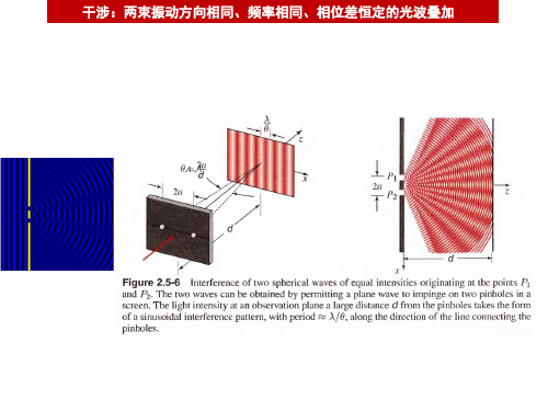
干涉:两束振动方向相同、频率相同、相位差恒定的光波叠加
衍射:波绕过障碍物继续传播,也称绕射
光学成像系统的成像质量或多或少都受到衍射的制约。其原因是,入射光在圆形镜片处会发生衍射,形成艾里斑,从而造成光路不能够汇聚到一个点。 衍射对成像的影响,主要表现为画面细节模糊不清。
惠更斯原理
光波在空间传播,是振动的传播,波在空间各处都引起振动,波场中任一点,即 波前中任一点都可视为新的振动中心,这些振动中心发出的光波,称为次波。 次波又可以产生新的振动中心,继续发出次波,由此使得光波不断向前传播。新 的波面即是这些振动中心发出的各个次波波面的包络面。 用次波的模型可以很容易解释光的衍射现象。 波前上任一点都是一个次波中心,即一个点光源,发出球面波,两个点,即使是 邻近的,发出的次波也是不同的。严格地说,是没有“光线”或“光束”之类的 概念的。
宽频带正方形微带贴片天线的设计_王亚洲

2 i=1
hi
/
L
⎟⎟⎠⎞
−
1 2
(10)
∆L 是贴片的延伸量,由下式求得
∑ ∆L
=
0.412
2 i =1
hi
⎡ε
⎢ ⎣
ε
e
e + 0.3 − 0.258
⎤ ⎥ ⎦
•
⎢⎡⎜⎛
⎟⎞
∑ ⎢⎜
⎢⎜ ⎢⎜ ⎢⎣⎜⎝
L
2
hi
i=1
⎟ + 0.264⎟
⎟ ⎟⎠
⎜⎛
⎟⎞⎥⎤
∑ ⎜
⎜ ⎜ ⎜⎝
L
2
hi
i =1
+ 0.8⎟⎟⎥⎥ ⎟⎥ ⎟⎠⎥⎦
第 22 卷增刊
王亚洲等:宽频带正方形微带贴片天线的设计
31
图 4、图 5 分别是天线在 2.4GHz 和 3.1GHz 时 的远场辐射特性。通常情况下,宽频带天线在高频 时远场方向图容易出现裂瓣,本文设计的宽带天线 在工作频段内方向性基本良好。但是可以看出,随 着工作频率的提高,天线的方向性有变坏的趋势, 因此宽频带天线的高频辐射特性也是以后天线设 计过程中需要不断改进的方面。
42.3% (VSWR ≤ 2 ).
Key words:Broadband, Microstrip patch antenna, Impedance bandwidth
引言
本文介绍了一种新的宽频带微带贴片天线的设 计方法,给出了天线的测量和仿真结果。
微带天线由于具有剖面低、重量轻、成本低, 可与各种载体共形,适合印刷电路板技术批量生 产,便于实现圆极化、双极化、双频段工作等优点, 深受人们的关注,近年来应用也越来越广泛。但微 带天线有其固有缺陷,即阻抗带宽较窄,一般微带 天线的带宽仅有 5%左右[1,2]。微带天线的窄带特性 在很多方面限制了它的广泛应用,因此,展宽微带 天线的带宽具有十分重要的意义。
关于两线圈磁耦合谐振式无线电能传输的效率分析

理论与算法2018.16关于两线圈磁耦合谐振式无线电能传输的效率分析谢端(新疆机场(集团)有限责任公司乌鲁木齐分公司,新疆乌鲁木齐,830016 )摘要:在本次研究通过借助电磁仿真,得出了螺旋线圈在终端开路、短路两种不同的馈电方式下,所得出的相应等效类电路,借助等效电路理论基于螺旋线圈的等效电路,构建了螺旋线圈的终端短路串电容两线圈结构模型。
进一步借助等效电路,得出了系统传输功率及效率的表达公式,分析相应的系统谐振情况下,探宄系统的谐振式无线电能传输功率及效率,发现在最大输出功率情况下,系统的最优互感数值及相应的传输效率,与互感数值之间呈现密切相关性。
关键词:无线电能传输;效率Analysis of the efficiency of the two coil magnetically coupledresonant radio transmissionXie Duan(Xinjiang Airport(Group)Co.,Ltd.Urumqi branch,Urumqi Xinjiang, 830016)Abstract:In this study,by means of electromagnetic simulation,the equivalent equivalent circuitof spiral coil in two different feeding modes of open circuit and short circuit is obtained.By the equivalent circuit theory based on the equivalent circuit of spiral coil,the two coil structure modelof the final short circuit series capacitance of the spiral coil is constructed.With the help of the equivalent circuit,the expression formula of the transmission power and efficiency of the system is obtained.In the case of the corresponding system resonance,the transmission power and efficiencyof the resonant radio can be explored.It is found that under the maximum output power,the optimal mutual inductance value and the transmission efficiency of the phase should be compared with the mutual inductance value.There is a close correlation.K e y w o r d s:radio energy transmission;efficiency1螺旋线圈两种工作方式螺旋线圈的具体馈电点,直接对线圈的不同工作方式造成决定性影响:馈电点所在位置处于线圈中间,即终端开路;馈电点所在位置处于线圈两导线端子上,即终端短路。
CZ和FZ方法介绍以及硅片的生产步骤2
International Scientific ColloquiumModelling for Electromagnetic ProcessingHannover, March 24-26, 2003 Modeling in Industrial Silicon Wafer Manufacturing - From Crystal Growth to Device ProcessesTh. Wetzel, J. VirbulisAbstractSilicon wafer manufacturing is one of the key processes that determine the yield and the profitability in semiconductor device production. The present paper gives an overview on vari-ous applications for numerical modeling in the wafer manufacturing process. It starts with ther-mal and convection models for the crystal growth process, both by the Czochralski (CZ) and the Floating Zone (FZ) method. Within this field, in particular modeling of electromagnetic field influence on melt flow has become an an indispensable means for the puller design and the process development for both methods. A further chapter is devoted to model approaches for predicting crystal defects, like grown-in voids, self-interstitial aggregates or oxygen precipitates. The defect modeling connect the crystal growth directly to the device manufacturing processes, as crystal defects may be detrimental or beneficial to microelectronic devices, produced on the silicon wafer. A last chapter points briefly to more recent applications of numerical modeling in auxiliary processes, like wafer heat treatment steps, epitaxial growth or wafer cleaning.IntroductionDuring the last five decades, the technology for growing silicon monocrystals from the melt, and the subsequent manufacture of silicon wafers, have become highly developed. The quality, purity and size of today's silicon crystals and wafers have reached an outstanding level. However, it remains time consuming and expensive to develop new processes that meet the crystal and wafer quality requirements for devices with further decreasing design rules. The current transition to a wafer diameter of 300 mm creates further challenges for the wafer industry.One of the main driving forces for the use of numerical modeling in the wafer industry are the extremely high costs for growth furnace design and growth process development. Thermal simulation of the global heat transfer in crystal growth furnaces contributes substan-tially to keeping the development costs at an acceptable level. In particular with the transition to 300 mm diameter CZ crystal growth, magnetic fields have become an important additional means to control heat and mass transfer in the large melt volumes. Numerical modeling facilitates the suitable design of inductor systems and helps to understand the effect of the magnetic fields on the melt flow. However, the growth conditions do not only affect yield or pull rate, but also the quality of the crystals. Grown-in defects like voids, self-interstitial aggregates or oxygen precipitates can be detrimental or beneficial in subsequent process steps. Therefore, defect engineering, i.e. the control of the formation of such defects, is an important part of the whole wafer production. Numerical modeling helps to predict the defect formation and behavior through crystal growth and for subsequent process steps, up to the device processes for microelectronic components in the chip manufacturer’s production line.Beside the success of the crystal growth and the defect simulation, there is an increasing number of new applications of numerical modeling in the wafer manufacturing industry, e.g. in process steps like wafer polishing, epitaxial layer growth or wet cleaning of the wafers.1. Crystal GrowthThere are two major methods for producing silicon monocrystals from the melt. With the Czochralski (CZ) method, today crystals of up to 300 mm are grown. The Floating Zone (FZ) technology is currently scaled up to grow 200 mm crystals.1.1 Czochralski GrowthFig. 1 shows a longitudinal cut through a CZ growth furnace. The prediction of the temperature field in the whole furnace and in the crystal requires a global thermal simulation, taking into account the heat transfer byconduction, convection and radiation.Software tools for the conduction andradiation calculation along with the pre-diction of the melt-crystal interface are avai-lable from different institutes [1, 2, 3]. Theyare based on 2D axisymmetric models, em-ploy view factor approaches for theradiation treatment and are based on theFinite Element Method (FEM) or the FiniteVolume Method (FVM). Some of thesecodes allow the reproduction of transientgrowth processes [2].With increasing melt volumes andcrystal diameters, the consideration of themelt convection has become more im-portant. The melt flow in large diameter CZcrucibles - today diameters of up to 32” withloads of up to 450 kg are used - is characte-rized by time dependent, three dimensional processes. The time needed for a fully transient, three-dimensional simulation of melt flow in a crucible of the mentioned size however, still prevents their application for industrial engineering purposes. Therefore,2D axisymmetric steady state models have been developed, that reproduce the most important features of the 3D flow, but do still provide reasonably short calculation time [4, 5]. One of the most critical parts in any CZ melt flow simulation, both 2D and 3D, is the consideration of turbulence. The 2D simulation tools usually employ k-ε or LowRe k-ε or k-ω models. Such tools require careful experimental verification and modification based on comparisons with experiments [5, 6, 7]. A model proposed in [8] provided good agreement of the simulated melt-crystal interface shapes with measured ones for 200 mm crystals. 3D time dependent simulations with LES turbulence models [9] and simulations close to DNS [10, 11] are used to further develop the understanding of the flow behavior and to improve less time consumingsimulation models. One goal of such attempts is the global modeling of oxygen transport in the Fig. 1: Schematic layout of an industrial CZ puller and simulated temperature distribution (left)CZ furnace, which is extremely sensitive towards any lack of precision in the turbulence modeling.Another aspect, closely related to reliable melt flow prediction, is the modeling of magnetic field influence. In 300 mm CZ growth, different types of alternating (AC) magnetic fields as well as static (DC) magnetic fields are used. The incorporation of the melt flow models into the global heat transfer simulation tools facilitates direct consideration of the effect of such fields on the temperature distribution in the crystal and all coupled phenomena, like point defect dynamics. A 2D axisymmetric model approach for the AC and DC magnetic field effect on the silicon melt is described in [5]. The model has been verified with experimental results from a CZ model setup with various magnetic fields [7, 12].1.2 Floating Zone GrowthFig. 2 shows a longitudinal cutthrough an FZ growth setup [13]. For thenumerical simulation of Floating Zonegrowth there is a complete model chainnecessary, starting with the prediction of thephase boundaries at feed rod, molten zoneand crystal, based on RF field influence andheat transfer [14]. A second part of themodel chain is covering the prediction of thetransient melt flow and heat transfer based on2D [15] and 3D [16] approaches. Based onthe melt flow calculation results, the dopanttransport can be simulated, yielding finallythe macroscopic and microscopic resistivitydistributions in grown wafers. The currentdevelopment of 200 mm FZ crystal growthprocesses has been substantially supported bythe use of such simulation models. Beyond these applications, theinfluence of additional low frequency inductors has been modeled [14] and considerations about the stress induced dislocation generation have been started [17]. A recently developed improved phase boundary simulation model is presented in [18].3. Defect ModelingThere are different types of defects in silicon wafers, which are related to the crystal growth conditions and the thermal history of the crystal and wafer. During the solidification process, intrinsic point defects, namely vacancies and silicon self interstitials, are incorporated into the crystal. These intrinsic point defects form grown-in defects during cooling down from melting to room temperature. Impurity atoms can also be incorporated into the growing crystal, later forming precipitates or other defects. The most common of these impurities is oxygen, which is dissolved from the silica crucible in CZ processes and transported through themelt to the crystallization front.Fig. 2: Schematic layout of a Floating Zone setup with simulated features and FEM meshThree types of defects in CZ crystals will bementioned here specifically: grown-in octahedral voids [19]formed by the aggregation of vacancies (Fig. 3), oxideprecipitates [20] and the OSF ring [19].Whether vacancy or self-interstitial related defectsare found in a CZ crystal or crystal region, depends on thevalue v/G in that region at the crystallization interface duringsolidification (v being the pull rate, G the temperaturegradient at the solid/liquid interface) [19, 21]. In addition todetermining these quantities from the thermal simulation,models are used to directly describe the point defectdynamics, i.e. the diffusive and convective transport of thesedefects during crystal growth as well as their annihilation by recombination [22]. The combination of such simulation models with the thermal simulation results, in particular the transient temperature field in the crystal, allows to designthe growth furnace and the growth process in such a way, that grown crystals show a desired defect species.Furthermore, especially for vacancy rich crystals, that are used e.g. for the production of memory chips, it is necessary to ensure a specific size and density of the grown-in voids. Simulation models have been developed, that describe the formation of such defects from vacancies [19]. The size of the grown in voids depends strongly on the cooling rate in a specific temperature interval during cooling down. Therefore, these models do also need the thermal history of the crystal as well as the results of the point defect models. Fig. 4 shows simulated size distributions of voids in fast and slow cooled CZ crystals. The void formation models are also used to predict the impact of wafer heat treatment steps on size and density of the voids.An important part of defect modeling is devoted to the behavior of oxygen in CZ silicon. As oxide precipitates are used as centers for internal gettering [20], models have been developed to predict the size and in particular the density of such defects in CZ crystals and wafers [23]. Another well known defect phenomenon is the so called OSF ring, appearing on the wafer surface afterwet oxidation. Thenature and formationof the OSF ring hasbeen studied by manyauthors (see [19] forfurther ref.). How-ever, there is ongoingresearch activity inthis field, as there arecomplex interactionsof oxygen precipi-tation with other pointdefects or impurityatoms in the growingcrystal, e.g. Nitrogen, that affect e.g. thewidth of the OSF ringFig.3: Octahedral void in anas-grown silicon crystal [19] Fig. 4: Simulated size distributions of voids in crystals with different cooling rates[24].3. Modeling for Wafer Processing StepsFollowing crystal growth, there are several process steps in a wafer production line. It starts with cutting of the ingots, goes through slicing, etching, polishing and ends with final cleaning of the wafers. Inbetween there can be several other steps like lapping, thermal treatment or epitaxial layer growth. In particular in the areas of etching, cleaning and epitaxial layer growth there are several simulation activities based on Computational Fluid Dynamics (CFD) codes, extended with chemistry and mechanical models. Many questions in this field can be handled already with standard CFD tools, like flow distribution in cleaning baths. Other examples for such simulations are the prediction of temperature distributions in annealing furnaces or in RF heated epi reactors.These more recent applications will gain increasing attention as they open a similar potential for improved physical understanding of the processes as well as for saving con-siderable amounts of time and money for process and equipment development. As in the crystal growth and defect modeling activities, the close collaboration of industry and research institutes will be extremely important for such new modeling topics, to finally have them at the same scientific level and with the same impact on industrial day to day research and development work.ConclusionsNumerical modeling is an integral part of today’s industrial silicon crystal growth and wafer manufacturing R&D activities, with a variety of applications. Crystal growth simulation with thermal and convection models, both for the CZ and the FZ method is the most well established application. Within this field, in particular modeling of electromagnetic field influence on melt flow has become an indispensable means for the puller design and the process development for both methods. The defect distribution in a wafer is extremely important for the yield and profitability of microelectronic device production lines. Therefore, various model approaches for predicting crystal growth and wafer treatment related defects, like grown-in voids or oxygen precipitates, have been developed and are successfully used in the industry. New applications of numerical modeling in auxiliary processes, like wafer heat treatment steps, epitaxial growth or wafer cleaning are being developed and successfully used in industrial equipment and process design.References[1] Dornberger, E., Tomzig, E., Seidl, A., Schmitt, S., Leister, H.-J., Schmitt, Ch., Müller, G.: ThermalSimulation of the Czochralski silicon growth process by three different models and comparison with experiment. J. Cryst. Growth 181 (1997), 461 pp.[2] Van den Bogaert, N., Dupret, F.: Dynamic global simulation of the Czochralski process I / II. J. Cryst.Growth 171 (1997), pp. 65-93[3] Kurz, M., Pusztai, A., Müller, G.: Development of a new powerful computer code CrysVUN++ especiallydesigned for fast simulation of bulk crystal growth processes. J. Cryst. Growth (198/199 (1999), pp. 101-106[4] Lipchin, A., Brown, R.A.: Hybrid finite-volume/finite element simulation of heat transfer and turbulence inCzochralski growth of silicon. J. Cryst. Growth 216 (2000), pp. 192-203[5] Wetzel, Th., Muiznieks, A., Mühlbauer, A., Gelfgat, Y., Gorbunov, L., Virbulis, J., Tomzig, E., vonAmmon, W.: Numerical model of turbulent CZ melt flow in the presence of AC and CUSP magnetic fields and its verification in a laboratory facility. J. Cryst. Growth 230 (2001) pp. 81-91[6] Lipchin, A., Brown, R.A.: Comparison of three turbulence models for simulation of melt convection inCzochralski crystal growth of silicon. J. Cryst. Growth 205 (1999) pp. 71-91[7] Krauze, A., Muiznieks, A., Mühlbauer, A., Wetzel, Th., Gorbunov, L., Pedchenko, A.: Numerical 2Dmodeling of turbulent melt flow in CZ system with AC magnetic fields. Proceedings of the Intl. Sc.Colloquium Modelling for Electromagnetic Processing, Hannover, 2003[8] Virbulis, J., Wetzel, Th., Muiznieks, A., Hanna, B., Dornberger, E., Tomzig, E., Mühlbauer, A., vonAmmon, W.: Numerical investigation of silicon melt flow in large diameter CZ-crystal growth under the influence of steady and dynamic magnetic fields. J. Cryst. Growth 230 (2001) pp. 92-99[9] Evstratov, Y., Kalaev, V.V., Zhamakin, A.I., Makarov, Y. N., Abramov, A.G., Ivanov, N.G., Smirnov,E.M., Dornberger, E., Virbulis, J., Tomzig, E., von Ammon, W.: Modeling analysis of unsteady three-dimensional turbulent melt flow during Czochralski growth of Si crystals. J. Cryst. Growth 230 (2001) pp.22-29[10] Vizman, D., Friedrich, J., Müller, G.: Comparison of the predictions from 3D numerical simulation withtemperature distributions measured in Si Czochralski melts under the influence of different magnetic fields.J. Cryst. Growth 230 (2001) pp. 73-80[11] Enger, S., Gräbner, O., Müller, G., Breuer, M., Durst, F.: Comparison of measurements and numericalsimulations of melt convection in Czochralski crystal growth of silicon. J. Cryst. Growth 230 (2001) pp.135-142[12] Pedchenko, A., Gorbunov, L., Gelfgat, Y., et.al.: Investigation of temperature field and melt flows inlarge-diameter CZ silicon modelling experiments with impact of magnetic fields. Proceedings of the Intl.Sc. Colloquium Modelling for Electromagnetic Processing, Hannover, 2003[13] Virbulis, J.: Numerische Simulation der Phasengrenzen und Schmelzenströmung bei der Züchtung vonSiliziumeinkristallen mit dem Floating-Zone Verfahren. Dissertation, Universität Lettlands in Riga 1997 [14] Raming, G.: Modellierung des industriellen FZ-Prozesses zur Züchtung von Silizium-Einkristallen.Dissertation, Institut für Elektrowärme, Universität Hannover 2000[15] Mühlbauer, A.. Muiznieks, A., Virbulis, A., Lüdge, A., Riemann, H.: Interface shape, heat transfer andfluid flow in the floating zone growth of large silicon crystals with the needle-eye technique. J. Cryst.Growth 151 (1995), pp. 66-79[16] Ratnieks, G., Muiznieks, A., Buligins, L., Raming, G., Mühlbauer, A., Lüdge, A., Riemann, H.: Influenceof the three dimensionality of the HF electromagnetic field on resistivity variations in Si single crystals during FZ growth. J. Cryst. Growth 216 (2000), pp. 204-219[17] Muiznieks, A., Raming, G., Mühlbauer, A., Virbulis, J., Hanna, B., v. Ammon, W.: Stress-induceddislocation generation in large FZ- and CZ-silicon single crystals––numerical model and qualitative considerations J. Cryst. Growth 230 (2001) pp. 305-313[18] Ratnieks, G., Muiznieks, A., Mühlbauer, A.: Mathematical modelling of industrial FZ process for large(200mm) silicon crystal growth. Proceedings of the Intl. Sc. Colloquium Modelling for Electromagnetic Processing, Hannover, 2003[19] Dornberger, E.: Prediction of OSF Ring Dynamics and Grown-in Voids in Czochralski Silicon Growth.Dissertation, Universite Catholique de Louvain 1997[20] Gilles, D., Ewe, H.: Gettering phenomena in silicon. Semiconductor Silicon 1994, Electrochemical SocietyProceedings 94-10 (1994) pp. 772[21] Voronkov, V.V.: The mechanism of swirl defects formation in silicon. J. Cryst. Growth 59 (1982) pp. 625-643[22] Sinno, T., Brown, R.A., von Ammon, W., Dornberger, E.: Point Defect Dynamics and the Oxidation-Induced Stacking Fault Ring in Czochralski-Grown Silicon Crystals. J. Electrochem. Soc. 145 (1998) pp.302[23] Esfanyari, J.: Modellierung und Computersimulation der Sauerstoffpräzipitation in Silicium. PhD Thesis,TU Wien 1995[24] von Ammon, W., Hölzl, R., Wetzel, T., Zemke, D., Raming, G., Blietz, M.: Formation of stacking faultsin nitrogen doped silicon single crystals.Proceedings of the 8th International Conference on Electronic Materials, Xian, China 2002AuthorsDr.-Ing. Wetzel, Thomas Dr.-Phys. Virbulis, JanisWacker Siltronic AG Center for Processes’ Analyses Numerical Modeling PAICP.O. Box 1140 Zellu Str. 8D-84479 Burghausen LV-1002 Riga, LatviaE-mail: thomas.wetzel@ E-mail: janis@paic.lv。
Circuital and Numerical Modeling of Electrostatic Discharge Generators
Circuital and Numerical Modeling of Electrostatic Discharge GeneratorsSpartaco CaniggiaITALTEL S.p.A.Settimo Milanese 20019, Milan, ItalyFrancescaromana Maradei Department of Electrical Engineering University of Rome La Sapienza Via Eudossiana 18, 00184 Rome, Italy Francesca.maradei@uniroma1.itAbstract— The paper provides two accurate and efficient models of electrostatic discharge (ESD) generators which permit to reproduce the discharge current in the contact mode taking into account the load effect. The first model is based on a circuit approach and is suitable to be implemented in any commercial circuit simulator. The second model is based on the numerical solution of the field equations by using the commercial numerical code Microwave Studio (MWS) based on the finite integration technique. The validation of the proposed circuit and numerical models is carried out by comparison with measurements. Keywords: Electromagnetic compatibility (EMC), electrostatic discharge (ESD), numerical modeling, immunity.I.I NTRODUCTIONElectrostatic discharge (ESD) generators are widely used for testing the immunity of electronic equipment and permit to reproduce typical human-metal ESD events. To ensure the reproducibility of test results, the majority of available ESD generators are built in compliance with the specifications of the IEC 61 000-4-2 standard and its second edition which is still under discussion [1]. The immunity prediction against ESD events by experimental activity is not considered to be very practical in particular when the evaluations is required for different design choices.For this reason, in the last years a great concern has been addressed by many researches to the numerical simulation of ESD events [2]-[5]. A numerical model based on the FDTD method adopting impedance network boundary conditions was proposed in [2] to predict the ESD effects inside penetrable conductive enclosures. Recently, numerical models based on the finite difference time domain method of typical electrostatic discharge (ESD) generators have been presented in order to simulate current discharge and radiated fields [3], [4]. In the past an analytic approach based on transmission line formulation was proposed to predict voltage induced into a coaxial cable by an ESD discharge [5]. In [5] the ESD was simulated by a current source without taking into account the load effect of the ESD generator. As the same authors recognize, this procedure brings to an overestimation of the subsequent peaks of the induced disturb.The prediction of the immunity by modern software tools based on circuital or numerical approaches requires accurate models for the ESD generator suitable to account for the load effect of the generator.This paper provides two accurate models of the ESD generator that allow modeling the discharge current in the contact mode taking into account the load effect.In the first model the ESD generator is modeled by an electric circuit suitable to be implemented in any commercial circuit simulator.The second model is based on the 3D numerical simulation of the ESD generator by the commercial tool Microwave Studio (MWS) based on the finite integration technique [6].The validation of both the models is made by comparison with the measurements by using the test setup for current calibration reported in [1] and shown in Fig. 1. This test setup models the ESD event on a conductive wall. The flat cable used as ESD strap is connected to the metallic wall where the discharge occurs.Flat cable used as ESD strapconnected to the metallic wallConductive wallMiniZap ESD generatorFigure 1. Test setup used for ESD current calibration.0-7803-9208-6/05/$20.00 (C) 2005 IEEESwitch forchargingSwitch for dischargingI Switch for charging I ESD tipI ESD strapESD gun - boxSwitch fordischargingFigure 2. Spice equivalent circuit of a typical ESD generator.II.M ODEL OF ESD G ENERATORA. Equivalent Circuit ModelThe purpose of an ESD generator is to reproduce typicalhuman-metal ESD. Considering this, a suitable circuital equivalent model could be the one shown in Fig. 2. This circuit model can be easily implemented in any SPICE based circuit simulator [7]. The lumped circuital elements are chosen as typical values that simulate the body and the arm effects of the person that causes ESD. In the circuit model of Fig. 2 there are two switches: the first one (on the left side) is used to charge the 150 pF capacitor at the typical voltage of 5 kV; the second switch (on the right side) provides the discharge. The flat cable used as ESD strap connected to the ground is modeled by the series connection of the lossless transmission line characterized by characteristic impedance 225 Ω and propagation time 3.3 ns, and a 10 nH inductance which models the wire used to connect the flat cable with the metallic wall. The 15 pF capacitance models the capacitive coupling between the ESD gun and the metallic wall (see the experimental setup shown in Fig.1). The ESD tip is modeled by the series of a 25 Ω resistance with the 0.2 µH inductance. It should be noted that the load represents the impedance of the metallic wall, and in the considered simulation is given by a 2 Ω resistance.B. Full-Wave ModelThe ESD generator is modeled by using the commercialnumerical code Microwave Studio (MWS) based on finite integration technique [6]. The model, shown in Fig. 3, contains dielectric parts, metallic parts and lumped circuital elements which permit to reproduce the physical form of a typical ESD generator and the reference discharge current proposed by IEC 77b [1], [3].Dielectric Strap ESD gun Metallic wallDielectricStrapESD gunMetallic wallFigure 3. The ESD simulator modeled in MWS.The geometrical configuration of the ESD generator adopted for the numerical simulation is similar to that of the MiniZap gun. Details on the material properties used to model the different part of the ESD gun are shown in Fig. 4. The lumped circuit elements adopted in the MWS model are shown in Fig. 5. The model is excited at Port 2 (see Fig. 5) by an ideal current source with 25Ω assuming a step rise-time of 1ns to reproduce the actual slow charging, switching and rapid discharge process of an ESD generator.(a)(b)Figure 4. Material details of the ESD simulator model in MWS: perfectelectric conductive (a) and lossy dielectric (b) regions.RL Parallel: R=2 ΩL=1nHPort 2RC Serial: R=50 ΩC=150 pFRC Serial: R=100 ΩC=10 pF RC Parallel: R=330 ΩC=2 pFFigure 5. Lumped element network and port excitation used to reproduce the physical form of a typical ESD generator and the reference discharge currentproposedIII. V ALIDATION OF THE ESD G ENERATOR M ODELS To validate the proposed models, current on the tip and strap of a commercial ESD generator called MiniZap where measured by using the setup for current calibration reported in [1] and shown in Fig. 1. The wall is a side of a shielded enclosure in which a target is mounted to measure currents by an oscilloscope within the enclosure. This configuration permits to avoid the coupling between the ESD event and the instrumentation. All the measurements were carried out at charging voltage of the ESD generator of 5 KV. The experimental setup has been arranged in the shielded room of Italtel S.p.A.The tip and strap current obtained by the two proposed models are shown in Figs 6-7. The comparison between the simulation results and the measurements reveals a very good accuracy. Moreover, the following considerations can be done:0 40 80 120 160 20051015202518283812.250A mp ere18 28 3812.5250C u r r e n t (A )Time (ns)Figure 6. Tip current: measured (solid line); Standard IEC (dot line); SPICE (dashed line); MWS (dashed-dot line).50 100 012.525A mp ereC u r r e n t (A )Time (ns)Figure 7. Strap current: measured (solid line); SPICE (dashed line); MWS (dashed-dot line).• The first fast rise time (less than 1ns) is reproduced and match well with the reference IEC current.•The measured and simulated waveforms after the first peak follow quite well with slight oscillations the reference IEC current. This is mainly due to the length and orientation of the strap.•The current on the strap has slower rise time than the current on the tip. This is due to the capacitance between the ESD generator and the environment (the metallic wall in this case, see the 15pF of Fig.2) that permits an alternative path for the first peak of the ESD current.In order to verify the generality of the developed models in terms of reproducibility of test results even using different ESD gun, the tip current has been measured several time by using the MiniZap gun (Fig. 8a), and by using the DITO gun (Fig. 8b). The measured tip currents shown in Fig.9 show that there is very little difference between two measurements performed with MiniZap gun and with that obtained using DITO gun.(a)(b)Figure 8. ESD generators: MiniZap (a) and DITO (b) guns.5010012.525A mp ere Time (ns)C u r r e n t (A )Figure 9. Measured tip current: MiniZap (solid line); MiniZap 2 (dot line); Dito (dashed line).IV.C ONCLUSIONCircuit and numerical models of the ESD generator have been proposed and discussed. The circuit model is suitable to be implemented in any commercial circuit simulator such as SPICE. The numerical model is based on the 3D simulation by the commercial tool MWS based on the finite integration technique. Both the models allow the accurate simulation of the discharge current in the contact mode taking into account the load effect. The comparison of the simulation results with measurements have revealed a very good accuracy.The proposed models are of great interest since they represent an important item in the development of software tools suitable for the prediction of ESD immunity, especially during the design stage.A CKNOWLEDGMENTThe research has been financially supported by Italtel S.p.A.R EFERENCES[1]77B/378/CDV, “IEC 61000-4-2: EMC-Part 4-2: testing andmeasurement techniques- ESD immunity test”, 2003-04-11.[2] F. Maradei, M. Raugi, “Analysis of upset and failures due to ESD by theFDTD-INBCs method”, IEEE Trans. Industry Applications, vol. 38, no.4, Jul./Aug.2002, pp.1009-1017, James Melcher Price Paper Award. [3]Kai Wang, D. Pommerenke, R. Chundru, T. Van Doren, J. Drewniak, A.Shashindranath, “Numerical Modeling of Electrostatic Discharge Generators“, IEEE Trans. on EMC, vol.45, no.2, May 2003.[4]S. Caniggia, F. Centola, D. Pommerenke, Kai Wang, T. Van Doren,“ESD Excitation Model for Susceptibility Study”, IEEE EMC Symp., Boston, 18-22 Aug. 2003.[5]G. Cerri, R. De Leo, V. Mariani Primiani, “ESD Indirect CouplingModeling“, IEEE Trans. on EMC, vol.38, no.3, August 1996.[6]Microwave Studio, Computer Simulation Technology (CST),www.cst.de[7]Spectrum Software, 1021 S. Wolfe Road Sunnyvale, CA 94086,。
电快速瞬变脉冲群发生器耦合方式
电快速瞬变脉冲群发生器耦合方式The coupling methods of electrical fast transient burst generators refer to the various techniques used to couple the generated transient pulses into the device or system under test. These coupling methods are crucial for accurately simulating thereal-world electromagnetic interference conditions that the device may encounter during its operational life. The choice of the appropriate coupling method depends on the nature of the test, the characteristics of the device under test, and the desired test objectives.电快速瞬变脉冲群发生器的耦合方式指的是将产生的瞬态脉冲耦合到待测设备或系统中的各种技术。
这些耦合方式对于准确模拟设备在其使用寿命期间可能遇到的实际电磁干扰条件至关重要。
选择合适的耦合方式取决于测试的性质、待测设备的特性以及期望的测试目标。
One common coupling method is direct coupling, where the generator is directly connected to the input or output terminals of the device under test. This method provides a high-efficiency transfer of the transient pulses and is suitable for testing the device's response to direct electromagnetic interference. However, it may not be suitable for all devices, as some may be sensitive to the direct connection of external sources.一种常见的耦合方式是直接耦合,即发生器直接连接到待测设备的输入或输出端。
深海拖曳式瞬变电磁的响应规律
深海拖曳式瞬变电磁的响应规律周胜;席振铢;宋刚;李波;左立标;侯海涛【摘要】By analyzing the electrical characteristics of the deep-sea hydrothermal sulfide ores, an electrical model was established. The transient electromagnetic (TEM) response to the model was computed according to the theory of the TEM response in full-space, which provided a basis for the deep-sea towed TEM system. The results show that the TEM responses to models in deep-sea are similar in the curve shape to that on the earthground, while the amplitude increases significantly. The towing height seriously reduces the TEM response to the mineralized low-resistivity layer. The abnormal response delays and decreases rapidly when the towing height increases. It is difficult to distinguish the response when the height is more than 50 m. Generally, it is possible to distinguish the response to the mineralized low-resistivity layer within 1-100 m window.%通过分析深海堆积型热液硫化矿的电性特征,建立探测深海热液金属硫化物矿床地电模型:运用瞬变电磁全空间理论计算方法,模拟计算深海热液金属硫化物矿床瞬变电磁响应,为设计深海拖曳式瞬变电磁系统提供依据.计算结果表明:深海与无海水情况下的瞬变电磁相比,响应曲线形态变化不大,响应幅值显著增加;拖曳高度严重降低了低阻矿化层的瞬变电磁响应幅值:随着拖曳高度的增加,低阻矿化层的异常响应向后延迟并迅速衰减,当拖曳高度超过50 m时异常响应将难以分辨;在一般情况下,在1~100 ms时窗内可以探测到海底金属硫化矿层引起的异常.【期刊名称】《中南大学学报(自然科学版)》【年(卷),期】2012(043)002【总页数】6页(P605-610)【关键词】拖曳式瞬变电磁;深海热液硫化矿;拖曳高度;观测时窗【作者】周胜;席振铢;宋刚;李波;左立标;侯海涛【作者单位】中南大学地球科学与信息物理学院,湖南长沙,410083;长沙五维地科勘查技术有限责任公司,湖南长沙,410205;中南大学地球科学与信息物理学院,湖南长沙,410083;长沙五维地科勘查技术有限责任公司,湖南长沙,410205;北京先驱高科技开发公司,北京,100081;北京先驱高科技开发公司,北京,100081;长沙五维地科勘查技术有限责任公司,湖南长沙,410205【正文语种】中文【中图分类】P319.1+2海底热液硫化物矿是继发现锰结核后的又一种海底矿产资源,赋存于水深1.2~3.7 km的热液活动区,富含Cu,Zn,Pb,Ag,Au,Co,Cd和Mn等金属,主要分布在环太平洋构造带中的西太平洋,以及西南太平洋的弧后扩张盆地、东太平洋海隆和大西洋洋中脊区域,堆积在长度为数百米、宽度为近百米的范围内,品位高、埋深浅,资源开发前景广阔,已成为各国海洋资源调查的重点之一[1]。
- 1、下载文档前请自行甄别文档内容的完整性,平台不提供额外的编辑、内容补充、找答案等附加服务。
- 2、"仅部分预览"的文档,不可在线预览部分如存在完整性等问题,可反馈申请退款(可完整预览的文档不适用该条件!)。
- 3、如文档侵犯您的权益,请联系客服反馈,我们会尽快为您处理(人工客服工作时间:9:00-18:30)。
特种铸造及有色合金 2008 年年会专刊
Coupled Modeling of Electr oma gnet ic Flel d , Fluid Flo w, Hea t Transfer and Sol idif ica t ion Dur in g Con vent ional DC Ca st ing an d Low Ftequency Electrmagnetic Casting of 7xxx Aluminum Alloys
中图分类号 T G146. 2 + 1 文献标志码 A 文章编号 2008( s) - 0485n
The al umi num indust ry p roduces ext rusion bill et s and rolling2sheet i ngot s mai nly by t he direct2chill (DC) ca sti ng process . Di rect chill casti ng is a semi2 conti nuous process i n which mol ten al uminum alloy entering t he t op of a wate r2cooled mol d , i s coole d , and for ms a soli d billet draw n out below . In t he past fif ty
Zhang Hai tao1 , Naga um Hi romi2 , Zuo Yubo 1 , Cui J i anZhong1 ( 1. Key Lab. of Elect ro magnetic Processi ng of M at erial s , Mi nist ry of Education , Nort hea ster n Univer si t y 2. Nippon Li ght M et al Company L t d. , Ni kkei Research and Development Center , 123421 Ka mbara Ka mbara2cho , Ihara2gun , Shizuo ka2ken 42123291 , J apan a Email : hai tao_zha ng77 @hot mail. com) Abstract : A co mprehensive mat hematical model has been developed to descri be t he i nt eraction of t he mult ipl e p hysics fiel ds duri ng t he conventional DC casti ng and L FEC ( low f requency elect romagnetic casti ng) process . The model is based on a com binat ion of t he commercial finit e ele ment package A NS YS and t he com me rcial fi nit e vol ume package FLU EN T , wit h t he former for t he calculation of t he elect ro2 magnetic fiel d and t he lat ter for t he cal culation of t he magnet ic dri ven fl uid flow , heat t ra nsfer and soli d2 ification. Moreover , t he model has bee n verified agai nst t he t emperat ure mea sureme nt s obt ai ned from t wo 7XXX al uminum alloy bill et s of 200m m diameter , cast during t he conventional DC ca sting and t he L F EC cast ing proces ses. In addition , a measure ment of t he sump s hape of t he billet s were carried out by using a ddition mel ting met al of Al230 %Cu alloy i nto t he bil let s during cast ing proce ss. There was a good agreement bet ween t he calculat ed re sult s a nd t he measured res ult s . F urt her , comparison of t he calculat2 ed resul t s duri ng t he L F EC proce ss wit h t hat during t he convent io nal DC casti ng proces s indicat ed t hat velocit y pat terns , t emperat ure profiles and t he sump dept h are st rongl y modifie d by t he application of a low f requency el ect romagnetic fi el d duri ng t he DC casti ng. Key words :low f requency elect ro magnetic ca sting ; DC casti ng ; coupl ed modeli ng ; temperat ure field ; fl u2 id flow ; solidification.