HX3141 DC-DC升压IC
canon eos m5中文使用手册说明书
基本指南進階指南相機的基本操作自動模式/混合自動拍攝模式其他拍攝模式播放模式無線功能設定選單配件附錄索引P 模式Tv 、Av 、M 、C1及C2模式用前須知基本指南進階指南相機的基本操作自動模式/混合自動拍攝模式其他拍攝模式播放模式無線功能設定選單配件附錄索引P 模式Tv 、Av 、M 、C1及C2模式用前須知基本指南進階指南相機的基本操作自動模式/混合自動拍攝模式其他拍攝模式播放模式無線功能設定選單配件附錄索引P 模式Tv 、Av 、M 、C1及C2模式用前須知基本指南進階指南相機的基本操作自動模式/混合自動拍攝模式其他拍攝模式播放模式無線功能設定選單配件附錄索引P 模式Tv 、Av 、M 、C1及C2模式用前須知2223232424262728293131 (33)34 (37) (37)37基本指南進階指南相機的基本操作自動模式/混合自動拍攝模式其他拍攝模式播放模式無線功能設定選單配件附錄索引P 模式Tv 、Av 、M 、C1及C2模式用前須知5353 (53)5556) (56)) (57)5858) (58)) (59)) (59)) (59)) (60)(以1分鐘的短片為例) (60)) (61)61 (62)63636464656566) (66)在混合自動拍攝模式下拍攝 .播放短片摘要靜止影像/短片靜止影像短片場景圖示 .螢幕上的方框 ......................................................................................常用的便捷功能 ...............................................................................42使用自拍 ..............................................................................................使用自拍功能以避免相機震動 .....................................................自訂自拍 .........................................................................................輕觸螢幕進行拍攝(輕觸式快門) .......................................................連續拍攝 ..............................................................................................影像自訂功能 ...................................................................................45變更影像畫質 ......................................................................................拍攝RAW 格式的影像 ....................................................................使用選單 .........................................................................................變更長寬比 ..........................................................................................變更短片影像畫質 ..............................................................................實用的拍攝功能 ...............................................................................48使用雙軸電子水平儀 ..........................................................................使用自動程度 ......................................................................................自訂相機操作 ...................................................................................49避免自動對焦輔助光發光 ..................................................................關閉防紅眼燈 ......................................................................................變更拍攝後影像的顯示時間 ..............................................................其他拍攝模式.....................................................................使用您喜愛的設定進行拍攝(創意輔助儲存/載入設定.儲存設定載入設定基本指南進階指南相機的基本操作自動模式/混合自動拍攝模式其他拍攝模式播放模式無線功能設定選單配件附錄索引P 模式Tv 、Av 、M 、C1及C2模式用前須知8181818182828283 (83)84 (84)85858686 (87)8889) (89) (91)929292 (93).............................93調整影像亮度(曝光補償關閉曝光模擬鎖定影像亮度/曝光(自動曝光鎖變更測光方法 .變更ISO 感光度調整自動ISO 設定 .自動包圍曝光(自動包圍曝光拍攝) ...................................................自動校正亮度及對比度(自動亮度優化) ...........................................拍攝明亮主體(高光色調優先) ...........................................................影像色彩 ...........................................................................................71調整白平衡 ..........................................................................................自訂白平衡 .....................................................................................手動校正白平衡 .............................................................................手動設定白平衡色溫 .....................................................................自訂色彩(相片風格) ...........................................................................自訂相片風格 .................................................................................儲存自訂相片風格 .........................................................................對焦 ...................................................................................................75選擇自動對焦方式 ..............................................................................單點自動對焦 .................................................................................+追蹤............................................................................................流暢區域自動對焦 .........................................................................選擇要對焦的主體(觸控自動對焦使用自動對焦鎖拍攝 ..........................................................................使用伺服自動對焦拍攝 ......................................................................變更對焦設定 ......................................................................................微調焦點 ..............................................................................................使用手動對焦模式拍攝 .輕鬆辨識對焦區域(手動對焦突出輪廓) .閃光燈 ...............................................................................................80變更閃燈模式 .自動 .................................................................................................基本指南進階指南相機的基本操作自動模式/混合自動拍攝模式其他拍攝模式播放模式無線功能設定選單配件附錄索引P 模式Tv 、Av 、M 、C1及C2模式107108108109109110110110111111111111112112113113114115115116117117119120120將功能指定給按鈕及轉盤將功能指定給速控轉盤自訂快速設定選單 .選擇要包含在選單中的項目重新排列選單項目儲存拍攝設定 ......................................................................................可儲存的設定 .................................................................................儲存常用拍攝選單項目(我的選單) ...................................................重新命名我的選單設定頁 .............................................................刪除我的選單設定頁 .....................................................................將我的選單設定頁或項目全部刪除 .............................................自訂我的選單設定頁顯示 .............................................................播放模式..........................................................................檢視 .................................................................................................100輕觸式螢幕操作 ................................................................................切換顯示模式 ....................................................................................自訂顯示的拍攝資訊 ...................................................................過度曝光警告(影像的光亮部份) .顯示自動對焦點 ...........................................................................顯示格線 .......................................................................................亮度直方圖 ...................................................................................RGB 直方圖 ...................................................................................拍攝靜止影像時檢視建立的短片按日期檢視 ...................................................................................瀏覽及篩選影像 .............................................................................104使用索引搜尋影像 .輕觸式螢幕操作輕觸兩下放大尋找符合特定條件的影像 .使用主轉盤在影像之間跳轉 .輕觸式螢幕操作基本指南進階指南相機的基本操作自動模式/混合自動拍攝模式其他拍攝模式播放模式無線功能設定選單配件附錄索引P 模式Tv 、Av 、M 、C1及C2模式141141142142142143發送的影像 ........................143 .............................144 ................................................144144144145146146147 ...................................................147148 ............................................................148 ....................................................149150150150151151152152152縮減檔案大小 .編輯短片摘要 .無線功能.可用的無線功能使用Wi-Fi 功能使用藍牙®功能 ..................................................................................將影像傳輸至智能手機 .................................................................124將影像傳輸至具備藍牙功能的智能手機 ........................................將影像傳輸至兼容NFC 的智能手機 ................................................相機處於拍攝模式時透過NFC 連接............................................相機處於播放模式時透過NFC 連接............................................透過Wi-Fi 選單連接至智能手機.......................................................使用其他存取點 ................................................................................確認存取點的兼容性 ...................................................................使用兼容WPS 的存取點 ...............................................................連接至列出的存取點 ...................................................................以前使用過的存取點 ...................................................................發送影像至註冊的網絡服務 .........................................................132註冊網絡服務 ....................................................................................註冊CANON iMAGE GATEWAY ...............................................註冊其他網絡服務 .......................................................................上傳影像至網絡服務 ........................................................................使用媒體播放器檢視影像 .............................................................136從連接的打印機無線打印影像 .....................................................137發送影像至其他相機影像發送選項發送多張影像 .逐張選擇影像選擇範圍發送評分的影像基本指南進階指南相機的基本操作自動模式/混合自動拍攝模式其他拍攝模式播放模式無線功能設定選單配件附錄索引P 模式Tv 、Av 、M 、C1及C2模式用前須知164164165166166166167167 (169169169)170171171171171172173174 ...........................................174175175175176176176 ...........................................................177 ...........................................177 .. (177)使用省電模式 .省電調整 .螢幕亮度 .切換螢幕資訊顏色 .世界時鐘 .日期及時間 .顯示的語言 ........................................................................................關閉相機聲音 ....................................................................................開啟相機聲音 ....................................................................................隱藏提示 ............................................................................................按圖示列出拍攝模式 ........................................................................調整輕觸式螢幕面板 ........................................................................清潔影像感應器 ................................................................................關閉自動清潔 ...............................................................................啟動清潔感應器 ...........................................................................手動清潔感應器 ...........................................................................查看認證標誌 ....................................................................................設定要記錄在影像中的版權資訊 ....................................................刪除全部版權資訊 .......................................................................調整其他設定 ....................................................................................回復相機的預設設定 ........................................................................回復相機的所有預設值 ...............................................................回復個別功能的預設值 ...............................................................配件 .................................................................................系統圖 .............................................................................................161另購配件 .. (162)鏡頭 ....................................................................................................電源 ....................................................................................................閃光燈 ................................................................................................麥克風 ................................................................................................其他配件 ............................................................................................打印機 ................................................................................................基本指南進階指南相機的基本操作自動模式/混合自動拍攝模式其他拍攝模式播放模式無線功能設定選單配件附錄索引P 模式Tv 、Av 、M 、C1及C2模式用前須知清除打印清單的所有影像將影像加入相簿 .指定選擇的方法逐張加入影像將所有影像加入相簿移除相簿的所有影像附錄 .................................................................................疑難排解 .........................................................................................179螢幕提示 .........................................................................................183螢幕資訊 .. (185)拍攝時 ................................................................................................電量 ...............................................................................................播放時 ................................................................................................資訊顯示1 .....................................................................................資訊顯示2 .....................................................................................資訊顯示3 .....................................................................................資訊顯示4 .....................................................................................資訊顯示5 .....................................................................................資訊顯示6 .....................................................................................資訊顯示7 .....................................................................................資訊顯示8 .....................................................................................短片控制介面的總覽 ...................................................................功能及選單表 (188)各拍攝模式下的可用功能 ................................................................快速設定選單 ....................................................................................拍攝設定頁 .C.Fn 設定頁INFO.速控.設定設定頁 .我的選單設定頁 .播放設定頁 .播放模式下的快速設定選單 .206206206206206207207207207208209209210210210210210210211)的注意事項 ...............................214214214215 . (215215215)基本指南進階指南相機的基本操作自動模式/混合自動拍攝模式其他拍攝模式播放模式無線功能設定選單配件附錄索引P 模式Tv 、Av 、M 、C1及C2模式用前須知基本指南進階指南相機的基本操作自動模式/混合自動拍攝模式其他拍攝模式播放模式無線功能設定選單配件附錄索引P 模式Tv 、Av 、M 、C1及C2模式用前須知基本指南進階指南相機的基本操作自動模式/混合自動拍攝模式其他拍攝模式播放模式無線功能設定選單配件附錄索引P 模式Tv 、Av 、M 、C1及C2模式用前須知用前須知基本指南進階指南相機的基本操作自動模式/混合自動拍攝模式其他拍攝模式播放模式無線功能設定選單配件附錄索引P 模式Tv 、Av 、M 、C1及C2模式用前須知基本指南進階指南相機的基本操作自動模式/混合自動拍攝模式其他拍攝模式播放模式無線功能設定選單配件附錄索引P 模式Tv 、Av 、M 、C1及C2模式用前須知基本指南進階指南相機的基本操作自動模式/混合自動拍攝模式其他拍攝模式播放模式無線功能設定選單配件附錄索引P 模式Tv 、Av 、M 、C1及C2模式用前須知基本指南進階指南相機的基本操作自動模式/混合自動拍攝模式其他拍攝模式播放模式無線功能設定選單配件附錄索引P 模式Tv 、Av 、M 、C1及C2模式用前須知基本指南進階指南相機的基本操作自動模式/混合自動拍攝模式其他拍攝模式播放模式無線功能設定選單配件附錄索引P 模式Tv 、Av 、M 、C1及C2模式用前須知基本指南進階指南相機的基本操作自動模式/混合自動拍攝模式其他拍攝模式播放模式無線功能設定選單配件附錄索引P 模式Tv 、Av 、M 、C1及C2模式用前須知基本指南進階指南相機的基本操作自動模式/混合自動拍攝模式其他拍攝模式播放模式無線功能設定選單配件附錄索引P 模式Tv 、Av 、M 、C1及C2模式用前須知基本指南進階指南相機的基本操作自動模式/混合自動拍攝模式其他拍攝模式播放模式無線功能設定選單配件附錄索引P 模式Tv 、Av 、M 、C1及C2模式用前須知基本指南進階指南相機的基本操作自動模式/混合自動拍攝模式其他拍攝模式播放模式無線功能設定選單配件附錄索引P 模式Tv 、Av 、M 、C1及C2模式用前須知基本指南進階指南相機的基本操作自動模式/混合自動拍攝模式其他拍攝模式播放模式無線功能設定選單配件附錄索引P 模式Tv 、Av 、M 、C1及C2模式升起閃光燈],請按下起閃光燈。
EG1192L DC-DC电源芯片数据手册说明书
电源输入端
测试条件
-
最小
-0.3
最大
100
单位
V
EN
使能脚
-
输入电源电阻比例分
VIA
-
压后输出
FB
电压反馈输入
-
-0.3
7
V
-0.3
7
V
-0.3
7
V
VB
悬浮电源
-
VS-0.3 VS+7V
V
VS
悬浮地
-
MOS 峰值电流保护输
IS
-
入端口
TA
环境温度
-
-0.3
100
V
VS-0.3 VS+6V
V
-45
125
悬浮 驱动
VREF=0.18V
比较器 图 5-1. EG1192L 内部电路图
6 VB 1 VIN 7 VS 8 IS
2021 ©屹晶微电子有限公司 版权所有
3/8
屹晶微电子有限公司
6. 典型应用电路
EG1192L 芯片数据手册 V1.0
零功耗使能降压 DCDC 电源芯片
图 6-4. EG1192L 快充方案典型应用图
2021 ©屹晶微电子有限公司 版权所有
5/8
屹晶微电子有限公司
7. 电气特性
EG1192L 芯片数据手册 V1.0
零功耗使能降压 DCDC 电源芯片
7.1 最大额定值
无另外说明,在 TA=25℃条件下
符号
参数名称
VIN
2021 ©屹晶微电子有限公司 版权所有
1/1
屹晶微电子有限公司
EG1192L 芯片数据手册 V1.0
XL6019芯龙(XLSEMI)一级代理推荐升压型直流电源变换器芯片
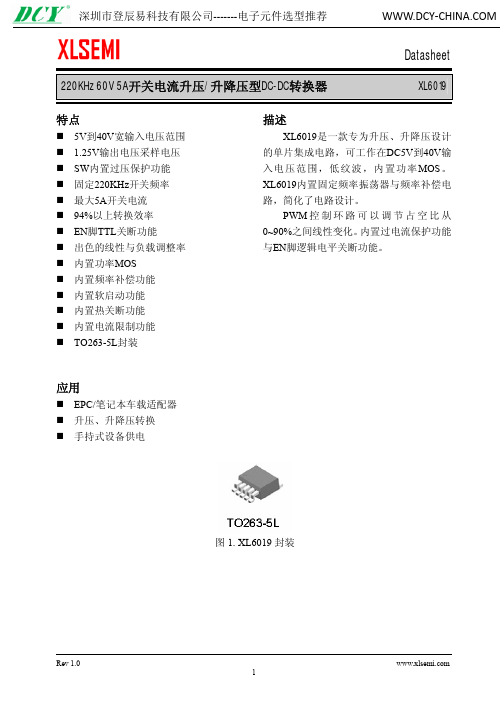
220KHz 60V 5A 开关电流升压/升降压型DC-DC 转换器 XL6019特点5V 到40V 宽输入电压范围 1.25V 输出电压采样电压 SW 内置过压保护功能固定220KHz 开关频率 最大5A 开关电流 94%以上转换效率 EN 脚TTL 关断功能 出色的线性与负载调整率 内置功率MOS 内置频率补偿功能 内置软启动功能 内置热关断功能 内置电流限制功能 TO263-5L 封装应用EPC/笔记本车载适配器 升压、升降压转换 手持式设备供电描述XL6019是一款专为升压、升降压设计的单片集成电路,可工作在DC5V 到40V 输入电压范围,低纹波,内置功率MOS 。
XL6019内置固定频率振荡器与频率补偿电路,简化了电路设计。
PWM 控制环路可以调节占空比从0~90%之间线性变化。
内置过电流保护功能与EN 脚逻辑电平关断功能。
图1. XL6019封装220KHz 60V 5A开关电流升压/升降压型DC-DC转换器XL6019220KHz 60V 5A开关电流升压/升降压型DC-DC转换器XL6019图3. XL6019方框图220KHz 60V 5A开关电流升压/升降压型DC-DC转换器XL6019220KHz 60V 5A开关电流升压/升降压型DC-DC转换器XL6019220KHz 60V 5A开关电流升压/升降压型DC-DC转换器XL6019220KHz 60V 5A开关电流升压/升降压型DC-DC转换器XL6019220KHz 60V 5A开关电流升压/升降压型DC-DC转换器XL6019系统参数测量电路(VIN=5V,VOUT=12V)220KHz 60V 5A开关电流升压/升降压型DC-DC转换器XL6019系统参数测量电路(VIN=10~32V,VOUT=36VEfficiency VS Output current220KHz 60V 5A开关电流升压/升降压型DC-DC转换器XL6019220KHz 60V 5A开关电流升压/升降压型DC-DC转换器XL6019图17. XL6019典型系统应用(SEPIC VIN=10~30V220KHz 60V 5A开关电流升压/升降压型DC-DC转换器XL6019220KHz 60V 5A开关电流升压/升降压型DC-DC转换器XL6019重要申明XLSEMI保留在任何时间、在没有任何通报的前提下,对所提供的产品和服务进行更正、修改、增强的权利。
dc升压芯片
dc升压芯片DC升压芯片是一种将直流电压升高的电子元件,被广泛应用于各种电源供应系统中。
在这篇文章中,我将介绍DC升压芯片的原理、特点和应用领域。
首先,我们来看一下DC升压芯片的原理。
DC升压芯片通过控制开关管的开关状态,实现对输入电压进行变换。
通常情况下,DC升压芯片采用开关型稳压技术,即将输入电压通过开关管控制在一定的占空比下,通过电感储能并通过输出电容进行平滑,从而达到升压的效果。
DC升压芯片的特点之一是高效率。
由于开关型稳压技术的特点,DC升压芯片可以实现高效率的升压转换。
相对于线性升压电路,DC升压芯片的效率更高,能够更好地满足工程设计对能源的管理需求。
其次,DC升压芯片的特点之二是可调性。
DC升压芯片可以通过调整输入输出电压比,实现对电压的精确控制。
这种可调性使得DC升压芯片在许多应用中非常有用,例如太阳能充电器、燃料电池电源和LED照明等。
除了高效率和可调性,DC升压芯片还具有其他一些特点。
例如,DC升压芯片通常具有较低的电磁干扰(EMI)和较高的抗干扰能力。
这些特点使得DC升压芯片在电磁环境较恶劣的设备中更加稳定可靠。
在实际应用中,DC升压芯片有着广泛的应用领域。
首先是电子产品领域,例如移动设备和便携式电子设备,它们通常需要一个输出电压比输入电压高的电源系统,以满足电路的要求。
其次是新能源领域,例如太阳能、风能和燃料电池等,这些能源系统的输出电压往往需要经过升压转换才能应用于实际设备。
此外,DC升压芯片还可以用于LED照明和汽车电子等领域。
总结一下,DC升压芯片是一种将直流电压升高的电子元件,通过控制开关管的开关状态实现对输入电压的变换。
它具有高效率、可调性和抗干扰能力强的特点,被广泛应用于电子产品和新能源领域。
XT1861_C南麟小电流低功耗DC-DC升压IC
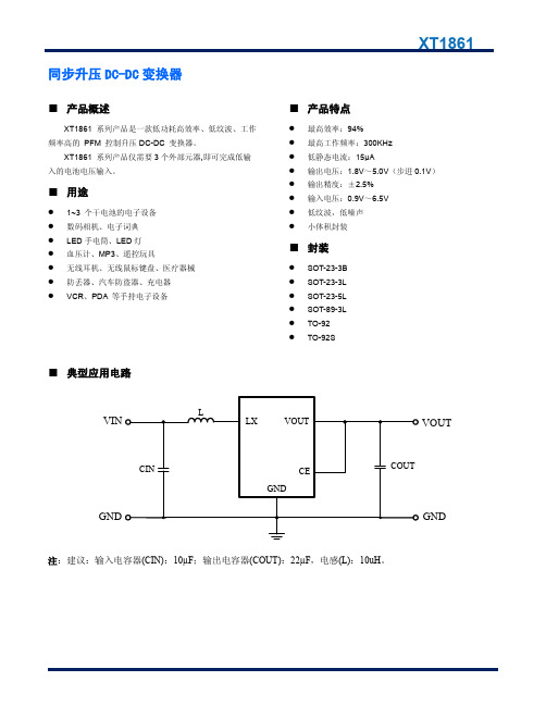
同步升压DC-DC 变换器■ 产品概述XT1861 系列产品是一款低功耗高效率、低纹波、工作频率高的 PFM 控制升压DC-DC 变换器。
XT1861 系列产品仅需要3个外部元器,即可完成低输入的电池电压输入。
■ 用途● 1~3 个干电池的电子设备 ● 数码相机、电子词典 ● LED 手电筒、LED 灯 ● 血压计、MP3、遥控玩具● 无线耳机、无线鼠标键盘、医疗器械 ● 防丢器、汽车防盗器、充电器 ●VCR 、PDA 等手持电子设备■ 产品特点● 最高效率:94% ● 最高工作频率:300KHz ● 低静态电流:15µA● 输出电压:1.8V ~5.0V (步进0.1V ) ● 输出精度:±2.5% ● 输入电压:0.9V ~6.5V ● 低纹波,低噪声 ●小体积封装■ 封装● SOT-23-3B ● SOT-23-3L ● SOT-23-5L● SOT-89-3L ● TO-92 ●TO-92S■ 典型应用电路VINGNDGND VOUT注:建议:输入电容器(CIN):10µF ;输出电容器(COUT):22µF ,电感(L):10uH 。
■ 订购信息XT1861 B ①②③④⑤■ 引脚配置CE VOUT NC LXSOT-23-5L (TOP VIEW)GNDGND VOUTLX SOT-23-3L (TOP VIEW)GND VOUT LX SOT-89-3L (TOP VIEW)TO-92(FRONT VIEW)GND VOUT LXTO-92S (FRONT VIEW)GND VOUT LX12312345123123123■ 引脚分配■ 打印信息SOT-23-3L/B, SOT-23-5L, SOT-89-3L, TO-92, TO-92SSOT-89-3L (TOP VIEW)TO-92(FRONT VIEW)① ② ③ ④......SOT-23-5L (TOP VIEW)SOT-23-3L (TOP VIEW)① ② ③ ④......① ② ③ ④......① ② ③ ④......TO-92S (FRONT VIEW)①②③④......① 表示产品系列② 代表输出电压范围③ 代表输出电压④ 代表生产批号数字0-9,A-Z ,倒写数字0-9,A-Z ,然后重复(G ,I ,J ,O ,Q ,W 除外) 例如:A6TX ,代表XT1861B552*R ,输出电压5.5V 。
注塑机用超级单元_大金_-说明书
2.2.1 主规格............................................................................................................................................ 2-3 2.2.2 性能规格 ....................................................................................................................................... 2-5
2.2 规格 ....................................................................................................................................................... 2-3
5.2 接线 ............................................................................................................................ 5-3 5.3 周边机器的选定 .............................................................................................................................. 5-4
无电感5伏输出电荷泵型降压DCDC芯片
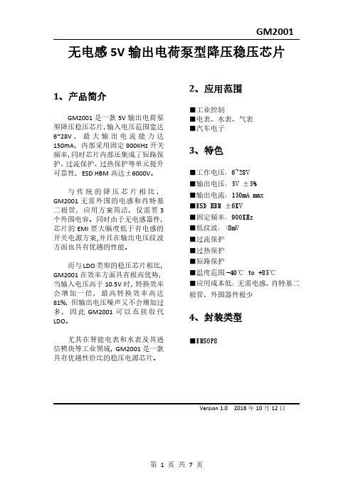
GM2001无电感5V输出电荷泵型降压稳压芯片1、产品简介GM2001是一款5V输出电荷泵型降压稳压芯片,输入电压范围宽达6~28V,最大输出电流能力达150mA,内部采用固定900KHz开关频率,同时芯片内部还集成了短路保护、过流保护、过热保护等单元提升可靠性,ESD HBM高达±6000V。
与传统的降压芯片相比,GM2001无需外围的电感和肖特基二极管,应用方案简洁,仅需要3个外围电容。
同时由于无电感器件,芯片的EMI要大幅度低于有电感的开关电源方案,并且在输出电压纹波方面也具有优越的性能。
而与LDO类型的稳压芯片相比,GM2001在效率方面具有极高优势,当输入电压高于10.5V时,转换效率会增加一倍,最高转换效率高达81%,但输出电压噪声又不会增加过多,因此GM2001可以直接取代LDO。
尤其在智能电表和水表及其通信模块等工业领域,GM2001是一款具有优越性价比的稳压电源芯片。
2、应用范围■工业控制■电表、水表、气表■汽车电子3、特色■工作电压:6~28V■输出电压:5V±5%■输出电流:150mA max■ESD HBM±6KV■固定频率:900KHz■低纹波:<8mV■过流保护■过热保护■短路保护■温度范围-40℃to+85℃■应用成本低:无需电感、肖特基二极管、外围器件极少4、封装类型■EMSOP85、功能引脚定义图1、GM2001Top View 序号名称说明1VIN输入引脚2NC3GND接地4CP飞电容正端5CN飞电容负端6NC7NC8VOUT输出引脚注意:EP必须在PCB设计时接露铜散热区6、典型应用电路图2典型应用电路图7、极限参数符号说明大小单位VCC最大输入端电压30VTj最大结温170℃Θja热阻40℃/W Tstg储存温度-60~160℃Pd最大消耗功率(ESOP8) 1.5WESD HBM6000V8、电气特性(各外围参数如图2所示,VDD=12V,TA=+25℃,除非特别注明)参数符号条件最小典型最大单位输入电压VCC628V输出电压VOUT VCC:7~28V 4.75 5.3V电压精度△Vout±5%静态电流Iin空载 1.1mA输出电流Iout100150mA负载调整Vrl负载电流0~100mA 3.7mV/mA 负载电流50~100mA1mV/mA 输入调整Vri VCC:7~28V1mV/V 开关频率Fosc900KHz电源抑制PSRR1Hz~10Mhz50dB输出纹波Riple负载电流=100mA57mV负载电流=15mA1mV短路电流Ishort输出短路到地22mA过流保护Ip200mA热保护点Tp150℃Thys20℃热保护迟滞9、典型特性图3、转换效率VS.输入电压(Iout=100mA)图4、转换效率VS.输出电流(VIN=12V)图5、输入端纹波(Iout=100mA)图6、输出端纹波(Iout=100mA)图7、负载响应CH1:Iout25mA/Div CH2:Vout20mV/Div100us/Div图8、输入响应图9、开关频率VS.温度图10、电源抑制比图11、输出纹波频谱(Iout=100mA)图12、输出纹波频谱(Iout=10mA)10、应用说明概述GM2001是一款电荷泵降压型稳压芯片,可以提供稳定的5V输出,最大输出电流能力达150mA。
松下汽车系统方案 (信息娱乐篇)

Codec
Audio Codec (MP3 / WMA / AAC)
Other
Audio IN : IIS × 8、SPDIF × 2ch、ADC × 4ch Audio OUT : IIS × 4、DAC × 6ch (24bit Audio DAC)
电源电压
1.2 / 3.3 V
¢ 应用例
CD
DARC DECODER
IBOC DECODER
MN103SL00SUB
CD Block
RF SERVO
DSP
DRAM 16Mbit
MP3/WMA AAC Dec.
AUDIO Back End
Digital Audio IF
ADC
Audio DSP
DAC
Digital Tuner
RADIO RF
IF处理
Radio DSP
RDS DEC
行必要的声控
• 通过与 MN66732UB 组合实现了两个调谐器系统 *1 将去除噪声等各种信号处理数字化 *2 与本公司上一代 LSI 相比较
4. 车载音响用统合 LSI (MN103SM50QUB)
¢ 概要
本 LSI ( 型号 : MN103SM50QUB) 是将车载音响的基本功能 [ 播放 CD / USB / AMFM 收音机 / 音响后端 (audio backend)] 集成为单芯 片的统合 LSI。通过将收音机前端 (Front End) (RF 电路 ) 完全单芯片化可以大幅度减少外围零部件。力图实现基板的省空间化,可以 廉价构筑车载音响系统。
2012
汽车系统方案
(信息娱乐篇)
AUTOMOTIVE
在家的感觉
家人和朋友欢聚的地方,让人身心放松的地方。 Panasonic 希望在世界每一个角落,都能帮助您营造这样充满快乐和欢声笑语的地 方。 快乐的梦想飞出家门,即使在车中,也能拥有 " 在家 " 的感觉,这就是我们的心愿。 Panasonic 在积累至今的电子技术基础上,将精益求精的质量和系统方案精心溶入 半导体器件中,提供给车载设备的相关客户,使其能够放心使用。 让每一位顾客,在车里都能感受到 " 在家 " 感觉 • • • 我们的努力,定将体现在您的 驾车旅程中。
用升压型DCDC做sepic升降压电路经验
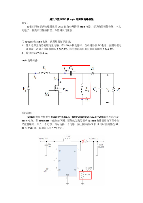
用升压型DCDC做sepic升降压电路经验摘要:有很多网友都试验过用升压DCDC做自动升降压sepic电路,都以烧毁器件告终,本文阐述了一种烧毁器件的机理,希望网友门注意。
用TD8208做sepic电路,试图达到如下需求:1.输入是带充电器的锂电池电路,有USB外接电源时,自动用外接5V电源,否则用锂电池电源,故输入电压范围为2.6V-5.2V,其中锂电池供电时电压范围是2.6V-4.2V。
2.输出为3.3V或4.1V。
sepic电路拓扑:实际电路:TD8208(兼容替代型号CE8303/FP6291/MT3608/STI3508/SY7152/SY7208)的典型应用是boost电路,从datasheet中截取如下图,要修改为满足需求的sepic电路需要将下图中红叉位置断开,串入一个电容,再对地接一个电感,如上图中的C1和L2.同时需要修改R2。
R2为150K时,输出电压为3.5V左右。
试验结果:当输入电压从2.6V开始上升,步进0.1V,在低于4V时,输出电压一直维持在3.5V,非常稳定,但当电压上升到4V以上时,输入电流立即剧增,若输入无限流装置芯片立即损坏。
结论是电路末达到设计要求。
原因分析:对比测试TD8208在标准boot模式下LX端子的波形,发现波形尖峰顶部始终没有超过8V,而在sepic模式下,在输入电压末达到4V左右时就几乎达到8V,且顶部平坦,当电压继续升高时,会继续升高,随即产生很大的输入电流,估计是内部保护动作了。
标准boot模式下LX端子的波形查阅datashee发现:TD8208的LX端子电压最大为7V,估计厂家是在内部做了保护,估计是这个保护电压对电路产生了影响。
分析sepic电路结构,发现LX端子电压要比标准boost电路时高。
内部MOS管导通时内部MOS管断开时可以看到,内部MOS管断开时,LX电压是L1上的电压+L2上的电压,而L2的电压是C1在MOS管导通时充的,故LX端电压基本上是2Vo。
HX3033 5V升21V升压芯片
w w w .h x s e m i .c o mF e a t u r e s2.2V Start-up Input Voltage Output Voltage as High as 28V 21V at 700mA from 5V Input Up to 88% EfficiencyProviding Flexibility for Using Internal andExternal Power Switches Small SOT23-6L PackageA p p l i c a t i o n sPDA DSC LCD Panel RF-Tags MP3Portable Instrument Wireless EquipmentD e s c r i p t i o nThe C is a compact, high efficiency, and low voltage step-up DC/DC converter with an Adaptive Current Mode PWM control loop, includes an error amplifier, ramp generator, comparator, switch pass element and driver in which providing a stable and high efficient operation over a wide range of load currents. It operates in stable waveforms without external compensation.HX3033 can operate from an input voltage as low as 2.2V. HX3033 can generate 21V up to 700mA from a 5V supply.The HX3033 is available in a low profile SOT-23-6L package.13509685286尚亿微电子李华T y p ic alA p p l i ca t i o n C i r c u i t* V OUT = 1.212V • [1 + (R1/R2)]P i n A s s i g n m e n t a n d F u n c t i o nAnalog Ground.2 SW Switch Pin. Connect inductor between SW and V Keep these PCB trace lengths as short and wide aspossible to reduce EMI and voltage overshoot. drive is derived from the greater of V Logic Controlled Shutdown Input. EN=High: Normal free running operation. EN=Low:Shutdown, quiescent current<1µA. 5 FBFeedback Input to the g Error Amplifier. Connectresistor divider tap to this pin. 6 PGNDPower Ground.A b s o l u t e M a x i m u m R a t i n g s (N o t e 1)Supply Voltage……………………………………………………………………….... −0.3V to 6.5V SW Pin Switch Voltage…………………………………………………………………−0.3V to 6.5V Other I/O Pin Voltages……………………………………………………….. −0.3V to (VDD + 0.3V) SW Pin Switch Current ………………………………………………………………...……………..1A Package Thermal Resistance (SOT-23-6)………………………………………………280 °C/W Operating Junction Temperature…………………………………………………….…………..125°C Storage Temperature Range ……………………………………………………….−65°C ~ +150°CN o t e 1: Absolute Maximum ratings are threshold limit values that must not be exceeded even for an instant under any conditions. Moreover, such values for any two items must not be reached simultaneously. Operation above these absolute maximum ratings may cause degradation or permanent damage to the device. These are stress ratings only and do not necessarily imply functional operation below these limits.E l e c t r i c a l C h a r a c t e r i s t i c s℃V IN=5V, V OUT set to 21V, unless otherwise specified.Operating Conditions: T A=25,Parameter Test Conditions MIN TYP MAX UNITS Start-UP Voltage I OUT = 1mA 2.2 V Operating VDD Range VDD Pin Voltage 2.5 5 V Supply Current (Quiescent) V FB = 1.2V 1300 μA Supply Current (Shutdown) EN = 0V 160 μA Feedback Reference Voltage 1.187 1.212 1.236 V Switching Frequency I OUT = 500mA 780 KHz Maximum Duty 100 % SW ON Resistance 0.3 ΩEN High Threshold V EN Rising 0.8 V EN Low Threshold 0.6 V EN Input Bias Current V EN = 0V, 5V 55 μANote: The EN pin shall be tied to VDD pin and inhibit to act the ON/OFF state whenever the VDD pin voltage may reach to 5.5V or above.T y p i c a l P e r f o r m a n c e C h a r a c t e r i s t i c sOperating Conditions: T A =25℃, unless otherwise specified.0.8Load Current(A)Load Current(A)Load Current(A)0.6Load Current(A)Output Voltage vs Load Current(Vout=10V)V OUT RippleV IN =5V, I LOAD =0.5A, V OUT =21VSW 10V/divM 1usB l o c k D i a g r a mA p p l i c a t i o n I n f o r m a t i o nInductor SelectionFor most applications, the value of the inductor will fall in the range of 1μH to 4.7μH. Its value is chosen based on the desired ripple current. Large value inductors lower ripple current and small value inductors result in higher ripple currents. Higher V IN or V OUT also increases the ripple current as shown in equation .A reasonable starting point for setting ripple current is △I L = 0.72A (40% of 1.8A).The DC current rating of the inductor should be at least equal to the maximum load current plus half the ripple current to prevent core saturation. Thus, a 2.16A rated inductor should be enough for most applications (1.8A + 0.36A). For better efficiency, choose a low DC-resistance inductor.Different core materials and shapes will change the size/current and price/current relationship of an inductor. Toroid or shielded pot cores in ferrite or perm alloy materials are small and don’t radiate much energy, but generally cost more than powdered iron core inductors with similar electrical characteristics. The choice of which style inductor to use often depends more on the price vs. size requirements and any radiated field/EMI requirements than on what VOUT5 requires to operate.Output and Input Capacitor SelectionIn continuous mode, the source current of the top MOSFET is a square wave of duty cycle V OUT/V IN. To prevent large voltage transients, a low ESR input capacitor sized for the maximum RMS current must be used. The maximum RMS capacitor current is given by:This formula has a maximum at V IN = 2V OUT, where I RMS = I OUT/2. This simple worst-case condition is commonly used for design because even significant deviations do not offer much relief. Note that the capacitor manufacturer’s ripple current ratings are often based on 2000 hours of life. This makes it advisable to further derate the capacitor, or choose a capacitor rated at a higher temperature than required. Always consult the manufacturer if there is any question.The selection of C OUT is driven by the required effective series resistance (ESR).Typically, once the ESR requirement for C OUT has been met, the RMS current rating generally far exceeds the I RIPPLE(P-P) requirement. The output ripple ΔV OUT is determined by:Where f = operating frequency, C OUT = output capacitance and ΔI L = ripple current in the inductor. For a fixed output voltage, the output ripple is highest at maximum input voltage since ΔI L increases with input voltage.Aluminum electrolytic and dry tantalum capacitors are both available in surface mount configurations. In the case of tantalum, it is critical that the capacitors are surge tested for use in switching power supplies. An excellent choice is the AVX TPS series of surface mount tantalum. These are specially constructed and tested for low ESR.Efficiency ConsiderationsThe efficiency of a switching regulator is equal to the output power divided by the input power times 100%. It is often useful to analyze individual losses to determine what is limiting the efficiency and which change would produce the most improvement. Efficiency can be expressed as: Efficiency = 100% - (L1+ L2+ L3+ ...) where L1, L2, etc. are the individual losses as a percentage of input power. Although all dissipative elements in the circuit produce losses, two main sources usually account for most of the losses: VIN quiescent current and I2R losses. The VIN quiescent current loss dominates the efficiency loss at very low load currents whereas the I2R loss dominates the efficiency loss at medium to high load currents. In a typical efficiency plot, the efficiency curve at very low load currents can be misleading since the actual power lost is of no consequence.1. The VIN quiescent current is due to two components: the DC bias current as given in the electrical characteristics and the internal main switch and synchronous switch gate charge currents. The gate charge current results from switching the gate capacitance of the internal power MOSFET switches. Each time the gate is switched from high to low to high again, a packet of charge △Q moves from VIN to ground. The resulting△Q/△t is the current out of VIN that is typically larger than the DC bias current. In continuous mode, I GATECHG = f (Q T+Q B) where Q T and Q B are the gate charges of the internal top and bottom switches. Both the DC bias and gate charge losses are proportional to VIN and thus their effects will be more pronounced at higher supply voltages.2. I2R losses are calculated from the resistances of the internal switches, R SW and external inductorR L. In continuous mode the average output current flowing through inductor L is “chopped” between the main switch and the synchronous switch. Thus, the series resistance looking into the SW pin is a function of both top and bottom MOSFET R DS(ON) and the duty cycle (DC) as follows: R SW =R DS(ON)TOP x DC + R DS(ON)BOT x (1-DC) The R DS(ON) for both the top and bottom MOSFETs can be obtained from the Typical Performance Characteristics curves. Thus, to obtain I2R losses, simply addR SW to R L and multiply the result by the square of the average output current. Other losses including CIN and COUT ESR dissipative losses and inductor core losses generally account for less than 2%of the total loss.Board Layout SuggestionsWhen laying out the printed circuit board, the following checklist should be used to ensure proper operation of the HX3033. Check the following in your layout:1. The power traces, consisting of the GND trace, the SW trace and the VIN trace should be keptshort, direct and wide.2. Put the input capacitor as close as possible to the device pins (VIN and GND).3. SW node is with high frequency voltage swing and should be kept small area. Keep analogcomponents away from SW node to prevent stray capacitive noise pick-up.4. Connect all analog grounds to a command node and then connect the command node to the powerground behind the output capacitors.P a c k a g i n g I n f o r m a t i o nSOT-23-6L Package Outline DimensionSymbolDimensions In Millimeters Dimensions In Inches MinMaxMinMaxA 1.050 1.250 0.041 0.049 A1 0.000 0.100 0.000 0.004 A2 1.0501.150 0.041 0.045b 0.300 0.500 0.012 0.020c 0.100 0.200 0.004 0.008 D 2.820 3.020 0.111 0.119 E 1.500 1.700 0.059 0.067 E1 2.6502.950 0.104 0.116e 0.950(BSC)0.037(BSC)e1 1.800 2.000 0.071 0.079 L 0.300 0.600 0.012 0.024 θ 0°8° 0° 8°。
hx711芯片资料

HX711称重传感器专用模拟/数字(A/D)转换器芯片简介HX711 是一款专为高精度称重传感器而设计的24位A/D 转换器芯片。
与同类型其它芯片相比,该芯片集成了包括稳压电源、片内时钟振荡器等其它同类型芯片所需要的外围电路,具有集成度高、响应速度快、抗干扰性强等优点。
降低了电子秤的整机成本,提高了整机的性能和可靠性。
该芯片与后端MCU 芯片的接口和编程非常简单,所有控制信号由管脚驱动,无需对芯片内部的寄存器编程。
输入选择开关可任意选取通道A 或通道B,与其内部的低噪声可编程放大器相连。
通道A 的可编程增益为128 或64,对应的满额度差分输入信号幅值分别为±20mV 或±40mV 。
通道B 则为固定的64 增益,用于系统参数检测。
芯片内提供的稳压电源可以直接向外部传感器和芯片内的A/D 转换器提供电源,系统板上无需另外的模拟电源。
芯片内的时钟振荡器不需要任何外接器件。
上电自动复位功能简化了开机的初始化过程。
特点两路可选择差分输入片内低噪声可编程放大器,可选增益为64 和128片内稳压电路可直接向外部传感器和芯片内A/D 转换器提供电源片内时钟振荡器无需任何外接器件,必要时也可使用外接晶振或时钟上电自动复位电路简单的数字控制和串口通讯:所有控制由管脚输入,芯片内寄存器无需编程可选择10Hz 或80Hz 的输出数据速率同步抑制50Hz 和60Hz 的电源干扰耗电量(含稳压电源电路):典型工作电流:< 1.7mA, 断电电流:< 1μA工作电压范围:2.6 ~ 5.5V工作温度范围:-20 ~ +85℃16 管脚的SOP-16 封装管脚说明。
dcdc升压芯片
dcdc升压芯片DC-DC升压芯片是一种能够将直流电压升高的集成电路,其原理是利用电感和电容的存储和释放能量来达到电压升高的目的。
在现代电子产品中,DC-DC升压芯片广泛应用于电池供电系统、光伏发电系统、无线通信系统等领域。
DC-DC升压芯片最早是用于电池供电系统,因为电池输出的电压通常较低,无法满足一些电子设备的工作需要。
通过使用DC-DC升压芯片,可以将电池输出的低压升高到设备所需的工作电压,从而保证设备的正常工作。
例如,现在智能手机的电池输出电压一般为3.7V左右,而手机芯片需要的工作电压通常在1.2V左右,因此需要使用DC-DC升压芯片将电池输出的3.7V电压升高到1.2V,供给芯片使用。
另外,DC-DC升压芯片还被广泛应用于光伏发电系统中。
在光伏发电系统中,太阳能电池板通过将光能转化为电能,输出直流电压。
然而,由于天气等因素的影响,太阳能电池板输出的电压通常较低,无法满足光伏发电系统的工作需要。
因此,需要使用DC-DC升压芯片将太阳能电池板输出的低压电压升高到适合发电系统工作的电压。
此外,DC-DC升压芯片还被广泛应用于无线通信系统中。
在无线通信系统中,无线模块通常需要较高的工作电压来实现远距离的信号传输。
然而,如何实现长距离的信号传输通常面临着电压降低的问题。
通过使用DC-DC升压芯片,可以将无线通信模块所需的工作电压从低压升高到适合信号传输的电压,有效解决了信号传输距离有限的问题。
目前市场上的DC-DC升压芯片种类繁多,常见的有开关电源芯片和线性电源芯片两种。
开关电源芯片通过开关管的控制来实现对电压的转换,具有转换效率高、体积小等优点,适用于功率较大的场合。
而线性电源芯片则通过控制电阻和电流的关系来实现对电压的升高,适用于功率较小、对效率要求不高的场合。
总之,在现代电子产品中,DC-DC升压芯片具有重要的应用价值,并在多个领域发挥着重要的作用。
随着电子设备的不断发展和工作电压的不断提高,DC-DC升压芯片的研究和应用将更加广泛,为电子产品的发展提供更多可能性和机遇。
YS3141E中文技术资料

11、联系方式: 天津越尔兴电子科技有限公司 地址:天津市海河工业园区聚兴道 9 号 电话:022-58653038 网址:
邮编:300350 传真:022-88919721-806
1)安装时要尽量减小施加到电路外壳或引线上的机械应力。 2)焊接温度要低于 260℃,时间小于 3 秒。 3)电路为 OC 输出,需要在 1、3 腿(电源与输出)之间加一上拉电阻。上拉电阻的阻值与工作
电压、通过电路的电流有关。 4)因为霍尔是敏感器件,请在仓储及生产过程中注意静电防护措施。 5)我们不建议您超越数据表中的参数使用,虽然在极限参数下霍尔会正常工作,但是长时间处
越尔兴技术咨询 QQ: 2719493142 电话 022-58653038
YS3141E 单极霍尔元件
中文数据手册
1、概述:
YS3141E 霍尔开关集成电路应用霍尔效应原理,采用半导体集成技术制造的磁敏电路,它是由 电压调整器、霍尔电压发生器、差分放大器、史密特触发器,温度补偿电路和集电极开路的输出级 组成的磁敏传感电路,其输入为磁感应强度,输出是一个数字电压讯号。具有较宽的工作电压范围 和较宽的工作温度范围,非常适合在汽车、工业电器和家电等产品中用作固态电子开关。 2、产品特点:
天津越尔兴电子科技有限公司 第 4 页 业务咨询 022-58653038
量值 单位
最小 典型 最大
4.5
-
24
V
- 0.2 0.4 V
- 0.1 10 μA
-
5
- mA
- 0.பைடு நூலகம் 2.0 μS
Altera发布第10代FPGA的30-Amp集成数字DC-DC转换器
Altera发布第10代FPGA的30-Amp集成数字DC-DC转换器Altera公司(NASDAQ: ALTR)在其越来越多的FPGA Enpirion电源解决方案中增加了30-amp PowerSoC DC-DC降压转换器。
30-amp EM1130是集成数字DC-DC降压转换器系列的第一款产品,为Altera的第10代FPGA提供电源管理功能,特别是Arria® 10和Stratix® 10 FPGA内核以及收发器电源轨。
自Altera于2013年成功收购Enpirion公司电源IC之后,EM1130数字电源管理器件是Altera努力为可编程逻辑市场提供最优电源解决方案的一个里程碑。
请通过/enpirion,详细了解EM1130和Altera的全系列电源解决方案,或者于3月15至19号北卡罗来纳州夏洛特举行的应用电源电子大会(APEC)上访问Altera展位,观看演示。
Altera业务部资深副总裁兼总经理Jeff Waters说:“通过这一创新,我们将为高端系列产品提供集成电源管理。
我们非常高兴看到过去18月中收购了Enpirion后的不断发展,电源和业界领先的FPGA平台紧密结合,希望客户能够继续从中受益。
”Altera DC/DC转换器简介Altera的DC/DC转换器实现了高密度、高性能、使用方便的电源解决方案。
为帮助节省电路板空间,同时满足严格的功率预算,Altera DC/DC转换器提供了简洁的负载点解决方案。
Altera DC/DC转换器提供增强小型封装,具有较高的开关频率,其集成电感减小了解决方案的大小。
低接通电阻集成MOSFET、严格的输出电压调节精度,以及先进的特性,这些使得Altera DC/DC转换器能够为业界最先进的FPGA供电。
EM1130 DC-DC转换器简介EM1130的引脚布局密度是业界最高的,提供严格的高输出稳压和快速瞬时响应功能。
这些特性支持基于FPGA的系统满足最严格的性能、功耗预算和解决方案大小要求。
LED升压、升降压的驱动恒流IC推荐二

LED升压、升降压的驱动恒流IC推荐宝剑锋从磨砺出,梅花香自苦寒来;此句是中国流传下来的一句古训,喻为如果想要取得成绩,获取成就,就要能吃苦,勤于锻炼,这样才能靠自己的努力赢得胜利。
各个行业皆是如此。
在电源网论坛里,就存在这样一些人,他们时常能DIY出被网友们称之为的经典设计,出于大家能够共同学习的目的,小编抓住了难得的机会,整理了这些经典帖,供分享学习。
本文续接上一篇LED升压、升降压的驱动恒流IC推荐一。
--------小编语。
美国美信集成产品公司MAX16831 可配置升降压型高功率LED驱动ICMAX16831是一款电流型、高亮LED (HBLED)驱动器,设计为通过控制2个外部n沟道MOSFET来调节单串LED的电流。
MAX16831集成了宽范围亮度控制、固定频率HBLED驱动器所需的全部组件。
MAX16831可配置为降压型(buck)、升压型(boost)或升/降压型(buck-boost)电流调节器。
带有前沿消隐的电流模式简化了控制回路的设计。
内部斜率补偿可在占空比超过50%时保持电流环路的稳定。
MAX16831工作于较宽的输入电压范围,并可承受汽车抛负载事件。
多个MAX16831可相互同步或同步至外部时钟。
MAX16831包含一个浮动亮度驱动器,驱动串联在LED串的n沟道MOSFET实现亮度控制。
使用MAX16831架构的HBLED驱动器可在汽车应用中实现超过90%的效率。
MAX16831还包括一个可源出1.4A、吸收2.5A电流(sink)的栅极驱动器,用于在高功率LED驱动器应用中驱动开关MOSFET,如车灯总成等。
亮度控制允许宽范围的PWM调光,其频率可高达2kHz。
在较低的调光频率下可实现高达1000:1的调光比。
MAX16831提供带裸焊盘的32引脚薄型QFN封装,工作于-40°C至+125°C汽车级温基本参数:宽输入范围:6V至76V;集成LED电流检测差分放大器;可驱动n沟道MOSFET;具有浮动亮度驱动能力;LED电流精度:5%;200Hz片上斜坡发生器,可同步至外部PWM亮度信号;可编程开关频率(125kHz至600kHz),可被同步;输出过压、负载开路、LED短路、过热保护;低至107mV LED电流检测可提高效率;使能/关断输入,关断电流低于45µA。
常见的电源管理IC,DC-DC升压芯片,DC-DC降压芯片,同步升压IC,降压横流IC,MOS管
常见的电源管理IC,DC-DC升压芯片,DC-DC降压芯片,同步升压IC,降压横流IC,MOS 管等DC-DC升压IC型号工作模式输出电压(V)启动电压(V)电压输出精度(%)转换效率输出流(mA)静态电流(uA)开关频率(KHz)封装形式可替代型号LYxxC PFM 2.7/3.0/3.3/5.0V 0.8V ±2.5% 86% 300mA 6 uA 100KHz SOT-23SOT89-3 TOREX: CX6383SEIKO: S832 RICOH: RH5RI RICHTEK: RT9261LY21Axx PFM 2.7/3.0/3.3/3.6/4.5/5.0/5.6 0.8 V ±2.5% 90% 400 6 100 SOT-23SOT89-3 TOREX: CX6383SEIKO: S832 RICOH: RH5RI RICHTEK: RT9261LY21Bxx PFM 3.3/5.0/5.6 0.8 ±2.5% 90% <400 6 100 SOT23SOT89-3 TOREX: CX6383 SEIKO: S832 RICOH: RH5RIRICHTEK: RT9261LY21Cxx PFM 3.0/3.3/3.6/4.5/5.0/5.6 0.8 ±2.5% 90% 400 6 100 SOT23-5 TOREX: CX6383 SEIKO: S832 RICOH: RH5RIRICHTEK: RT9261LY21Dxx PFM 3.0/3.3/3.6/4.5/5.0/5.6 0.8 ±2.5% 90% <400 6 100 SOT23-5 TOREX: CX6383 SEIKO: S832RICOH: RH5RI RICHTEK: RT9261LY21F PFM ADJ 0.8 ±2.5% 90% <400 6 100 SOT23-5 TOREX: CX6383 SEIKO:S832 RICOH: RH5RI RICHTEK: RT9261LY21(PWM) PWM 3.0/3.3/3.6/4.5/5.0/5.6 0.8 ±2.5% 90% 400 6 100 SOT23 SOT89-3 TOREX: CX6383 SEIKO: S832RICOH: RH5RI RICHTEK: RT9261LY2100系列PFM 2.7/3.0/3.3/3.6/4.5/5.0/5.6 0.8 ±2.5% 90% 400 6 100 SOT23 SOT89-3 TOREX: CX6383 SEIKO: S832 RICOH: RH5RI RICHTEK: RT9261LY2101系列PWM 2.7/3.0/3.3/3.6/4.5/5.0/5.6 0.8 ±2.5% 90% 400 6 100 SOT23 SOT89-3 TOREX: CX6383 SEIKO: S832 RICOH: RH5RI RICHTEK: RT9261LY2108系列PFM 2.7/3.0/3.3/3.6/4.5/5.0/5.6 0.8 ±2.5% 90% 400 6 100 SOT23 SOT89-3 TOREX: CX6383 SEIKO: S832 RICOH: RH5RI RICHTEK: RT9261LY3400 PWM ADJ 0.6 ±2.5% 97% 400 6 100 SOT23-6 LTC34002.DC-DC降压IC型号工作模式输出电压(V)输入电压(V)电压输出精度(%)转换效率输出电流(mA)静态电流(uA)开关频率(KHz)封装形式可替代型号LY3406A PWM 1.2/1.8/3.3/ADJ 0.9-6.5 ±2.0% 97% 600 1 1.5M SOT23-5 LTC3406LY3406B PFM/PWM 1.2/1.8/3.3/ADJ 0.9-6.5 ±2.0% 97% 600 1 1.5M SOT23-5 XC9216LY34063 PWM ADJ 3-40 ±2.0% 89% 1.2A/1.5A 23 52 SOP8LM34063,ST34063,MC340633.DC-DC反转倍压芯片型号工作模式输出电压(V)输入电压(V)电压输出精度(%)转换效率输出电流(mA)静态电流(uA)开关频率(KHz)封装形式可替代型号LY7660 DC/DC 电荷泵电压反转IC 1.5-10 99.90% 98% 40 10 SOP8,DIP8 ICL7660LY7661 三倍压DC/DC 电荷电压反转IC 1.5-6 99.90% 98% 2 20 SOP14,DIP14 SCI76614.LDO线性稳压IC型号工作模式输出电压(V)最高输入(V)电压输出精度(%)输出电流(mA)静态电流(uA)封装形式可替代型号LY6206A CMOS线性稳压器1.2/1.5/1.8/2.0/2.1/2.5/2.7/2.8/3.0/3.3/3.5/3.6 6.5 2% 300 3 SOT23,SOT89 TOREX:XC6206LY6206C 1.2/1.3/1.5/1.8/2.5/2.7/2.8/3.0/3.3 6.5 2% 300 65 SOT23-5RICHTEK:RT9193,TOREX:XC6219LY6206K 3.3 6.5 2% 300 5 SOT89-3TOREX:XC6206LY6206K1 3.3 6.5 2% 300 5 SOT89-3 TOREX:XC6206LY6206L 3.3 6.5 2% <400 8 SOT89-3TOREX:XC6206LY6211A 3.3 6.5 2% 500 50 SOT89-3 TOREX:XC6206LY6219 1.2---3.6 6.5 2% 300 65 SOT23,SOT89 RICHTEK:RT9193,TOREX:XC6219LY1117 1.2/1.5/1.8/2.5/3.3/5/ADJ 6.5 2% 300 2mA SOT89,SOT223 LM1117LY6204 1.2---3.6 6.5 2% 300 3 SOT89,SOT23TOREX:XC6204LY6401 2.8&1.8/1.8&2.8/1.8&2.5/3.3&3.3 6.5 2% 300 130 SOT23-5,SOT23-6TOREX:XC6401LY6411 1.5&3.0 6.5 2% 300 16 SOT23-5,SOT23-6 TOREX:XC64115.耐高压LDO型号工作模式输出电压(V)最高输入(V)电压输出精度(%)输出电流(mA)静态电流(uA)封装形式可替代型号LY71xx CMOS线性稳压器3.0/3.3/3.6/4.4/5.0 24 3% 50 3SOT89,TO92 HOLTEK:HT71xxLY75xx 3.0/3.3/3.6/4.4/5.0 24 3% 100 3 SOT89,TO92HOLTEK:HT75xxLY73xx 3.0/3.3/3.6/4.4/5.0 24 3% 300 3 SOT89,TO92HOLTEK:HT73xxLY6201Axx 3.0/3.3/3.6/4.4/5.0 24 2% 120 3 SOT89,TO92HOLTEK:HT75xx6.低电压检测IC&复位IC型号工作模式输出电压(V)输入电压(V)电压输出精度(%)复位时间(ms)静态电流(mA)封装形式可替代型号LY61Cxx C-沟道2.1/2.2/2.5/2.7/3.3/4.0/4.3/4.1 0.7-10 1% 10 SOT23,SOT89 TOREX:XC61CCLY61Nxx N-沟道 1.8/2.2/2.5/2.7/3.0/3.3/3.5/3.8/4.2/4.3 0.7-10 1% 10 SOT23,SOT89 TOREX:XC61CNLY809 C-沟道2.63/2.7/2.93/3.08 0.3-6 1% 140 10 SOT23,SOT89MAX809LY810 N-沟道2.63/2.7/2.93/3.08 0.3-6 1% 140 10 SOT23,SOT89MAX810LY2801A C-沟道1.1-6 0.7-10 1% 10 SOT23,SOT89 TOREX:XC61CCLY2802A N-沟道1.1-6 0.7-10 1% 10 SOT23,SOT89 TOREX:XC61CN7.充电保护管理IC型号工作特征输入电压(V)电压输出精度(%)/最大充电电流(mA)静态电流(uA)封装形式可替代型号LY4054充电电流监测,输入低电压闭锁4.25-6.5 1% 800 25 SOT23-5LY4056充电电流监测,输入低电压闭锁4.25-6.5 1% 1A 25 SOP8LY-DW01锂电池保护IC 1% SOT23-6,SOP8LY8205 MOSFET 1% SOT23-6,SOP88.LED恒流驱动IC型号工作特征最佳输出电流输入电压(V)输出电压(V)输出精度(%)转换效率静态电流(uA)封装形式可替代型号LY2106F升压恒流500Ma 0.9-6.5 5% 86% 20 SOT89-5 BL8532LY2206 升压恒流1A 0.8-3 5 86% 1 SOT23-6 PAM2803LY2305升压恒流1.5A 2.5-12 2.8-40 5 86% SOP8 ZXLD300LY7135系列降压恒流220mA/260mA/280mA/300mA/320mA/350mA/ 2.7-6 5 90%SOT89-3 AMC7135,T6335ALY7136降压恒流<350,可调2.7-6 5 90% SOT89-3LY5241降压恒流可调5.5-40 5 85% SOT23-6 ZXLD1350,ZXLD1360,PT4115,PAM2863LY9910降压恒流可调AC85-265 5 87% SOP8 HV9910LY9920降压恒流可调3.6-60 5 86% SOT23-6 PT41059.N-MOS管/P-MOS管型号工作特征最大漏源电压(V)最大栅源电压(V)最大电流(A)Rds(on)封装形式可替代型号LY2302 N-MOS 20V 8V 3A 29mΩSOT23 SI2302LY2306 N-MOS 20V 10V 5A 23mΩSOP8 CEM9926LY2308 N-MOS 20V 12V 6A 21mΩTSSOP8 CEG8205LY2310 N-MOS 30V 12V 5.7A 32mΩSOT23 AO3400LY2316 N-MOS 20V 12V 6A 22mΩSOT23-6 CEG8205LY2318 N-MOS 20V 12V 6A 19mΩTSSOP8 SI6968BEDQLY2301 P-MOS -20V -8V -3.1A 100mΩSOT23 SI2301LY2303 P-MOS -30V -12V -4.3A 50mΩSOT23 AO3401LY2307 P-MOS -30V -20V -4.3A 78mΩSOT23 AO3407,AO3409LY2309 P-MOS -30V -20V -6A 53mΩSOP8 FDS9435LY2311 P-MOS -30V -20V -6A 53mΩSOP8 FDS4953。
高效率反激开关电源的设计
江苏科技大学本科毕业设计(论文)学院电气与信息工程学院专业电子信息工程学生姓名李和琦班级学号0945531122指导教师丁伟二零一三年六月江苏科技大学本科毕业论文18W高效率反激开关电源的设计Design of 18W Efficient Flyback Switching Power Supply摘要任何电子设备都离不开可靠的电源,而对于采用电网电源的家用电子设备,其直流电源必须具有适应电网电压变化和负载变化的特性。
为此而发展的的直流稳压电源成为电子设备电路中的一个非常重要的组成部分。
开关电源是利用现代电力电子技术,以高频变压器代替工频变压器,采用脉宽调制技术的交流-直流的稳压电源,它具有管耗小,效率高,稳压范围宽及体积小,重量轻等特点,并广泛应用于工业自动化控制,军工设备,科研设备,LED照明,工控设备,通讯设备,电力设备,仪器设备,医疗设备,半导体制冷等领域。
本文主要内容如下:1.了解开关电源的基本结构,阅读开关电源相关文献,确定毕业设计所要做的内容;2.对开关电源的基本工作原理进行分析,对电源的buck工作模式,boost工作模式,buck-boost工作模式以及flybuck工作模式进行分析比较,最终选择适用于反激开关电源的flybuck工作模式;3.查阅资料学习了设计开关电源的基本方法,以及在设计过程中所需要掌握的原理,设计出一款输出功率为18W,输出电压与电流分别为12V,1.5A,文波小于150mV的高效率反激式开关电源;4.对设计出的实物进行波形分析。
测试其在工作过程中buck电容的电压电流变化,RCD回路上的电压吸收情况,MOS管在高压和断续时的Vds和Vgs电压,空载时的Vcc和Vds电压以及Sense电阻上的电压,对实物的基本特性进行测试。
关键词:直流稳压电源,开关电源,脉宽调制,反激式,高效率AbstractAny electronic devi ce can’t do without reliable power, As for the use of grid power home electronics equipment, The DC power supply must have to adapt to changes in grid voltage and load characteristics. To this end the development of the DC power supply circuit in electronic devices become a very important part.Switching power supply is the use of modern power electronics,High frequency transformers instead of frequency transformers, Using pulse width modulation DC - DC power supply,It has consumed a small tube, high efficiency, wide voltage range and small size, light weight, And is widely used in industrial automation, military equipment, scientific equipment, LED lighting, industrial control equipment, communications equipment, electrical equipment, apparatus equipment, medical equipment, semiconductor refrigeration and other fields.The graduation design process, mainly for the following:1. Understand the basic structure of the switch power supply, switch power supply related literature, to determine the content of the graduation design to do;2. Analyze the basic working principle of switch power supply, the power of the buck mode, boost the work mode, buck - boost work models and flybuck work carries on the analysis comparison, the final choice is suitable for the flyback switching power supply of flybuck working mode;3. To learn the basic methods of design of switch power supply, and the need to master the principle in the design process, and designed A power output of 18 w, output voltage and current respectively for 12 V, 1.5 A, less than 150 mV Wen Bo the flyback type switch power supply with high efficiency;4. The waveform analysis was carried out on the design of physical objects. Test the buck in the working process of the capacitor voltage current changes, RCD circuit voltage absorption.Keywords:Dc regulated power supply, Switching power supply, Pulse width modulation, the flyback type, High efficiency目录第一章绪论 (1)1.1 研究背景与发展状况 (1)1.2 开关电源相关介绍 (2)1.3 本章小结 (3)第二章开关电源的工作原理介绍 (4)2.1 基本拓扑结构 (4)2.1.1 Buck降压变换器 (4)2.1.2 Boost升压变换器 (6)2.1.3 Buck-Boost降压或升压变换器 (7)2.2 Flyback模式 (9)2.2.1 Buck-Boost拓扑Flyback (9)2.2.2 工作原理 (9)2.2.3 主要关系推导 (12)2.3本章小结 (13)第三章开关电源基本结构及元器件介绍 (14)3.1 开关电源基本结构 (14)3.2 开关电源主要器件 (15)3.2.1 TL431 (15)3.2.2 通嘉LD7531 (16)3.2.3 光耦 (16)3.2.4 安规电容 (17)3.3 本章小结 (17)第四章反激式开关电源的参数计算 (18)4.1课题介绍 (18)4.2 原理图和一般工作过程 (18)4.3 确定DC电压范围和输入整流滤波电容 (19)4.3.1 确定DC电压范围 (19)4.3.2 确定整流滤波电容 (20)4.4 反激式变压器的设计 (20)4.5 确定次级整流二极管 (24)4.6 确定输出电容 (24)4.7 RCD缓冲器的参数设计 (24)4.8 反馈回路的参数设计 (27)4.9 Sense电阻大小的确定 (28)4.10 安规电容的参数确定 (28)4.11提高效率的方法 (29)4.12 本章小结 (30)第五章反激式开关电源的产品测试 (31)5.1 基本测试 (31)5.2 波形分析 (31)5.3 本章小结 (36)结论 (37)致谢 (38)参考文献 (39)第一章绪论1.1 研究背景与发展状况电源按工作状态一般可分为线性电源,开关电源。
常用开关电源芯片大全

常用开关电源芯片大全第1章DC-DC电源转换器/基准电压源1.1 DC-DC电源转换器1.低噪声电荷泵DC-DC电源转换器AAT3113/AAT31142.低功耗开关型DC-DC电源转换器ADP30003.高效3A开关稳压器AP15014.高效率无电感DC-DC电源转换器FAN56605.小功率极性反转电源转换器ICL76606.高效率DC-DC电源转换控制器IRU30377.高性能降压式DC-DC电源转换器ISL64208.单片降压式开关稳压器L49609.大功率开关稳压器L4970A11.2A高效率单片开关稳压器L497812.1A高效率升压/降压式DC-DC电源转换器L597014.高效率1A降压单片开关稳压器LM1575/LM2575/LM2575HV15.3A降压单片开关稳压器LM2576/LM2576HV16.可调升压开关稳压器LM257717.3A降压开关稳压器LM259618.高效率5A开关稳压器LM267819.升压式DC-DC电源转换器LM2703/LM270420.电流模式升压式电源转换器LM273321.低噪声升压式电源转换器LM275022.小型75V降压式稳压器LM500723.低功耗升/降压式DC-DC电源转换器LT107324.升压式DC-DC电源转换器LT161525.隔离式开关稳压器LT172526.低功耗升压电荷泵LT175127.大电流高频降压式DC-DC电源转换器LT176528.大电流升压转换器LT193529.高效升压式电荷泵LT193730.高压输入降压式电源转换器LT195632.高压升/降压式电源转换器LT343333.单片3A升压式DC-DC电源转换器LT343634.通用升压式DC-DC电源转换器LT346035.高效率低功耗升压式电源转换器LT346437.大电流高效率升压式DC-DC电源转换器LT378238.微型低功耗电源转换器LTC175440.低噪声高效率降压式电荷泵LTC191141.低噪声电荷泵LTC3200/LTC3200-542.无电感的降压式DC-DC电源转换器LTC325143.双输出/低噪声/降压式电荷泵LTC325244.同步整流/升压式DC-DC电源转换器LTC340145.低功耗同步整流升压式DC-DC电源转换器LTC340246.同步整流降压式DC-DC电源转换器LTC340547.双路同步降压式DC-DC电源转换器LTC340748.高效率同步降压式DC-DC电源转换器LTC341649.微型2A升压式DC-DC电源转换器LTC342650.2A两相电流升压式DC-DC电源转换器LTC342851.单电感升/降压式DC-DC电源转换器LTC344052.大电流升/降压式DC-DC电源转换器LTC344254.直流同步降压式DC-DC电源转换器LTC370355.双输出降压式同步DC-DC电源转换控制器LTC373656.降压式同步DC-DC电源转换控制器LTC377057.双2相DC-DC电源同步控制器LTC380258.高性能升压式DC-DC电源转换器MAX1513/MAX151459.精简型升压式DC-DC电源转换器MAX1522/MAX1523/MAX152460.高效率40V升压式DC-DC电源转换器MAX1553/MAX155461.高效率升压式LED电压调节器MAX1561/MAX159962.高效率5路输出DC-DC电源转换器MAX156563.双输出升压式DC-DC电源转换器MAX1582/MAX1582Y64.驱动白光LED的升压式DC-DC电源转换器MAX158365.高效率升压式DC-DC电源转换器MAX1642/MAX164366.2A降压式开关稳压器MAX164467.高效率升压式DC-DC电源转换器MAX1674/MAX1675/MAX167668.高效率双输出DC-DC电源转换器MAX167769.低噪声1A降压式DC-DC电源转换器MAX1684/MAX168570.高效率升压式DC-DC电源转换器MAX169871.高效率双输出降压式DC-DC电源转换器MAX171572.小体积升压式DC-DC电源转换器MAX1722/MAX1723/MAX172473.输出电流为50mA的降压式电荷泵MAX173074.升/降压式电荷泵MAX175975.高效率多路输出DC-DC电源转换器MAX180076.3A同步整流降压式稳压型MAX1830/MAX183177.双输出开关式LCD电源控制器MAX187878.电流模式升压式DC-DC电源转换器MAX189679.具有复位功能的升压式DC-DC电源转换器MAX194780.高效率PWM降压式稳压器MAX1992/MAX199381.大电流输出升压式DC-DC电源转换器MAX61882.低功耗升压或降压式DC-DC电源转换器MAX62983.PWM升压式DC-DC电源转换器MAX668/MAX66984.大电流PWM降压式开关稳压器MAX724/MAX72685.高效率升压式DC-DC电源转换器MAX756/MAX75786.高效率大电流DC-DC电源转换器MAX761/MAX76287.隔离式DC-DC电源转换器MAX8515/MAX8515A88.高性能24V升压式DC-DC电源转换器MAX872789.升/降压式DC-DC电源转换器MC33063A/MC34063A90.5A升压/降压/反向DC-DC电源转换器MC33167/MC3416791.低噪声无电感电荷泵MCP1252/MCP125392.高频脉宽调制降压稳压器MIC220393.大功率DC-DC升压电源转换器MIC229594.单片微型高压开关稳压器NCP1030/NCP103195.低功耗升压式DC-DC电源转换器NCP1400A96.高压DC-DC电源转换器NCP140397.单片微功率高频升压式DC-DC电源转换器NCP141098.同步整流PFM步进式DC-DC电源转换器NCP142199.高效率大电流开关电压调整器NCP1442/NCP1443/NCP1444/NCP1445 100.新型双模式开关稳压器NCP1501101.高效率大电流输出DC-DC电源转换器NCP1550102.同步降压式DC-DC电源转换器NCP1570103.高效率升压式DC-DC电源转换器NCP5008/NCP5009104.大电流高速稳压器RT9173/RT9173A105.高效率升压式DC-DC电源转换器RT9262/RT9262A106.升压式DC-DC电源转换器SP6644/SP6645107.低功耗升压式DC-DC电源转换器SP6691108.新型高效率DC-DC电源转换器TPS54350109.无电感降压式电荷泵TPS6050x110.高效率升压式电源转换器TPS6101x111.28V恒流白色LED驱动器TPS61042112.具有LDO输出的升压式DC-DC电源转换器TPS6112x113.低噪声同步降压式DC-DC电源转换器TPS6200x114.三路高效率大功率DC-DC电源转换器TPS75003115.高效率DC-DC电源转换器UCC39421/UCC39422116.PWM控制升压式DC-DC电源转换器XC6371117.白光LED驱动专用DC-DC电源转换器XC9116118.500mA同步整流降压式DC-DC电源转换器XC9215/XC9216/XC9217 119.稳压输出电荷泵XC9801/XC9802120.高效率升压式电源转换器ZXLB16001.2 线性/低压差稳压器121.具有可关断功能的多端稳压器BAXXX122.高压线性稳压器HIP5600123.多路输出稳压器KA7630/KA7631124.三端低压差稳压器LM2937125.可调输出低压差稳压器LM2991126.三端可调稳压器LM117/LM317127.低压降CMOS500mA线性稳压器LP38691/LP38693 128.输入电压从12V到450V的可调线性稳压器LR8129.300mA非常低压降稳压器(VLDO)LTC3025130.大电流低压差线性稳压器LX8610131.200mA负输出低压差线性稳压器MAX1735132.150mA低压差线性稳压器MAX8875133.带开关控制的低压差稳压器MC33375134.带有线性调节器的稳压器MC33998136.低静态电流低压差稳压器NCP562/NCP563137.具有使能控制功能的多端稳压器PQxx138.五端可调稳压器SI-3025B/SI-3157B139.400mA低压差线性稳压器SPX2975140.五端线性稳压器STR20xx141.五端线性稳压器STR90xx142.具有复位信号输出的双路输出稳压器TDA8133143.具有复位信号输出的双路输出稳压器TDA8138/TDA8138A 144.带线性稳压器的升压式电源转换器TPS6110x145.低功耗50mA低压降线性稳压器TPS760xx146.高输入电压低压差线性稳压器XC6202147.高速低压差线性稳压器XC6204148.高速低压差线性稳压器XC6209F149.双路高速低压差线性稳压器XC64011.3 基准电压源150.新型XFET基准电压源ADR290/ADR291/ADR292/ADR293 151.低功耗低压差大输出电流基准电压源MAX610x152.低功耗1.2V基准电压源MAX6120155.低功耗精密低压降基准电压源REF30xx/REF31xx156.精密基准电压源TL431/KA431/TLV431A第2章AC-DC转换器及控制器1.厚膜开关电源控制器DP104C2.厚膜开关电源控制器DP308P3.DPA-Switch系列高电压功率转换控制器DPA423/DPA424/DPA425/DPA4264.电流型开关电源控制器FA13842/FA13843/FA13844/FA138455.开关电源控制器FA5310/FA53116.PWM开关电源控制器FAN75567.绿色环保的PWM开关电源控制器FAN76018.FPS型开关电源控制器FS6M07652R9.开关电源功率转换器FS6Sxx10.降压型单片AC-DC转换器HV-2405E11.新型反激准谐振变换控制器ICE1QS0112.PWM电源功率转换器KA1M088013.开关电源功率转换器KA2S0680/KA2S088014.电流型开关电源控制器KA38xx15.FPS型开关电源功率转换器KA5H0165R16.FPS型开关电源功率转换器KA5Qxx17.FPS型开关电源功率转换器KA5Sxx18.电流型高速PWM控制器L499019.具有待机功能的PWM初级控制器L599120.低功耗离线式开关电源控制器L659021.LINK SWITCH TN系列电源功率转换器LNK304/LNK305/LNK30622.LINK SWITCH系列电源功率转换器LNK500/LNK501/LNK52023.离线式开关电源控制器M51995A24.PWM电源控制器M62281P/M62281FP25.高频率电流模式PWM控制器MAX5021/MAX502226.新型PWM开关电源控制器MC4460427.电流模式开关电源控制器MC4460528.低功耗开关电源控制器MC4460829.具有PFC功能的PWM电源控制器ML482430.液晶显示器背光灯电源控制器ML487631.离线式电流模式控制器NCP120032.电流模式脉宽调制控制器NCP120533.准谐振式PWM控制器NCP120734.低成本离线式开关电源控制电路NCP121535.低待机能耗开关电源PWM控制器NCP123036.STR系列自动电压切换控制开关STR8xxxx37.大功率厚膜开关电源功率转换器STR-F665438.大功率厚膜开关电源功率转换器STR-G865639.开关电源功率转换器STR-M6511/STR-M652940.离线式开关电源功率转换器STR-S5703/STR-S5707/STR-S570841.离线式开关电源功率转换器STR-S6401/STR-S6401F/STR-S6411/STR-S6411F 442.开关电源功率转换器STR-S651343.离线式开关电源功率转换器TC33369~TC3337444.高性能PFC与PWM组合控制集成电路TDA16846/TDA1684745.新型开关电源控制器TDA1685046.“绿色”电源控制器TEA150447.第二代“绿色”电源控制器TEA150748.新型低功耗“绿色”电源控制器TEA153349.开关电源控制器TL494/KA7500/MB375950.Tiny SwitchⅠ系列功率转换器TNY253、TNY254、TNY25551.Tiny SwitchⅡ系列功率转换器TNY264P~TNY268G52.TOP Switch(Ⅱ)系列离线式功率转换器TOP209~TOP22753.TOP Switch-FX系列功率转换器TOP232/TOP233/TOP23454.TOP Switch-GX系列功率转换器TOP242~TOP25055.开关电源控制器UCX84X56.离线式开关电源功率转换器VIPer12AS/VIPer12ADIP57.新一代高度集成离线式开关电源功率转换器VIPer53第3章功率因数校正控制/节能灯电源控制器1.电子镇流器专用驱动电路BL83012.零电压开关功率因数控制器FAN48223.功率因数校正控制器FAN75274.高电压型EL背光驱动器HV8265.EL场致发光背光驱动器IMP525/IMP5606.高电压型EL背光驱动器/反相器IMP8037.电子镇流器自振荡半桥驱动器IR21568.单片荧光灯镇流器IR21579.调光电子镇流器自振荡半桥驱动器IR215910.卤素灯电子变压器智能控制电路IR216111.具有功率因数校正电路的镇流器电路IR216612.单片荧光灯镇流器IR216713.自适应电子镇流器控制器IR252014.电子镇流器专用控制器KA754115.功率因数校正控制器L656116.过渡模式功率因数校正控制器L656217.集成背景光控制器MAX8709/MAX8709A18.功率因数校正控制器MC33262/MC3426219.固定频率电流模式功率因数校正控制器NCP165320.EL场致发光灯高压驱动器SP440321.功率因数校正控制器TDA4862/TDA486322.有源功率因数校正控制器UC385423.高频自振荡节能灯驱动器电路VK05CFL24.大功率高频自振荡节能灯驱动器电路VK06TL第4章充电控制器1.多功能锂电池线性充电控制器AAT36802.可编程快速电池充电控制器BQ20003.可进行充电速率补偿的锂电池充电管理器BQ20574.锂电池充电管理电路BQ2400xB接口单节锂电池充电控制器BQ2402x7.2A同步开关模式锂电池充电控制器BQ241008.集成PWM开关控制器的快速充电管理器BQ29549.具有电池电量计量功能的充电控制器DS277010.锂电池充电控制器FAN7563/FAN756411.2A线性锂/锂聚合物电池充电控制器ISL629212.锂电池充电控制器LA5621M/LA5621V14.2A恒流/恒压电池充电控制器LT176915.线性锂电池充电控制器LTC173216.带热调节功能的1A线性锂电池充电控制器LTC173317.线性锂电池充电控制器LTC173418.新型开关电源充电控制器LTC198019.开关模式锂电池充电控制器LTC400220.4A锂电池充电器LTC400621.多用途恒压/恒流充电控制器LTC400823.可由USB端口供电的锂电池充电控制器LTC405324.小型150mA锂电池充电控制器LTC405425.线性锂电池充电控制器LTC405826.单节锂电池线性充电控制器LTC405927.独立线性锂电池充电控制器LTC406128.镍镉/镍氢电池充电控制器M62256FP29.大电流锂/镍镉/镍氢电池充电控制器MAX150130.锂电池线性充电控制器MAX150731.双输入单节锂电池充电控制器MAX1551/MAX155532.单节锂电池充电控制器MAX167933.小体积锂电池充电控制器MAX1736B接口单节锂电池充电控制器MAX181135.多节锂电池充电控制器MAX187336.双路输入锂电池充电控制器MAX187438.低成本/多种电池充电控制器MAX190839.开关模式单节锂电池充电控制器MAX1925/MAX192640.快速镍镉/镍氢充电控制器MAX2003A/MAX200341.可编程快速充电控制器MAX712/MAX71342.开关式锂电池充电控制器MAX74543.多功能低成本充电控制器MAX846A44.具有温度调节功能的单节锂电池充电控制器MAX8600/MAX860145.锂电池充电控制器MCP73826/MCP73827/MCP7382846.高精度恒压/恒流充电器控制器MCP73841/MCP73842/MCP73843/MCP73844 647.锂电池充电控制器MCP73861/MCP7386248.单节锂电池充电控制器MIC7905049.单节锂电池充电控制器NCP180050.高精度线性锂电池充电控制器VM7205。
ZS6300三合一同步升压移动电源芯片
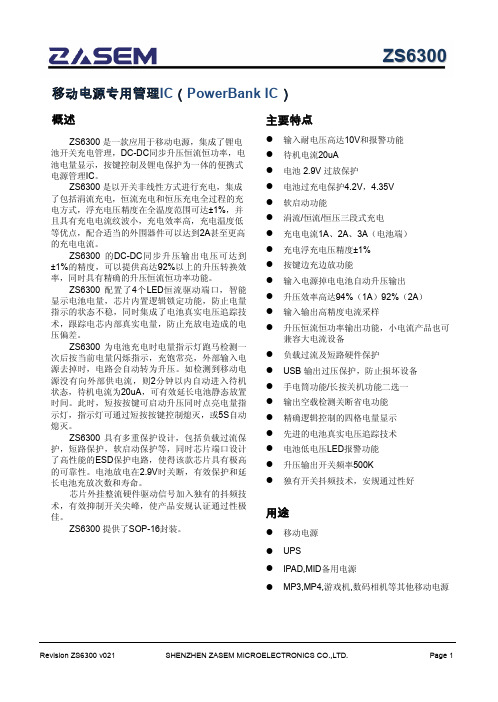
负载过流及短路硬件保护 USB 输出过压保护,防止损坏设备 手电筒功能/长按关机功能二选一 输出空载检测关断省电功能 精确逻辑控制的四格电量显示 先进的电池真实电压追踪技术 电池低电压LED报警功能 升压输出开关频率500K 独有开关抖频技术,安规通过性好
Revision ZS6300 v021
SHENZHEN ZASEM MICROELECTRONICS CO.,LTD.
Page 3
极限参数
参数 输入电压 输入电压 工作温度范围 工作结温范围 储存温度 引脚焊接温度(10 sec)
符号 VIN VSYS TOP TJ TST TLEAD
ZS6300
Page 4
ZS6300
符号
VIN-OVP
ITAP
VTAP
VBAT ICONST ITRKL IFULL
VTRKL
VRECHG
VCUR_BALANCE
FLED
TTAP TBSTDEL THOLD VNOLOADOFF TNOLOADOFF VBSTL VLOWQOFF TLOWQOFF VLOWQ_FLASH FLOWQ_FLASH TOFF_SLEEP V LOAD-LIMC VLOAD-OVC TOVC-OFF
流减小到恒流充电电流的 1/10 时,4 个 LED 灯全部常亮,指示电池已经充饱。充饱时,电池终止充电,等
待电池电压降低到一定电压(VRECHG)时进行复充(Recharge)。
2. 充电电流设定
对电池充电的电流大小由芯片的 SNS 引脚和 BAT 引脚之间的采样电阻 RS 来设定。恒流充电电流 ICharge
电池正极引脚,检测电池电压和充电电流采样引脚 高端电流采样引脚
- 1、下载文档前请自行甄别文档内容的完整性,平台不提供额外的编辑、内容补充、找答案等附加服务。
- 2、"仅部分预览"的文档,不可在线预览部分如存在完整性等问题,可反馈申请退款(可完整预览的文档不适用该条件!)。
- 3、如文档侵犯您的权益,请联系客服反馈,我们会尽快为您处理(人工客服工作时间:9:00-18:30)。
HX1001 T i n y P a c k a g e,H i g h E f f i c i e n c y,S t e p-u pF e a t u r e sInput Voltage Range: 1.1V~5.5V Internal MOSFET with high switch current up to 3A90% EfficiencyUp to 450kHz Switching Frequency SOT-23-6L PackageA p p l i c a t i o n sPDADSCLCD PanelRF-TagsMP3Portable InstrumentsWireless Equipments D e s c r i p t i o nThe HX3141 is a compact, high efficiency, and low voltage step-up DC/DC converter including an error amplifier, ramp generator, comparator, switch pass element and driver in which providing a stable and high efficient operation over a wide range of load currents. It operates in stable waveforms without external compensation.The high switching rate minimized the size of external components. Besides, the low quiescent current together with high efficiency maintains long battery lifetime. The output voltage is set with two external resistors.The HX3141 is available in the industry standard SOT-23-6L power packages.T y p i c a l A p p l i c a t i o n C i r c u i tFigure 1: (1.1V Stat-up input Voltage)A b s o l u t e M a x i m u m R a t i n g s(Note 1)Supply Voltage……………………………………………………………………………….…−0.3V to 6V SW Pin Switch Voltage…………………………………………………………………………−0.3V to 6V Other I/O Pin Voltages…………………………………………………………………………−0.3V to 6V SW Pin Switch Current ………………………………………………………………...………………..4A Operating Junction Temperature…………………………………………………….……………..125°C Storage Temperature Range …………………………………………………………….−65°C ~ +150°C Lead Temperature (Soldering 10 sec.) …………………………………………………………..+ 300℃Note 1. Stresses listed as the above “Absolute Maximum Ratings” may cause permanent damage to the device. These are for stress ratings. Functional operation of the device at these or any other conditions beyond those indicated in the operational sections of the specifications is not implied. Exposure to absolute maximum rating conditions for extended periods may remain possibility to affect device reliability.P i n D e s c r i p t i o nSOT-23-6LElect r i c a l C h a r a c t e r i s t i c s(V IN = 1.5V, VDD set to 3.3V, TA = 25°C, unless otherwise specified)Parameter Test Conditions Min Typ Max Units Start-UP Voltage ILOAD = 1mA 1.1 V Operating VDD Range VDD pin voltage 1.1 5.5 VNo Load Current I (V IN ) V IN = 1.5V, V OUT = 3.3V 70 µA Feedback Reference Voltage Close Loop, VDD = 3.3V 1.182 1.212 1.242 V Switching Frequency VDD = 3.3V 450 kHzSW ON Resistance VDD = 3.3V0.07 Ω Line Regulation V IN = 1.5 ~ 2.5V, IL = 100mA 25 mV/V Load Regulation V IN = 2.5V, IL = 1 ~ 300mA 0.05 mV/mA En Input High 1 V En Input Low 0.6 V Maximum V RM145mVPIN NUMBER SOT-23-6LPIN NAME FUNCTION 1/3 GND Ground2 SW Switch Node for Output4 FB Feedback5 VDD Output6ENON/OFF Control(High Enable)T y p i c a l P e r f o r m a n c e C h a r a c t e r i s t i c sP i n I n f o r m a t i o nGND (Pin 1/3): Signal and Power Ground. Provide a short direct PCB path between GND and the (–) side of the output capacitor(s).SW (Pin 2): Switch Pin. Connect inductor between SW and V IN . Keep these PCB trace lengths as short and wide as possible to reduce EMI and voltage overshoot.FB (Pin 4): Feedback Input to the g m Error Amplifier. Connect resistor divider tap to this pin. The output voltage can be adjusted from 1.8V to 5.5V by: V OUT = 1.212V • [1 + (R1/R2)] VDD (Pin 5): Input positive power pin.EN (Pin 6): En Control Input. Forcing this pin above 1V enables the part. Forcing this pin below 0.6V shuts down the device. Do not leave EN floating.A p p l i c a t i o n I n f o r m a t i o nOutput Voltage SettingReferring to Typical Application Circuits, the output voltage of the switching regulator (V OUT) can be set with Equation (1).Feedback Loop DesignReferring to the Typical Application Circuits. The selection of R1 and R2 based on the trade-off between quiescent current consumption and interference immunity is stated below:Follow Equation (1)Higher R reduces the quiescent current (Path current = 1.212V/R2), however resistors beyond 5MW are not Recommended.Lower R gives better noise immunity, and is less sensitive to interference, layout parasitics, FB node leakage, and improper probing to FB pin.For applications without standby or suspend modes, lower values of R1 and R2 are preferred. For applications concerning the current consumption in standby or suspend modes, the higher values of R1 and R2 are needed. Such high impedance feedback loop is sensitive to any interference, which requires careful PCB layout and avoid any interference, especially to FB pin. To improve the system stability, a proper value capacitor between FB pin and GND pin is suggested. An empirical suggestion is around 22pF.PCB Layout GuidePCB Layout shall follow these guidelines for better system stability:A full GND plane without gap break.VDD to GND noise bypass - Short and wide connection for the 20-100uF capacitor between Pin 5 and Pin 1.VIN to GND noise bypass - Add a 10uF capacitor close to L1 inductor, when V IN is not an idea voltage source.Minimized FB node copper area and keep far away from noise sources.P a c k a g i n g I n f o r m a t i o nSOT-23-6L Package Outline DimensionDimensions In Millimeters Dimensions In Inches SymbolMin Max Min MaxA 1.050 1.250 0.041 0.049A1 0.000 0.100 0.000 0.004A2 1.050 1.150 0.041 0.045b 0.300 0.500 0.012 0.020c 0.100 0.200 0.004 0.008D 2.820 3.020 0.111 0.119E 1.500 1.700 0.059 0.067E1 2.650 2.950 0.104 0.116e 0.950(BSC) 0.037(BSC)e1 1.800 2.000 0.071 0.079L 0.300 0.600 0.012 0.024θ0°8°0°8°。