6208c_硬件介绍
KX6208 宽温工业级别 PS 2 键盘芯片 模块 说明书
KX6208宽温工业级别PS/2键盘芯片/模块用户手册(版本V1.3)1.1概序KX6208宽温工业级别PS/2键盘模块是一款基于PS/2键盘协议的键盘,适合于各种嵌入式设备对扩展人机界面的需求。
该模块具有低功耗,宽温度范围,可适用于各类特殊要求的人机界面环境。
1.2特性·完全兼容IBM的PS/2键盘协议·最大可支持128个按键·操作电压范围为3.4V-5.5V·提供工业级模块,提供DIP40,PLCC44,QFP44封装·工作温度范围-45℃~80℃1.3芯片管脚管脚(DIP系列)管脚(TQFP系列)符号I/O功能描叙1~837.36.35.34.33.32.31.30C0~C7O距阵键盘扫描输入端口12~16. 24~306,11,12,13,26,27,39NC引脚悬空39~3221~2840,41,42,43,44,1,2,3.18~25,17.28R0~R15(TQPF有R16.R17)I距阵键盘扫描输出端口1814XTAL214.318.000MHZ接22PF电容到地1915XTAL114.318.000MHZ接22PF电容到地9.20 4.16VSS电源地31.4029.38VCC电源105KB_DATA I PS/2数据输出117KB_CLK I PS/2时钟输出C0~C15,R0~RI5均加10K上拉电阻.1.4极限参数[1]下列条件应用于极限参数:a)器件在超过表 1.8.1"极限参数"工作可能会造成永久性的损坏。
这里只列出了一些极限值,并未涉及在这些极限值或其它条件下(除在表 1.8.2"电气特性"中所描述的之外)的器件功能操作。
b)本产品带有保护器件内部的电路设计,以避免超负荷的损坏性影响。
但是建议不要在超过极限值的情况下工作。
c)参数在操作温度范围内是有效的,除非另有规定。
所有的电压都是相对Vss 而言的,除非另有说明。
NOKIA诺基亚五一活动促销员培训手册
市场部 深圳和君共赢管理咨询1 / 4NOKIA 五一活动促销员培训手册一、 五一活动介绍活动主题:乐享乐着魔—诺基亚魔幻享乐季 促销周期:4月18日—5月17日促销重点机型:3110c/5130/6208c/6500s/N7070/N79/N85/E66/E71/N96●活动内容:买诺基亚3110c/5130/6208c/6500s/N7070/N79/N85/E66/E71/N96,送购买活动机型赠送“音乐魔法帖”CD 一张二、 重点产品介绍诺基亚3110主要卖点一句话销售:内存最高可扩展至2G ,纵情炫彩生活♦ 130万像素数码相机功能*及26万色彩屏 ♦ 支持FM 收音机及多种格式的多媒体播放 ♦ 支持外接存储卡,内存最高可扩展至2G ♦ 可存储高达2000个联系人的超大电话簿 ♦ 支持蓝牙/红外及USB 数据传输 ♦标准销售包装:♦ 诺基亚电池 BL-5C ♦ 诺基亚标准充电器 AC-3 ♦ 诺基亚耳机 HS-40 ♦《用户手册》诺基亚5130 XpressMusic 主要卖点 一句话销售:大音量扬声器的音乐手机♦ 专用音乐键,MP3播放器及3.5毫米通用插口 ♦ 200万像素照相机,QVGA 彩屏♦ 包装内赠送1GB Micro SD 存储卡,储存更多音乐和游戏 ♦标准销售包装:♦ 诺基亚电池BL-5C♦ 诺基亚旅行充电器AC-6+CA-100C♦ 诺基亚耳机WH-102 ,连接数据线CA-101D ♦ 1GB microSD 卡 ♦用户手册诺基亚6208c 主要卖点一句话销售:手写笔输入加键盘输入的钢质感手机♦ 任意切换手写笔输入与键盘输入1,笔随心动,自在“书”发 ♦2.4 英寸 1600 万色 QVGA 大屏幕,320万像素照相机2以及双LED 闪光灯,即刻捕捉精彩,拍摄的图片,可以冲洗成6寸的照片 ♦ 精钢唯美质感,配搭中国韵味的手写笔,典雅外观亦古宜今 ♦ 电邮随身3,即时通信 ,内置NBA 等多款经典游戏4,体味闲趣时光 ♦标准销售包装: ♦ BL-4S 锂电池(860毫安时) ♦ 诺基亚AC-6C + CA-100C 充电器 ♦ HS-48立体声耳机♦ CA-101D Micro USB 数据线 ♦ 1 GB Micro SD 存储卡 ♦《用户手册》诺基亚6500S 主要卖点一句话销售:感触精钢 分享精彩♦ 精钢机身设计♦ 内置320万像素数码相机,卡尔·蔡司光学镜头 ♦ 2.2英寸大屏幕,1670万色显示屏,通过TV-OUT 输出, ♦ 支持 Micro USB 通用接口,内存可扩展至4GB ♦标准销售包装♦ BL-6P 电池 (830毫安时) ♦ 诺基亚USB 充电器 AC-6c ♦ Micro USB 数据线 CA-101 ♦ 立体声耳机 HS-82 ♦ CD-ROM (PC 套件) ♦用户手册诺基亚7070Prism 主要卖点一句话销售:全方位视觉美感,几何形线机身♦ 几何形线条机身彰显您时尚品味的与众不同♦ 深邃的纯黑色作为机身主色调,粉色、蓝色机身侧线配色, ♦ 卓越的灯光效果,圆润的翻盖设计 ♦标准销售包装: ♦ 电池:BL-4B♦ 诺基亚充电器:AC-6C+CA-100C ♦《用户手册》诺基亚N79主要卖点一句话销售:优美外观与强大功能相得益彰的多媒体电脑手机♦ 智能彩壳*,主题模式随彩壳灵动变色♦500万像素照相/摄像机**,卡尔蔡司光学镜头及双LED 闪光灯,并通过TV-OUT 分享* ♦ 影像定位拍照及诺基亚地图2.0♦N-Gag 带来动感更酷游戏体验,你的至爱音乐更可通过FM 调频发射器进行无线播放而和朋友共享 ♦标准销售包装: ♦销售包装内含三个彩壳(手机彩壳为咖啡棕色,并附送红、 白两个颜色的手机彩壳),视频输出线需另购 ♦诺基亚地图2.0已包含90天中国大陆免费导航,并可免费下载和升级地图(150个国家和地区的地图,含1500万个信息点) ♦ BL-6F 锂电池♦ 诺基亚充电器AC-6C+CA-100C♦ HS-45 立体声耳机,AD-54 立体声耳机线控 ♦ CA-101 Micro USB 数据线,4GB Micro SD 存储卡 ♦ DVD 光盘♦诺基亚Ovi 套件 ,导航许可激活指南♦《用户手册》诺基亚N85主要卖点一句话卖点:炫彩屏幕、极致外观设计的全功能多媒体电脑手机♦炫彩OLED屏幕,双向滑盖设计♦500万像素*照相/摄像机,卡尔蔡司光学镜头,并通过TV-OUT分享♦内置网络辅助GPS,诺基亚地图2.0,影像定位功能♦FM调频发射器功能,与车载收音机同步频率♦专用游戏键,体验世界级N-Gage游戏♦浏览、在线查询、电子邮件……互联网就在你手中♦标准销售包装♦BL-5K 锂电池,AC-10 USB充电器♦HS-45 立体声耳机,AD-54 立体声耳机线控♦CA-101 Micro USB数据线♦8GB Micro SD存储卡,DVD光盘♦诺基亚Ovi套件♦导航许可激活指南,N-Gage游戏激活卡♦《用户手册》,快速使用指南诺基亚E66主要卖点一句话销售:集高效事务处理功能和全面的多媒体功能于一身的时尚滑盖手机♦抛光不锈钢表面/镜面效果♦背面点状效果有效的防止手机滑落♦屏幕显示可随手机的旋转自动变换方向,支持自动翻转静音♦便携随身的电邮与即时通讯工具(支持个人和企业邮箱)♦全效事务与个性娱乐的卓越组合♦标准销售包装:♦诺基亚电池BL-4U ,诺基亚充电器AC-8C + CA-100C♦诺基亚耳机HS-47 ,数据连接线CA-101♦诺基亚 2GB micro SD卡MU-22♦手机腕带,精致手机护套♦CD-ROM光盘♦快速入门、用户手册及三包凭证诺基亚E71主要卖点一句话销售:娱乐与工作完美结合,内外兼修的智能手机♦10mm全键盘设计,金属质感,纤薄有型♦随身电邮与即时通讯工具(支持个人和企业邮箱)♦支全效事务与个性娱乐的卓越组合, A4智能词组联想输入♦内置诺基亚地图软件, 320万像素相机、MP3音乐功能、游戏、♦标准销售包装:♦BP-4L锂电池(1500 毫安时)♦AC-8C+ CA-100C充电器,HS-47 立体声耳机♦ 2 GB Micro SD存储卡,CA-101 Micro USB数据线,皮套、挂绳♦导航许可激活指南♦CD-ROM光盘诺基亚PC套件♦《用户手册》♦快速使用指南,附加应用指南诺基亚N96主要卖点一句话销售:16GB储存空间的全功能多媒体电脑手机♦500万像素,卡尔蔡司光学镜头,20倍数码变焦,DVD画质摄录,可媲美DC.美好瞬间即刻保留♦随身音乐享受 12小时连续音乐播放以及可存储12,000的存储空间♦劲爆游戏体验,支持N-Gage游戏平台,并预装1款完整版,3款试玩版大品牌经典游戏,并可便捷的获取更多;♦精准的导航应用,全新的诺基亚地图2.0,全新“步行导航”模式, ♦ 16GB的海量存储♦标准销售包装♦BL-6F 锂电池,诺基亚充电器AC-6C+ CA-100C♦HS-45 立体声耳机,AD-54 立体声耳机线控♦CA-101 Micro USB数据线,CA-75U 视频输出线♦DVD光盘♦导航许可激活指南♦《用户手册》三、节日销售流程临促的脚色及分工柜外服务导航员:派发活动宣传单页、介绍活动内容;分流顾客;维护柜外促销陈列柜内销售助手:接待顾客、解答异议、促成销售;提货、试机、兑换礼品美女促销员(若有):吸引顾客关注;解答顾客咨询;引导顾客至专柜临促的工作职责:A、开店前:报到、早例会、物料检查、仪容仪表工作规范及要求:1、提前45分钟抵达诺基亚专柜并向诺基亚长促报到;2、参加早例会,再次明确促销信息,推介机型的零售价格及库存状况。
ISL6208 规格书
L8.2x2D
NOTES:
1. Add “-T*” suffix for tape and reel. Please refer to TB347 for details on reel specifications.
2. These Intersil Pb-free plastic packaged products employ special Pb-free material sets, molding compounds/die attach materials, and 100% matte tin plate plus anneal (e3 termination finish, which is RoHS compliant and compatible with both SnPb and Pb-free soldering operations). Intersil Pb-free products are MSL classified at Pb-free peak reflow temperatures that meet or exceed the Pb-free requirements of IPC/JEDEC J STD-020.
FAIRCHILD AN-6208 说明书
AN-6208Secondary-Side Synchronous Rectifier (SR) forLLC Resonant Converter Using FAN6208IntroductionThe LLC resonant converter has drawn a lot of attention recently due to its advantages over a conventional series resonant converter and parallel resonant converter: narrow frequency variation over wide load, input variation, and Zero Voltage Switching (ZVS) for the entire load range.In an LLC resonant converter, rectifier diodes are typically used to obtain DC output voltage from the transformer secondary winding. The conduction loss of diode rectifier contributes significantly to the overall power losses in an LLC resonant converter; especially in low output voltage applications. The conduction loss of a rectifier is proportional to the product of its forward-voltage drop and the forward conduction current. Using synchronous rectification (SR) where the rectifier diode is replaced by MOSFET with a small on resistance (R DSON), the forward-voltage drop of a synchronous rectifier can be lower than that of a diode rectifier and, consequently, the rectifier conduction loss can be reduced. FAN6208 is a synchronous rectification controller for isolated LLC or LC resonant converters that can drive two individual SR MOSFETs emulating the behavior of rectifier diodes. FAN6208 measures the SR conduction time of each switching cycle by monitoring the drain-to-source voltage of each SR and determines the optimal timing of SR gate drive. FAN6208 also uses the change of opto-coupler diode current to adaptively shrink the duration of SR gate drive signals during load transients to prevent shoot-through. To improve light-load efficiency, Green Mode disables the SR drive signals, minimizing gate drive power consumption at light-load conditions.This application note describes the design procedure for a SR circuit using FAN6208. The guidelines for printed circuit board (PCB) layout and a design example with experiment results are also presented. Figure 1 shows the typical application circuit of FAN6208.Figure 1. Typical ApplicationLLC Resonance Converter with SRFigure 2 shows the simplified schematic of a half-bridge LLC resonant converter, where L m is the magnetizing inductance that acts as a shunt inductor, L r is the series resonant inductor, and C r is the resonant capacitor. Since the magnetizing inductor is relatively small, a considerable amount of magnetizing current (I m) exists, which freewheels in the primary side without being involved in the power transfer. The primary-side current (I p) is sum of the magnetizing current and the secondary-side current referred to the primary.Figure 3 shows the typical gain curve of the half-bridge LLC resonant converter. To allow Zero Voltage Switching (ZVS) for the primary-side switches, gain curves with inductive impedance characteristics should be used, where the gain decreases as frequency increases. The resonant network has a resonant frequency determined by the resonance between L r and C r. When the switching frequency is lower than the resonant frequency (below resonance), the half resonance of reflected secondary-side current (diode current) finishes before the primary-side switch is turned off, as shown in Figure 4. When the switching frequency is higher than the resonant frequency (above resonance) the primary-side switch is turned off before the half resonance of reflected secondary-side current (diode current) is completed, as shown in Figure 5.Figure 2. Schematic of LLC ResonantConverter with SRApplication CircuitFigure 6 shows the typical application circuit of FAN6208 and Figure 7 shows the typical timing diagram of SR gate drive signal. FAN6208 senses the drain-to-source voltage of each SR to determine the gate drive timing. Once the body diode of SR begins conducting, the drain-to-source voltage drops to zero, which causes low detection (DETL) pin voltage to drop to zero. FAN6208 turns on the MOSFET after t ON-ON-DETL (about 350ns), when the voltage on DETL drops below 2V. As depicted in Figure 8, the turn -on delay (after t SR-ON-DETL ) is a sum of debounce time (150ns) and propagation delay (200ns).FAN6208 measures the SR conduction duration (t DETL ), during which DETL voltage stays lower than 2V, and uses this information to determine the turn-off instant of SR gates of the next switching cycle, as shown in Figure 7. The turn-off instant is obtained by subtracting a dead time (t DEAD ) from the measured SR conduction duration of theprevious switching cycle.Figure 6. Application Circuit of FAN6208Figure 7. SR Conduction Time Determinationmax .0.350SR DS ON FD DETLI R V R Aµ−−>(2)where I SR max is the maximum current of SR and R DS.ON is the maximum on-resistance of the SR MOSFET at hightemperature.Figure 9. Application Circuit of DETL PinRP Pin ConfigurationThe dead time can be programmed using a resistor on the RP pin. The relationship between the dead time and SR conduction duration (t DETL ) for different resistor values on the RP pin are given in Figure 10 and Figure 11. Since the SR conduction time is shrunk by the protection function (gate-shrink function) when t DEAD is smaller than 125ns, R p should be properly selected such that the gate-shrink function does not operate at maximum switching frequency.Figure 10. t DEAD vs. t DETL for Different R P (Low Frequency)Figure 11. t DEAD vs. t DETL for Different R P (High Frequency)The RP pin has an internal constant current source (41.5µA) and the pin voltage is determined by the R p resistor. Depending on the RP pin voltage, the Green Mode threshold of t DETL is determined as shown in Figure 12. When R RP is less than 36KΩ, FAN6208 operates in Low-Frequency Mode, where Green Mode is enabled when t DETL is smaller than 3.75µs. When R RP is larger than 36KΩ, High-Frequency Mode is selected and Green Mode is enabled for t DETL smaller than 1.90µs.The RP pin also has two internal thresholds for pin-open / short protection. Using RP pin short protection, remote on / off control can be implemented as shown in Figure 13.Figure 12. R P Pin OperationRPFigure 13. A pplication Circuit of RP Pin for RemoteON / OFFGate-Shrink FunctionsIn normal operation, the turn-off instant is determined by subtracting a dead time (t DEAD ) from the measured SR conduction duration of the previous switching cycle, as shown in Figure 7. This allows proper driving timing for the SR MOSFETS when the converter is in steady state and the switching frequency does not change much. However, this control method may cause shoot-through of SR MOSFETs when the switching frequency increases fast and switchingtransition of the primary-side MOSFETs takes place before the turn-off command of the SR is given. To prevent the shoot-through problem, FAN6208 has gate-shrink functions. Gate shrink takes place in the following three conditions: 1.When an insufficient dead time is detected in theprevious switching cycle. When the DETL becomes HIGH within 125ns of the detection window after SR gate is turned off, the SR gate drive signal in the next switching cycle is reduced by t SHRINK-DT (about 1.25µs) to increase the dead time as shown in Figure 14.Printed Circuit Board LayoutIn Figure 18, the power traces are marked as bold lines. Good PCB layout improves power system efficiency and reliability and minimizes EMI.GuidelinesFor feedback detection, the FD pin should be connected to the anode of the opto diode. Connecting the FD pin through a resistor can improve surge immunity of the system. Keep trace 1 away from any power trace with high pulsating current.The control ground (trace 2) and power ground (trace 7) should meet at a single point to minimize interference.The connecting trace should be as short as possible. As indicated by 4, the ground of the feedback loop should be connected to the negative terminal ofoutput capacitor C O.Trace 5 should be long and far from V o terminal.Keep trace 6 as short as possible.As indicated by 7, the source terminals of Q1 and Q2 are connected to the negative terminal of C o. Keep trace 10 short, direct, and wide.As indicated by 8, the negative terminal of C o should be connected to the case directly.Design ExampleThe following example is a 12V/300W single output power supply with LLC resonant converter topology. As Figure 19 shows, the FAN7621 controller is used for the LLC resonant converter. The integrated CCM PFC controller FAN6982 is used for PFC stage.The key system parameters are listed in Table 1 and the Bill of Materials (BOM) is summarized in Table 2.The two-level PFC output voltage function of FAN6982 is used where the typical PFC output voltage is 390V. The PFC output voltage is reduced to 360V for low-line and light-load condition to improve efficiency of the PFC stage. The typical switching frequency (f s) is 65kHz for PFC stage. Table 1. System SpecificationInput Voltage Range 90~264V AC PFC Output 360~390V DC PFC Controller FAN6982 Main power Controller FAN7621 Output Voltage (Vo) 12V Output Power (Po) 300W PFC Switching Frequency65kHzLLC resonant converter Switching Frequency 60~140kHzThe turn ratio n of TX1 is 13.5, L m is 1.2mH, L r is 150µH,and C r is 47nH. 1N4148 is used for D201 & D202 whosevoltage rating is 100V. 27kΩ is used for R204 (R RP) for theLow-Frequency Mode setting.Figure 19. C omplete Circuit DiagramTable 2. Bill of MaterialsPart Value Note Part Value Note Resistor Capacitor R10110Ω1/4W C10810µF 25V R102 3.3Ω1/4W C2013300µF 16V R103 3.3Ω1/8W C2023300µF 16V R10410kΩ1/8W C20347nF 50V R10510kΩ1/8W C20447nF 50V R1061kΩ1/8W C205470nF 25V R1070.2Ω2W C206100nF 50V R108 5.1kΩ1/8W C30122nF/250V Y-Capacitor R1099.1kΩ1/8W TransformerR110 5.6kΩ1/8W TX1L r =10µH/ L m =1200µH PQ3230 R20110kΩ1/8W DiodeR20210kΩ1/8W D101UF1007 1A/1000V R20310kΩ1/8W D1021N4148R20427kΩ1/8W D1031N4148R20510kΩ1/8W D2011N4148R20610kΩ1/8W D2021N4148R20710kΩ1/8W InductorR2081kΩ1/8W L101 L = 150µH QP2914 R20991kΩ1/8W L201 L = 1.8µHR2101kΩ1/8W MOSFETR21133kΩ1/8W Q1FCPF11N60FR21224kΩ1/8W Q2FCPF11N60FCapacitor Q3FDP025N06 C101270µF 450V Q4FDP025N06C1020.33µF 50V ICC103150nF 1kV U1FAN7621 LLC Controller C10447nF 1kV U2PC817C10512nF 50V U3FAN6208 SR Controller C106100pF 50V U4TL431C107680pF 50VFigure 20 and Figure 21 show the SR gate drive waveforms for different R P. As can be seen, the dead time of SR drive can be programmed.Related ResourcesFAN6208 — Secondary Synchronous Rectifier Controller for LLC TopologyFAN7621 — PFM Controller for Half-Bridge Resonant ConvertersFAN6982 — CCM Power Factor Correction ControllerFDP025N06 —FDP025N06 N-Channel PowerTrench® MOSFET 60V,265A, 2.5mΩ1N/FDLL 914/A/B / 916/A/B / 4148 / 4448 — Small Signal DiodeFSFR2100 — Fairchild Power Switch for Half-Bridge Resonant ConvertersAN4137 — Design Guidelines for Off-line Flyback Converters Using Fairchild Power Switch (FPS)AN-4151 — Half-Bridge LLC Resonant Converter Design Using FSFR-Series Fairchild Power Switch (FPS)DISCLAIMERFAIRCHILD SEMICONDUCTOR RESERVES THE RIGHT TO MAKE CHANGES WITHOUT FURTHER NOTICE TO ANY PRODUCTS HEREIN TO IMPROVE RELIABILITY, FUNCTION, OR DESIGN. FAIRCHILD DOES NOT ASSUME ANY LIABILITY ARISING OUT OF THE APPLICATION OR USE OF ANY PRODUCT OR CIRCUIT DESCRIBED HEREIN; NEITHER DOES IT CONVEY ANY LICENSE UNDER ITS PATENT RIGHTS, NOR THE RIGHTS OF OTHERS.LIFE SUPPORT POLICYFAIRCHILD’S PRODUCTS ARE NOT AUTHORIZED FOR USE AS CRITICAL COMPONENTS IN LIFE SUPPORT DEVICES OR SYSTEMS WITHOUT THE EXPRESS WRITTEN APPROVAL OF THE PRESIDENT OF FAIRCHILD SEMICONDUCTOR CORPORATION.As used herein:1. Life support devices or systems are devices or systemswhich, (a) are intended for surgical implant into the body, or(b) support or sustain life, or (c) whose failure to performwhen properly used in accordance with instructions for use provided in the labeling, can be reasonably expected toresult in significant injury to the user. 2. A critical component is any component of a life supportdevice or system whose failure to perform can be reasonably expected to cause the failure of the life support device orsystem, or to affect its safety or effectiveness.。
6208轴承的用途
6208轴承是一款深沟球轴承,其用途广泛,包括但不限于以下领域:
1. 工业设备:如木工机械、输送机械、挤压机、工程液压油缸、工业用品、仪器仪表、机床主轴、轧钢机齿轮箱座等。
2. 反应设备:如反应釜、管式反应器、塔式反应器、闭式反应釜、高压反应釜等。
3. 干燥设备:如微波干燥设备、制粒干燥设备、空心桨叶干燥机、箱式干燥设备、蒸发器等。
4. 其他设备:如种植机械、烫印机、纺织配件、裁断机、曲线导轨、磁选设备、静电发生设备、对焊焊机、纺织器材、攻丝机、消音降噪设备、摆线减速机、熨烫机、注塑机配件、厨房设备、挖掘装载机、切带机、切条机、编织机、绷缝机、包边机、刺绣机、钉扣机、开袋机、厚料机、高头车等。
此外,6208轴承还可以根据特定需求,应用于不同的领域和场合。
请注意,以上只是一些常见的用途示例,实际使用时应根据具体情况选择合适的轴承类型和规格。
士兰微电子 SC46208 1.25MHz 600mA 高效率同步降压型 DC-DC 转换器 说明书
参
数
符号
测试条件
最小值 典型值 最大值 单位
输入电压范围
VIN
2.5
5.5 V
反馈电压
FB 仅对于输出电压可调版
0.585 0.6 0.615 V
静态电流(轻载省电模式) Iswitch off FB=0.62V,或者VOUT=103%
20 30 μA
静态电流(关机状态模式) Ist 静态电流(PWM工作模式) Iq
减,从而防止失控;当输出电压上升后,振荡器的频率逐渐上升到1.25MHz。
过压检测 过压检测电路检测到输出电压超过设定值的6%时,通过关断PMOS开关管防止输出电压的瞬
态过冲,直至电压值降到设定值。
限流及过热保护 限流通过一个内部比较器实现,将PMOS管每个周期的电流值限制在1.5A(典型值),从而使
SC46208 自动检测负载电流的大小,当负载电流降低至某一门限值(该门限值同输入、输出 电压以及电感值有关),系统启动省电模式,此时系统仅消耗 20μA 的电流,从而大大提高了轻负 载时的转换效率。需要注意的是此时输出电压纹波通常会增加,可在 VOUT 和 FB 之间增加一个 相位超前电容(通常在 pF 量级)减小省电模式的纹波。
条件下的效率,从而进一步延长了便携式系统中电池的使用 应用
寿命。
SC46208具备输出电压可调型和固定型版本。
* 蜂窝电话
* 个人数字助理
主要特点
* 无线通讯装置
* 效率高达95% * 轻负载自动进入省电模式,仅需20μA静态电流。 * 宽输入电压范围:+2. 5V~+5.5V
* MP3播放机 * 数码相机 * 便携式仪器
版本号:1.1 2008.09.10 共11页 第1页
FairchildFAN6208LLC电源同步整流控制方案
Fairchild FAN6208 LLC电源同步整流控制方案关键词:电源管理,AC/DC转换器,开关电源,LLC,Fairchild 公司的FAN6208是用于绝缘的LLC或LC谐振转换器的同步整流(SR)控制器,能驱动两个单独SRMOSFET,通过监测每个SR的漏-源极电压来测量每个开关周期的SR导通时间,从而确定SR栅极驱动的最佳时间.具有先进的输出短路/过载保护以及超温保护(OTP),主要用在LCD TV, PC电源和开架开关电源.本文介绍了FAN6208主要特性,方框图,应用电路图以及FEBFAN6208_CP433v1评估板主要指标,电路图,材料清单和PCB布局图.FAN6208 is a synchronous rectification (SR) controller for isolated LLC or LC resonant converters that can drive two individual SR MOSFET s emulating the behavior of rectifier diodes. FAN6208 measures the SR conduction time of each switching cycle by monitoring the drain-to-source voltage of each SR and determines the optimal timing of the SR gate drive. FAN6208 uses the change of opto-coupler diode current to adaptively shrink the duration of SR gate drive signals during load transients to prevent shoot-through. T o improve lightload efficiency, Green-Mode operation is employed, which disables the SR drive signals, minimizing gate drive power consumption at light-load condition.Optimal timing circuits and protection functions are integrated in an 8-pin SOP package, which allows highefficiency power supply design with fewer ponents.FAN6208主要特性:♣ Specialized SR Controller for LLC or LC Resonant Converters♣Secondary-Side Timing Detection with Timing Estimator♣Gate-Shrink Function to Prevent Shoot-Through During Load and Line Transient♣Green-Mode Function for Higher Efficiency at Light- Load Condition♣ Programmable Dead Time between Primary-Side Gate Drive Signal and SR Drive Signal♣ Advanced Output-Short / Overload Protection Based on the Feedback Information♣Internal Over-T emperature Protection (OTP)♣VDD Pin Over-Voltage Protection (OVP)FAN6208应用:♣ LCD TV♣ PC Power♣Open-FrameSMPS图 1.FAN6208方框图图 2.FAN6208应用框图图 3.FAN6208应用电路图图3应用电路图主要指标:FEBFAN6208_CP433v1评估板This user guide supports the FAN6208 Secondary-Side Synchronous Rectifier evaluation board.FEBFAN6208_CP433v1评估板主要指标:图4.FEBFAN6208_CP433v1评估板外形图图5.FEBFAN6208_CP433v1评估板电路图FEBFAN6208_CP433v1评估板材料清单:.aoelectronics..aoelectronics./main.php.aoelectronics..aoelectronics.图6.FEBFAN6208_CP433v1评估板PCB布局图:上,顶部;下,底部。
方菱数控 F16208 F16209型 弧压调高器总线控制台 使用说明书

弧压调高器总线控制台使用说明书(V1.0)(F16208、F16209)上海交亿数控设备有限公司2021-06使用注意事项阅读手册本说明书适用于上海交亿数控设备有限公司生产的F16208/F16209系列弧压调高器总线控制台。
使用前请认真阅读该使用说明书和当地安全条例。
注意:1) 由于本产品的不断改进,本手册中涉及的技术参数以及硬件参数如有修改,恕不另行通知。
如果您对本产品有其他疑问或者看法而本说明书内容未尽其详,请及时提出咨询,我们将很乐意回答您提出的问题、建议和批评。
再次感谢贵公司的选择和信任。
2) 本产品的设计不适合现场维护,如有任何维护要求,请联系电话:************传真:************E-mail:*****************环境要求●本调高器总线控制台适宜工作在环境温度为0℃至50℃,相对湿度5-95%无凝结。
●工作电压:F16208:额定电压:直流5伏(DC 5V)。
F16209:面板额定电压:直流5伏(DC 5V)。
分压板额定电压:直流24V(DC 24V)。
●本调高器总线控制台应当安装在具有保护粉尘的控制台外壳内。
●本调高器总线控制台最好在远离高压高频等高辐射性的场合使用。
维护●该设备应该且只能由受过培训的人操作。
●不是本公司授权的技术人员,严禁自主拆缷机器。
●使用时,切勿溅泼酸性、碱性、腐蚀性等物品到调高器及分压板上。
●不使用时,请及时关闭调高器的电源。
安全注意事项●本设备会接入高压,不慎接触高压部分会伤人致死。
电源接通时,不能接触电线及电缆。
●必须按照装箱件规定步骤及要求进行安装。
●调高器标识为接地的端子必须良好接地。
使用前注意事项●正确接入弧压电缆:等离子弧压引入线、碰撞检测电缆必需准确接入相应的端子,接错将导致危险。
●保护帽定位接线要求:等离子阳极电缆必须接到工件上才可进行保护帽碰撞检测及保护帽初始定位操作。
●采用屏蔽电缆接线:为保护本设备正常运行,保证CAN总线通信工作正常,请将本设备所有电缆(包括调高器到CNC的电缆等)采用屏蔽电缆。
产品优缺点分析

缺点:观赏性大于实用性
梅里乾坤(椅)
优缺点分析
• 优点:设计借鉴了明式家具“官帽椅”的特点,用现代设 计手法阐析新中式。黑白搭配的色彩具有强烈的视觉冲击 力,单扶手的设计给人全新的生活方式,消除坐姿的压迫 感。靠背梅花印处理转角,为家具增添了几分情趣,具有 “墙角数枝梅”诗一般的优雅。 • 缺点:强烈对比色,单扶手、单靠背的设计有点诡异。当 一整套的时候,非常协调,有天人合一太极乾坤意韵,可 是
拇指椅
优缺点分析
• 优点:此沙发主视如两人张手拥抱,侧视是竖起 的大拇指,俯视是一颗火红的心。贴切表达设计 主题。造型现代简约,线条流畅,可根据个人喜 欢选用不同颜色,可大批量生产。适合装修现代 的居室空间。 缺点:坐在椅子上的时候,后背及头部和椅子相 接触点会有不适。
变形椅
优缺点分析
• 优点:该家具主要是为了满足人们生活需 求变化而设计的,由于该设计可以变换形 态,所以能够适应人们不同的坐卧躺方式。 • 缺点:椅子材料可以选择柔软型的,木质 的有点硬。
灵活的箱分析
• 优点:这是一个高350mm,直径900mm的不规则圆 形"转口味"系列茶几。转动的抽屉是它的核心, 它打破了传统的“抽拉”形式。造型利用现代、 简约的风格来诠释。它是由玻璃、夹板、转盘和 脚轮基本组成。用玻璃来突显时尚,用脚轮来解 决清洁问题。这样即时尚又方便。
• 缺点:不符合中国人“方圆”的思想理念,市场 前景不明。
优缺点分析
• 优点:性价比出色、续航时间长、掀起真宽屏普及风潮
• 缺点:容易死机的老问题依然顽固,摆脱死机困扰的昂达 VX757肯定能卖的更好
纽曼PH07B投影仪
优缺点分析
• 优点:1,LED光源;2,性价比高;3,静 音设计 • 缺点:显示亮度一般
ME6208 芯片手册说明书

150 mA, high input voltage LDO Linear Regulators ME6208 SeriesFeaturesTypical ApplicationTypical Application Circuitl High output accuracy :± 2% l Input voltage :up to 18 Vl Output voltage :3.0 V ~ 5.0Vl Ultra-low quiescent current (Typ. = 3 µ A) l Output Current :Iout = 200mA (When Vin = 7V and Vout =5V )l Importation good stability :Typ. 0.05% / V l Low temperature coefficient l Ceramic capacitor can be used l Package :SOT89-3、TO92深圳恒通科技we ch .c o mPin ConfigurationPin AssignmentME6208AXXPin Number SOT89-3TO92 Pin Name Functions 1 1 V SS Ground2 2 V IN Power Input 33V OUTOutputAbsolute Maximum RatingsParameter SymbolRatings UnitsInput Voltage V IN 18 V Output Current I OUT 250 mA Output VoltageV OUT Vss-0.3~V IN +0.3V SOT89-3 500 mW Power DissipationTO92P D 500 mW Operating Temperature Range T OPR -25~+85 ℃ Storage Temperature RangeT STG -40~+125 ℃ Lead Temperature260℃,10sec深圳四海恒通科技ww w.go f o te ch .c o mBlock DiagramElectrical CharacteristicsME6208AO Note :1. V OUT (T) :Specified Output Voltage2.V OUT (E) :Effective Output Voltage ( ie. The output voltage when “V OUT (T)+2.0V”is provided at the Vin pin while maintaining a certain Iout value.)3.V DIF :V IN1 –V OUT (E)’V IN1 :The input voltage when V OUT (E)’ appears as input voltage is gradually decreased.V OUT (E)’=A voltage equal to 98% of the output voltage whenever an amply stabilized Iout and {V OUT (T)+2.0V} is input.科技o mType Characteristics(1)Output CurrentVS.Output Voltage ( Ta = 25 °C )ME6208A50(2)Input VoltageVS.Output Voltage (Ta = 25 °C )ME6208A50123456789101112131415161718Input Voltage(V)Io=0mAIo=40mA圳科技.gch .c o m(3)Output Current VS.Droput Voltage ( Ta = 25 °C )ME6208A5050100150200Output Current (mA)(4)Input Voltage VS. Supply Current (Ta = 25 °C )ME6208A50Quiescent Current VS. Input Voltage深圳四海恒科技ww w.gof o e ch .c o mPackaging Information ●SOT89-3●TO-92深圳四海恒通科技w w w.g of o te ch.co ml The information described herein is subject to change without notice. l Nanjing Micro One Electronics Inc is not responsible for any problems caused by circuits or diagramsdescribed herein whose related industrial properties, patents, or other rights belong to third parties. The application circuit examples explain typical applications of the products, and do not guarantee the success of any specific mass-production design.l Use of the information described herein for other purposes and/or reproduction or copying without theexpress permission of Nanjing Micro One Electronics Inc is strictly prohibited.l The products described herein cannot be used as part of any device or equipment affecting the humanbody, such as exercise equipment, medical equipment, security systems, gas equipment, or any apparatus installed in airplanes and other vehicles, without prior written permission of Nanjing Micro One Electronics Inc.l Although Nanjing Micro One Electronics Inc exerts the greatest possible effort to ensure high qualityand reliability, the failure or malfunction of semiconductor products may occur. The user of these products should therefore give thorough consideration to safety design, including redundancy, fire-prevention measures, and malfunction prevention, to prevent any accidents, fires, or community damage that may ensue.深圳四海恒通科技ww w.go f o te ch .c o m。
tle 6208资料
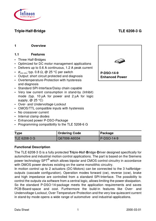
Triple-Half-Bridge TLE 6208-3 G1Overview 1.1Features•Three Half-Bridges•Optimized for DC motor management applications •Delivers up to 0.6 A continuous, 1.2 A peak current •R DS ON ; typ. 0.8 Ω, @25°C per switch•Output: short circuit protected and diagnosis •Overtemperature-Protection with hysteresis and diagnosis•Standard SPI-Interface/Daisy chain capable•Very low current consumption in stand-by (Inhibit)mode (typ. 10µA for power and 2µA for logic supply, @25°C)•Over- and Undervoltage-Lockout•CMOS/TTL compatible inputs with hysteresis •No crossover current •Internal clamp diodes•Enhanced power P-DSO-Package•Programming compatibility to the TLE 5208-6GFunctional DescriptionThe TLE 6208-3 G is a fully protected Tri ple-H alf-B ridge-D river designed specifically for automotive and industrial motion control applications. The part is based on the Siemens power technology SPT ® which allows bipolar and CMOS control circuitry in accordance with DMOS power devices existing on the same monolithic circuitry.In motion control up to 2 actuators (DC-Motors) can be connected to the 3 halfbridge-outputs (cascade configuration). Operation modes forward (cw), reverse (ccw), brake and high impedance are controlled from a standard SPI-Interface. The possibility to control the outputs via software from a central logic, allows limiting the power dissipation.So the standard P-DSO-14-package meets the application requirements and saves PCB-Board-space and cost. Furthermore the build-in features like Over- and Undervoltage-Lockout, Over-Temperature-Protection and the very low quiescent current in stand-by mode opens a wide range of automotive- and industrial-applications.Type Ordering Code Package TLE 6208-3 GQ67006-A9334P-DSO-14-91.2 Pin Configuration (top view)Figure11.3Pin Definitions and FunctionsPin No.Symbol Function1GND Ground; Reference potential; internal connection to pin 7, 8 and 14;cooling tab; to reduce thermal resistance place cooling areas on PCBclose to these pins.2OUT3Halfbridge-Output 3;Internally contected to Highside-Switch 3 and Lowside-Switch 3. TheHS-Switch is a Power-MOS open drain with internal reverse diode;The LS-Switch is a Power-MOS open source with internal reversediode; no internal clamp diode or active zenering;short circuit protected and open load controlled.3V S Power Supply;needs a blocking capacitor as close as possible to GND Value: 22 µFelectrolytic in parallel to 220nF ceramic.5DI Serial Data Input; receives serial data from the control device; serialdata transmitted to DI is an 16bit control word with the LeastSignificant Bit (LSB) being transferred first: the input has an activepull down and requires CMOS logic level inputs;DI will accept data on the falling edge of CLK-signal;see Table Input Data Protocol.4CSN Chip-Select-Not Input; CSN is an active low input; serialcommunication is enabled by pulling the CSN terminal low; CSNinput should only be transitioned when CLK is low; CSN has aninternal active pull up and requires CMOS logic level inputs.6CLK Serial Clock Input; clocks the shiftregister; CLK has an internalactive pull down and requires CMOS logic level inputs.7, 8, 14GND Ground; see pin 1.9DO Serial-Data-Output; this 3-state output transfers diagnosis data tothe control device; the output will remain 3-stated unless the deviceis selected by a low on Chip-Select-Not (CSN);see Table Diagnosis Data Protocol.10INH Inhibit Input; has an internal pull down;device is switched in standby condition by pulling the INH terminallow.11V CC Logic Supply Voltage;needs a blocking capacitor as close as possible to GND;Value: 10 µF electrolytic in parallel to 220nF ceramic.12OUT1Halfbridge-Output 1; see pin 2.13OUT2Halfbridge-Output 2; see pin 2.1.4Functional Block DiagramFigure2Block Diagram1.5Circuit DescriptionFigure 2 shows a block schematic diagram of the module. There are 3 halfbridge drivers on the right-hand side. An HS driver and an LS driver are combined to form a halfbridge driver in each case. The drivers communicate via the internal data bus with the logic and the other control and monitoring functions: undervoltage (UV), overvoltage (OV), overtemperature (TSD), charge pump and fault detect.Two connection interfaces are provided for supply to the module: All power drivers are connected to the supply voltage V S. These are monitored by overvoltage and undervoltage comparators with hysteresis, so that the correct function can be checked in the application at any time.The logic is supplied by the V CC voltage, typ. with 5V. The V CC voltage uses an internally generated Power-On Reset (POR) to initialize the module at power-on. The advantage of this system is that information stored in the logic remains intact in the event of short-term failures in the supply voltage V S. The system can therefore continue to operate following V S undervoltage, without having to be reprogrammed. The “undervoltage”information is stored, and can be read out via the interface. The same logically applies for overvoltage. “Interference spikes” on V S are therefore effectively suppressed.The situation is different in the case of undervoltage on the V CC connection pin. If this occurs, then the internally stored data is deleted, and the output levels are switched to high-impedance status (tristate). The module is initialized by V CC following restart (Power-On Reset=POR).The 16-bit wide programming word or control word (see Table Input Data Protocol) is read in via the DI data input, and this is synchronized with the clock input CLK. The status word appears synchronously at the DO data output (see Table Diagnosis Data Protocol). It is also possible to connect two TLE 6208-3 G in a daisy chain configuration. The DO data output of one device is connected with the DI data input of the second device. In this configuration these two devices are controlled with a single CSN chip select and using a 32-bit wide control word.The transmission cycle begins when the chip is selected with the CSN input (H to L). If the CSN input changes from L to H then the word which has been read in becomes the control word. The DO output switches to tristate status at this point, thereby releasing the DO bus circuit for other uses.The INH inhibit input can be used to cut off the complete module. This reduces the current consumption to just a few µA, and results in the loss of any data stored. The output levels are switched to tristate status. The module is reinitialized with the internally generated POR (Power-On Reset) at restart.This feature allows the use of this module in battery-operated applications (vehicle body control applications).Every driver block from DRV1 to 3 contains a low-side driver and a high-side driver. Both drivers are connected internally to form a half-bridge at the output. This reduction of output pins was necessary to meet the small P-DSO-14 package.When commutating inductive loads, the dissipated power peak can be significantly reduced by activating the transistor located parallel to the internal freewheeling diode. A special, integrated “timer” for power ON/OFF times ensures that there is no crossover current.Input Data Protocol Diagnosis Data ProtocolBIT BIT15OVLO on/off15Power supply fail14not used14Underload13Overcurrent SD on/off13Overload12not used12not used11not used11not used10not used10not used9not used9not used8not used8not used7not used7not used6HS-Switch 36Status HS-Switch 35LS-Switch 35Status LS-Switch 34HS-Switch 24Status HS-Switch 23LS-Switch 23Status LS-Switch 22HS-Switch 12Status HS-Switch 11LS-Switch 11Status LS-Switch 10Status Register Reset0Temp. PrewarningH=ON L=OFF H=ON L=OFFFault Result TableFault Diag.-Bit ResultOvercurrent (load)13Only the failed output is switched OFF. Functioncan be deactivated by bit No. 13.Short circuit to GND (high-side-switch)13Only the failed output is switched OFF. Function can be deactivated by bit No. 13.Short circuit to V S (low-side-switch)13Only the failed output is switched OFF. Function can be deactivated by bit No. 13.Temperature warning0Reaction of control device needed.Temperature shut down (SD)–All outputs OFF.Temperature warning is set before.Underload/Openload14Reaction of control device needed. Undervoltage lockout(UVLO)15All outputs OFF.Overvoltage lockout (OVLO)15All outputs OFF.Function can be deactivated by bit No. 15.H=failure;L=no failure.Note:Stresses above those listed here may cause permanent damage to the device.Exposure to absolute maximum rating conditions for extended periods may affect device reliability.2Electrical Characteristics 2.1Absolute Maximum RatingsParameterSymbolLimit Values UnitRemarksmin.max.Voltages Supply voltage V S – 0.340V –Supply voltage V S – 1–V t < 0.5 s; I S > – 2 A Logic supply voltage V CC – 0.3 5.5V 0 V < V S < 40 V Logic input voltages (DI, CLK, CSN, INH)V I – 0.3 5.5V 0 V < V S < 40 V 0 V < V CC < 5.5 V Logic output voltage (DO)V DO – 0.3 5.5V 0 V < V S < 40 V 0 V < V CC < 5.5 V Output voltage (OUT 1-3)V OUT– 0.340V0 V < V S < 40 VCurrentsOutput current (cont.)I OUT1-3––A internal limited Output current (peak)I OUT1-3––Ainternal limitedLimit is mentioned in the overcurrent section of operating range Temperatures Junction temperature T j – 40150°C –Storage temperatureT stg– 50150°C–2.2Operating RangeParameter Symbol Limit Values Unit Remarksmin.max.Supply voltage V S V UV OFF40V After V S risingabove V UV ON Supply voltage slew rate d V S /d t–10V/µs–Logic supply voltage V CC 4.75 5.50V–Supply voltage increasing V S– 0.3V UV ON V Outputs in tristate Supply voltage decreasing V S– 0.3V UV OFF V Outputs in tristateLogic input voltage (DI, CLK, CSN, INH)VI– 0.3V CC V–SPI clock frequency f CLK–1MHz–Junction temperature T j– 40150°C–Thermal ResistancesJunction pin R thj-pin–30K/W measured topin 1, 7, 8, 14 Junction ambient R thjA–65K/W–Note:In the operating range, the functions given in the circuit description are fulfilled.2.3Electrical Characteristics8V<V S< 40V; 4.75V<V CC<5.25V; INH=High; all outputs open; –40°C<T j<150°C; unless otherwise specifiedParameter Symbol Limit Values Unit Test Conditionmin.typ.max.Current ConsumptionQuiescent current I S–820µA INH= Low;VS = 13.2VTj= 25°C Quiescent current I S––30µA INH= Low;VS= 13.2V; Logic-Supply current I CC–210µA INH = Low Logic-Supply current I CC–12mA SPI not active Supply current I S–25mA–Over- and Under-Voltage LockoutUV-Switch-ON voltage V UV ON– 6.57V V S increasing UV-Switch-OFF voltage V UV OFF 5.6 6.1 6.6V V S decreasing UV-ON/OFF-Hysteresis V UV HY–0.4–V V UV ON–V UV OFF OV-Switch-OFF voltage V OV OFF343740V V S increasing OV-Switch-ON voltage V OV ON303336V V S decreasing OV-ON/OFF-Hysteresis V OV HY–4–V V OV OFF–V OV ONOutputs OUT1-3Static Drain-Source-On Resistance Source (High-Side) I OUT = –0.5AR DS ON H–0.80.95Ω8V <V S < 40VT j = 25 °C– 1.6Ω8V <V S < 40V 1–ΩV S OFF < V S ≤8VT j = 25°C –2ΩV S OFF < V S ≤8V Sink (Low-Side)I OUT = 0.5AR DS ON L–0.750.9Ω8V <V S < 40V T j = 25 °C– 1.5Ω8V <V S < 40V 1–ΩV S OFF < V S ≤8V T j = 25 °C–2ΩV S OFF < V S ≤8VLeakage CurrentSource-Output-Stage 1 to 3I QLH –5–1–µA V OUT1-3= 0V Sink-Output-Stage 1 to 3I QLL–150300µAV OUT1-3= V SOvercurrentSource shutdown threshold I SDU –2–1.3–1A –Sink shutdown threshold I SDL 1 1.22A –Current limit I OCL – 2.44A sink and source Shutdown delay timet dSD102840µssink and source2.3Electrical Characteristics (cont ’d)8V <V S < 40V; 4.75V <V CC <5.25V; INH =High; all outputs open; –40°C <T j <150°C;unless otherwise specifiedParameter Symbol Limit Values Unit Test Conditionmin.typ.max.2.3Electrical Characteristics (cont’d)8V<V S< 40V; 4.75V<V CC<5.25V; INH=High; all outputs open; –40°C<T j<150°C; unless otherwise specifiedParameter Symbol Limit Values Unit Test Conditionmin.typ.max.Open Circuit/Underload DetectionDetection current I OCD153045mA–Delay time t dOC200370600µs–Output Delay Times; V S = 13.2V;R Load= 25 Ω (device not in stand-by for t > 1 ms) Source ON t d ON H–820µs–Source OFF t d OFF H–420µs–Sink ON t d ON L–720µs–Sink OFF t d OFF L–320µs–Dead time t D HL13–µs t d ON L–t d OFF H Dead time t D LH15–µs t d ON H–t d OFF LOutput Switching Times; V S = 13.2V;R Load= 25 Ω (device not in stand-by for t> 1 ms) Source ON t ON H–520µs–Source OFF t OFF H–25µs–Sink ON t ON L– 2.010µs–Sink OFF t OFF L– 1.55µs–Clamp Diodes Forward VoltageUpper V FU–0.9 1.3V I F = 0.5 A Lower V FL–0.9 1.3V I F = 0.5 AInhibit InputH-input voltage threshold V IH –0.520.7V CC –L-input voltage threshold V IL 0.20.48–V CC–Hysteresis of input voltage V IHY 50200500mV –Pull down current I I 525100µA V I = 0.2 × V CC Input capacitanceC I–1015pF0V < V CC <5.25 VNote:Capacitances are guaranteed by design.SPI-InterfaceDelay Time from Stand-by to Data In/Power on Reset Setup timet set––100µs –Logic Inputs DI, CLK and CSN H-input voltage thresholdV IH –0.520.7V CC–L-input voltage thresholdV IL 0.20.48–V CC–Hysteresis of input voltage V IHY50200500mV –Pull up current at pin CSNI ICSN –50–25–10µA V CSN = 0.7 × V CC Pull down current at pin DI I IDI 102550µA V DI = 0.2 × V CC Pull down current at pin CLK I ICLK 102550µA V CLK = 0.2 × V CC Input capacitance at pin CSN, DI or CLKC I–1015pF0V < V CC <5.25 VNote:Capacitances are guaranteed by design.2.3Electrical Characteristics (cont ’d)8V <V S < 40V; 4.75V <V CC <5.25V; INH =High; all outputs open; –40°C <T j <150°C;unless otherwise specifiedParameter Symbol Limit Values Unit Test Conditionmin.typ.max.Logic Output DOH-output voltage level V DOH V CC– 1.0VCC– 0.7–V I DOH=1 mAL-output voltage level V DOL–0.20.4V I DOL= –1.6 mA Tri-state leakage current I DOLK– 10010µA V CSN =V CC0V<V DO < V CC Tri-state input capacitance C DO–1015pF V CSN=V CC0V<V CC <5.25 VNote:Capacitances are guaranteed by design.Data Input TimingClock period t pCLK1000––ns–Clock high time t CLKH500––ns–Clock low time t CLKL500––ns–Clock low before CSN low t bef500––ns–CSN setup time t lead500––ns–CLK setup time t lag500––ns–Clock low after CSN high t beh500––ns–DI setup time t DISU250––ns–DI hold time t DIHO250––ns–Input signal rise timeat pin DI, CLK and CSN trIN––200ns–Input signal fall timeat pin DI, CLK and CSN tfIN––200ns–2.3Electrical Characteristics (cont’d)8V<V S< 40V; 4.75V<V CC<5.25V; INH=High; all outputs open; –40°C<T j<150°C; unless otherwise specifiedParameter Symbol Limit Values Unit Test Conditionmin.typ.max.Data Output Timing DO rise time t rDO –50100ns C L = 100 pF DO fall time t fDO –50100ns C L = 100 pFDO enable time t ENDO – –250ns low impedance DO disable time t DISDO – –250ns high impedanceDO valid timet VADO–100250nsV DO < 0.2 V CC ;V DO > 0.7 V CC ; C L = 100 pFThermal Prewarning and Shutdown Thermal prewarning junction temperatureT jPW 120145170°C –Temperature prewarning hysteresis∆T–30–K –Thermal shutdown junction temperatureT jSD 150175200°C –Thermal switch-on junction temperatureT jSO120–170°C –Temperature shutdown hysteresis ∆T–30–K –Ratio of SD to PW temperatureT jSD /T jPW 1.051.20–––Note:Temperatures are guaranteed by design.The listed characteristics are ensured over the operating range of the integrated circuit. Typical characteristics specify mean values expected over the production spread. If not otherwise specified, typical characteristics apply at T A = 25°C and the given supply voltage.2.3Electrical Characteristics (cont ’d)8V <V S < 40V; 4.75V <V CC <5.25V; INH =High; all outputs open; –40°C <T j <150°C;unless otherwise specifiedParameter Symbol Limit Values Unit Test Conditionmin.typ.max.3Timing DiagramsFigure3Data Transfer TimingFigure4Timing for Temperature Prewarning onlyFigure5SPI-Input TimingFigure6 Turn OFF/ON TimeFigure7DO Valid Data Delay Time and Valid TimeFigure8DO Enable and Disable TimeFigure9Application Circuit。
UTCBA6208中文资料
UTC BA6208LINEAR INTEGRATED CIRCUITUTC UNISONIC TECHNOLOGIES CO., LTD.1QW-R109-004,AREVERSIBLE MOTOR DRIVERDESCRIPTIONThe UTC BA6208 is monolithic ICs used for driving reversible motors. They allow control of reversible motors in cassette players and other electrical equipment by using TTL-level logic signals. The ICs contain a logic section, which controls forward and reverse rotations as well as forced stop, and an output power section, which can supply an output current of up to 100mA (typical) according to the logic control.FEATURES*Motor driving power transistors are built in (100mA typically).*Brake is applied when stopping the motor (when in- puts A and B are both HIGH level).*Built-in diode to absorb surge currents.*Very low standby circuit current when inputs A and B are both LOW level.*Wide range of operating supply voltage (4.5 ~ 15.0V) *Direct control with the TTL logic.ABSOLUTE MAXIMUM RATING (Ta=25°C)PARAMETERSYMBOL VALUEUNITPower Supply Voltage Vcc 18V Power Dissipation Pd 700 (SIP9) [note 1] 450 (SOP8) [note 2]mW mW Operating Temperature Topr -20 to +60 °C Storage Temperature Tstg -55 to +125°C Maximum Output CurrentIout500mANote 1: Reduced by 7mW for each increase in Ta of 1°C over 25°C. Note 2: Reduced by 4.5mW for each increase in Ta of 1°C over 25°C.RECOMMENDED OPERATING CONDITIONS (Ta=25°C)PARAMETERSYMBOL MINTYP MAX UNITPower Supply Voltage Vcc4.515VUTC BA6208LINEAR INTEGRATED CIRCUITUTC UNISONIC TECHNOLOGIES CO., LTD.2QW-R109-004,AINPUT TRUTH TABLE3pin (Ain)2pin (Bin)8pin (Aout)7pin (Bout)H L H L L H L H H H L L L L OPEN OPENNote: HIGH level input is 2.0V or more. LOW level input is 0.8V or less.ELECTRICAL CHARACTERISTICS (Ta=25°C, V CC =9V, unless otherwise specified)PARAMETER SYMBOL TEST CONDITIONS MIN TYP MAX UNITOutput CurrentI O 200 mA Output Saturation Voltage V CE Io =100mA 1.6 V Input High Level Voltage V IH2.0 V Input Low Level Voltage V IL0.8VStandby Supply Current I ST When inputs A and B areboth Low level0.4 mAInput High Level CurrentI IHV IH =4.5V 400µA Note: A diode that absorbs at least 500mA is built in to give protection against surge currents with a pulse width of 10 ms and a duty ratio of 10% or less.UTC BA6208LINEAR INTEGRATED CIRCUITUTC UNISONIC TECHNOLOGIES CO., LTD.3QW-R109-004,ATEST CIRCUIT。
HP6208
� 散热要求
尽管电路具有较高的转换效率,芯片内部 仍会消耗一定的功率,对于一个典型的功率开 关而言,应使用必要的散热措施,以避免过高 的温度导致热保护或性能下降。IC内部主要的 发热是开关管的开关损耗产生的热量,因此恰 当的散热位置通过IC的Pin7-8脚,一个易于使 用的方法是在Pin7-8脚铺设一定面积的PCB铜 箔,必要时将铜箔镀锡处理将大大增加散热能 力。对于一个85-265V输入,12W输出的典型应 用,200mm2的以上的铜箔面积是必要的。
振荡器部分
符号 Fs ΔFsv ΔFsT FsBack 说明 振荡频率 频率随电压变化率 频率随温度变化率 频率回转范围 Vcc=5-9V Ta=0-85℃ 测试条件 最小 典型 65 2
HP6208
最大 1 1 单位 kHz % % %
PWM部分
符号 DMIN DMAX 说明 最小开通占空比 最大开通占空比 测试条件 VFB=0V VFB>4.5V 55 最小 典型 1.5 60 65 最大 单位 % %
第 5 页
深圳市海汇鸿芯业电子有限公司
应用信息
� 启动部分
在系统启动期间芯片仅需从VIN端输入极 小的触发电流即可打开内部高压电流源电路, 实现系统快速充电启动, 因此仅需要极小的VIN 电阻即可满足电路启动需要,这大大减小了电 阻本身的功耗进一步降低了整机的待机功耗。 在一般的应用中可以使用4.7-10Meg.的电 阻作为VIN电阻。 因VIN电阻长期承受输入直流高压, 应用中 应确保电阻耐压能力满足要求,一个较好的做 法是使用两个电阻串联使用,例如两个1206型 电阻串联。
Ta=25℃,Vcc=7.5V, Rs=1Ω)
测试条件 VCC=0V,IHV=1mA IHV=800mA CL=1nF CL=1nF Lp=1.2mH RVIN=4.7Meg.Ω
手机电池型号表

Nokia 6208c 说明书
通话........................................................................17
拨打电话...........................................................................17 来电...................................................................................17 单键拨号...........................................................................17 声控拨号...........................................................................17 通话中选项........................................................................17
关于您的设备......................................................................8 网络服务.............................................................................8 密码功能.............................................................................8 配置设置服务......................................................................9 下载内容.............................................................................9 友情提示...............................................9 软件更新.............................................................................9 诺基亚支持........................................................................10 数字版权管理....................................................................10 键盘锁...............................................................................15 未插入 SIM 卡时可以使用的功能......................................16
6208轴承6208轴承参数
6208轴承深沟球轴承6208轴承经销无锡特瑞恩0510-********单列深沟球轴承6208轴承尺寸内径40mm外径80mm厚度18mm深沟球轴承6208轴承特点深沟球轴承结构简单,使用方便,是应用范围最广的一类轴承。
它主要用以承受径向载荷,也可承受一定的轴向载荷。
当轴承的径向游隙加大时,具有角接触球轴承的功能,可承受教大的轴向载荷。
与尺寸相同的其他类轴承比较,此类轴承摩擦因数小,极限转速高。
在转速较高不宜采用推力球轴承的情况下可用该类轴承承受轴向载荷。
6208轴承深沟球轴承具体分类及型号对照:1、开式深沟球轴承(60000型)注:主要用以承受径向载荷,也可承受较小的轴向载荷,轴的轴向位移限制在轴向游隙范围内允许内圈相对外圈倾斜.1 - */12、外圈有止动槽的深沟球轴承(60000 N型)注:同基型深沟球轴承装入止动环可简化轴承在轴承座孔内轴向定位3、一面带防尘盖,另一面外圈有止动槽的深沟球轴承(60000-ZN型)4、两面带防尘盖,外圈有止动槽的深沟球轴承(60000-2ZN型)5、一面带防尘盖的深沟球轴承(60000-Z)6、两面带防尘盖的深沟球轴承(60000-2Z)注:同基型深沟球轴承防尘盖与内圈挡边之间有间隙,极限转速与开式深沟球轴承相同,密封较好轴承在装配时填入了适量润滑剂,安装使用时不用清洗和添加润滑剂。
7、一面带密封圈的深沟球轴承(60000-RS型、60000-RZ型)注:同基型深沟球轴承密封圈与内圈挡边有接触式(后置代号%/,(./ )和非接触式(.#,(.#),接触式密封效果好,但摩擦阻力大,极限转速低。
8、两面带密封圈的深沟球轴承(60000-2RS型、60000-2RZ型)注:非接触式密封极限转速与开式深沟球轴承相同轴承在装配时填入适量润滑剂安装使用时不用清洗和添加润滑剂。
9、凸缘外圈深沟球轴承(F60000型)10、一面带防尘盖的凸缘外圈深沟球轴承(F60000-Z型)11、两面带防尘盖的凸缘外圈深沟球轴承(F60000-2Z型)2、6208轴承6208ZZ轴承6208Z轴承6208LLU轴承6208-2RS轴承6208.2RSR.C3轴承6208NR轴承6208DDU轴承6208-2Z/C3轴承6208轴承查询了解更多轴承库存信息及最新报价请联系我们。
我的字,我的气质——NOKIA 6208c
我的字,我的气质——NOKIA 6208c
佚名
【期刊名称】《数码》
【年(卷),期】2009(000)002
【摘要】在诺基亚跨年新品发布会上.诺基亚带来了一款具备手写输入功能的全新手机——诺基亚6208c.这款手机也是继诺基亚6108、诺基亚3108等手写手机之后,由诺基亚中国工程师专为中国手机用户开发、设计的产品。
诺基亚6208c支持用户在输入中文信息时任意切换手写输入和键盘输入方式,易学易用.提高信息沟通效率。
【总页数】1页(P118)
【正文语种】中文
【中图分类】TN929.53
【相关文献】
1.Nokia进军Netbook瀚字博德、金像电子受惠 [J],
2.新背剑武士诺基亚6208c [J],
3.今非昔“笔”:NOKIA 6208C [J],
4.诺基亚6208c [J],
5.NOKIA 6208c 扬剑出鞘 [J],
因版权原因,仅展示原文概要,查看原文内容请购买。
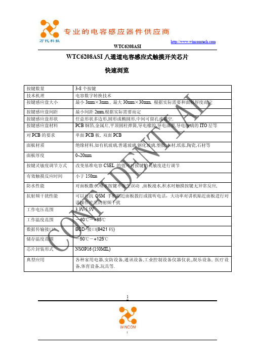
WTC6208ASI
6.2.1 选择合适的电容 Csel.....................................................................................10
6.2.2 感应盘面积.....................................................................................................10
工作电压范围 工作温度范围 数据传输接口 储存温度范围 芯片封装形式 典型应用
3-8 个按键 电容数字转换技术 最小 3mm×3mm , 最大 30mm×30mm, 根据实际需要和面板厚度而定 最小间距 2mm,根据实际需要而定 任意形状多边形,圆形或椭圆形,中间可留孔或镂空. PCB 铜箔,金属片,平顶圆柱弹簧,导电橡胶,导电油墨,导电玻璃的 ITO 层等 单面 PCB 板, 双面 PCB
绝缘材料,如有机玻璃,普通玻璃,钢化玻璃,塑胶,木材,纸张,陶瓷,石材等
0~20mm
改变基准电容 CSEL 的值可对按键的灵敏度进行调节
小于 150ms 对面板撒水,喷水按键不发生误动 ,面板漫水,积水时触摸按键无异常反应,
可以对抗 GSM 手机贴近面板拨打或接听电话,大功率对讲机贴近面板进行对 讲操作产生的射频干扰 3.3V-5.5V
5 输出指示............................................................................................................................................................. 8 5.1 BCD 接口输出时序图 .................................................................................................8 5.2 BCD 输出的真值表 ....................................................................................................8
- 1、下载文档前请自行甄别文档内容的完整性,平台不提供额外的编辑、内容补充、找答案等附加服务。
- 2、"仅部分预览"的文档,不可在线预览部分如存在完整性等问题,可反馈申请退款(可完整预览的文档不适用该条件!)。
- 3、如文档侵犯您的权益,请联系客服反馈,我们会尽快为您处理(人工客服工作时间:9:00-18:30)。
一、二级维修中心人员进行任何私自的硬件焊接维修或者越权更换配件都可能造 成客户手机保修失效,最终影响客户利益。所带来的损失也将由维修中心人员自 己承担。
频带: GSM三频:900MHz/1800MHz/1900MHz
显示屏: LCD: 2.4寸 QVGA (240x320 像素),1670万色TFT
照相机: 320万像素,自动对焦,8倍数码变焦, 双LED闪光灯
操作系统: S40
连接: 无线:蓝牙2.0(支持立体声) 接口:Micro USB 接口,3.5mm AV接口 机身内存13M,最大支持8GB Micro SD 手写板阻抗匹配问题造成VDD电压波动大,从而 计算错误,尽量更换阻值相同的手写板,建议增 加X+ Y+端电容试验。
中间间隔物点距或材质造成手写时接触的位置过 多,更换好质量的触摸解决。
校准时无法通过,建议格式化,消除前触摸板的 起始---终止坐标的记忆,重新建立绝对位置数 据(也跟阻抗有关系)。
Betty(N2300): BB5第二个能量管理器,功能如下: 产生核心电压(VCORE) 充电控制电路 电平转换器和给USB/FBUS调压器 电池电流测量的计流器 外部背景灯的驱动控制接口 数字接口(CBUS)
© 2008 Nokia
3、主要元器件简介
TMX320DM5012ZAN(N1400) 照相机硬件加速器,负责管理照相功能。与6210s一样。
结构,通常是玻璃。
•
缺点:电阻触摸屏的多层结构会导致很大的光损
失,对于手持设备通常需要加大背光源来弥补透
光性不好的问题,但这样也会增加电池的消耗。
•
优点:电阻式触摸屏它的屏和控制系统都比较便
宜,反应灵敏度也很好。
© 2008 Nokia
附:触摸屏知识简介
Y座标采集简化示意图
© 2008 Nokia
照相机接口电路:
© 2008 Nokia
5、照相机电路原理
闪光灯电路:
该电路使用了与3600s、6210s、n79、n85、5800等相同的闪光灯驱动IC。
© 2008 Nokia
6、主板元件及 主要信号测量点
© 2008 Nokia
6、主板元件及 主要信号测量点
© 2008 Nokia
7、说明
TSC2004(N2450) 触摸屏控制IC。与5800一样。
LP3929TMEX(N3200) 存储卡电平转换IC,负责卡供电和电平转换。与5220、3600s、7310s、5130、N78等一样。
RF IC(N1001) BB5射频芯片,它集成了VCO,VCTCXO,滤波器等所有外围器件。 使用这种结构的如5310、3600s、5130等。
China Care/Go To Market
6208c硬件介绍
HMX
2009年5月
1
主要内容
1、手机参数 2、产品框图 3、主要元器件简介 4、触摸屏控制电路原理 5、照相机电路原理 6、主板元件及主要信号测量点 7、说明 附:触摸屏知识简介
© 2008 Nokia
1、手机参数
FEM(N1002) BB5的前端模块,集成了双工、功放等电路。 使用这种结构的如5310、3600s、5130等。
© 2008 Nokia
4、触摸屏控制电路原理
PINTDAV低电平时发起触摸请求
© 2008 Nokia
5、照相机电路原理
供电电路:
© 2008 Nokia
5、照相机电路原理
Thanks! Q&A?
© 2008 Nokia
埃=10-10米)以下时会突然变得透明,透光率为80%,再薄下去透光率反而下降,到300埃厚度 时又上升到80%。 通过调整铟和锡的比例,沉积方法,氧化程度以及晶粒的大小可以调整这种物质的性能。薄的ITO 材料透明性好,但是阻抗高;厚的ITO材料阻抗低,但是透明性会变差。在PET聚脂薄膜上沉积时 ,反应温度要下降到150度以下,这会导致ITO氧化不完全,之后的应用中ITO会暴露在空气或空气 隔层里,它单位面积阻抗因为自氧化而随时间变化。这使得电阻式触摸屏需要经常校正。 ITO是所有电阻技术触摸屏及电容技术触摸屏都用到的主要材料,实际上电阻和电容技术触摸屏的 工作面就是ITO涂层。
© 2008 Nokia
附:触摸屏知识简介
按照触摸屏的工作原理和传输信息的介质,触摸屏大致分为四种: 1、电阻式触摸屏 2、电容式触摸屏 3、红外线式触摸屏 4、声表面波式触摸屏
电阻屏的核心------ITO ITO是铟(yin)锡氧化物的英文缩写,它是一种透明的弱导电体,特性是当厚度降到1800个埃(1
© 2008 Nokia
附:触摸屏知识简介
•
电阻式触摸屏结构:
•
手指触摸的表面是一个硬涂层,用以保护下面的
PET层。PET层是很薄的有弹性的PET薄膜,当表面
被触摸时它会向下弯曲,并使得下面的两层ITO涂
层能够相互接触并在该点连通电路。两个ITO层之
间是约千分之一英寸厚的一些隔离支点使两层分
开。最下面是一个透明的硬底层用来支撑上面的
电阻式触摸屏工作原理:
由软件控制,启动连续数据采集过程,每一个 点的数据采集两次,首先将VDD加到Y+ Y-端,然 后通过X+采集电压数据,通过A/D转换计算出Y做 标,然后将VDD加到X+ X-端,然后通过Y+采集电 压数据,通过A/D转换计算出X座标,从而得到准确
的点,通过一组点计算出路线,再根据不同的界 面得到不同的反馈结果-----写字 或 控制等等。
该处理器的工作条件: 电压:
VCORE=1.35V(Local模式),来自于Betty,休眠模式下降为1.05V VIO=1.8V,来自于Avilma VRFC=1.8V,来自于Avilma(启动后)
时钟: RFCLK=38.4MHz系统时钟,来自于射频IC SLEEPCLK=32.768KHz休眠时钟,来自于Avilma
• 使用BL-4S 锂电池 • 通话时间上限约为3.5小时, 待机时间上限约为300小时(基于网络条件)
© 2008 Nokia
2、产品框图
© 2008 Nokia
3、主要元器件简介
RAPS(D2800): 核心处理器,S表示存储器是焊接在RAP之上。 (使用这种处理器的如5310、5220、3600s、5130、7310s等)
© 2008 Nokia
3、主要元器件简介
Avilma(N2200):BB5主能量管理器,功能如下: 开机逻辑和复位控制 充电器的检测和电池电压监测 32K时钟和外部振荡器 实时时钟和外部备用电池 UI接口包括SIM卡接口,振子控制 A/D、D/A转换器 调压器(VRCP1、VSIM1、 VSIM2、VRFC、VR1、VIO、VDRAM、VAUX、VANA、VREF) 数字接口(CBUS)