DP8261中文版
华特自动链接设备兼容性指南说明书
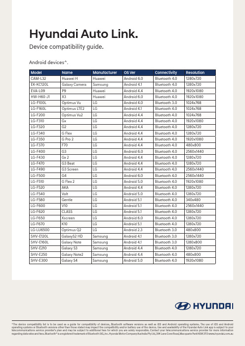
2560x1440
iOS devices^.
Model A1429 A1586 A1522 A1660
Name iPhone5 iPhone6 iPhone6+ iPhone7
Manufacturer Apple Apple Apple Apple
OS Ver 8.1.3 10.2.1 10.2.1 10.2.1
Connectivity Bluetooth 4.2 Bluetooth 4.2 Bluetooth 4.2 Bluetooth 4.2
Resolution 1136x640 1334x750 1920x1080 1334x750
Guide current as at 17 May2017.
Samsung
Galaxy S4 Zoom Samsung
Galaxy On7
Samsung
Galaxy ALPHA Samsung
Galaxy S5
Samsung
Galaxy S6
Samsung
Galaxy S6 Edge+ Samsung
Galaxy J5 2016 Samsung
Galaxy Note3 Neo
Connectivity Bluetooth 4.0 Bluetooth 4.0 Bluetooth 4.0 Bluetooth 4.0 Bluetooth 3.0 Bluetooth 4.0 Bluetooth 4.0 Bluetooth 4.0 Bluetooth 4.0 Bluetooth 4.0 Bluetooth 4.0 Bluetooth 4.0 Bluetooth 4.0 Bluetooth 4.0 Bluetooth 4.0 Bluetooth 4.0 Bluetooth 4.0 Bluetooth 4.0 Bluetooth 4.0 Bluetooth 4.0 Bluetooth 4.0 Bluetooth 4.0 Bluetooth 4.0 Bluetooth 4.0 Bluetooth 4.0 Bluetooth 3.0 Bluetooth 3.0 Bluetooth 3.0 Bluetooth 4.0 Bluetooth 4.0 Bluetooth 4.0
RC6621D 低功耗蓝牙(BLE)透传协议数据手册说明书

RC6621DQ低功耗蓝牙透传模块数据手册文档信息型号RC6621D备注名称低功耗蓝牙透传模块文档类型数据手册文档编号RCBM-H02版本日期V2.0.02020-10-18版本更新版本号文档日期更新内容V2.0.02020/10/18 第一次发布;注:本文档讲不定期更新,在使用此文档前,请确保为最新版本。
文档中的信息仅供深圳市智汉科技有限公司RF Crazy®的授权用户或许可人使用。
没有深圳市智汉科技有限公司RF Crazy®的书面授权,请勿将本文档或其他部分内容印制或者作为电子文档副本传播。
目录1.产品概述 (1)主要特点 (1)模式默认配置 (2)设备状态 (2)2.工作模式示意图 (3)3.模块尺寸及引脚 (3)4.串口透传协议说明 (5)5.BLE协议说明(APP接口) (5)Service UUID (5)BLE数据接收UUID (5)BLE数据发送UUID (6)AT指令操作UUID (6)6.AT指令 (6)AT命令表 (7)进入AT指令模式 (7)退出AT指令模式 (8)设备名称 (8)MAC地址 (8)串口回显 (9)显示设备状态 (9)广播参数 (10)连接间隔 (10)Service (11)断开连接 (12)自定义广播内容 (12)发射功率 (13)休眠模式 (14)串口波特率 (14)用户鉴权 (15)设备重启 (16)恢复出厂设置 (16)固件版本查询 (16)7.用APP测试透传功能 (16)8.IOS APP编程参考 (19)9.主机(MCU)参考代码(透传) (20)10.使用条件及注意事项 (21)联系我们................................................................................................错误!未定义书签。
附录A:BLE模块应用方案提示. (24)附录B:模块射频参数测试报告 (25)附录C:功耗测试截图 (37)1.产品概述智汉科技RF Crazy®RC6621DQ是基于OnMicro的HS6621D SoC设计开发的高性能、高灵敏、低成本的蓝牙5.2(BLE)模块。
S8261和DW01-8205A主流锂电池保护板原理图说明
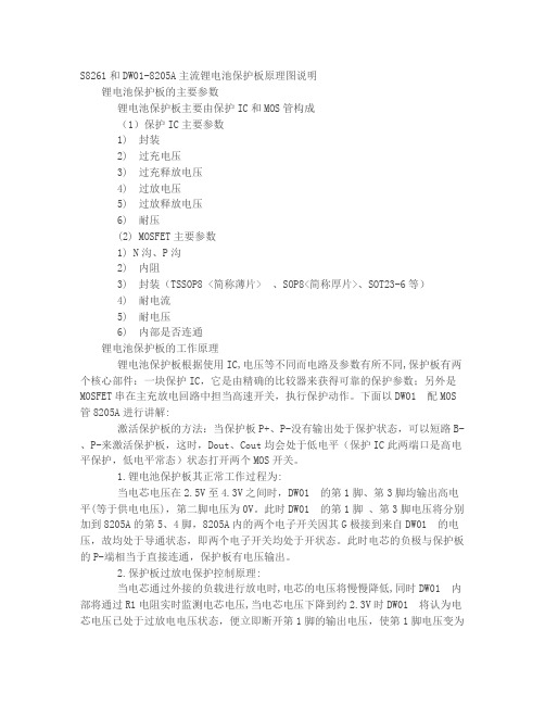
S8261和DW01-8205A主流锂电池保护板原理图说明锂电池保护板的主要参数锂电池保护板主要由保护IC和MOS管构成(1)保护IC主要参数1) 封装2) 过充电压3) 过充释放电压4) 过放电压5) 过放释放电压6) 耐压(2) MOSFET主要参数1) N沟、P沟2) 内阻3) 封装(TSSOP8 <简称薄片> 、SOP8<简称厚片>、SOT23-6等)4) 耐电流5) 耐电压6) 内部是否连通锂电池保护板的工作原理锂电池保护板根据使用IC,电压等不同而电路及参数有所不同,保护板有两个核心部件:一块保护IC,它是由精确的比较器来获得可靠的保护参数;另外是MOSFET串在主充放电回路中担当高速开关,执行保护动作。
下面以DW01 配MOS 管8205A进行讲解:激活保护板的方法:当保护板P+、P-没有输出处于保护状态,可以短路B-、P-来激活保护板,这时,Dout、Cout均会处于低电平(保护IC此两端口是高电平保护,低电平常态)状态打开两个MOS开关。
1.锂电池保护板其正常工作过程为:当电芯电压在2.5V至4.3V之间时,DW01 的第1脚、第3脚均输出高电平(等于供电电压),第二脚电压为0V。
此时DW01 的第1脚、第3脚电压将分别加到8205A的第5、4脚,8205A内的两个电子开关因其G极接到来自DW01 的电压,故均处于导通状态,即两个电子开关均处于开状态。
此时电芯的负极与保护板的P-端相当于直接连通,保护板有电压输出。
2.保护板过放电保护控制原理:当电芯通过外接的负载进行放电时,电芯的电压将慢慢降低,同时DW01 内部将通过R1电阻实时监测电芯电压,当电芯电压下降到约2.3V时DW01 将认为电芯电压已处于过放电电压状态,便立即断开第1脚的输出电压,使第1脚电压变为0V,8205A内的开关管因第5脚无电压而关闭。
此时电芯的B-与保护板的P-之间处于断开状态。
CXP82612中文资料
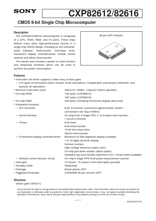
PE0/INT0/ EC0 PE1/INT1 PE2/INT2 PE3/INT3/ NMI PE4/RMC PE5 PE6 PE7/TO/ ADJ
I/O
Functions
I/O/Analog Input
(Port A) 8-bit I/O port. I/O can be set in a bit unit. Incorporation of pull-up resistor can be set through the software in a unit of 4 bits. (8 pins)
Structure Silicon gate CMOS IC
Sony reserves the right to change products and specifications without prior notice. This information does not convey any license by any implication or otherwise under any patents or other right. Application circuits shown, if any, are typical examples illustrating the operation of the devices. Sony cannot assume responsibility for any problems arising out of the use of these circuits.
(Port B) 8-bit I/O port. I/O can be set in a bit unit. Incorporation of pull-up resistor can be set through the software in a unit of 4 bits. (8 pins)
MX-826中文资料
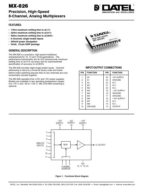
FEATURES•170ns maximum settling time to ±0.1%•225ns maximum settling time to ±0.01%•400ns maximum settling time to ±0.003%•8 Channels single-ended inputs •395mW power dissipation •Small, 24-pin DDIP packageGENERAL DESCRIPTIONThe MX-826 is a precision, high-speed multiplexercharacterized for 10, 12 and 14-bit applications. Theperformance benchmarks are its 225 nanoseconds maximum settling time to ±0.01% accuracy and its unprecedented specification of accuracy to ±0.003%.The MX-826 provides eight single-ended inputs. Channel addressing is done by a three-bit binary code and break-before-make switching assures that no two channels are ever momentarily shorted together.The MX-826 operates from ±15V and +5V power supplies.Models are available in two operating temperature ranges:0 to +70°C and –55 to +125°C. MIL-STD-883 screening is optional.PINFUNCTION PIN FUNCTION 1A024+5V SUPPLY 2A123GROUND 3A222N.C.4IN121N.C.5IN220N.C.6IN319–15V SUPPLY 7IN418GROUND 8IN517GROUND9IN616+15V SUPPLY 10IN715N.C.11IN814N.C.12GROUND13OUTPUTMX-826Precision, High-Speed8-Channel, Analog MultiplexersINNOVATION and EX C E LL E N C E®®Figure 1. Functional Block DiagramINPUT/OUTPUT CONNECTIONS456789101112, 17, 18, 2313OUTPUT+15V SUPPLY +5V SUPPLY ANALOG INPUTS CHANNEL ADDRESS15V SUPPLY DATEL, Inc., Mansfield, MA 02048 (USA) • Tel: (508) 339-3000, (800) 233-2765 Fax: (508) 339-6356 • Email: sales@ • Internet: 元器件交易网®®MX-826POWER REQUIREMENTS MIN TYP MAX UNITS Range+15V Supply +14.5+15+15.5Volts –15V Supply –14.5–15–15.5Volts +5V Supply+4.75+5+5.25Volts Current (Quiescent)+15V Supply —+13+21mA –15V Supply —–13–21mA +5V Supply—<1+1mA Power Supply Rejection Ratio 86——dB Power Dissipation—395575mWPHYSICAL/ENVIRONMMENTAL Operating Temp. Range, Case MC Model 0—+70°C MM Model–55—+125°C Storage Temp. Range –65—+150°CPackage Type 24-pin, metal-sealed, ceramic DDIPWeight0.42 oz. (12 grams)ABSOLUTE MAXIMUM RATINGSPARAMETERSLIMITS +15V Supply, Pin 160 to +18V –15V Supply, Pin 190 to –18V +5V Supply, Pin 24–0.5 to +7V Digital Inputs, Pins 1, 2, 3–0.3 to +5.5V Analog Inputs, Pins 4-11–15 to +15V Lead Temperature (10s)300°C Short Circuit to Ground , Pin 13ContinuousFUNCTIONAL SPECIFICATIONS(Apply over the operating temperature range and over the operating power supply range unless otherwise specified.)INPUTSMIN.TYP .MAX.UNITS Input Voltage Range±10±10.5—Volts Digital Input, Logic Levels Logic 1+2.0——Volts Logic 0——+0.8Volts Logic Loading Logic 1——+10µA Logic 0——–10µAOUTPUTSOutput Range ±10.0±10.5—Volts Output Current±15——mA Stable Capacitive Load 100——pF Output Impedance DC —0.1—OhmsPERFORMANCE Gain—–1—V/V Gain Error, 25°C ——±0.03%FS Gain Tempc o –55 to +125°C —±0.5±5ppm/°C Offset, 25°C—±0.1±0.5mV Offset Voltage Drift —<5±15µV/°C Slew Rate ±250±300—V/µs Cross Talk 100kHz —–90–83dB 1MHz —–80–75dB Bandwidth3dB Small Signal 88.5—MHz Full Power 3 4.5—MHz Input Impedance 2.45 2.5 2.55k ΩOutput Settling Time(10V step, +25°C) 500Ω Load ±0.1% 10 Bits —100170ns ±0.01% 12 Bits —150225ns ±0.003% 14 Bits—300400ns (20V step, + 25°C) 1k Ω Load ±0.1% 10 Bits —150200ns ±0.01% 12 Bits —200300ns ±0.003% 14 Bits—600720ns Switching Characteristics Break-Before-Make Delay 81525ns Turn On Time —2050ns Turn Off Time—2050ns Harmonic Distortion DC to 500kHz, 10Vp-p —–90–80dB Signal-to-Noise Ratio With Distortion —7269dB Without Distortion—8075dBTECHNICAL NOTES1.Bypass the ±15V and +5V power supplies with a 1µF, 25V tantalum electrolytic capacitors in parallel with a 0.1µF ceramic capacitors.2.Analog signals up to ±15V may be present while the MUX power supplies are off.3.The absence of an RON specification or output leakage specification is related to the architecture of the switching network. The inputs see a constant 2.5k Ohm input impedance whether the channel is on or off.4.Typical recovery time from an overvoltage condition of >±3V is approximately 200 nanoseconds from a negativeoverdrive and 700 nanoseconds from a positive overdrive.5.Double-level multiplexing may be used to provide up to 64channels (nine MX-826’s required).On MUX Address ChannelA2A1A010002001301040115100610171108111Table 1. Channel Addressing 元器件交易网元器件交易网MX-826®®MECHANICAL DIMENSIONSINCHES (mm)ORDERING INFORMATIONMODEL NO.CHANNELS OPER. TEMP. RANGEMX-826MC8SE0 to +70°CMX-826MM8SE–55 to +125°CMX-826/8838SE–55 to +125°CDESC drawing available: Drawing Number 5962-9450601.For MIL-STD-883 product specifications, contact DATEL.DATEL, Inc., Mansfield, MA 02048 (USA) • Tel: (508) 339-3000, (800) 233-2765 Fax: (508) 339-6356 • Email: sales@ • Internet: DATEL makes no representation that the use of its products in the circuits described herein, or the use of other technical information contained herein, will not infringe upon existing or future patent rights. The descriptions contained herein do not imply the granting of licenses to make, use, or sell equipment constructed in accordance therewith. Specifications are subject to change without notice. The DATEL logo is a registered DATEL, Inc. trademark.。
s8261系列规格书
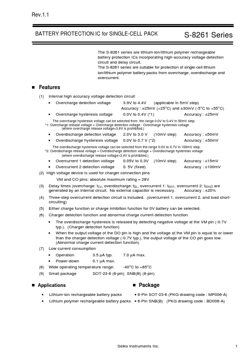
Symbol DO VM
CO DP VDD
Description
FET gate control pin for discharge (CMOS output)
Voltage detection pin between VM and VSS (Overcurrent detection pin)
FET gate control pin for charge (CMOS output)
Delay time
Symbol
Selection range
Overcharge detection delay time
tCU
0.15 s 1.2 s
Overdischarge detection delay time
tDL
36 ms 144 ms
Overcurrent 1 detection delay time
Seiko Instruments Inc.
3
BATTERY PROTECTION IC for SINGLE-CELL PACK S-8261 Series
Pin Assignment
Rev.1.1
6 54 SOT-23-6 Top view
高精度、高驱动电流、双运算放大器AD826说明书
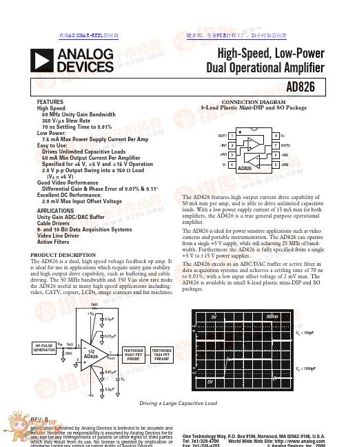
REV.BInformation furnished by Analog Devices is believed to be accurate and reliable. However, no responsibility is assumed by Analog Devices for its use, nor for any infringements of patents or other rights of third parties which may result from its use. No license is granted by implication oraAD826One Technology Way, P.O. Box 9106, Norwood, MA 02062-9106, U.S.A.Tel: 781/329-4700World Wide Web Site: High-Speed, Low-Power Dual Operational AmplifierCONNECTION DIAGRAM8-Lead Plastic Mini-DIP and SO Package12348765AD826V+OUT2–IN2+IN2OUT1–IN1+IN1V–The AD826 features high output current drive capability of 50mA min per amp, and is able to drive unlimited capacitive loads. With a low power supply current of 15 mA max for both amplifiers, the AD826 is a true general purpose operational amplifier.The AD826 is ideal for power sensitive applications such as video cameras and portable instrumentation. The AD826 can operate from a single +5 V supply, while still achieving 25 MHz of band-width. Furthermore the AD826 is fully specified from a single +5 V to ±15 V power supplies.The AD826 excels as an ADC/DAC buffer or active filter in data acquisition systems and achieves a settling time of 70 ns to 0.01%, with a low input offset voltage of 2 mV max. The AD826 is available in small 8-lead plastic mini-DIP and SO packages.10901000%500ns5V5VC L = 100pFC L = 1000pFFEATURES High Speed:50 MHz Unity Gain Bandwidth 350 V/s Slew Rate70 ns Settling Time to 0.01%Low Power:7.5 mA Max Power Supply Current Per Amp Easy to Use:Drives Unlimited Capacitive Loads50 mA Min Output Current Per AmplifierSpecified for +5 V, ؎5 V and ؎15 V Operation 2.0 V p-p Output Swing into a 150 ⍀ Load (V S = +5 V)Good Video PerformanceDifferential Gain & Phase Error of 0.07% & 0.11؇Excellent DC Performance:2.0 mV Max Input Offset Voltage APPLICATIONSUnity Gain ADC/DAC Buffer Cable Drivers8- and 10-Bit Data Acquisition Systems Video Line Driver Active FiltersPRODUCT DESCRIPTIONThe AD826 is a dual, high speed voltage feedback op amp. It is ideal for use in applications which require unity gain stability and high output drive capability, such as buffering and cable driving. The 50 MHz bandwidth and 350 V/µs slew rate make the AD826 useful in many high speed applications including:video, CATV, copiers, LCDs, image scanners and fax machines.TEKTRONIX P6201 FET PROBE HP PULSE GENERATOR1/2AD8261k ⍀50⍀1k ⍀C LV OUTV INTEKTRONIX 7A24 FET PREAMP؉V S0.01F3.3F0.01F–V S3.3F132Driving a Large Capacitive Load查询AD826AR-REEL供应商捷多邦,专业PCB打样工厂,24小时加急出货AD826–SPECIFICATIONS(@ T A = +25؇C, unless otherwise noted)Parameter Conditions V S Min Typ Max Unit DYNAMIC PERFORMANCEUnity Gain Bandwidth±5 V3035MHz±15 V4550MHz0, +5 V2529MHz Bandwidth for 0.1 dB Flatness Gain = +1±5 V1020MHz±15 V2555MHz0, +5 V1020MHz Full Power Bandwidth1V OUT = 5 V p-pR LOAD = 500 Ω±5 V15.9MHzV OUT = 20 V p-pR LOAD = 1 kΩ±15 V 5.6MHz Slew Rate R LOAD = 1 kΩ±5 V200250V/µsGain = –1±15 V300350V/µs0, +5 V150200V/µs Settling Time to 0.1%–2.5 V to +2.5 V±5 V45ns0 V–10 V Step, A V = –1±15 V45nsto 0.01%–2.5 V to +2.5 V±5 V70ns0 V–10 V Step, A V = –1±15 V70ns NOISE/HARMONIC PERFORMANCETotal Harmonic Distortion F C = 1 MHz±15 V–78dB Input Voltage Noise f = 10 kHz±5 V, ±15 V15nV/√Hz Input Current Noise f = 10 kHz±5 V, ±15 V 1.5pA/√Hz Differential Gain Error NTSC±15 V0.070.1% (R1 = 150 Ω)Gain = +2±5 V0.120.15%0, +5 V0.15% Differential Phase Error NTSC±15 V0.110.15Degrees (R1 = 150 Ω)Gain = +2±5 V0.120.15Degrees0, +5 V0.15Degrees DC PERFORMANCEInput Offset Voltage±5 V to ±15 V0.52mVT MIN to T MAX3mV Offset Drift10µV/°C Input Bias Current±5 V, ±15 V 3.3 6.6µAT MIN10µAT MAX 4.4µA Input Offset Current±5 V, ±15 V25300nAT MIN to T MAX500nA Offset Current Drift0.3nA/°C Open-Loop Gain V OUT = ±2.5 V±5 VR LOAD = 500 Ω24V/mVT MIN to T MAX 1.5V/mVR LOAD = 150 Ω 1.53V/mVV OUT = ±10 V±15 VR LOAD = 1 kΩ 3.56V/mVT MIN to T MAX25V/mVV OUT = ±7.5 V±15 VR LOAD = 150 Ω (50 mA Output)24V/mV INPUT CHARACTERISTICSInput Resistance300kΩInput Capacitance 1.5pF Input Common-Mode Voltage Range±5 V+3.8+4.3V–2.7–3.4V±15 V+13+14.3V–12–13.4V0, +5 V+3.8+4.3V+1.2+0.9V Common-Mode Rejection Ratio V CM = ±2.5 V, T MIN–T MAX±5 V80100dBV CM = ±12 V±15 V86120dBT MIN to T MAX±15 V80100dBAD826 ABSOLUTE MAXIMUM RATINGS1Supply Voltage . . . . . . . . . . . . . . . . . . . . . . . . . . . . . . .±18 VInternal Power Dissipation2Plastic (N) . . . . . . . . . . . . . . . . . . . . . See Derating CurvesSmall Outline (R) . . . . . . . . . . . . . . . . See Derating CurvesInput Voltage (Common Mode) . . . . . . . . . . . . . . . . . . .±V SDifferential Input Voltage . . . . . . . . . . . . . . . . . . . . . . .±6 VOutput Short Circuit Duration . . . . . . . See Derating Curves Storage Temperature Range (N, R) . . . . . . . –65°C to +125°C Operating Temperature Range . . . . . . . . . . –40°C to +85°C Lead Temperature Range (Soldering 10 seconds) . . . +300°C NOTES1Stresses above those listed under Absolute Maximum Ratings may cause perma-nent damage to the device. This is a stress rating only; functional operation of the device at these or any other conditions above those indicated in the operational section of this specification is not implied. Exposure to absolute maximum rating conditions for extended periods may affect device reliability .2Specification is for device in free air: 8-lead plastic package, θJA= 100°C/watt; 8-lead SOIC package, θJA = 155°C/watt.ORDERING GUIDETemperature Package Package Model Range Description Option AD826AN–40°C to +85°C8-Lead Plastic DIP N-8AD826AR–40°C to +85°C8-Lead Plastic SOIC SO-8 AD826AR-REEL7–40°C to +85°C7” Tape & Reel SOIC SO-8Parameter Conditions V S Min Typ Max Unit OUTPUT CHARACTERISTICSOutput Voltage Swing R LOAD = 500 Ω±5 V 3.3 3.8±VR LOAD = 150 Ω±5 V 3.2 3.6±VR LOAD = 1 kΩ±15 V13.313.7±VR LOAD = 500 Ω±15 V12.813.4±VR LOAD = 500 Ω0, +5 V+1.5,+3.5V Output Current±15 V50mA±5 V50mA0, +5 V30mA Short-Circuit Current±15 V90mA Output Resistance Open Loop8ΩMATCHING CHARACTERISTICSDynamicCrosstalk f = 5 MHz±15 V–80dB Gain Flatness Match G = +1, f = 40 MHz±15 V0.2dB Slew Rate Match G = –1±15 V10V/µs DCInput Offset Voltage Match T MIN–T MAX±5 V to ±15 V0.52mV Input Bias Current Match T MIN–T MAX±5 V to ±15 V0.060.8µA Open-Loop Gain Match V O = ±10 V, R LOAD = 1 kΩ,T MIN–T MAX±15 V0.150.01mV/V Common-Mode Rejection Ratio Match V CM = ±12 V, T MIN–T MAX±15 V80100dB Power Supply Rejection Ratio Match±5 V to ±15 V, T MIN–T MAX80100dB POWER SUPPLYOperating Range Dual Supply±2.5±18VSingle Supply+5+36V Quiescent Current/Amplifier±5 V 6.67.5mAT MIN to T MAX±5 V7.5mA±15 V7.5mAT MIN to T MAX±15 V 6.87.5mA Power Supply Rejection Ratio V S = ±5 V to ±15 V, T MIN to T MAX7586dB NOTES1Full power bandwidth = slew rate/2π VPEAK. Specifications subject to change without notice.ESD SUSCEPTIBILITYESD (electrostatic discharge) sensitive device. Electrostatic charges as high as 4000 volts, which readily accumulate on the human body and on test equipment, can discharge without detection. Although the AD826 features proprietary ESD protection cir-cuitry, permanent damage may still occur on these devicesif they are subjected to high energy electrostatic discharges. Therefore, proper ESD precautions are recommended to avoid any performance degradation or loss of functionality.2.0–50901.50.5–301.050703010–1080–40406020–20AMBIENT TEMPERATURE –؇CMAXIMUMPOWERDISSIPATION–WattsMaximum Power Dissipation vs. Temperature for Different Package TypesAD8262000201555101015I N P U T C O M M O N -M O D E R A N G E – ؎V o l t sSUPPLY VOLTAGE – ؎Volts–V CM+V CMFigure mon-Mode Voltage Range vs. Supply2000201555101015SUPPLY VOLTAGE – ؎VoltsO U T P U T V O L T A G E S W I N G – ؎V o l tsFigure 2.Output Voltage Swing vs. Supply 30010k1551001010201k25LOAD RESISTANCE – ⍀O U T P U T V O L T A G E S W I N G – V o l t s p -pFigure 3.Output Voltage Swing vs. Load Resistance7.75.70207.26.256.71015SUPPLY VOLTAGE – ؎VoltsQ U I E S C E N T S U P P L Y C U R R E N T P E R A M P – m AFigure 4.Quiescent Supply Current per Amp vs. Supply Voltage for Various TemperaturesS L E W R A T E – V /s20501510SUPPLY VOLTAGE– ؎Volts200300350400250Figure 5.Slew Rate vs. Supply Voltage10010.011k10k100M10M1M100k0.110FREQUENCY – HzC L O S ED -L O O P O U T P U T I M PE D A N C E – ⍀Figure 6.Closed-Loop Output Impedance vs. Frequency– Typical CharacteristicsAD8267114042–403–6065120806040100200–20TEMPERATURE – ؇CI N P U T B I A S C U R R E N T – AFigure 7.Input Bias Current vs. Temperature130301409050–4070–60110120100806040200–20TEMPERATURE – ؇CS H O R T C I R C U I T C U R R E N T – m AFigure 8.Short Circuit Current vs. Temperature 10020–601408040–4060100120806040200–20TEMPERATURE – ؇CP H A S E M A R G I N – D e g r e e s20804060U N I T Y G A I N B A N D W I D T H – M HzFigure 9.Unity Gain Bandwidth and Phase Margin vs. Temperature100–201G4010k201k 8060100M 10M1M 100k FREQUENCY – Hz+100+40+20+80+60P H A S E M A R G I N – D e g r e e sO P E N -L O O P G A I N – d BFigure 10.Open-Loop Gain and Phase Margin vs. Frequency411001k10k2356LOAD RESISTANCE – ⍀O P E N -L OO P G A I N – V /m V7Figure 11.Open-Loop Gain vs. Load Resistance10010100M30201k 10040506070809010M 1M 100k10k FREQUENCY – HzP S R – d BFigure 12.Power Supply Rejection vs. FrequencyAD826140601k 10M1208010k 100100k 1M FREQUENCY – HzC M R – dBFigure mon-Mode Rejection vs. Frequency 30100100k1M 100M10M 20FREQUENCY – HzO U T P U T V O L T A G E – V o l t s p -pFigure rge Signal Frequency Response 10–10160–4–820–602–20468140120100806040SETTLING TIME – ns O U T P U T S W I N G F R O M 0 T O ؎V0.01%0.1%1%1%0.01%0.1%Figure 15.Output Swing and Error vs. Settling Time –40–10010M–70–901k –80100–50–601M 100k 10k FREQUENCY – HzH A R M O N I C D I S T O R T I O N – dBFigure 16. Harmonic Distortion vs. Frequency50010M301010203401M100k 10k 1k 100FREQUENCY – HzI N P U T V O L T A G E N O I S E – nV / H zFigure 17. Input Voltage Noise Spectral Density380300–60140360320–40340100120806040200–20TEMPERATURE – ؇CS L E WR A T E – V /sFigure 18. Slew Rate vs. TemperatureAD826FREQUENCY – HzG A I N – d B50–5100k1M100M10M–1–2–3–41234Figure 19. Closed-Loop Gain vs. Frequency SUPPLY VOLTAGE – Volts0.130.070.10D I F FE R E N T IA L P H A S E – D e g r e e sD I F FE R E N T I A L G A I N – P e r c e n t0.10؎150.130.110.12؎5؎10Figure 20. Differential Gain and Phase vs. Supply Voltage –30–70–110100k100M10M1M10k–90–50–60–80–100–40FREQUENCY – HzC R O S S T A L K – d BFigure 21. Crosstalk vs. Frequency FREQUENCY – HZ50–5100k1M 100M10M –1–2–3–41234G A I N – dBFigure 22. Closed-Loop Gain vs. Frequency, Gain = –1FREQUENCY – HzG A I N – d B1.00–1.0100k1M 100M10M –0.2–0.4–0.6–0.80.20.40.60.8Figure 23. Gain Flatness Matching vs. Supply, G = +1USE GROUND PLANEPINOUT SHOWN IS FOR MINIDIP PACKAGEV R L = 150⍀ FOR ؎V S = 5V, 1k ⍀ FOR ؎V S = 15VFigure 24. Crosstalk Test CircuitAD826Figure 25. Noninverting Amplifier ConfigurationFigure 26. Noninverting Large Signal Pulse Response, R L = 1 k ΩFigure 27. Noninverting Large Signal Pulse Response,R L = 150ΩFigure 28. Noninverting Small Signal Pulse Response, R L = 1 k ΩFigure 29.Noninverting Small Signal Pulse Response, R L = 150 ΩAD826Figure 30.Inverting Amplifier ConfigurationFigure 31.Inverting Large Signal Pulse Response,R L = 1 kΩFigure 32.Inverting Large Signal Pulse Response,R L = 150ΩFigure 33.Inverting Small Signal Pulse Response,R L = 1 kΩFigure 34.Inverting Small Signal Pulse Response,R L = 150 ΩAD826THEORY OF OPERATIONThe AD826 is a low cost, wide band, high performance dual operational amplifier which can drive heavy capacitive and resistive loads. It also achieves a constant slew rate, bandwidth and settling time over its entire specified temperature range. The AD826 (Figure 35) consists of a degenerated NPN differen-tial pair driving matched PNPs in a folded-cascode gain stage. The output buffer stage employs emitter followers in a class AB amplifier which delivers the necessary current to the load while maintaining low levels of distortion.–INNULL 1NULL 8S–VSFigure 35. Simplified SchematicThe capacitor, C F, in the output stage mitigates the effect of capacitive loads. With low capacitive loads, the gain from the compensation node to the output is very close to unity. In this case, C F is bootstrapped and does not contribute to the overall compensation capacitance of the device. As the capacitive load is increased, a pole is formed with the output impedance of the output stage. This reduces the gain, and therefore, C F is incompletely bootstrapped. Effectively, some fraction of C F contributes to the overall compensation capacitance, reducing the unity gain bandwidth. As the load capacitance is further increased, the bandwidth continues to fall, maintaining the stability of the amplifier.INPUT CONSIDERATIONSAn input protection resistor (R IN in Figure 25) is required in circuits where the input to the AD826 will be subjected to transient or continuous overload voltages exceeding the ±6 V maximum differential limit. This resistor provides protection for the input transistors by limiting their maximum base current. For high performance circuits, it is recommended that a “bal-ancing” resistor be used to reduce the offset errors caused by bias current flowing through the input and feedback resistors. The balancing resistor equals the parallel combination of R IN and R F and thus provides a matched impedance at each input terminal. The offset voltage error will then be reduced by more than an order of magnitude.APPLYING THE AD826The AD826 is a breakthrough dual amp that delivers precision and speed at low cost with low power consumption. The AD826 offers excellent static and dynamic matching characteristics, combined with the ability to drive heavy resistive and capacitive loads.As with all high frequency circuits, care should be taken to main-tain overall device performance as well as their matching. The following items are presented as general design considerations. Circuit Board LayoutInput and output runs should be laid out so as to physically isolate them from remaining runs. In addition, the feedback resistor of each amplifier should be placed away from the feedback resistor of the other amplifier, since this greatly reduces inter-amp coupling.Choosing Feedback and Gain ResistorsIn order to prevent the stray capacitance present at each amplifier’s summing junction from limiting its performance, the feedback resistors should be ≤ 1 kΩ. Since the summing junction capaci-tance may cause peaking, a small capacitor (1 pF–5pF) may be paralleled with R F to neutralize this effect. Finally, sockets should be avoided, because of their tendency to increase interlead capacitance.Power Supply BypassingProper power supply decoupling is critical to preserve the integrity of high frequency signals. In carefully laid out designs, decoupling capacitors should be placed in close proximity to the supply pins, while their lead lengths should be kept to a mini-mum. These measures greatly reduce undesired inductive effects on the amplifier’s response.Though two 0.1µF capacitors will typically be effective in decoupling the supplies, several capacitors of different values can be paralleled to cover a wider frequency range.AD826؎SINGLE SUPPLY OPERATIONAn exciting feature of the AD826 is its ability to perform well in a single supply configuration (see Figure 37). The AD826 is ideally suited for applications that require low power dissipation and high output current and those which need to drive large capacitive loads, such as high speed buffering and instrumentation. Referring to Figure 36, careful consideration should be given to the proper selection of component values. The choices for this particular circuit are: (R1 + R3)ʈR2 combine with C1 to form a low frequency corner of approximately 30 Hz.OUT0.1VFigure 36. Single Supply Amplifier Configuration R3 and C2 reduce the effect of the power supply changes on the output by low-pass filtering with a corner at12πR3C2.The values for R L and C L were chosen to demonstrate the AD826’s exceptional output drive capability. In this configura-tion, the output is centered around 2.5 V. In order to eliminate the static dc current associated with this level, C3 was inserted in series with R L.Figure 37.Single Supply Pulse Response, G = +1,R L = 150Ω, C L = 200 pFPARALLEL AMPS PROVIDE 100 mA TO LOADBy taking advantage of the superior matching characteristics ofthe AD826, enhanced performance can easily be achieved byemploying the circuit in Figure 38. Here, two identical cells areparalleled to obtain even higher load driving capability than thatof a single amplifier (100 mA min guaranteed). R1 and R2 areincluded to limit current flow between amplifier outputs thatwould arise in the presence of any residual mismatch.LFigure 38.Parallel Amp ConfigurationAD826SINGLE-ENDED TO DIFFERENTIAL LINE DRIVEROutstanding CMRR (> 80 dB @ 5 MHz), high bandwidth, wide supply voltage range, and the ability to drive heavy loads, make the AD826 an ideal choice for many line driving applications.In this application, the AD830 high speed video difference amp serves as the differential line receiver on the end of a back terminated, 50 ft., twisted-pair transmission line (see Figure 40).The overall system is configured in a gain of +1 and has a –3 dB bandwidth of 14 MHz. Figure 39 is the pulse response with a 2 V p-p, 1 MHz signal input.Figure 39.Pulse ResponseFigure 40.Differential Line DriverLOW DISTORTION LINE DRIVERThe AD826 can quickly be turned into a powerful, low distor-tion line driver (see Figure 41). In this arrangement the AD826can comfortably drive a 75Ω back-terminated cable, with a 5MHz, 2 V p-p input; all of this while achieving the harmonic distortion performance outlined in the following table.Configuration 2nd Harmonic 1.No Load –78.5 dBm 2.150 Ω R L Only –63.8 dBm 3.150Ω R L 7.5Ω R C–70.4 dBmIn this application one half of the AD826 operates at a gain of 2.1 and supplies the current to the load, while the other pro-vides the overall system gain of 2. This is important for two reasons: the first is to keep the bandwidth of both amplifiers the same, and the second is to preserve the AD826’s ability to oper-ate from low supply voltages. R C varies with the load and must be chosen to satisfy the following equation:R C = MR Lwhere M is defined by [(M+ 1) G S = G D ] and G D = Driver ’s Gain,Figure 41.Low Distortion AmplifierAD826HIGH PERFORMANCE ADC BUFFERFigure 42 is a schematic of a 12-bit high speed analog-to-digital converter. The AD826 dual op amp takes a single ended input and drives the AD872 A/D converter differentially, thus reduc-ing 2nd harmonic distortion. Figure 43 is a FFT of a 1MHz input, sampled at 10 MHz with a THD of –78 dB. The AD826can be used to amplify low level signals so that the entire range of the converter is used. The ability of the AD826 to perform on a ±5 volt supply or even with a single 5 volts combined with its rapid settling time and ability to deliver high current to compli-cated loads make it a very good flash A/D converter buffer as well as a very useful general purpose building block.V Figure 42.A Differential Input Buffer for High Bandwidth ADCsFigure 43.FFT, Buffered A/D ConverterAD826OUTLINE DIMENSIONSDimensions shown in inches and (mm).8-Lead Plastic Mini-DIP (N) Package8-Lead SO (R) Package45؇All brand or product names mentioned are trademarks or registered trademarks of their respective holders.C 1807a –0–6/00 (r e v . B ) 00877P R I N T ED I N U .S .A .。
泰特8260双频移动无线电设备说明书
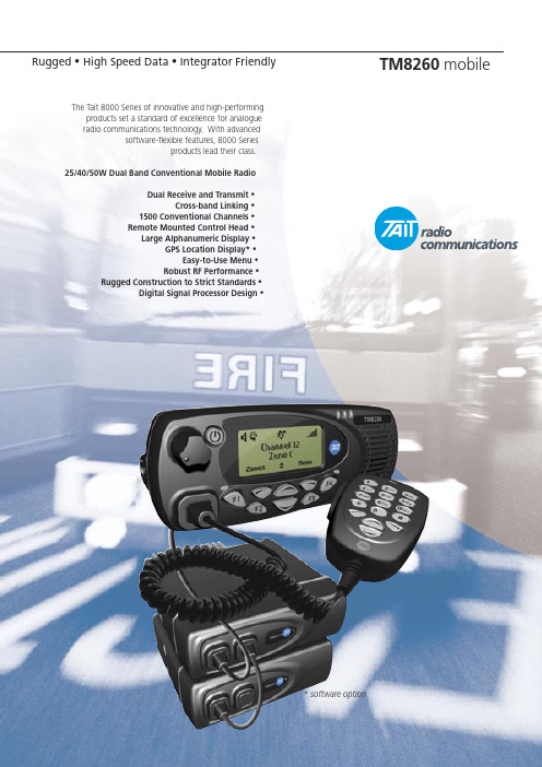
TM8260 mobile Rugged • High Speed Data • Integrator FriendlyThe Tait 8000 Series of innovative and high-performingproducts set a standard of excellence for analogueradio communications technology. With advancedsoftware-flexible features, 8000 Seriesproducts lead their class.25/40/50W Dual Band Conventional Mobile RadioDual Receive and Transmit •Cross-band Linking •1500 Conventional Channels •Remote Mounted Control Head •Large Alphanumeric Display •GPS Location Display* •Easy-to-Use Menu •Robust RF Performance •Rugged Construction to Strict Standards •Digital Signal Processor Design •* software optionThe TM8260 dual band radio system is ideal for public safety incident management where cost-effective interoperability between different groups of personnel is essential.The high performance TM8260 system provides a flexible solution for conventional radio communications in mission-critical situations. It features dual radio bodies offering an extended frequency range, controlled by a single control head.With features such as cross-band linking and the ability to receive and transmit simultaneously on two frequency bands, the TM8260 enables emergency services to have reliable and effective communications in any situation.This system not only assists in co-operation between different services, it enables supervisors to gain an overview and control of the front line and connectivity to control centres.Backed by more than 30 years of Tait experience, knowledge and support, the TM8260 is much more than just a radio. It is a cost-effective public safety solution designed to give the best return for your organisation.TM8260 mobileEasy to Read DisplayThe powerful TM8260 control head features a largealphanumeric display, providing clear information for users such as emergency response teams who rely on communications to stay in control of highly unpredictable situations.The easy-to-read display enables users to clearly and easily view channel information, including text, icons and even GPS location information. The services supported by the system are clearly indicated, such as cross-band linking and dual transmit. The TM8260 also features four function keys that can be programmed for fast one-touch access to commonly used features.Intuitive Menu StructureThis radio features a comprehensive user-friendly menu that allows easy navigation of all functions, including channel access, display settings, dual transmit and receive, and cross-band repeater mode.Dual Transmit and ReceiveIn a TM8260 system, two separate frequency bands can be monitored simultaneously with no manual switching needed. Users can also transmit to two separate groups of personnel at the same time, such as two emergency services working to-gether in an incident situation. In normal operation the system can also be programmed to work as a single radio.Cross Band LinkingThe TM8260 can operate as a cross-band repeater, where transmissions received on one radio can automatically be transmitted on the other. This would ensure reliablecommunication between a control centre and personnel at a fire scene, with no need to man and relay messages through the fire appliance.1500 Conventional ChannelsEach radio in a TM8260 dual band system supports 1500 conventional channels and 300 scanning and voting groups. This makes it an ideal communications solution where many radio frequencies are deployed to provide communication between different emergency services.Remote Mounted Control HeadThe control head for the TM8260 system is mounted separately to the two radio bodies, allowing more flexibility for vehicle installers particularly where space is limited. The remote control head can be mounted up to six metres away from the radio bodies.GPS Location Display (Optional)The TM8260 system can be connected to a GPS receiver, to im-prove safety and efficiency where independent groups of users are working together. When the radio is loaded with optional GPS software, location information such as latitude, longitude, course and speed can be viewed on the control head display. This may be supplemented by the display of map reference in various formats e.g. UTM, RTC.FeaturesRobust RF Performance, Rugged ConstructionThe TM8260 has been developed using innovative RF design and includes a number of features to maintain operation even under harsh conditions.The radio has been engineered with a strong diecast metal chassis and almost entirely constructed using Surface Mount Technology (SMT). It is IP54 rated and meets stringentspecifications for reliability including MIL-STD 810 C, D, E & F .Advanced System Integration CapabilitiesThis radio has been designed with customisation in mind. System integrators have maximum design flexibility with multiple ports for auxiliary connectors and a large options board area. A comprehensive range of development kits is supported, which provide hardware and software tools for customisation.Optional Features:Locking Security Cradle High Speed Data Modem GPS Location Display Power Supply••••TM8260 SpecificationsAuthorised Dealer* Please contact your nearest Tait office or authorised dealer for further frequency band combinations.B M 8260-0GeneralFrequency Range*VHF UHFStandard 136–174MHz 400–470MHz 450–530MHz High Power 136–174MHz 400–470MHz 450–520MHzFrequency Stability ±1.5ppmChannel/Network Capacity 1500 Conventional Channels 300 Scan/Vote Groups Power Supply 10.8–16VDC Channel Spacing 12.5/20/25kHz Channel Increment 7.5/12.5/15/25/30kHzDimensions (LxWxH)25W 40/50W 185 x 182 x 70mm (7.3 x 7.2 x 2.8in)205 x 182 x 70mm (8.1 x 7.2 x 2.8in)Weight 25W 40/50W1.5kg (53oz)1.7kg (59oz)Operational Temperature -30ºC to +60ºC (-22ºF to +140ºF)SealingPasses dust and rain testing to IP54RF Connector 25W 40/50W50 ohm BNC50 ohm BNC or Mini UHFInterface Connectors3 Interface Connectors with Serial Ports Military Standards 810 F**Applicable MIL-STDMethod Procedure Low PressureHigh Temperature Low Temperature Temperature Shock Solar Radiation RainHumidity Salt Fog DustVibration Shock500.4501.4502.4503.4505.4506.4507.4509.4510.4514.5516.521, 21, 2111, 311111, 5**also meets equivalent superseded MIL-STD 810 C, D & E.TransmitterOutput Power25W 40W 50WUHF VHF25W, 10W, 5W, 1W 40W, 20W, 15W, 10W 50W, 25W, 15W, 10WModulation Limiting 12.5kHz 20kHz 25kHz±2.5kHz ±4kHz ±5kHz FM Hum and Noise 12.5kHz 25kHz-38dB -43dBConducted/Radiated Emissions -36dBm <1GHz -30dBm >1GHz Audio Response 300Hz–3kHzFlat or pre-emphasisedAudio Distortion 3% at 1kHz 60% modulation (typical)Transmit Rise Time 10msDuty Cycle33% at 25W 20% at 40/50WReceiverSensitivity VHF/UHF<-118dBm for 12dB SINAD (0.28µV)Intermodulation 67dBSelectivity 12.5kHz 20kHz 25kHz65dB 70dB 75dB Spurious Responses 72dB Hum and Noise 12.5kHz 25kHz-40dB -43dBAudio Response 300Hz–3kHzFlat or de-emphasisedAudio Distortion3% at 1kHz 60% modulation (typical)Specifications are subject to change without notice and shall not form part of any contract. They are issued for guidance purposes only. Please note that not all frequency bands and power outputs are available in all markets. For further information please check with your nearest Tait office or authorised dealer.The word Tait and the Tait logo are trademarks of TaitElectronics Ltd. Tait is an ISO9001: 2000 and ISO14001: 2004 certified supplier.Regulatory DataFrequency FCC Description25W 136-174400-470450-530CASTMAB1C CASTMAH5C CASTMAH6C 40W 400-470450-520CASTMAH5D CASTMAH7D 50W136-174CASTMAB1D。
ICP DAS PIO-821LU HU 系列快速入门指南说明书

The package includes the following items:Step 1: Setup the Windows driver. The driver is located at:Check the Supplied ItemsInstalling Windows DriverThe PIO-821 series classic driver supports Windows 98/NT/2K and 32-bit XP/ 2003/ Vista/7/8. Recommended to install this driver for have been used PIO-821 series boards of regular user , please refer to :/pub/cd/iocard/pci/napdos/pci/pio-821/manual/quickstart /classic/Step 2: Click the “Next>” button to start the installation.Step 3: Check your DAQ Card is or not on supported list, then click the“Next>” button.Step 4: Select the installed folder, the default path is C:\ICPDAS\UniDAQ ,confirm and click the “Next>” button.Step 5: Check your DAQ Card on list, then click the “Next>” button. Step 6: Click the “Next>” button on the Select Additional Tasks window. Step 7: Click the “Next>” button on the Download Information window. Step 8: Select “No, I will restart my computer later ” and then click the“Finish ” button.For detailed information about the driver installation, please refer to Chapter 2.1 “Getting the UniDAQ Driver DLL Installer package ” of the UniDAQ SDK user manual.Jumper Setting12 3567Please make sure JP4 jumper is kept in default setting before self-test, asSetting Reference: For more detailed jumper information, please refer to manual section 2.3 and 2.4. (CD:\NAPDOS\PCI\PIO-821\manual\)Step 1: Shut down and power off your computer. Step 2: Remove the cover from the computer. Step 3: Select an unused PCI slot.Step 4: Carefully insert your I/O card into the PCI slot. Step 5: Replace the PC cover.Step 6: Power on the computer.After powering-on the computer, please finish the Plug&Play steps according to the prompted messages.Installing Hardware on PCPin Assignments⏹CON1/CON2 Digital Input/Output Connector (20-pin box header)⏹CON3 AD, DA and Timer/Counter Connector (Female DB37)⏹ DIO Test Wiring:1. Use CA-2002 (optional) cable to connect the CON1 with CON2.⏹ Analog Input Test Wiring:2. Prepare for device:● DN-37 (optional) Wiring terminal board.● Provide a stable signal source. (For example, dry battery)3. Connect the DN-37 to the CON3 on the board using the CA-3710 (optional) cable.Self-TestCA-2002CON34. Wire the signal source to channel 0, and then keep set the JP4 jumper to Single-Ended (page 3), and wire the signals as follows:Connect the AI 0 (Pin01) to signal positive (+) Connect the A.GND (Pin09) to signal negative (-)5. Execute the UniDAQ Utility Program.This program (UniDAQ Utility) will be placed in the default path after completing installation. The UniDAQ Utility.exe is located in (Default path): C:\ICPDAS\UniDAQ\Driver\Double-Click 16. Get DIO function test result.Select the “Port 0”8The corresponding D/I becomes red for channel 0, 2, 4, 6 of D/O is ON.9Select the “Port 0”.Check channel 0, 2, 4, 6657. Get A/D function test result.⏹PIO-821LU/HU Series Card Product Page:/root/product/solutions/pc_based_io_board/pci/pio-821.html⏹DN-37, CA-3710 and CA-2002 page (optional):/products/DAQ/screw_terminal/dn_37.htm/products/Accessories/cable/cable_selection.htm ⏹Documentation and Software: CD:\NAPDOS\PCI\UniDAQ\/pub/cd/iocard/pci/napdos/pci/unidaq/Related InformationCheck analog input on Channel 0 textbox. The other channels value for floating number .13。
CH9121网络和UART透明传输芯片说明书
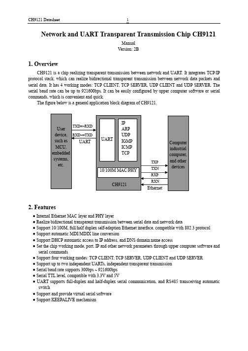
Network and UART Transparent Transmission Chip CH9121ManualVersion: 2B1.OverviewCH9121 is a chip realizing transparent transmission between network and UART. It integrates TCP/IP protocol stack, which can realize bidirectional transparent transmission between network data packets and serial data. It has 4 working modes: TCP CLIENT, TCP SERVER, UDP CLIENT and UDP SERVER. The serial baud rate can be up to 921600bps. It can be easily configured by upper computer software or serial commands, which is convenient and quick.The figure below is a general application block diagram of CH9121.2.Features●Internal Ethernet MAC layer and PHY layer●Realize bidirectional transparent transmission between serial data and network data●Support 10/100M, full/half duplex self-adaption Ethernet interface, compatible with 802.3 protocol●Support automatic MDI/MDIX line conversion●Support DHCP automatic access to IP address, and DNS domain name access●Set the chip working mode, port, IP and other network parameters through upper computer software andserial commands●Support four working modes: TCP CLIENT, TCP SERVER, UDP CLIENT and UDP SERVER●Support up to two independent UARTs, independent transparent transmission●Serial baud rate supports 300bps ~ 921600bps●Serial TTL level, compatible with 3.3V and 5V●UART supports full-duplex and half-duplex serial communication, and RS485 transceiving automaticswitch●Support and provide virtual serial software●Support KEEPALIVE mechanism3.PackageChipPackageName DescriptionCH9121 LQFP64M LQFP package; 64 pins; package body 10 x10mm 4.PinsCH9121 Pin No.PinNamePin Type Pin description2, 12, 17, 21, 29, 40, 42, 45, 63 VCC33 Power3.3V positive power input, require an external 0.1uF powerdecoupling capacitor6, 19, 28, 43, 54, 64 VCC18 Power1.8V positive power input, require an external 0.1uF powerdecoupling capacitor3, 9, 13, 18, 20,37, 41, 44, 48GND Power Common ground14, 15, 16, 22,23, 24, 25, 26,27, 34, 35, 38,39, 47, 49, 50,61, 62NC - Reserved, suspended1 RSETE Input Connected with an external 18K resistor to ground4 RXP EthernetsignalEthernet RXP signal5 RXN Ethernet Ethernet RXN signalsignal7 TXP EthernetsignalEthernet TXP signal8 TXN EthernetsignalEthernet TXN signal10 XI Input Input of the crystal oscillator, requires an external 30MHzcrystal11 XO Output Inverted output of crystal oscillator, requires an external 30MHzcrystal30 TCPCS1 Output In TCP client mode, connection status indicator of port 1, activeat low level31 RUN Output CH9121 running status indicator pin, multiplexed as ISPupgrade pin32 CFGEN Input Network configuration enable pin, detects when power-up, configuration disabled when at low level33 TCPCS2 Output In TCP client mode, connection status indicator of port 2, activeat low level36 RSTI Input External reset input, active at low level, built-in pull-up resistor 46 DIR2 Output Used to control RS485 receiving/transmitting switch of UART251 DIR1 Output Used to control RS485 receiving/transmitting switch of UART152 ACT# Output Ethernet connection communication indicator LED drive pin53 LINK# Output PHY connection indicator LED, active low55 RXD2 Input Serial data input of UART2, built-in pull-up resistor(Off by default)56 TXD2 Output Serial data output of UART2 (Off by default)57 RXD1 Input Serial data input of UART1, built-in pull-up resistor(On by default)58 TXD1 Output Serial data output of UART1 (On by default)59 RESET InputRestore factory settings, chip power-on detection, active at low level60 CFG0 InputUART configuration mode set pin, built in pull-up. If low level is detected, enter UART configuration mode. Exit the mode if high level is detected5.Function5.1. Function DescriptionCH9121 is a chip for transparent transmission between network and UART, and realizes bidirectional transparent transmission of serial data and network data. It supports 4 working modes (TCP CLEINT/SERVER, UDP CLIENT/SERVER), and the serial baud rate supported ranges from 300bps to 921600bps. Before use, the network parameters and UART parameters of the chip shall be configured by upper computer software NetModuleConfig.exe or serial commands. After the configuration is completed, CH9121 will save the configuration parameters to the internal storage space. And after the chip is reset, CH9121 will work according to the saved configuration value.The basic parameters of CH9121 include: name, MAC address display, dynamic access IP address setting, manual IP address setting (including CH9121 IP address, subnet mask, default gateway), and UART negotiation configuration.The name is mainly for the convenience of CH9121 module management within the LAN, with the length of not more than 20 bytes. The MAC address field shows the MAC address of the currently selectedmodule. There are two ways for CH9121 to set network parameters. 1) DHCP, that is, it automatically obtains network parameters from the gateway device with DHCP SERVER function; 2) manual setting. UART negotiation configuration function is to enter serial configuration mode by handshaking through the UART, which is disabled by default.CH9121 port parameters include: network mode, local port, target IP/domain name, destination port, serial baud rate/data bit/stop bit/parity check bit, network cable disconnection processing, RX packet length, RX packet timeout interval, network connection operation.The network mode (TCP SERVER/CLIENT, UDP SERVER/CLIENT), destination IP address, and local/destination port are the basic parameters of network communication. The destination IP address can also be accessed by domain name. The serial baud rate ranges from 300bps to 921600bps (the baud rate error of the serial port transmitting signal is less than 0.3%, and the allowable baud rate error of the serial port receiving signal is not less than 2%). It supports 5/6/7/8 data bits, 1/2 stop bits, odd/even/no parity check, blank 0, and mark 1 check mode. The network cable disconnection processing means that when the network cable is disconnected, CH9121 actively closes the connection or does not take any action. The length range of RX packet is 1-1024, which means that when the length of CH9121 UART receiving data reaches the set length, CH9121 will immediately packet the serial data and send it out via network. The timeout time setting range is 0-200, and the timeout unit is about 5ms. For example, when the timeout is 1, the data length of the serial port receiving buffer does not reach the length of the RX packet, and the serial port does not receive a new one in more than 5ms, the serial port timeout will occur. After the serial port timeout occurs, CH9121 will send the data received by the serial port over the network. When the timeout time is set to 0, the internal hardware timeout mechanism will be enabled (no new data is received after 4 data times), which is suitable for occasions where real-time requirements are high and large quantities of data are sent and received. Clear serial port buffer setting refers to how the data received by the serial port is processed before the network connection is established, the data is cleared (discarded) or retained after TCP connection.5.2. Default ConfigurationWhen CH9121 leaves factory, port 2 is closed and port 1 works in TCP CLIENT mode by default. The default parameters related to the network are as follows:(1)Device IP: 192.168.1.200(2)Subnet mask: 255.255.255.0(3)Default gateway: 192.168.1.1(4)Module port: 2000(5)Destination IP: 192.168.1.100(6)Destination port: 1000(7)Number of reconnection: unlimitedUART related default parameters are:(1)Baud rate: 9600(2)Timeout: 0(3)Data bit: 8. Stop bit: 1. Parity check bit: No(4)Clear UART buffer: Never6.Parameters6.1. Absolute Maximum ValueCritical value or exceeding the absolute maximum value may cause the chip to work abnormally or even be damaged.Name Parameter description Min. Max. UnitTA Ambient temperature during operation VCC33=3.3VVCC18=1.8V-40 85 ℃TS Ambient temperature during storage -55 125 ℃VCC33 Supply voltage (VCC33 connects to power, GND to ground) -0.4 4.2 V VCC18 Supply voltage (VCC18 connects to power, GND to ground) -0.4 2.3 V VIO Voltage on input or output pins -0.4 VCC33+0.4 V VIO5 Voltage on input or output pins that support 5V withstand voltage -0.4 5.4 V6.2. Electrical ParametersTest Conditions: TA=25℃, VCC33=3.3V, VCC18=1.8VName Parameter description Min. Typ. Max. UnitVCCxx Supply voltage VCC33 2.7 3.3 3.6V VCC18 1.65 1.8 1.95ICC Total supply current duringoperationVCC33=3.3V 160 190 mAVIL Low level input voltage -0.4 0.7 V VIH High level input voltage 2.0 VCC33+0.4 V VOL Low level output voltage (4mA draw current) 0.4 V VOH High level output voltage (4mA output current) VCC33-0.4 VIUP Input current at the input terminal with built-inpull-up resistor20 40 100 uAIDN Input current at the input terminal with built-inpull-down resistor-20 -40 -100 uAVR Voltage threshold when power-on reset 1.4 1.5 2.5 V7.Applications7.1 Hardware Circuit DesignNote: Due to space limitations, the circuit of the power supply and decoupling capacitors near the 3.3V and 1.8V pins is omitted in the figure, which must be added when designing the circuit. The detailed circuit reference file: CH9121PCB (please download in our official website).U1 is the main control chip CH9121. TXD1 and RXD1 are compatible with 3.3V and 5V level, and the RS485 control pin DIR can be suspended if not used.P1 is RJ45 port, with built-in network transformer, used to connect network equipments such as switches and router. It contains two pairs of Ethernet differential signals.When actually making a PCB, R5-R8, C6, and C7 should be as close as possible to the 5th pin of P1. The 0.1 uF decoupling capacitors for 3.3V and 1.8V pins are omitted in the figure. TXOP (RXIP) and TXON. (RXIN) are differential signals. When wiring, they should be wired close to parallel, and try to provide ground wire or copper coating on both sides to reduce external interference. The length of relevant signals of crystals XI and XO should be shortened as much as possible. In order to reduce the interference of high-frequency clock for the outside, the baselines should be surrounded or copper should be clad around relevant components.。
gdm8261a使用手册
gdm8261a使用手册一、产品简介GDM8261a是一款高性能的设备,广泛应用于各种行业。
本产品具备出色的性能和稳定性的特点,为用户带来高效的工作体验。
在此,我们为您提供详细的使用手册,帮助您更好地了解和掌握产品的功能和使用方法。
二、产品特点1.高性能:GDM8261a采用先进的技术,具有较高的处理速度和数据传输速率,满足用户对高效工作的需求。
2.稳定性:本产品在设计过程中充分考虑了各种因素,确保设备在长时间运行过程中保持稳定性能。
3.易于操作:GDM8261a的操作界面简洁直观,让用户可以轻松上手,快速掌握使用方法。
4.多功能:本产品具备丰富的功能,可以满足不同行业的需求。
三、使用方法1.开机:将电源线插入电源插座,然后按下设备开关,开机成功后,设备会自动进入工作状态。
2.设置:根据实际需求,通过操作界面进行相关设置,如速度、温度等。
3.操作:在确认设置无误后,启动设备,进行相关操作。
4.关机:完成工作后,按下设备关机键,待设备完全停止后,拔掉电源线。
四、注意事项1.请勿在设备运行时触摸或移动,以免造成人身伤害。
2.保持设备清洁,定期清理灰尘,以免影响设备性能。
3.使用过程中,如发现异常声音、异味等情况,请立即停止使用,并联系售后服务。
4.不要在潮湿、高温、通风不良的环境中使用设备,以免影响使用寿命。
五、故障处理1.若设备无法开机,请检查电源线是否连接正常,电源插座是否正常供电。
2.若设备运行中突然停止,请检查电源线是否松动,或者设备是否过载。
3.若显示异常,请检查连接线是否正常,显示器是否损坏。
六、售后服务本公司为您提供完善的售后服务,如在使用过程中遇到任何问题,请随时联系我们。
我们将竭诚为您解答和处理。
通过以上介绍,相信您已经对GDM8261a有了更深入的了解。
gdm8261a使用手册

gdm8261a使用手册摘要:一、前言二、产品概述三、安装与设置1.准备工作2.安装步骤3.设置与配置四、功能与操作1.主界面与功能模块2.参数设置与调整3.数据记录与分析五、维护与故障排除1.日常维护2.故障排查方法3.常见故障与解决办法六、产品升级与售后服务1.产品升级2.售后服务七、结语正文:【前言】gdm8261a 使用手册为您提供了详细的安装、使用和维护指导。
本手册旨在帮助您更好地了解和操作gdm8261a 产品,充分发挥其性能优势,为您的日常工作和生活带来便利。
【产品概述】gdm8261a 是一款功能强大、易于使用的设备。
它具有稳定的性能、紧凑的设计和丰富的接口,适用于多种应用场景。
本章将介绍gdm8261a 的产品特点、适用范围及相关技术参数。
【安装与设置】为了确保gdm8261a 的正常运行,安装和设置至关重要。
本章将详细介绍安装前的准备工作、安装步骤以及如何进行设置和配置。
【功能与操作】本章将详细介绍gdm8261a 的功能模块、主界面以及参数设置与调整方法。
同时,您将了解到如何进行数据记录与分析,以便更好地使用gdm8261a。
【维护与故障排除】为了确保gdm8261a 的稳定运行,本章将介绍日常维护的方法和注意事项。
此外,还将介绍故障排查的方法和步骤,以及常见故障的解决办法,帮助您快速解决实际问题。
【产品升级与售后服务】本章将介绍如何进行产品升级,以保持gdm8261a 的性能优势。
同时,将为您提供售后服务渠道和联系方式,确保您在使用过程中能够得到及时的支持和帮助。
【结语】通过本使用手册,相信您已经对gdm8261a 有了更深入的了解。
希望本手册能够帮助您更好地使用gdm8261a,为您的日常工作和生活带来便利。
如果您在使用过程中遇到任何问题,请随时与我们的售后服务团队联系。
DIM-826 使用手册说明书

Version 2PUB. DIM-8262Corel Application Disc - Movie Backup, Playback, Editing and TransferThe Corel Application Disc CD-ROM includes software that will allow you to back up or play back movies, transfer movies to a computer and easily edit them, and more. For further details, refer to the help files of each program.GuideMenu - Movie Backup and Transfer7)•Save backup copies of your video recordings on a computer.•Transfer movies from the computer back to the camcorder and play them back with the camcorder.DVD MovieFactory SE - Video Editing and DVDAuthoring 10)•Touch up your videos by cutting, deleting and moving scenes.•Add music, titles and transition effects.•Create your own personalized DVD menus.Start the program by selecting [Authoring] in the GuideMenu screen. For further details, refer to therelevant sections in this manual and the help files of the program.WinDVD SE - Movie Playback 13)•Play back your discs, either standard-definition DVD discs or high-definition AVCHD discs.•Play back video files saved on the computer using GuideMenu.For further details, refer to the help files of the program.For support concerning Corel Application DiscPlease call one of the customer support centers or access the support services online (details on the back cover). Canon-related customer support centers cannot provide support regarding software in the Corel Application Disc CD-ROM.3System RequirementsSystem requirements will vary based on the applications and features you choose to install. The applications may not work correctly depending on the specifications and settings of your computer and the software already installed.Make sure you have a valid Internet connection. You will not be able to use the software without successfully completing the user registration.1Recommended System Configuration* for Corel Application Disc Minimum Configuration* Required for the “Save Files to PC”, “Write Back to Camcorder” Options (GuideMenu)* Equivalent or better configurations can be used instead.**The available hard disk space required will vary depending on the amount of data being backed up.Operating SystemMicrosoft Windows XP SP2Microsoft Windows VistaCPU Intel Core 2 Duo 1.86 GHz / Intel Pentium D 3.2 GHzRAM1 GB2 GBAvailable Hard Disk SpaceInstallation only: At least 1 GBDisc authoring: At least twice the amount of data to be recorded on the disc(for a full standard-size (12 cm) DVD-R/DVD-RW - at least 10 GB)Graphic Accelerator NVIDIA GeForce 6600, 128 MB / ATI Radeon X700 Series, 128 MBMonitor/Display 1024 x 768 color display with 16-bit color video cardOthersDVD drive with writing capabilities compatible with DVD-R/DVD-RW discs,Internet connection (required for user registration)Operating System Microsoft Windows XP SP2Microsoft Windows Vista CPU Intel Pentium 4, 1.6 GHzIntel Pentium 4, 2.4 GHzRAM512 MB1 GBAvailable Hard Disk Space At least 3 GB(“Save Files to PC” only)**OthersDVD drive with writing capabilities compatible withDVD-R/DVD-RW discs4Software InstallationTurn on the computer and start Windows. Check that the camcorder is not connected to the computer.1Insert the Corel Application DiscCD-ROM into the computer’s CD or DVD drive.The InstallShield Wizard will launch automatically.2Select the language for theinstallation from the drop-down menu and click [OK].3Click [Next].Read the license agreement andclick [Next].Select [I accept the terms of thelicense agreement] to continue.Enter the user information andclick [Next].Enter your name and (optionally) your company affiliation.Check the destination folder forthe installation files and click [Next].Select your country/region ofresidence or the local video standard and click [Next].Review the installation settingsand click [Next] to start copying the files.25User RegistrationAfter the installation files have been copied, connect to the Internet to complete the user registration online. You will not be able to use the software without successfully completing the user registration.During the user registration, leave the Corel Application Disc CD-ROM in thecomputer.1Click on the link to get theactivation code.Click [Create a New Account] tocreate a new Ulead member account.If you have already registered as aUlead member, continue directly to step 4.Enter the user information andclick [Submit] to register the account.Enter your Ulead memberaccount’s e-mail address and password, and the Canon Validation ID. Click [Sign In].•The Canon Validation ID is the camcorder’s serial number. To find its location, refer to thecamcorder’s instruction manual.•After you sign-in, you will receive a serial number that serves as the activation code.35Enter the activation code (serial number) you received over theInternet and click [Activate].Once the activation is completed, click [OK].Select [Yes, I want to restart mycomputer now.] and click [Finish]. 1Call one of the customer support centers listed on the back coverto get the activation code over the phone.2Skip directly to step 5 to enter the activation code and continue withthe procedure as described.Connecting the Camcorder to the ComputerConnect the camcorder to the computer to back up your files on the camcorder’s hard disk or transfer your recordings from the computer back to the camcorder. You can play back your recordings (using WinDVD SE) or edit your recordings (using DVD MovieFactory SE) directly from your computer’s hard disk without having to connect the camcorder. For further details, refer to the help files in the respective software.1Connect the camcorder to a power outlet.Insert a fully charged battery packinto the camcorder and power thecamcorder using the compactpower adapter.2Turn on the camcorder and set it in video playback mode.Refer to the camcorder's instruction manual.3Connect the camcorder to the computer using the USB cable.•The GuideMenu screen willappear automatically.•If it does not,double-click thedesktop icon to launch theGuideMenu application.I F YOU CANNOT CONNECT TO THE I NTERNET67•Do not disconnect the camcorder’s power source or USB cable while using this software. Doing so may result in damage to the camcorder’s hard disk and permanent data loss. Insert a fully charged battery pack into thecamcorder in advance and use the compact power adapter. Do not allow the USB cable to be inadvertently disconnected. Before disconnecting the USB cable, use the “Safely Remove Hardware” icon in the System Tray to end the connection.•While the camcorder is connected to the computer, make sure the computer does not enter power saving mode.GuideMenu - Movie Backup and TransferYou can back up movies recorded with the camcorder onto the computer or transfer those movies back. You can also use DVD MovieFactory SE to create high-definition AVCHD discs and standard-definition DVD discs. Refer to Creating an AVCHD Disc or a DVD-Video Disc 10) for details.Back up movies you recorded with the camcorder onto the computer’s harddisk. You can use DVD MovieFactory SE to edit your movies and WinDVD SE to play them back.1Click [Save Files to PC].Select the folder where you wantto save the files and click [Next].Select a folder on the computer’sbuilt-in hard disk.Select the scenes you want tosave and click [Start].•You can also click on the following buttons.: Select all scenes at once.: Remove the checkmarks from all selected scenes at once.•If there are less than 3 GB of available hard disk space, the backup operation will not start. •It may take some time to display all the scenes’ thumbnails.When the files have been savedsuccessfully, click [OK].Backing Up your Movies8If a folder on an external hard disk isselected, the message “Delayed WriteFailed” will appear and you may not beable to save the files.•Movies recorded with this camcorderhave a maximum file size of 2 GB(about 17 min. in HXP mode; about 35min. in SP mode). Longer scenes will bedivided into files smaller than 2 GB.They will be saved as separate sceneswhen transferred to a computer.•The file name of scenes saved on thehard disk reflects the date and time (in24-hour format) of the originalrecordings. For example, the file nameof a recording made around 9 p.m. onOctober 25 will be:20071025212030.m2tsYYYYMMDDhhmmss•Unless you select a different folder instep 2, scenes will be saved in foldersthat reflect the date of recording underthe My Videos folder in the MyDocuments folder.The exact path is different for eachsystem but a typical path for the sceneon the previous example would be:C:\Documents and Settings\[User name]\My Documents\My Videos\20071025After movies have been transferred toyour computer, they can be transferredback to the camcorder - even afterbeing edited with DVD MovieFactorySE. After movies have been transferredback, you can connect the camcorderto a high-definition TV set to play backyour movies.1Click [Write Back to Camcorder].Click [Select Folder]. In thewindow that opens, select afolder and then click [OK].Select a folder on the computer’sbuilt-in hard disk. You cannot selecta folder on the computer’s CD orDVD drive.Select the scenes to transfer andclick [Start].•It may take some time to displayall the scenes’ thumbnails.•Scenes larger than 2 GB cannotbe selected.Transferring Movies Back to theCamcorder4Read the message and click [Yes] to continue.Click [No] to cancel and return to the GuideMenu screen.5Click [OK].When transferring movies back to the camcorder, the computer requires available hard disk space the same size as the file sizes of the movies to be transferred. You can change the temporary folder used for this task by performing the following steps.1Click in the main menu.2Click in the folder configuration screen.The folder selection screen appears.3Select a folder on a hard disk that has sufficient available hard disk space and click [OK].4Click [OK] in the folderconfiguration screen.IMPORTANT•Movies originally recorded with this camcorder can be transferred from the computer. They can be transferred even if they were edited with DVD MovieFactory SE. If other types of movies are transferred back, correct playback cannot be guaranteed.•Make sure to back up all data in the camcorder before transferring movies.•Do not disconnect the camcorder’s power source or USB cable while transferring movies back. Doing so may result in damage to the camcorder’s hard disk. Insert a fully charged battery pack into the camcorder in advance and use the compact power adapter. Do not allow the USB cable to be inadvertently disconnected.•Movies transferred to this camcorder will not play back properly if they contain scenes that were recorded with another camcorder or recorded in another video specification/television system.•When transferring movies back to the camcorder, the computer requires available hard disk space the same size as the file sizes of the movies to be transferred.•If the sum of the number of scenes in the camcorder and the number of scenes to be transferred is about 1,000 scenes, scenes may not be transferred back.•We recommend transferring back fewer than 100 scenes at a time.W HEN TRANSFERRING MOVIES WITH LARGEFILE SIZES910•The date and time of movies transferred back to the camcorder will reflect the time of their transfer.•Movies recorded with this camcorder have a maximum file size of 2 GB(about 17 min. in HXP mode; about 35 min. in SP mode). Longer scenes will be divided into files smaller than 2 GB. They will be saved as separate scenes when transferred to a computer.•In Windows Vista, when transferring movies back to the camcorder from an AVCHD disc created with DVDMovieFactory SE, first insert the disc into the computer’s DVD drive and copy the movies onto the computer’s hard disk.On the original AVCHD disc, movies are saved with the file name xxxxx.m2ts, where “xxxxx” is a five-digit number, in the following path on the computer’s DVD drive:BDMV\STREAM.Then, in step 2, select the folder to which the movies were copied.•In Windows XP , when transferring movies back to the camcorder from an AVCHD disc created with DVD MovieFactory SE, first import the movies on the disc into DVD MovieFactory SE and then export the movies to the computer as AVCHDwhich the movies were exported. 12)Additional Software in the CorelApplication Disc CD-ROMUse this editing software to touch up (cut, delete and move) movies transferred to your computer with GuideMenu, to add music, titles and transition effects and to create your own DVDs with personalized menus. For further details, refer to the help files in the DVD MovieFactory SE software.You can create a high-definitionAVCHD disc or standard definition DVD disc with movies on the camcorder you have backed up onto your computer.1Connect the camcorder to the computer.Refer toConnecting the Camcorder to the Computer 6).2Back up the movies on thecamcorder onto your computer.Refer to Backing Up your Movies 7).3Insert a standard-size (12 cm) DVD disc into the DVD drive.You can use either a DVD-RW or a brand new DVD-R disc.Editing Movies with DVD MovieFactory SEC REATING AN AVCHD D ISC OR A DVD-V IDEO D ISC4Click [Authoring].5Click [Video disc] and then [Newproject].6Select the disc type and click[OK].7Click the icon.8Select the folder you backed up the movies to in step 2.9Select the scenes to add to the disc and click [Open].•You can click [Preview] to viewscenes.•You can select multiple scenes bypressing and holding the Shift keyor Ctrl key while makingselections.10Click [OK].You can change the order of theclips if necessary.11Check that the movies to beincluded are displayed and click[Next].To add a personalized menu, makesure [Create menu] is selected. Tonot add a menu, skip directly to step13.12Select a menu template and click [Next].111213Check the settings and click [Burn].You can change the settings ifnecessary.14Select an option and click [OK].IMPORTANT•High-definition discs created or copied using Corel software can be played back only with AVCHD-compatible DVD players. Do not insert such discs into a DVD player that is not compatible with AVCHD specifications as you may not be able to eject the disc.•When using a computer that has only one DVD drive to copy a 12 cm disc, you will only be able to use DVD-RW discs; DVD-R and DVD-R DL discs cannot be copied in such case.•Use GuideMenu to transfer movies from the camcorder to your computer. Movies edited with MovieFactory SEthat exceed 2 GB cannot betransferred. The following table gives approximate times for a 2 GB scene in each recording mode.•If you have the editing software Roxio MyDVD for Canon installed in your computer and you specify more than one disc, a disc cannot be created. Set [Copies] to [1].•To create the same disc again in the future, select [Close DMF with savingproject file and go to launcher.] in step 14 and click [OK]. The next time you create that same disc, select [Open Existing Project] to open the saved project.You can use DVD MovieFactory SE to import movies from an AVCHD disc and export them to an AVCHD file.1Insert an AVCHD disc into the computer's DVD drive.2Click [Authoring].3Click [Video disc] and then [New project].4Select [AVCHD] and click [OK].Recording ModePlayback time HXP 17 min.XP 28 min.SP 35 min.LP45 min.E XPORTING MOVIES ON AN AVCHD DISC TO THE COMPUTER135Click the icon.6Select the DVD drive that contains the AVCHD disc and click [Import].7Select the video files to import from the disc and click [Import].You can preview the files by selecting a file and clicking .8Select the scenes to export to a file and click [Export Selected Clips] and then [Fast ExportAVCHD Compliant Video].9Select the folder where you want to export the files and click[Save].Play back video files saved on the computer using GuideMenu and your discs created with DVD MovieFactory SE. For further details, refer to the helpfiles in the WinDVD SE software.NOTES•Depending on the movie, disc and the configuration of your computer, the processor may be overloaded and you may notice some anomalies such as video stuttering or audio drop-outs. Playback of discs recorded in high definition requires higher CPUresources. Close all running programs before starting the playback.•Regarding the playback of AVCHD discs: You can play back discs created using DVD MovieFactory SE. Correctplayback cannot be guaranteed when playing back AVCHD discs recorded or created using other devices/software.•Correct playback of AVCHD discs created using the supplied software cannot be guaranteed for all AVCHD-compatible devices. Discs created with DVD MovieFactory SE can be played back using WinDVD SE.Playing Back Movies with WinDVD SE14•For Windows Vista users: Depending on the configuration of your computer, playback quality may be affected by whether the Windows Aero graphic interface is activated or not. If you experience some anomalies during playback even though your computer complies with the system requirements, try turning the Windows Aero function on or off.•Playback quality may be affected by the power saving mode of the operating system or the video card. If you are using a laptop computer, try connecting it directly to a power outlet.•This program cannot be used to play back CPRM-protected discs.If you play back a high-definition disc created with DVD MovieFactory SE on an external AVCHD-compatible DVD device you may notice that the video freezes for a few seconds between scenes. In such case, perform the following procedure to create a new disc where all video is read as one continuous scene.1After adding the scenes you want to include in the disc, select the first scene.2Press and hold the Shift key and select the last scene.3With all the scenes selected, click [Join Video].4Click [Add/Edit Chapter].5Click [Remove All Chapters] and click [OK].All the scenes will be combined into one scene and will appear as asingle scene when playing back the disc.If you have the editing software Roxio MyDVD for Canon installed in your computer, DVD MovieFactory SE or WinDVD SE may not work correctly. In such case, follow the procedure below to solve the compatibility problem. Close any running Corel applications before continuing.1From the Start menu, open [My Computer].2Right-click on the icon of the DVD drive, and select [Properties].3Select the [UDF Reader] tab and remove the check mark from the [Enable UDF Reader on your drives] option.4Click [Apply], then click [OK].5Start the Corel software.I F A DISC CREATED WITH DVDM OVIE F ACTORY SE CANNOT BE PLAYED BACKCORRECTLYI F DVD M OVIE F ACTORY SE OR W IN DVD SE ARE NOT WORKING CORRECTLYTrademark Acknowledgements•Corel, the Corel logo, Ulead, the Ulead logo, Ulead DVD MovieFactory, InterVideo, the InterVideo logo, WinDVD are trademarks or registered trademarks of Corel Corporation and its subsidiaries.•Microsoft, Windows and Windows Vista are trademarks or registered trademarks of Microsoft Corporation in the United States and/ or other countries.•“AVCHD” and the “AVCHD” logo are trademarks of Matsushita Electric Industrial Co., Ltd. and Sony Corporation.•Other names and products not mentioned above may be trademarks or registered trademarks of their respective companies. Marques de commerce et marques déposées•Microsoft, Windows et Windows Vista sont des marques déposées ou des marques enregistrées de Microsoft Corporation aux Etats-Unis d’Amérique et/ou dans d’autres pays.•“AVCHD” et le logo “AVCHD” sont des marques de commerce de Matsushita Electric Industrial Co., Ltd. et Sony Corporation.•Les autres noms de produits non mentionnés ci-dessus peuvent être des marques de commerce ou des marques déposées de leur compagnie respective.Warenzeichenangaben•Microsoft, Windows und Windows Vista sind in den USA und/oder anderen Ländern Warenzeichen oder eingetragene Warenzeichen der Microsoft Corporation.•“AVCHD” und das Logo “AVCHD” sind Warenzeichen von Matsushita Electric Industrial Co., Ltd. und Sony Corporation.•Die übrigen Namen und Produkte, die oben nicht erwähnt werden, können Warenzeichen oder eingetragene Warenzeichen ihrer jeweiligen Firmen sein.Riconoscimento di marchi di fabbrica•Microsoft, Windows e Windows Vista sono marchio o marchi registrati di Microsoft Corporation negli Stati Uniti e/o in altri paesi.•“AVCHD” e il logo “AVCHD” sono marchi di fabbrica di Matsushita Electric Industrial Co., Ltd. e Sony Corporation.•Altri nomi e prodotti qui sopra non menzionati possono essere marchi di fabbrica o marchi di fabbrica registrati delle rispettive società.商标声明•Microsoft、Windows、Windows Vista是微软公司(Microsoft Corporation)在美国和/或其它国家(地区)的商标或注册商标。
S8261单节锂电保护IC(中文版)
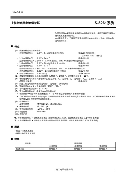
■ 用途
·锂离子可充电电池组 ·锂聚合物可充电电池组
■ 封装
封装名
SOT-23-6
封装图面 MP006-A
图面号码 卷带图面
MP006-A
带卷图面 MP006-A
精工电子有限公司
1
1节电池用电池保护IC S-8261系列
■ 框图
DP
控制输出电路
DO
向 0 V 电池充电可能 或充电禁止电路
分频器 控制逻辑
过电流1 检测电压
[VIOV1] 0.16 V 0.08 V 0.15 V 0.08 V 0.20 V 0.10 V 0.13 V 0.10 V 0.10 V 0.15 V 0.08 V 0.10 V 0.10 V 0.10 V 0.20 V 0.13 V 0.13 V 0.20 V 0.08 V 0.15 V 0.05 V 0.10 V 0.06 V 0.15 V 0.15 V 0.18 V 0.08 V 0.10 V 0.15 V 0.13 V 0.12 V 0.25 V 0.10 V 0.10 V 0.15 V 0.10 V 0.15 V 0.13 V 0.06 V 0.13 V
tIOV2
1.12 ms
负载短路检测延迟时间 tSHORT
―
备注 粗线框内表示为标准产品的延迟时间。
选择范围 1.2 s
144 ms 9 ms
2.24 ms 320 µs
4.6 s 290 ms 18 ms
― 600 µs
备注 从左项中选择 从左项中选择 从左项中选择 从左项中选择 从左项中选择
精工电子有限公司
精度±25 mV(25°C)、
· 过充电滞后电压
0.1 V ~ 0.4 V *1
gdm8261a使用手册

gdm8261a使用手册摘要:1.引言2.gdm8261a 的功能与特点3.安装与配置4.使用方法5.常见问题与解决方法6.结论正文:【引言】欢迎使用gdm8261a!本手册将为您提供全面的使用指南,帮助您充分发挥这款设备的性能。
【gdm8261a 的功能与特点】gdm8261a 是一款功能强大、易于使用的设备,具有以下特点:1.高性能:gdm8261a 采用了先进的技术,能够处理大量数据,提高工作效率。
2.多功能:设备支持多种功能,包括但不限于数据采集、分析、存储等。
3.易于操作:gdm8261a 的界面直观,操作简便,无需专业培训即可上手。
【安装与配置】在开始使用前,请按照以下步骤进行安装与配置:1.检查设备是否完好,确保所有附件齐全。
2.根据设备上的标签,连接相应的线缆。
3.打开设备上的电源开关,启动设备。
4.打开浏览器,输入设备上的IP 地址,登录设备。
【使用方法】在设备启动后,您可以开始使用:1.数据采集:在主界面选择数据采集功能,根据提示设置参数,开始采集数据。
2.数据分析:采集完成后,选择数据分析功能,根据提示进行分析。
3.数据存储:分析完成后,选择数据存储功能,将结果保存到指定位置。
【常见问题与解决方法】在使用过程中,可能会遇到以下问题:1.设备无法启动:请检查线缆连接是否正常,电源是否打开。
2.数据采集失败:请检查参数设置是否正确,线缆连接是否松动。
3.数据分析失败:请检查数据质量是否达标,分析参数是否设置正确。
如遇到问题,请参考本手册或联系售后服务。
【结论】感谢您选择gdm8261a,希望本手册能够帮助您更好地使用这款设备。
如果您在使用过程中遇到任何问题,欢迎随时联系我们。
gdm8261a使用手册
gdm8261a使用手册摘要:1.引言2.gdm8261a 使用手册的概述3.硬件安装与配置4.软件安装与配置5.使用gdm8261a 进行数据采集6.gdm8261a 的数据处理与分析7.常见问题与解决方案8.总结正文:gdm8261a 使用手册提供了详细的硬件和软件安装、配置以及数据采集、处理和分析的步骤。
以下是使用手册的主要内容概述。
1.引言gdm8261a 是一款高性能的数据采集模块,广泛应用于各种数据采集和监测场景。
在使用gdm8261a 之前,请确保已阅读并理解本使用手册的内容。
2.gdm8261a 使用手册的概述本使用手册共分为8 个部分,分别为:引言、硬件安装与配置、软件安装与配置、使用gdm8261a 进行数据采集、gdm8261a 的数据处理与分析、常见问题与解决方案、总结。
用户可以根据需要查阅相应部分的内容。
3.硬件安装与配置本部分介绍了gdm8261a 的硬件组成、连接方式和注意事项。
根据实际应用场景和需求,正确连接gdm8261a 的各部分硬件。
4.软件安装与配置本部分介绍了与gdm8261a 配合使用的软件及其安装方法。
安装完成后,按照说明进行软件配置,以确保与硬件的正确连接。
5.使用gdm8261a 进行数据采集本部分详细介绍了如何使用gdm8261a 进行数据采集。
根据实际需求,设置合适的参数,开始采集数据。
6.gdm8261a 的数据处理与分析本部分介绍了如何对gdm8261a 采集到的数据进行处理和分析。
通过相关软件,可以对数据进行实时监测、存储和分析。
7.常见问题与解决方案本部分列举了在使用gdm8261a 过程中可能遇到的问题及相应的解决方案。
遇到问题时,请先查阅本部分内容,以便及时解决。
8.总结本部分对gdm8261a 使用手册的主要内容进行了总结。
希望本手册能够帮助用户更好地理解和使用gdm8261a。
总之,gdm8261a 使用手册为用户提供了详细的操作指南。
g8261标准
g8261标准G8261标准是一种关于数字电视信号的标准,它规定了数字电视信号的传输、编码和解码等方面的技术要求和规范。
下面将详细介绍G8261标准的主要内容。
一、概述G8261标准是欧洲电信标准化协会(ETSI)发布的一项数字电视标准,旨在提供一种通用的数字电视信号格式,以便在不同国家和地区的数字电视系统中实现互通性和兼容性。
该标准适用于地面、卫星和有线等多种传输方式,能够提供高清晰度电视(HDTV)、标准清晰度电视(SDTV)和普通清晰度电视(LDTV)等多种视频格式。
二、传输方式G8261标准支持地面传输和卫星传输两种方式。
对于地面传输,该标准采用了数字音频广播(DAB)和数字视频广播(DVB)等技术,可以实现高清晰度电视和标准清晰度电视等多种视频格式的传输。
对于卫星传输,该标准采用了DVB-S2等技术,可以实现高速数据传输和高可靠性的信号覆盖。
三、编码方式G8261标准采用了高效视频编码(HEVC)技术,这是一种面向高清和超高清视频的编码技术,可以实现更高的编码效率和更好的图像质量。
HEVC技术可以将视频流压缩成较小的数据量,从而降低传输带宽和存储空间的需求。
同时,HEVC技术还支持多种分辨率和帧率,可以根据实际需求进行灵活的编码和传输。
四、解码方式G8261标准采用了高效的解码技术,可以对接收到的数字电视信号进行快速解码和播放。
该标准支持多种解码方式,包括软件解码和硬件解码等。
软件解码可以通过计算机或嵌入式处理器实现,而硬件解码则可以通过专门的解码芯片或模块实现。
高效的解码技术可以提高数字电视信号的播放质量和流畅度。
五、安全性G8261标准还考虑了数字电视信号的安全性问题。
该标准采用了加密和认证等技术,确保数字电视信号在传输过程中不被篡改或非法接收。
同时,该标准还支持数字版权管理(DRM)等技术,可以保护版权和防止盗版行为。
六、其他特性除了上述主要内容外,G8261标准还具有以下特性:1.灵活性:G8261标准支持多种传输方式和编码方式,可以根据实际需求进行灵活的配置和应用。
- 1、下载文档前请自行甄别文档内容的完整性,平台不提供额外的编辑、内容补充、找答案等附加服务。
- 2、"仅部分预览"的文档,不可在线预览部分如存在完整性等问题,可反馈申请退款(可完整预览的文档不适用该条件!)。
- 3、如文档侵犯您的权益,请联系客服反馈,我们会尽快为您处理(人工客服工作时间:9:00-18:30)。
单节锂离子/锂聚合物电池用保护 IC
DP8261 内置高精度电压检测电路和延迟电路,是用于单节锂离子/锂聚合物可再充电电 池的保护 IC。
本 IC 适合于对 1 节锂离子/锂聚合物可再充电电池的过充电、过放电和过电流进行保护。
1. 特点
DP8261 全系列 IC 具备如下特点:
(1) 高精度电压检测电路
表 5、绝对最大额定值(VSS=0V,Ta=25℃,除非特别说明)
项目
符号
规格
VDD 和 VSS 之间输入电压
VDD
OC 输出端子电压
VOC
OD 输出端子电压
VOD
CS 输入端子电压
VCS
工作温度范围
TOP
储存温度范围
TST
容许功耗
PD
VSS-0.3~VSS+10 VDD-20~VDD+0.3 VSS-0.3~VDD+0.3 VDD-20~VDD+0.3
注意:初次连接电芯时,会有不能放电的可能性,此时,短接 CS 端子和 VSS 端子,或 者连接充电器,就能恢复到正常工作状态。
8.2. 过充电状态 正常工作状态下的电池,在充电过程中,一旦电池电压超过过充电检测电压(VCU),并
且这种状态持续的时间超过过充电检测延迟时间(TOC)以上时,保护 IC 会关闭充电控制用 的 MOSFET(OC 端子),停止充电,这个状态称为“过充电状态”。
VCR
4.080V
4.030
VDL
3.00V
2.95
VDR
3.00V
2.95
VDIP
VDD=3.6V
60
VSIP
VDD=3.0V
0.55
VCIP
VDD=3.6V
-70
控制端子输出电压
VDH
VDD-0.1
VDL
-
VCH
VDD-0.1
VCL
-
向 0V 电池充电的功能(允许或禁止)
V0CH
允许向 0V 电池充电功 能
*2、R2 连接过大电阻,当连接高电压充电器时,有可能导致不能切断充电电流的情况发生。 但为控制充电器反接时的电流,请尽可能选取较大的阻值。 *3、C1有稳定VDD电压的作用,请不要连接0.01μF以下的电容。 *4、使用MOSFET的阈值电压在过放电检测电压以上时,可能导致在过放电保护之前停止放 电。 *5、门极和源极之间耐压在充电器电压以下时,N-MOSFET有可能被损坏。
负载短路检测延迟 时间
TSIP 300μs
3.3. 特性代码-其它功能选择
表 3、特性代码-其它功能选择表
特性代码 A
向 0V 电池充电功能 允许
休眠功能/过放自恢复功能 有休眠功能
2/11
Rev.1.0 AUG 2010
4. 封装、脚位及标记信息
D P8261
单节锂离子/锂聚合物电池用保护 IC
(6) 向 0V 电池充电功能:可以选择
(7) 宽工作温度范围:
-40℃~+85℃
(8) 小型封装:
SOT-23-6
(9) 无卤素绿色环保产品
OC
OD
2. 方框图
振荡器
VDD
电平移动
计数器
允许向0V电池充 电电路或禁止向
0V电池充电电路
逻辑电路
过充电检测比较器
短路检测器
充电过流检测 比较器
过放电检测比较器
1.2
V0IN
禁止向 0V 电池充电功 能
-
4.080 3.00 3.00 75 0.85 -50
VDD-0.02 0.1
VDD-0.02 0.1
-
-
说明:*1、此温度范围内的参数是设计保证值,而非高、低温实测筛选。
最大值
8 20
6.0 0.1
4.305 4.315
4.130 3.05 3.05 90 1.15 -30
-40~+85 -40~+125
250
单位 V V V V ℃ ℃
mW
3/11
Rev.1.0 AUG 2010
D P8261
单节锂离子/锂聚合物电池用保护 IC
6. 电气特性
6.1. 电气参数(延迟时间除外)
表 6、电气参数(延迟时间参数除外。VSS=0V,Ta=25℃,除非特别说明。)
精度±0.3V
(2) 各延迟时间由内部电路设置(不需外接电容)
(3) 休眠功能:有
(4) 低耗电流
z 工作模式
典型值 3.0μA ,最大值 6.0μA(VDD=3.9V)
z 休眠模式
最大值 0.1μA(VDD=2.0V)
(5) 连接充电器的端子采用高耐压设计(CS 端子和 OC 端子,绝对最大额定值是 20V)
0.5
0.5
-
0.5
单位
V V
μA μA
V V
V V V mV V mV
V V V V
V
V
6.2. 延迟时间参数
表 7、延迟时间代码=3 时,延迟时间参数组合
项目 过充电检测延迟时间 过放电检测延迟时间 放电过流检测延迟时间 充电过流检测延迟时间 负载短路检测延迟时间
符号
TOC TOD TDIP TCIP TSIP
项目
VDD-VSS 工作电压 VDD-CS 工作电压
工作电流 过放电时耗电流
符号
VDSOP1 VDSOP2
IDD IOD
条件 输入电压
-
耗电流
VDD=3.9V VDD=2.0V
检测电压
最小值 典型值
1.5
-
1.5
-
-
3.0
-
-
过充电检测电压
4.280V
4.255
VCU
4.280V ( -5℃ ~ 55℃ (*1))
VCU
VCR
4.280V
4.080V
过放电检 测电压
VDL 3.00V
过放电释 放电压
VDR 3.00V
放电过流 检测电压
VDIP 75mV
充电过流 检测电压
VCIP -50mV
延迟时间 代码
3
特性代码
A
1、表 1 中列出各电气参数的典型值,各电气参数的精度请参阅表 6。 2、延迟时间代码对应的延迟时间参数请参阅表 2;特性代码对应的其它功能特性请参阅表 3。 3、需要上述规格以外的产品时,请与本公司业务部联系。
z SOT-23-6 封装
表 4、SOT-23-6 封装
脚位
符号
3
OC
4
NC
5
VDD
6
VSS
说明 放电控制用 MOSFET 门极连接端子 过电流检测输入端子,充电器检测端子 充电控制用 MOSFET 门极连接端子 无连接 电源端,正电源输入端子 接地端,负电源输入端子
5. 绝对最大额定值
放电过流检测比较器 CS
VSS
1/11
Rev.1.0 AUG 2010
3. 产品目录
D P8261
单节锂离子/锂聚合物电池用保护 IC
3.1. 电气参数选择 z SOT-23-6 封装
表 1、电气参数选择表
参数
型号 DP8261-G3J
备注:
过充电检测 过充电释
电压
放电压
4.245
4.280 4.280
过充电释放电压
过放电检测电压 过放电释放电压 放电过流检测电压 负载短路检测电压 充电过流检测电压
OD 端子输出高电压 OD 端子输出低电压 OC 端子输出高电压 OC 端子输出低电压
充电器起始电压(允许 向 0V 电池充电功能) 电池电压(禁止向 0V 电池充电功能)
来控制充电和放电。当电池电压在过放电检测电压(VDL)以上并在过充电检测电压(VCU) 以下,且 CS 端子电压在充电过流检测电压(VCIP)以上并在放电过流检测电压(VDIP)以下 时,IC 的 OC 和 OD 端子都输出高电平,使充电控制用 MOSFET 和放电控制用 MOSFET 同 时导通,这个状态称为“正常工作状态”。此状态下,充电和放电都可以自由进行。
z 过充电检测电压
4.280V
精度±25mV
z 过充电释放电压
4.080V
精度±50mV
z 过放电检测电压
3.00V
精度±50mV
z 过放电释放电压
3.00V
精度±50mV
z 放电过流检测电压 75mV
精度±15mV
z 充电过流检测电压 -50mV
精度±20mV
z 负载短路检测电压 0.85V(固定)
而一旦 CS 端子电压超过负载短路检测电压(VSIP),并且这种状态持续的时间超过负载短 路检测延迟时间(TSIP),则也关闭放电控制用的 MOSFET(OD 端子),停止放电,这个状 态称为“负载短路状态”。
当连接在电池正极(PB+)和电池负极(PB-)之间的阻抗大于放电过流/负载短路释放 阻抗(典型值约 300kΩ)时,放电过流状态和负载短路状态释放,恢复到正常工作状态。另 外,即使连接在电池正极(PB+)和电池负极(PB-)之间的阻抗小于放电过流/负载短路释 放阻抗,当连接上充电器,CS 端子电压降低到放电过流保护电压(VDIP)以下,也会释放放 电过流状态或负载短路状态,回到正常工作状态。
注意: 1. 上述参数有可能不经预告而作更改,请及时到我司网站上下载最新版规格书。 2. 外围器件如需调整,建议客户进行充分的评估和测试。
5/11
Rev.1.0 AUG 2010
D P8261
单节锂离子/锂聚合物电池用保护 IC
