CST MICROWAVE STUDIO-WorkflowandsolverOverview
CST微波工作室学习笔记(3)
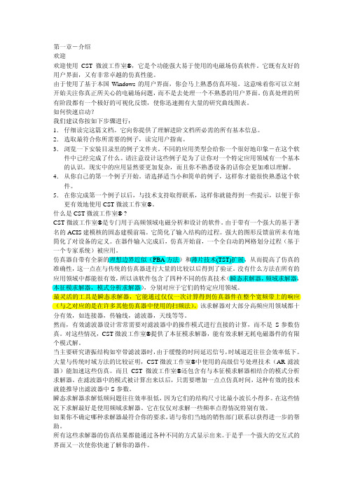
CST微波工作室学习笔记(3)六、边界条件和背景材料为什么要设置边界条件:•使用计算机来进行电磁计算或电磁仿真分析,都是只能处理有限空间内的电磁问题•在CST微波工作室中,通过设置适当的边界条件,实现把电磁问题设定于有限空间内背景概念:•用户创建的结构模型区域以外的空间背景材料•指用户所创建模型的外侧的填充材质背景材料设置•Modeling > Materials > Background•常用材质:PEC(理想导体)、Nomal(空气或真空)、Anisotropic(各向异性)、Lossy Metal(有耗导体)边界条件设置•Simulation > Setting > Boundaries边界条件类型1. Electric(电边界)•等效于理想导体(PEC),电场垂直于边界表面•当背景材料设置为理想导体时,自动设置为电边界•2. Magnetic(磁边界)•边界条件上的电场方向与表面相切,磁场垂直于边界表面•-实际上不存在理想磁边界,只是理论上的约束条件•3. Open(PML)(开放边界)•相当于理想匹配层(PML),电磁波几乎无反射通过该边界•可用于等效自由空间情况4. Open(add space)•与 Open 边界条件相同,边界表面设置与模型有一定的距离,主要是用于远区场的计算•用于天线、RCS等辐射/散射问题的仿真分析5. Periodic(周期性边界条件)•用于阵列天线、FSS等周期性结构的仿真分析•成对出现、需要设置相位差6. Counducting wall(有耗导体边界条件)•良导体/非理想导体边界条件,等效于有耗导体,电场垂直边界表面•当背景材料设置为有耗导体(lossy metal),自动设置为有耗导体边界•7. Unit Cell(用于周期性问题求解的边界条件)•类似周期边界条件、用于周期性结构的仿真分析•只能用于通用频域求解器8. Symmetry Planes(设置对称面的边界条件)•应用对称边界构造结构时仅构造一部分,减小结构尺寸和设计复杂性、缩短计算时间•有电壁对称面、磁壁对称面两种类型•电场垂直对称面且对称,选择电壁对称面•磁场垂直对称面且对称,选择磁壁对称面••七、端口和激励详解•激励•指在进行仿真分析时需要提供的激励信号源•在CST微波工作室中,提供了多种不同类型的激励源,用于分析不同类型问题•在运行仿真分析之前,至少要设置一个激励源作为结构的输入信号激励•激励类型•- 端口激励(Port):可以分析给出的S参数、也可分析给出场分布•——离散端口(Discrete Ports)•——波导端口(Waveguide Ports)•- 场源激励(Field Source):只能分析给出场分布•——平面波激励(Plane Waves)•——远区场激励(Farfield Sources)•——近区场激励(Nearfield Sources)••负载——集总元件(Lumped Element)••1.波导端口——Waveguide Ports•什么是波导端口•模拟一段连接在结构模型上的无限长的波导,因为波导端口模式匹配良好,几乎能全部吸收结构模型内传输过来的电磁波,从而达到很高的仿真精度•波导端口默认的输入激励信号功率是1W•设置操作和端口对话框•General:设置端口的名称等•Position:设置端口的位置坐标•Reference plane:设置端口位于模型外部或内部位置••应用范围•波导结构模型•同轴线结构模型•微带线/带状线/共面波导等传输线结构模型•2.离散端口——Discrete Ports•什么是离散端口•离散端口是由具有内阻的电流源组成,设置于结构模型内部•定义更简单,只需要定义域结构相连的两个管脚即可•端口的电长度最好小于1/10个波长,否则仿真结果相差大•离散端口设置•离散棱边端口(选中两个端口表面进行设置)•离散表面端口(选中两个棱边进行设置)•Properties:设置激励源类型、端口名称、内阻等•Location:设置端口的坐标••3.平面波激励——Plane Waves•模拟从无限远处发射过来的电磁波激励,主要用于RCS一类的散射问题的分析•只分析远区场,不计算S参数•需要设置开放边界条件(Open)••4.远区场激励——Farfield Sources•把在其他微波工作室分析出的远区场导入到另一个微波工作室中用作激励源•5.近区场激励——Nearfield Sources•把在其他微波工作室分析出的近区场导入到另一个微波工作室中用作激励源•波导端口平面设置•波导结构••同轴线结构••微带线•端口需要足够大以覆盖准TEM模的重要部分••另一方面,端口又不能太大,会激发高次模••如果激发高次模,造成时域求解器能力衰减十分缓慢,频谱结果会看到非常多的毛刺•分析完成后,查看端口处的场分布,确认端口大小是后合适••共面线/共面波导•不接地共面线和接地共面线••模式数••负载——Lumped Element•Type:电阻、电感、电容串联;电阻、电感、电容并联;二极管等;•R:电阻大小•L:电感大小•C:电容大小•Location:定义各器件所在坐标••八、求解器详解•- 求解器的分类•Time Domain Solver——时域求解器•Frequency Domain Solver——频域求解器•Eigenmode Solver——本征模求解器•Integral Equation Solver——积分方程求解器•Asymptomatic Solver——高频渐进求解器•Multilayer Solver——多层平面矩量法求解器••- 电尺寸的定义•是物体的几何尺寸除以波长,单位为波长;电尺寸小于5个波长称为电小;大于5小于50称为电中;大于50小于500称为电大;大于500称为超电大•- 计算电磁学的电磁数值算法•全波算法(精确算法):分为时域全波和频域全波算法,直接求解麦克斯韦积分或微分方程。
(完整版)CST使用教程

1.1 软件介绍CST公司总部位于德国达姆施塔特市,成立于1992年。
它是一家专业电磁场仿真软件的提供商。
CST软件采用有限积分法(Finite Integration)。
其主要软件产品有:CST微波工作室——三维无源高频电磁场仿真软件包(S参量和天线)CST设计工作室——微波网络(有源及无源)仿真软件平台(微波放大器、混频器、谐波分析等)CST电磁工作室——三维静场及慢变场仿真软件包(电磁铁、变压器、交流接触器等)马飞亚(MAFIA)——通用大型全频段、二维及三维电磁场仿真软件包(包含静电场、准静场、简谐场、本振场、瞬态场、带电粒子与电磁场的自恰相互作用、热动力学场等模块)在此,我们主要讨论“CST微波工作室”,它是一款无源微波器件及天线仿真软件,可以仿真耦合器、滤波器、环流器、隔离器、谐振腔、平面结构、连接器、电磁兼容、IC封装及各类天线和天线阵列,能够给出S参量、天线方向图等结果。
1.2 软件的基本操作1.2.1 软件界面启动软件后,可以看到如下窗口:1.2.2 用户界面介绍1.2.3 基本操作1).模板的选择CST MWS内建了数种模板,每种模板对特定的器件类型都定义了合适的参数,选用适合自己情况的模板,可以节省设置时间提高效率,对新手特别适用,所有设置在仿真过程中随时都可以进行修改,熟练者亦可不使用模板模板选取方式:1,创建新项目 File—new2,随时选用模板 File—select template模板参数模板类型2)设置工作平面首先设置工作平面(E dit-working Plane Properties)将捕捉间距改为 1以下步骤可遵循仿真向导(Help->QuickStart Guide)依次进行1)设置单位(Solve->Units)合适的单位可以减少数据输入的工作量2)能够创建的基本模型3)改变视角快捷键为:视觉效果的改变:4)几何变换四种变换:5)图形的布尔操作四种布尔操作:例如:这里以“减”来说明具体操作1,两种不同材料的物体2,选择第一个物体(立方体)3点击工具栏上的图标或在主菜单选择Objects->Boolean->Subtract 4,选择第二个物体(圆球)5,回车确定6)选取模型的点、边、面对每种“选取操作”,都必须选择相应的选取工具。
CST微波工作室视频培训教程讲义—求解器

CST微波工作室视频培训教程讲义—求解器CST Microwave Studio(CST MWS)是一款专门设计用于高频电磁仿真的软件工具。
在使用CST MWS进行仿真时,求解器是非常重要的组成部分。
求解器是用于对电磁场进行数值求解的算法模块,其性能和精度直接影响到仿真结果的准确性和计算效率。
本教程将重点介绍CST MWS中常用的求解器及其参数设置方法,帮助读者更好地理解求解器的工作原理和优化仿真计算。
一、求解器的选择CSTMWS提供了多种求解器可供选择,包括时域求解器、频域求解器和热仿真求解器等。
不同的求解器适用于不同的仿真场景,读者在使用CSTMWS时应根据具体的仿真需求选择合适的求解器。
1.时域求解器(TDS)时域求解器适用于处理时间域中包含脉冲信号的仿真问题,如脉冲天线、雷达系统等。
时域求解器可以直接求解电磁场在时域中的分布情况,精度高、计算效率较高。
在使用时域求解器时,读者需要注意设置时间步长和仿真时间范围等参数。
2.频域求解器(FDS)频域求解器适用于处理频率域中的电磁仿真问题,如天线阵列、微波滤波器等。
频域求解器可以求解电磁场在频域中的分布情况,精度高、适用于高频和复杂结构的仿真问题。
在使用频域求解器时,读者需要注意设置频率范围和网格密度等参数。
3.热仿真求解器热仿真求解器适用于处理包含热耦合效应的电磁仿真问题,如微波加热、热辐射传热等。
热仿真求解器可以求解电磁场与温度场之间的相互作用关系,帮助用户分析电磁场对材料的热效应。
在使用热仿真求解器时,读者需要注意设置材料参数和热边界条件等参数。
二、求解器参数设置在使用CSTMWS进行仿真时,读者需要注意合理设置求解器的参数,以保证仿真结果的准确性和计算效率。
以下是一些常用的求解器参数设置方法:1.网格密度网格密度是求解器计算的基本要素,直接影响到仿真结果的准确性和计算效率。
通常情况下,网格密度越高,仿真结果越准确,但计算速度也会变慢。
在设置网格密度时,读者可以根据仿真对象的几何结构和电磁特性合理选择网格大小和分割方式。
cst微波工作室算法 -回复

cst微波工作室算法-回复CST微波工作室算法:全面解读及应用【引言】近年来,随着电磁场计算算法和计算机硬件的飞速发展,CST微波工作室算法成为了解决电磁场计算问题的一种重要工具。
本文将一步一步地讲解CST微波工作室算法的相关内容,介绍其基本原理、主要功能以及典型应用案例。
【基础知识】在深入了解CST微波工作室算法之前,我们先来简要了解一下相关基础知识。
CST微波工作室算法是一种用于解决微波电磁场计算问题的数值模拟方法。
其核心思想是基于麦克斯韦方程组,在有限的空间范围内将对电磁场的求解问题转化为离散的数值计算问题。
【基本原理】CST微波工作室算法的基本原理可以分为以下几个步骤:1. 几何建模:首先,根据实际问题,使用CAD软件对待模拟的物理结构进行几何建模。
这一步骤非常重要,几何模型的准确性直接影响到后续的计算结果。
2. 网格划分:在进行数值计算之前,需要将几何模型离散化成为有限个小单元的集合,即网格划分。
不同的结构和精度要求会影响网格的划分方式和密度。
3. 边界条件设置:在离散化后的网格中,边界条件的设置是十分关键的一步。
边界条件的选择应根据实际问题和模型的特点来确定。
4. 方程求解:通过数值方法对麦克斯韦方程组进行求解。
CST微波工作室算法可以通过有限差分法(FDTD)、FEM(有限元法)等一系列数值求解方法来解决问题。
5. 结果分析与后处理:完成方程的求解后,对计算结果进行分析和后处理。
CST微波工作室算法提供了丰富的分析功能,如电场分布、功率传输、散射特性等。
【主要功能】CST微波工作室算法具有以下主要功能:1. 电场分析:通过计算麦克斯韦方程组,可以获得电场在空间中的分布情况。
这对于分析电场的强度、分布及它们对周围物体的影响是十分重要的。
2. 功率传输分析:CST微波工作室算法能够对微波、光纤等传输线路的功率传输情况进行仿真分析,包括传输损耗、传输特性等。
3. 散射特性分析:通过CST微波工作室算法,可以对各种物体的散射特性进行分析,如反射、透射、散射等。
CST微波工作室视频培训教程讲义—求解器
微波EDA网() | 专注于微波射频培训
CST微波工作室求解器简介(cont.)
本征模求解器—— Eigenmode Solver
• 本征模求解器用来计算封闭器件内的谐振场分布, CST微波工作室提供了AKS和JDM两种算法的本征 模求解器
微波EDA网() | 专注于微波射频培训
计算电磁学中的几个基本概念
电尺寸的概念和电大、电中、电小尺寸的划分
• 电尺寸的定义是物体的几何尺寸除以波长,单位为波长。如一辆4.5米的小轿车,对于1GHz的频率,其 电尺寸是15个波长;而对于3GHz的频率,其电尺寸是45个波长;
• Monitors—设置要计算场分布的频点 • Single、Automatic、Equidistant、Logarithmic
设置频点分布类型
• Use Broadband frequency sweep
CST一种特殊宽带扫频技术,能以较少的频点数 得出整个频带内的扫频性能
• 通用设置
Automatic + Use Broadband frequency sweep, 这样求解器自动选择频点,能以最少的频点得到 整个频带内的扫频性能
Source Type和Mode
• 设置要分析的端口和模式
微波EDA网() | 专注于微波射频培训
时域求解器——相关设置 (cont.)
S-parameter setting
• 设置S参数的归一化阻抗和互易性
Adaptive mesh refinement
• 设置自适应网格剖分,提高分析结果的准确度
• 高频渐进算法:物理光学法(PO) 、弹跳射线法(SBR)
CST新手入门
关于这本手册 这本手册是用来快速上手 CST 微波工作室®的。它只是让你对主要概念有个总的印象,而 不是针对所有概念的完全参考手册。 理解这些概念有助于你在在线文档帮助下有效地使用该 软件。 该手册的主要部分是被称为快速浏览(第二章)的部分,能指导你熟悉 CST 微波工作室® 的最重要特征。我们强烈建议你仔细研究该章节。 文档约定 在主窗口中输入的命令按如下方式打印: menu bar item ⇒ menu item。这意味着你得先按下“menu ba item”(如“File”)然 后在打开的菜单中选择相应的“menu item”(如“Open”)。 在对话框中需要按下的按钮总是用斜体字表示,如 Ok 。 组合键总是带有一个加(+)号。Ctrl+S 表示你需要在按下“Ctrl”键的同时按下“S” 键。 你的反馈 我 们 一 直 在努 力 提 高 文档 的 质 量 。如 果 你 对 该文 档 有 什 么建 议 , 请 把它 们 发 送 到: support@cst.de
对 SAR 分布的计算 将离散器件(集总参数电阻)做为端口 为 EMC 问题提供理想电压和电流源 在结构任何位置的集总参数的 R、L、C、(非线性)二级管器件 在 TDR 分析中的矩形腔激励 用户定义的激励函数 对级连 SPICE(R,L,C,G)网络模型的自动参数提取。通过运行 SPICE 对结果进 行确认 通过内建的参数扫描工具自动进行参数研究 通过内建的优化器对任意目标自动进行结构优化 频域求解器 对无耗和有耗结构的有效计算 各向同性和各向异性的材料特性 自适应频率采样以便于自动扫频 用户定义扫频 在频域通过 2D 本征模求解器计算端口模式 对指定阻抗重新归一化 S-参数 显式的 S-参数相位 高性能辐射/吸收边界条件 包括相移的周期化边界条件 天线远场计算(包括增益,方向性,旁瓣衰减等等) 天线阵列远场计算 各种电磁量的计算诸如:电场和磁场 将离散器件(集总参数电阻)做为端口 在结构任何位置的集总参数的 R、L、C 元件 对级连 SPICE(R,L,C,G)网络模型的自动参数提取。通过运行 SPICE 对结果进 行确认 本征模求解器 对封闭、无耗结构中模式场分布的计算 各向同性和各向异性的材料 在一台 PC 中最多可使用 2 个处理器进行并行化处理 包括相移的周期化边界条件 对各种模式的损耗和 Q 值的计算(混和方法) 通过内建的参数扫描工具自动进行参数研究 通过内建的优化器对任何目标自动进行结构优化 模式分析仿真器 在使用本征模求解器求得的模式场分布中计算宽频带 S-参数 各向同性和各向异性的材料 在一台 PC 中最多可使用 2 个处理器进行并行化处理 对指定阻抗重新归一化 S-参数 显式的 S-参数相位 对各种模式的损耗和 Q 值的计算(混和方法) 对级连 SPICE(R,L,C,G)网络模型的自动参数提取。通过运行 SPICE 对结果进 行确认
CST微波工作室视频培训教程讲义—求解器
设置频点分布类型
• Use Broadband frequency sweep
CST一种特殊宽带扫频技术,能以较少的频点数 得出Fra bibliotek个频带内的扫频性能
• 通用设置
Automatic + Use Broadband frequency sweep, 这样求解器自动选择频点,能以最少的频点得到 整个频带内的扫频性能
• 主要应用于强谐振结构、腔体、窄带等问题的分析
积分方程求解器—— Integral Equation Solver
• 积分方程求解器是CST较新引入的求解器(2006版引入),其采用多层快速多极子法(MLFMM),主 要用于求解电大尺寸的结构的辐射和散射问题,可分析的结构尺寸可以达到几十甚至几百个波长,应 用范围包含天线辐射、多天线的EMC/互扰分析、天线布局优化和目标物体的RCS研究
微波EDA网() | 专注于微波射频培训
计算电磁学中的几个基本概念
电尺寸的概念和电大、电中、电小尺寸的划分
• 电尺寸的定义是物体的几何尺寸除以波长,单位为波长。如一辆4.5米的小轿车,对于1GHz的频率,其 电尺寸是15个波长;而对于3GHz的频率,其电尺寸是45个波长;
Mesh Type • Hexahedral—采用有限积分法的瞬态时域求解器 • Hexahedral TLM —采用传输矩阵法的TLM时域求解器
Accuracy • 用于设置求解精度 • 瞬态时域求解器以1W功率的高斯脉冲信号对结构进 行激励,当信号能量衰减到趋于零时,分析结束。 其中,结束时的能量和激励信号能量之比就是在此 处Accuracy项设置的值 • 影响仿真分析的时间和求解精度
各大仿真软件介绍(包括算法,原理)
本文由092011235贡献doc文档可能在WAP端浏览体验不佳。
建议您优先选择TXT,或下载源文件到本机查看。
各大仿真软件介绍(包括算法,原理)各大仿真软件介绍(包括算法,原理)声明:以下全来自于网络随着无线和有线设计向更高频率的发展和电路复杂性的增加,对于高频电磁场的仿真,由于忽略了高阶传播模式而引起仿真的误差。
另外,传统模式等效电路分析方法的限制,与频率相关电容、电感元件等效模型而引起的误差。
例如,在分析微带线时,许多易于出错的无源模式是由于微带线或带状线的交叉、阶梯、弯曲、开路、缝隙等等,在这种情况下是多模传输。
为此,通常采用全波电磁仿真技术去分析电路结构,通过电路仿真得到准确的非连续模式 S 参数。
这些 EDA 仿真软件与电磁场的数值解法密切相关的,不同的仿真软件是根据不同的数值分析方法来进行仿真的。
通常,数值解法分为显示和隐示算法,隐示算法(包括所有的频域方法)随着问题的增加,表现出强烈的非线性。
显示算法(例如 FDTD、 FIT 方法在处理问题时表现出合理的存储容量和时间。
本文根据电磁仿真工具所采用的数值解法进行分类,对常用的微波 EDA 仿真软件进行论述。
2.基于矩量法仿真的微波 EDA 仿真软件基于矩量法仿真的 EDA 软件主要包括 ADS(Advanced Design System)、Sonnet 电磁仿真软件、IE3D 和 Microwave office。
2.1 ADS 仿真软件 Agilent ADS(Advanced Design System)软件是在 HP EESOF 系列 EDA 软件基础上发展完善起来的大型综合设计软件,是美国安捷伦公司开发的大型综合设计软件,是为系统和电路工程师提供的可开发各种形式的射频设计,对于通信和航天/防御的应用,从最简单到最复杂,从离散射频/微波模块到集成MMIC。
从电路元件的仿真,模式识别的提取,新的仿真技术提供了高性能的仿真特性。
CST微波工作室视频培训教程讲义—求解器
CST微波工作室视频培训教程讲义—求解器CST Microwave Studio Video Training Course Lecture – Solver 一、简介
CST Microwave Studio 求解器是一个功能强大的电磁求解器,它主
要用于求解高周波电磁问题,可以以2D和3D空间为计算域,同时可以满
足多种不同的应用。
这个部分将展示CST Microwave Studio强大的求解
器如何被用来模拟电磁场和电磁测量。
1.1应用程序
CST Microwave Studio求解器可以用来模拟高周波电磁问题,它可
以满足各种不同的应用,包括吸波体、电磁护罩、射频和微波技术、微波
传感器、飞机电磁设计、射频综合电路、嵌入式电路等。
1.2求解器核心
CST Microwave Studio求解器的核心组件是一系列先进的求解算法,包括有限元法(FEM)、有限差分法(FDM)、有限元-有限差分法(FEM-FDM)和有限元-本构法(FEM-BEM)。
根据应用需求,CST Microwave Studio求解器可以结合这些算法,构成不同的分析模式:比如绝缘体模式、护罩模式、互耦模式等。
1.3运行设置
使用CST Microwave Studio求解器进行模拟前,需要先对模型进行
一些基本的设置,以便更好地满足模拟需求,这些设置可以由CST Microwave Studio的用户可视化界面完成,包括网格划分、增强块的设置、材料参数设定等。
1.4后处理
使用CST Microwave Studio求解器计算完成后,通常需要进行一些后处理。
如何用CST分析同轴线

CST Microwave Studio同轴线S参数(0—10GHz)的仿真过程简介一、打开软件,出现正常操作界面。
二、我们首先进行的是“建模”。
1、定义常用单位。
例如我们可以把长度单位定义为“mm”,把频率单位定义为“GHz”。
操作过程如下:图1如图1,点击“Solve”-- 选择“Units…”,即可弹出如下对话框(图2),在其中选择“mm”和“GHz”。
点击“OK”即完成“单位”的设置。
(图2)2、设置同轴线的外导体如图3中,我们首先建立一个中空的圆柱,将其定义为金属,来作为我们同轴线的外导体。
具体做法如下:a、如图3中,依次点击“Objects”-→”Basic Shapes”--→”Cylinder..”b、或直接“Cylinder”的快捷键(下图黑色圈中)图 33、选择“Cylinder”后,软件要求你连续点击(双击)不同的点,来确定空心圆柱的位置,这时弹出新的“Cylinder”对话框(图4);或在选择“Cylinder”后,之间按计算机的“Esc”键,直接弹出新的“Cylinder”对话框(图4)。
我们可以在此对话框中输入圆柱的内外图 4半径和圆柱的高度。
空心圆柱的外半经为4,内半径为3.5,高度为20。
名称为“cylinder_1”。
通过下面的步骤4来定义它的材料属性。
4、定义材料(层)属性。
在图4中,我们可以通过选择最下面的“New…”,来打开定义材料的对话框(图5)。
在“Layer name:”中输入我们此材料的名称“pec”,在“Type”中选择“PEC”,pec是英文“p erfect e lectricc onductor”缩写。
在图5的左下角,可以选择我们所定义材料的颜色。
图 5关闭对话框5、对话框4即完成“空心圆柱“的建模。
5、同样,如步骤3,我们建立同轴线的内导体,命名为“cylinder_2”,材料也选择金属pec。
我们进行如下参数设置:圆柱cylinder_2的外半径为1.5,内半径为o,长度也为20。
CST微波工作室(CST Microwave Studio)中网格划分(Mesh)和波导端口(Waveguide Port)
摘要—本文简述了在CST微波工作室(CST Microwave Studio)中网格划分(Mesh)和波导端口(Waveguide Port)设立时的基本原理。
针对常见的微波器件结构,简单论述了CST建议的网格划分方法。
简要分析波导端口设置时需要注意的网格长度设置原则。
索引词—CST、仿真I. 简述CST工作室套件(CST Studio Suite)因为多种类的组件和良好的技术支持已经成为很多微波从业者首选的电磁仿真工具。
在使用CST微波工作室(CST Microwave Studio)的过程中,一些使用者在网格划分(Mesh)时会觉得相对比较难于理解和掌握相关的原理和技巧。
也有不少使用者在创建波导端口(Waveguide Port)时会遇到一些错误提示信息。
本文集于CST微波工作室的帮助文件作提供的官方信息,结合作者的使用经验,就上面两个问题作简单的论述与分析。
本部分设定了隐藏,您已回复过了,以下是隐藏的内容II. 网格划分A. 网格划分基本原则CST工作室套件使用有限积分法(Finite Integration Technique)求解麦柯斯韦方程(Maxwell’s Grid Equations)来进行仿真运算[1],因此,每一个创建的模型都要“翻译”成软件可识别的离散结构,这个“翻译”过程通过网格划分(Mesh Generati on)来实现。
在实际操作中,当一个模型创建好的时候,CST专家系统(Expert System)已经按照默认设置作了初始网格划分,这个初始设置可以打开全局网格设置(Global Mesh Pro perties)来查看。
在不应用任何模板(Template)的前提下,每波长网格线数(Line s per wavelength)、最小网格限制(Lower mesh limit)和网格线比率限制(Mesh l ine ratio limit)这三个参数都为10。
关于这三个参数的意义,鉴于篇幅的原因,这里不再详细阐述,有兴趣的读者请参考CST帮助文件[2]。
CST微波工作室--用户全书

CST微波工作室--用户全书目录I 目录卷一基础入门第一章概述 (3)欢迎 (3)如何快速起步? (3)CST微波工作室?的功用为何? (3)谁应使用CST微波工作室?? (4)CST微波工作室?的主要特点 (5)概要 (5)结构建模 (5)瞬态求解器 (6)频域求解器 (7)本征模求解器 (8)模式分析求解器 (8)结果显示及导出结果的计算 (8)导出结果 (9)自动操作 (9)关于本卷 (9)版式约定 (9)您的反馈 (10)联系CST China (10)CST China (10)CST总部 (10)技术支持 (11)第二章安装 (12)安装需求 (12)IICST微波工作室?用户全书(卷一/卷二)软件需求 (12)硬件需求 (12)License选项 (12)安装指南 (13)提供密码文件 (14)第三章快速演练 (15)启动软件 (15)用户界面概览 (16)创建并观察一些简单结构 (17)创建第一个“方块” (17)常用基本图形概述 (19)选择预先定义的图形、用组件来将图形分组和指定材料特性 (20) 改变视角 (23)几何变换 (25)使用布尔操作来合并图形 (28)选取模型的点、边、面 (30)倒直角和倒圆角 (31)拉伸、旋转和渐变 (32)局部坐标系 (38)历史记录 (41)历史树 (43)创建曲线 (45)局部修改 (48)创建平面导线 (50)第一个应用实例 (52)结构 (52)启动CST微波工作室? (53)打开仿真向导 (53)定义单位 (54)定义背景材料 (55)结构建模 (55)定义端口 (62)定义频率范围 (64)目录III定义边界条件和对称面 (64)查看网格 (67)开始仿真 (68)分析端口模式 (70)分析S参量 (71)自适应网格加密 (73)分析各频率的电磁场 (77)参量化模型和自动优化结构 (80)总结 (95)应该选用哪个求解器? (95)天线计算 (98)数字信号激励 (101)频域计算 (104)本征模(谐振器)计算 (106)模式分析计算 (109)离散端口 (110)提取SPICE网络模型 (111)基于模型降阶法的网络参量提取 (112)基于传输线的网络参量提取 (115)第四章寻求更多信息 (119)仿真向导 (119)教程 (120)实例 (121)在线帮助 (121)参见《CST微波工作室?用户全书》(卷三:高级概念) (121) 寻求技术支持 (122)宏语言文档 (122)版本更新记录 (122)附录快捷键一览表 (123)IVCST微波工作室?用户全书(卷一/卷二)主结构视图中的通用快捷键 (123)编辑栏可用快捷键 (126)卷二应用算例第一章魔T (129)几何建模及求解器设置 (130)概述及模型尺寸 (130)几何建模 (131)结果 (140)1D结果(端口信号,S参量) (140)2D和3D结果(端口模式及场监视器) (141)精度分析 (143)获取更多信息 (146)第二章同轴连接器 (147)几何建模及求解器设置 (148)概述及模型尺寸 (148)几何建模 (148)设置求解器并计算S参量 (167)结果 (173)1D结果(端口信号,S参量) (173)2D和3D结果(端口模式及场监视器) (174)精度分析 (176)获取更多信息 (179)第三章微带相桥 (180)几何建模及求解器设置 (181)概述及模型尺寸 (181)目录V 几何建模 (182)结果 (200)1D结果(端口信号,S参量) (200)2D和3D结果(端口模式及场监视器) (202)精度分析 (203)获取更多信息 (206)第四章贴片天线 (208)几何建模及求解器设置 (209)概述及模型尺寸 (209)几何建模 (209)结果 (223)1D结果(端口信号,S参量) (224)2D和3D结果(端口模式及远场监视器) (225)计算天线阵 (227)精度分析 (230)贴片天线阵 (232)几何建模步骤 (232)合并结果 (235)并行激励 (238)获取更多信息 (241)第五章腔体 (242)几何建模及求解器设置 (243)概述及模型尺寸 (243)几何建模 (244)求解器设置 (250)使用AKS的本征模计算 (252)查看本征模式及计算Q值 (256)精度分析 (258)VICST微波工作室?用户全书(卷一/卷二)使用JD(无耗)的本征模计算 (263)获取更多信息 (266)第六章窄带滤波器 (267)几何建模及求解器设置 (268)概述及模型尺寸 (268)几何建模 (269)设置求解器并计算S参量 (282)结果 (291)1D 结果(S参量) (291)2D和3D结果(端口模式和三维模式) (291) 精度分析 (293)其他可选的求解器 (298)JD(无耗)本征模求解器 (298)频域求解器 (301)获取更多信息 (303)。
CST电磁仿真应用的工作站配置方案

CST电磁仿真GPU并行计算工作站配置大全CST MICROWAVE STUDIO 是为快速、精确仿真电磁场高频问题而专门开发的EDA工具,是基于X86架构Windows/Linux环境下的电磁仿真仿真软件。
CST MICROWAVE STUDIO 是市场和技术领先的全时域高频电磁场仿真求解器, 它基于有限积分法(Finite Integration Technique,简称FIT). 伴随着CST的理想边界拟合(PERFECT BOUNDARY APPROXIMATION,简称PBA)专利技术, CST MWS 通过保形法和有效实施的精确性,提供前所未有的性能. 现在每一个使用者可以借助GPU计算技术大幅缩短求解时间和对更大规模网络单元求解计算.CST MICROWAVE STUDIO的GPU计算模式在运行仿真计算之前,GPU计算需要通过 CST Microwave Studio接口打开开关XASUN超级计算机—集高性能、高可靠、超静音、完美配置于一身XASUN 高端定制图形工作站是专门为行业应用软件量身定制的高性能计算机,产品包括服务器、工作站、高速存储、集群系统等系列,和传统工作站相比,在高性能计算、CAD/CAM/ CAE、动画渲染、虚拟仿真、影视后期、数据库应用、视觉计算等领域,最大限度限度满足应用软件硬件要求.采用最先进技术与架构,彻底消除CPU、内存、硬盘、GPU在性能、容量、带宽的瓶颈提供最合理硬件配置,确保应用软件完美运行, 更环保, 更安静下面是XASUN配备Nvidia GT200核心架构Tesla GPU处理器,为CST各种规模求解,打造的高性能工作站配置方案1.中小规模电磁仿真的工作站配置求解规模: 4000万网格单元以内工作站配置要求:CPU Core i7 920/940/965/975内存12GB DDR3 1333显卡Quadro FX580GPU Nvidia Tesla C1060硬盘SATA 500G 以上7200转或1万转,可选RAID0、5操作系统Windows 7 (X64),Window Server 2008 (X64) ,Linux AS5(X64) 240核XASUN G1并行超算仿真工作站型号XASUN G1 P11712TA2.中大规模电磁仿真的工作站配置求解规模: 8000万网格单元以内工作站配置要求:CPU 双路四核Xeon X5550 X5560 X5570GPU 2*Tesla C1060内存24~96GB DDR3 -1333 Ecc Reg显卡Quadro FX1800/Quadro FX3800硬盘SAS 300G 15000转,可选RAID0、5SATA 32MB 500G 7200转,可选RAID 0、10 操作系统Windows XP 64位SP2 中文版480核XASUN G2并行超算仿真工作站型号XASUN G2 T22425TB3.超大规模电磁仿真的工作站配置求解规模: 1亿6000万网格单元以内工作站配置要求:CPU 双路六核Xeon X5650 ~X5680内存48G~192G DDR3 -1333 Ecc Reg显卡Quadro FX3800/Quadro FX4800/Quadro FX5800 硬盘SAS 450G 15000转,可选RAID0、5、10阵列卡硬SAS高速阵列卡操作系统Windows XP 64位SP2 中文版960核XASUN G4并行超算仿真工作站型号XASUN G4 T22748AC标准配置:。
CST DESIGN STUDIO - Workflow
CST STUDIO SUITE™ 2010Workflow CST DESIGN STUDIO™Copyright© CST 2001-2010CST – Computer Simulation Technology AGAll rights reserved.Information in this document is subject to change without notice. The software described in this document is furnished under a license agreement or non-disclosure agreement. The software may be used only in accordance with the terms of those agreements.No part of this documentation may be reproduced, stored in a retrieval system, or transmitted in any form or any means electronic or mechanical, including photocopying and recording, for any purpose other than the purchaser’s personal use without the written permission of CST. TrademarksCST STUDIO SUITE, CST MICROWAVE STUDIO, CST EM STUDIO, CST PARTICLE STUDIO, CST CABLE STUDIO, CST PCB STUDIO, CST MPHYSICS STUDIO, CST MICROSTRIPES, CST DESIGN STUDIO, CST are trademarks or registered trademarks of CST AG. Other brands and their products are trademarks or registered trademarks of their respective holders and should be noted as such.CST – Computer Simulation Technology AG ContentsCHAPTER 1 — INTRODUCTION (3)Welcome (3)How to Get Started Quickly (3)What is CST DESIGN STUDIO? (4)Main applications for CST DESIGN STUDIO (4)CST DESIGN STUDIO Key Features (5)User Interface (5)Components / Circuit Models (5)Analysis (5)Visualization (6)Documentation (6)Automation (6)About This Manual (7)Document Conventions (7)Your Feedback (7)CHAPTER 2 — QUICK TOUR (8)Overview of the User Interface’s Structure (8)Overview of Available Components (11)Components or Circuit Models (11)External Ports (11)Probes (11)Creating a System (12)Adding and Connecting Components (12)Changing Properties of a Block (16)Changing Properties of an External Port (18)Performing a Simulation (20)Unit Settings (20)Defining Simulation Tasks (21)Starting a Simulation (24)Visualization of the Results (25)Standard Results (25)Customizing Result View Properties (29)User-Defined Result Views (31)Parameterization and Optimization (33)Using Parameters (33)Performing a Parameter Sweep (38)Performing an Optimization (43)CHAPTER 3 — INTEGRATION WITH CST MICROWAVE STUDIO (53)Integration from the CST MICROWAVE STUDIO User’s Point of View (53)Transient EM/Circuit Co-Simulation (59)Integration from the CST DESIGN STUDIO User’s Point of View (62)Example Introduction (62)CST MICROWAVE STUDIO Models (63)CST DESIGN STUDIO Modeling (66)CST DESIGN STUDIO Simulation (69)Optimization (74)Antenna Calculation (77)CHAPTER 4 — INTEGRATION WITH CST MICROSTRIPES (81)Integration from the CST MICROSTRIPES User’s Point of View (81)Integration from the CST DESIGN STUDIO User’s Point of View (81)CHAPTER 5 — INTEGRATION WITH CST PCB STUDIO AND CST CABLE STUDIO (84)Integration from the CST PCB STUDIO / CST CABLE STUDIO User’s Point of View (84)Integration from the CST DESIGN STUDIO User’s Point of View (85)CHAPTER 6 – FINDING FURTHER INFORMATION (87)Online Reference Documentation (87)Examples (87)Access Technical Support (87)Macro Language Documentation (88)History of Changes (88)Chapter 1 — IntroductionWelcomeWelcome to CST DESIGN STUDIO™, the powerful and easy-to-use schematic design tool built for fast synthesis and optimization of complex systems. The tight integration with CST MICROWAVE STUDIO®, CST MICROSTRIPES™, CST PCB STUDIO™ and CST CABLE STUDIO™, our electromagnetic field simulators, and the integration of best-in-class solutions for 2½D electromagnetic planar analysis from different vendors allow you to consider your system at different levels and take into account various effects.CST DESIGN STUDIO™ is part of the CST STUDIO SUITE™. Please refer to the CST STUDIO SUITE™Getting Started manual first. The following explanations assume that you already installed the software and familiarized yourself with the basic concepts of the user interface.Within CST STUDIO SUITE™, CST DESIGN STUDIO™ appears in two different ‘flavors’:•As a stand-alone tool. It runs independently, without any connections to a specific field simulator project.•As an associated view to a CST MICROWAVE STUDIO®, CST MICROSTRIPES™, CST PCB STUDIO™ or CST CABLE STUDIO™ project. Itrepresents the schematic view that shows the circuit level description of the currentfield simulator project.All steps necessary to set up a simulation in CST DESIGN STUDIO™ are identical for both ‘flavors’ described above. Note that the available components and simulation capabilities depend on the options purchased.How to Get Started QuicklyWe recommend that you proceed as follows:•Read the CST STUDIO SUITE™ Getting Started manual.•Work through this document carefully. It should provide you with all the basic information necessary to understand the advanced documentation.•Please look at the “examples” folder in the installation directory. The different applications will provide you with a good impression of what has already beenaccomplished with the software. Please note that these examples are designed togive you a basic insight into a particular application domain. Real worldapplications are typically much more complex and harder to understand if you arenot familiar with the device.•Start with your first own example. Choose a reasonably small and simple circuit that will allow you to quickly become familiar with the software.•After you have worked through your first example, contact technical support to obtain hints for possible improvements to optimize your usage of CST DESIGNSTUDIO™ if desired.What is CST DESIGN STUDIO?CST DESIGN STUDIO™ is a schematic design tool to create, simulate and optimize circuit models. These circuit models can be constructed with components available from different libraries. Such components implement physical behaviors that can be based either on analytical or semi-analytical models, simulation results or measured data.CST DESIGN STUDIO™ offers several simulation methods, each of which associated with a specific set of results. The simulation settings are stored in so-called simulation tasks. Since an arbitrary number of simulation tasks can be maintained, you are able to run a sequence of calculations with different settings.One of the most outstanding features provided by CST DESIGN STUDIO™ is its global parameterization that allows you to modify an arbitrary number of components within your circuit model by changing a single parameter. With the parameter sweep or optimization tools, the values for the given set of parameters can be improved step-by-step, according to predefined or custom-made criteria.Due to its very tight links to CST MICROWAVE STUDIO®, CST MICROSTRIPES™, CST PCB STUDIO™ and CST CABLE STUDIO™, CST DESIGN STUDIO™ is able to combine different electromagnetic phenomena into one compete ‘system’ simulation.You can simulate the effects of different PCBs (coming from CST PCB STUDIO™) connected with real wire harnesses (coming from CST CABLE STUDIO™) and any 3D structure (simulated by CST MICROWAVE STUDIO® or CST MICROSTRIPES™).Main applications for CST DESIGN STUDIOMost applications for CST DESIGN STUDIO™ will take advantage of the tight integration of CST MICROWAVE STUDIO® and the seamless workflow between a circuit simulator and a full 3D electromagnetic field simulator. There are two groups of applications we will distinguish between:•High frequency circuit designs, where electromagnetic field effects need to be taken into account. In such cases, simple circuit models are not sufficient becausethey do not consider effects like cross-talk, etc.•3D electromagnetic devices where small circuits are embedded. Here, an EM/circuit co-simulation is needed. The co-simulation can either save simulationtime or provide new opportunities, such as the definition of a specific excitationthrough a matching network.Another important application of CST DESIGN STUDIO™ is the analysis of equivalent circuit models created by CST PCB STUDIO™ and CST CABLE STUDIO™, often completed by additional components. The tight integration of these modeling tools with CST DESIGN STUDIO™ provides an efficient workflow again.Users of CST DESIGN STUDIO™ deal with very different devices. The range of applications includes microstrip filters, waveguide filters and multiplexers, antenna matching networks, etc.CST DESIGN STUDIO Key FeaturesThe following list provides an overview of CST DESIGN STUDIO™ main features.Please note that not all options may be available to you due to license restrictions.Please contact your local sales office for details.User InterfaceSupports drag’n’drop for many operationsIntuitive and easy to use schematic view, also supporting drag’n’drop for inserting/manipulating circuit elementsComponents / Circuit ModelsSeveral analytical componentsComprehensive analytical and 2D EM based microstrip and stripline component librariesActive, passive, linear and non linear circuit elementsSupport of hierarchical modeling, i.e. separation of a system into logicalcomponentsTight integration with 3D electromagnetic field simulations from CST MICROWAVE STUDIO® and CST MICROSTRIPES™Tight integration with printed circuit board models from CST PCB STUDIO™Tight integration with cable harness models from CST CABLE STUDIO™Integration of high frequency planar analysis from the Sonnet em®1 suiteImport of net lists and semiconductor device models in Berkeley SPICE formatImport of models from SimLab CableMod™ and SimLab PCBMod™2Support of the IBIS data file formatImport of measured or simulated data in the TOUCHSTONE file formatControl and use of extensible element libraryAnalysisGlobal parameterizationParameter sweep with an arbitrary number of parametersOptimization for an arbitrary number of parameters and a combination of weighted goalsTuning parameters by moving sliders and immediately updating the resultsPowerful circuit simulator, offering DC, AC, S-Parameter, Time Domain and Harmonic Balance simulationsTime domain circuit simulation supports easy creation of eye-diagrams and signal port definition allowing easy comparisons with CST MICROWAVE STUDIO®resultsBuilt in APLAC®3 for CST DESIGN STUDIO™4 circuit simulator for mixer and amplifier simulations1 Sonnet em is a registered trademark of Sonnet Software, Inc.2 CableMod and PCBMod are trademarks of SimLab Software GmbH.3 APLAC is a registered trademark of AWR-APLAC Corp.4 APLAC® for CST DESIGN STUDIO™ is a subset of APLAC® Simulator, AWR-APLAC Corporations‘ Circuit Simulation and Design Tool.Easy definition of simulation tasksAutomatic (re-)calculation of results from integrated field simulatorsResult cache for CST MICROWAVE STUDIO® componentsRecombination of fields in CST MICROWAVE STUDIO® for stimulations defined in CST DESIGN STUDIO™Fast time domain simulation of coupled problems by transient EM/circuit co-simulation with CST MICROWAVE STUDIO®Accelerated simulations by interpolation and result cache usage for simulated componentsSolver transparency that allows selection of analytic or numerical evaluation of microstrip and stripline componentsElimination components’ effects by de-embeddingEnabling of all kinds of coupled circuit/EM simulations by using differential portsConsideration of higher order modesSPICE model extractionTemplate-based post-processingVisualizationMulti-window result plotting for single as well as for multiple 1D signalsPossibility of keeping and comparing results in user-defined result foldersSeveral view options (real part, imaginary part, magnitude, polar plot, smith chart) Measurement functionality inside the views (axis markers, curve markers) DocumentationCreation and insertion of text boxes and images inside the drawing fordocumentation purposesAnnotations inside the data viewsAutomationPowerful VBA (Visual Basic for Applications) compatible macro language including editor and macro debuggerOLE automation for seamless integration into the Windows environmentAbout This ManualThis manual is primarily designed to enable a quick start to CST DESIGN STUDIO™. It is not intended as a complete reference guide to all available features, but rather as an overview of the key concepts. Understanding these concepts will allow you to learn the software efficiently with the help of the online documentation.The main part of the manual is a Quick Tour (Chapter 2) that will guide you through the most important features of CST DESIGN STUDIO™. We strongly recommend that you study this chapter carefully.Document ConventionsCommands that are accessed through the main menu are printed as follows: menu bar itemÖmenu item. This notation indicates that you should first press the “menubar item” (e.g. “File”) and then select the corresponding “menu item” from theopening menu (e.g. “Open”).Buttons that should be pressed within dialog boxes are always written in italics, e.g.OK.Key combinations are always joined with a plus (+) sign. Ctrl+S, for example, means that you should hold down the “Ctrl” key while pressing the “S” key.Your FeedbackWe are constantly striving to improve the quality of our software documentation. If you have any comments regarding the documentation, please send them to support@.Chapter 2 — Quick TourCST DESIGN STUDIO™ is designed for ease of use. However, to get started quickly you will need to know a few key concepts. The main purpose of this chapter is to provide an overview of the software’s capabilities. Please read this chapter carefully, as this may be the fastest way to learn to use the software efficiently.This chapter comprises the following sections:Ö Overview of the User Interface’s StructureÖ Overview of available elementsÖ Creating a systemÖ Defining simulation tasks and running a calculationÖ Dealing with parametersÖ Performing a parameter sweep and an optimizationThe following explanations are useful for users of the CST DESIGN STUDIO™ stand-alone version as well as for users of CST MICROWAVE STUDIO®, CST MICROSTRIPES™, CST PCB STUDIO™ or CST CABLE STUDIO™. All tools offer a schematic view where a circuit model can be constructed. The simulation setup is also identical for all versions.The only difference between the schematic main view of the stand-alone version and the CST DESIGN STUDIO™ schematic view of a CST MICROWAVE STUDIO®, CST MICROSTRIPES™, CST PCB STUDIO™ or CST CABLE STUDIO™ project is the presence of a predefined ‘block’ inside the latter ones. This block is associated with the CST MICROWAVE STUDIO®, CST MICROSTRIPES™, CST PCB STUDIO™ or CST CABLE STUDIO™ project (see topics below for additional information).Overview of the User Interface’s StructureBefore we guide you through your first example, we will first explain the interface and its main components. We will do this by means of the CST MICROWAVE STUDIO® design view because it contains additional elements that need to be explained.If you are using CST DESIGN STUDIO™, you will see a main window similar to the one shown below immediately after you have started the program. If you are using CST MICROWAVE STUDIO® you will need to switch to the ‘CST DESIGN STUDIO™ view’. Please observe the two ‘tabs’ within the main view:Please click on the CST DESIGN STUDIO™ view tab now. CST MICROWAVE STUDIO ®view tab CST DESIGN STUDIO™ view tabBlockselection tree window Parameter window Message windowNavigationtree windowAs you can see, the interface is mainly divided into five sub-windows:main view consists of a collection of different windows with different views. • TheEach window can visualize the project or any available result. In the above example there are already two windows: The CST MICROWAVE STUDIO® view and the CST DESIGN STUDIO™ view. If the views are maximized, they may be selected by the already mentioned view tabs. The contents of any view can be controlled through the navigation tree.•All results and structural details can be accessed through the navigation tree. It is organized in folders and subfolders with specific contents. When you select an item from the tree, the currently active view visualizes its content in an appropriate manner.parameter window shows all parameters that are currently defined. These • Theparameters may be either globally defined parameters or local parameters of a selected ‘block’.•Whenever the program has information for you it will print this text into the message window. It may contain general information, warnings, or errors.block selection tree can be thought of as a library of all elements that are • Theavailable for creating a design and setting up a simulation. An element may be a circuit element like a resistor or a capacitor, a microwave element, a link to an external simulator, measured S-Parameters, or many other possibilities.All windows, with the exception of the main view, are freely configurable. You may set them to your favored position. Furthermore, they may be docked (as shown in the picture above) or removed from the main frame, such that they become a standalone window. The standalone parameter window, for example, would look as follows:The next noteworthy element is the status bar. The status bar primarily lists the currently selected global units. If a solver is running, some progress information will be displayed, as well.The other elements to be mentioned are quite common to all windows programs. The main menu and the toolbars offer access to the functions of the program. Where the main menu tries to offer access points to nearly every function of the program, the aim of the toolbars is to give quick access to frequently used functions. Therefore, not every function may have a corresponding toolbar button. Also, quick access to functions is offered in context menus. The function types offered in the context menu depend on the current selection (a window, block or other program elements) and on the current program status.Overview of Available ComponentsCST DESIGN STUDIO™ offers a large variety of elements that can be used to assemble your system. To help you to get started with this collection this section explains the existing element categories and introduces the most important members of them.Components or Circuit ModelsA ‘Component‘ or a ‘Circuit Model’ implements the physical behavior of a sub-system orrepresents a lumped circuit element. Throughout the CST DESIGN STUDIO™ documentation all these elements are referred to as ‘blocks’. We distinguish between analytical, measured, simulated and some special blocks.•Analytical Blocks: Most of the available blocks are analytical or semi-analytical blocks whose physical behaviors are described by parameterized circuit models ormathematical formulas.•Measured Blocks: To consider measurement results, CST DESIGN STUDIO™ offers the Touchstone block that imports S-Parameters in the well-knownTouchstone format and the IBIS block that interprets the IBIS behavioraldescriptions of buffer type components.•Simulated Blocks: These block types reference or store projects of our field simulators e.g. CST MICROWAVE STUDIO® and CST MICROSTRIPES™, CSTPCB STUDIO™ or CST CABLE STUDIO™ or the Sonnet em® suite - a high-frequency planar EM analysis software. These blocks keep track of the projects’results and some of them even allow parametric control of the projects from withinCST DESIGN STUDIO™. All blocks whose properties can be controlled by freeparameters will also be called ‘parameterized blocks’. Blocks to import models ofprinted circuit boards or cable harnesses, created by SimLab PCBMod™ orSimLab CableMod™ are available as well.•Special Blocks: The most important ones are the ground element, the CST DESIGN STUDIO block and the reference block. The ground marks the commonground of a circuit. The CST DESIGN STUDIO block represents a placeholder fora sub-system and therefore supports hierarchical designs. Finally, the referenceblock defines a common property set that can be assigned to analytical blocks.Reference blocks themselves show no physical behavior.All these blocks are discussed in more detail in the online documentation.External PortsExternal Ports represent sources or sinks of your system. In the case of simple circuit simulation tasks (where voltage sources or current sources are defined as excitations), the presence of external ports is not required. For these tasks, an external port will be replaced by an impedance to ground (or connected to the reference pin if the external port is differential) with the fixed port impedance specified (or 50 Ω if no fixed port resistance is defined).ProbesProbes can be associated with any link between blocks. They record voltages and currents for the simple circuit simulation tasks.Creating a SystemNow it is time to create you first circuit in CST DESIGN STUDIO™. You will learn how to create a design, how to add components and how to electrically connect them. You will modify the components’ properties and use parameters.The example can also be found in the “Examples\DS\Workflow” folder of the installation directory.Adding and Connecting ComponentsA simple band pass filter will serve as an example in the following sections. It consists ofsimple inductors and capacitors that form three resonating elements (LC sections) in so-called pi configuration. The filter’s topology is shown below.Let us begin the circuit’s setup by inserting the first inductor. Select the Circuit Elements folder in the block selection tree. You will see all elements collected in this folder in the lower part of the window. Find the symbol for an inductor and press the left mouse button over this type of block. Keep the button pressed, move to the location inside the design view where you want to insert the block, and release the button to finish the insertion. During movement inside the design view, a template of the component is displayed for better orientation. As shown below, the inserted block is selected and can be moved inside the design view.Please note that a tree item has also been added to the ‘Blocks’ folder of the navigation tree. It has the same name as the block it belongs to. An inductor block’s default name is INDn and therefore the added block is called ‘IND1’ unless its name is changed by the user.A block tree item may itself contain items. Its sub-items allow the access of block-relatedresults. We will refer to these items later.A block contains a certain number of pins (internal ports) according to the physical behavior attributed to it. Such an internal port is represented by a short line adjacent to the block. If it is not connected, this line is drawn in red, otherwise it is blue. Each internal port is labeled with a port number (except for lumped circuit elements, because these are sufficiently described by their block images representing them inside the design view). For example, the inserted inductor block has two internal ports whose lines are both red because they are not yet connected.To insert the first capacitor, move the mouse over the left internal port of that block inside the Circuit Elements folder of the block selection tree. When this internal port is highlighted by a red circle, press the left mouse button and drag the capacitor towards the right internal port of the previously added inductor. When the two internal ports contact each other, a red circle is displayed.Release the mouse button when the red circle appears. As a result, the capacitor will be inserted and connected with the inductor. A valid connection is indicated by the short lines attached to the internal ports becoming blue.You may also manually create a link between two elements. Therefore, place the next inductor by drag’n’drop to the capacitor’s right.Now move the mouse pointer on the left internal port of the right inductor. As soon as the mouse pointer reaches the vicinity of that port it will be highlighted by a red circle and the mouse pointer icon will change to a bordered cross.To define the starting point of the link, double-click on the red circle. The mouse pointer icon changes again and a rubber band line is drawn from the internal port to the actual mouse position.Whenever your mouse pointer meets an element to which the link can be attached, the element will be highlighted and the mouse pointer icon will change back to the bordered cross. Click on the right internal port of the capacitor to finish the link. As soon as the link is created it will be drawn as a blue line between the two connected elements.Please note that a link has no physical properties, i.e. there is no length associated with a link. A link only combines two interfaces (i.e. internal ports).Now, insert another capacitor into your model. Place it to the left of the already inserted components and connect it as shown below:Now rotate the left capacitor and the right inductor by selecting them one after the other and choosing ViewÖToolsÖRotate/Flip ToolsÖRotate Left/Right(, ) from the main menu or using the shortcut key l or r (for left or right). Reposition these two blocks to obtain the following model:To this point, an internal port was connected to exactly one other internal port. We always obtained a one-to-one assignment. However, circuits often have T-junctions and cross-junctions. In CST DESIGN STUDIO™, these junctions are realized by inserting nodes that can be connected to an arbitrary number of internal ports (or other nodes). Such a node is automatically created when you drop a selected internal port on a highlighted connection line instead of on another internal port, or when you click on a link while the link mode is active. Furthermore, if an internal port of an element is placed on a connection line, the element will be automatically positioned perpendicular to the connection line in a direction such that the element is moved toward it.Try this behavior with the next element. Select another capacitor and move it to the design. Initially, it will be horizontally aligned. Now click on an internal port of the capacitor in the Circuit Elements folder and, in the main window, advance the capacitor from the bottom to the rightmost horizontal connection line. The element will automatically flip to a vertical orientation, such that the element remains below the horizontal line.Release the element such that a node will be established. Insert the last inductor and rotate or move the elements until your schematic appears as below:Finally, you need to connect all open internal ports with ground blocks. You find the ground block in the Circuit Elements folder, in the main menu under ComponentsÖAdd Ground (). However, the fastest method of establishing ground connections is to use the shortcut key g when the design view is active (you may need to single-click into the design view in order to activate it). The shortcut key g (for g round) creates a ground block with the next mouse click. Try this feature now. After you have pressed g you may notice the mouse icon change to a general insertion icon. Additionally, the same connection highlighting mechanism is activated as for the common drag’n’drop operations.Click on the rightmost open internal port and the ground element will be created. Repeat this procedure using the shortcut key g with the remaining open internal ports.。
cst edgemode solver 使用方法
CST Microwave Studio(简称CST MWS)是一款广泛用于电磁仿真分析的软件。
其中的"Edgemode Solver"是用于解决边缘模式(Edgemode)问题的一个求解器。
边缘模式通常出现在波导结构、微带线和其他高频传输线中,可能会对这些结构的性能产生重要影响。
虽然具体的操作可能会因软件版本和特定问题而异,但以下是一般性的步骤,用于在CST MWS 中使用Edgemode Solver:模型创建:首先,您需要在CST的设计环境中创建或导入您的3D模型。
这可能包括波导、微带线、同轴电缆等结构。
设置材料的属性,例如电导率、介电常数等。
设置求解器:在CST的求解器设置中,选择“Edgemode Solver”作为您要使用的求解器类型。
根据您的需求配置求解器参数,例如频率范围、求解精度等。
边界条件和激励:为您的模型设置适当的边界条件,如电边界(Electric Boundary)、磁边界(Magnetic Boundary)或开放边界(Open Boundary)。
定义激励源,如波导端口、集总端口或电压源,来模拟信号的输入或输出。
网格剖分:在运行仿真之前,您需要对模型进行网格剖分。
确保在关键区域(如边缘、弯曲处)有足够的网格密度以获得准确的结果。
CST提供了自动和手动网格剖分工具,您可以根据需要选择使用。
运行仿真:检查所有设置无误后,开始运行仿真。
根据模型的复杂性和所设置的求解精度,仿真可能需要一些时间来完成。
结果分析:仿真完成后,CST会生成一系列结果数据,包括S参数、场分布、电流分布等。
使用CST的后处理工具对这些结果进行分析和可视化。
根据需要调整模型或求解器设置,并重新运行仿真以优化结果。
报告和导出:创建报告以记录您的仿真设置、过程和结果。
导出数据以供进一步分析或在其他软件中使用。
请注意,上述步骤是一般性的指导,并且可能会因具体的应用场景和CST MWS的版本而有所不同。
CST微波工作室(CST Microwave Studio)中网格划分(Mesh)和波导端口(Waveguide Port)
摘要—本文简述了在CST微波工作室(CST Microwave Studio)中网格划分(Mesh)和波导端口(Waveguide Port)设立时的基本原理。
针对常见的微波器件结构,简单论述了CST建议的网格划分方法。
简要分析波导端口设置时需要注意的网格长度设置原则。
索引词—CST、仿真I. 简述CST工作室套件(CST Studio Suite)因为多种类的组件和良好的技术支持已经成为很多微波从业者首选的电磁仿真工具。
在使用CST微波工作室(CST Microwave Studio)的过程中,一些使用者在网格划分(Mesh)时会觉得相对比较难于理解和掌握相关的原理和技巧。
也有不少使用者在创建波导端口(Waveguide Port)时会遇到一些错误提示信息。
本文集于CST微波工作室的帮助文件作提供的官方信息,结合作者的使用经验,就上面两个问题作简单的论述与分析。
本部分设定了隐藏,您已回复过了,以下是隐藏的内容II. 网格划分A. 网格划分基本原则CST工作室套件使用有限积分法(Finite Integration Technique)求解麦柯斯韦方程(Maxwell’s Grid Equations)来进行仿真运算[1],因此,每一个创建的模型都要“翻译”成软件可识别的离散结构,这个“翻译”过程通过网格划分(Mesh Generati on)来实现。
在实际操作中,当一个模型创建好的时候,CST专家系统(Expert System)已经按照默认设置作了初始网格划分,这个初始设置可以打开全局网格设置(Global Mesh Pro perties)来查看。
在不应用任何模板(Template)的前提下,每波长网格线数(Line s per wavelength)、最小网格限制(Lower mesh limit)和网格线比率限制(Mesh l ine ratio limit)这三个参数都为10。
关于这三个参数的意义,鉴于篇幅的原因,这里不再详细阐述,有兴趣的读者请参考CST帮助文件[2]。
利用CST微波工作室软件改进行波管的性能
Improvement of TWT’S Performance with CST Microwave Studio
FEI Xing—mei (Nanjing Communications Institute of Technology,Nanfing 211188,China)
大部分的模拟软件都采用了公式简化或近似模型的简化手段来减少计算量如螺旋导电面模型等这些对行波管设计是有指导意义的但计算结果和实际有较大误差尤其是考虑到螺旋线截面尺寸对慢波系统冷特性的影响必须根据实际制管结果对软件计算结果进行修正才能和实际基本相符
·研究与设计·
利用CST微波工作室软件改进行波管的性能
能性,同时应用新的慢波结构(改变螺距和改变夹持 杆形状等)增大了行波管的电子互作用效率。慢波
结构参数修改前后的行波管增益和电子效率曲线的 比较可以由图5和图6看出。
O
5
O
5
0
榴昂f
5
0
5
0
5
弧写5昌j勰盯拍帖 0
图5整个频带内的增益的比较
0
—e修改前
5
—e-修改后
坻M¨n —竹e 0
5
9 e。e鲁日日一e e e自e日日日、
摹 、
h0
哥
Байду номын сангаас
5
较
.睁。日日争母—卜日-暑卜鲁电.1}’量吨H}暑呻}'B电—日’E
融
0
哥
5
0
5
k弦¨¨m㈨0
7.0 7.2 7.4 7.6 7.8 8.0 8.2 8.4 8.6 8.8 9.0
}|GHz
图6整个频带内的电子效率的比较
Cst微波工作室
Байду номын сангаас
创建并观察一些简单的结构
以方块的建立为例: 创建第一个“方块” 1.首先,点击工具栏图标“方块”图标,这时系 统会要求你在绘图平面定出方块的第一个点。 2.双击绘图平面的任意一点,便可确定第一点, 或在点击图标后按Tab键,会弹出一个对话框, 要求你输入相应的坐标值,从而精确地定出第一 个点的位置。 3.再次双击绘图平面,确定方块的对角点。 4.确定方块的高度。将鼠标移到适当位置并双击, 会弹出一个对话框,显示你建立图形的位置坐标 的所有值,点击 OK按钮,完成。
3.创建滤波器外壳 因背景材料已被设置为PEC,故您只需构 建滤波器的内部,建好的结构会自动嵌入的 哦理想电导体内。 点击工具栏图标 ,激活方块创建工具。此 时系统会提示您输入第一点,按<Tab>键, 打开如下对话框,外壳的尺寸为100*200,为 了让结构与原点对称,输入坐标值:
根据以前讲的建模步骤及模型尺寸建造下图:
模型尺寸:
其俯视面尺寸为:
※结构原理: 整个机构包括两个谐振腔,每个矩形腔体 中有一根理想电导体圆柱。两者通过一个矩 形膜片耦合。两个同轴电缆内导体将能量耦 合给器件。 ※几何建模: 1.选择模板 每当您启动CST微波工作室并选择创建新 项目时,都会要求您选择一个最适合您欲仿 真器件的模板。此处我们选择“Resonator”。 此模板自动将单位设置为mm和GHz,将 背景材料设置为理想电导体。
5.创建同轴耦合头
点击 后,激活选面工具 并双击顶面,此面将会高亮。在 选取工作坐标 ,将工作坐标与被选面对齐。因为同轴耦合 器的中心位于滤波器顶盖下方17.9mm处,故为了更加方便 地定义耦合头,我们将工作坐标与滤波器的顶盖对齐。激活 圆柱工具 ,依次输入参量:中心坐标(0,17.9), Radius=10,Height=15,Name为:coaxial substrate。 因尚无适合介质的材料被定义,故您还需要定义介质材料。 同上的过程,最后得图形为: 到此,我们的建模部分已经完成, 下面我们来设置求解器并计算S参 量。