UTC431中文资料
RS431BN中文资料
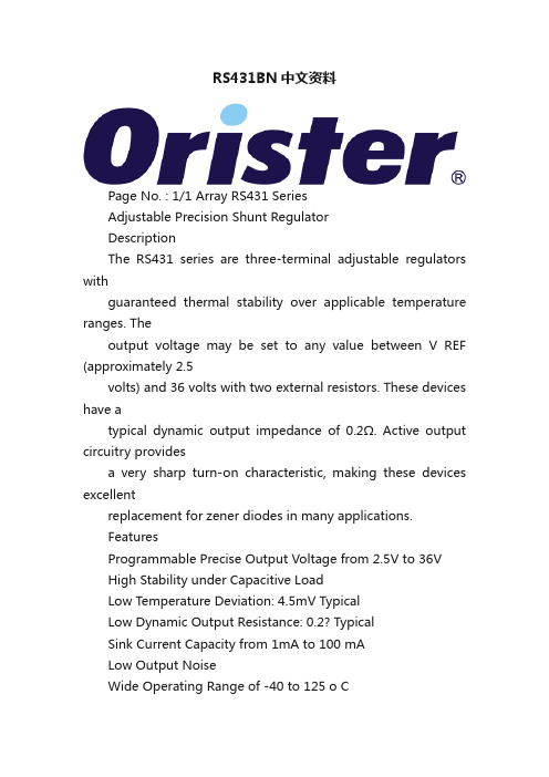
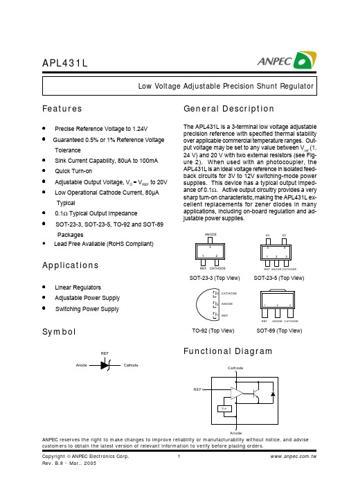
RS431BN中文资料Page No. : 1/1 Array RS431 SeriesAdjustable Precision Shunt RegulatorDescriptionThe RS431 series are three-terminal adjustable regulators withguaranteed thermal stability over applicable temperature ranges. Theoutput voltage may be set to any value between V REF (approximately 2.5volts) and 36 volts with two external resistors. These devices have atypical dynamic output impedance of 0.2Ω. Active output circuitry providesa very sharp turn-on characteristic, making these devices excellentreplacement for zener diodes in many applications.FeaturesProgrammable Precise Output Voltage from 2.5V to 36VHigh Stability under Capacitive LoadLow Temperature Deviation: 4.5mV TypicalLow Dynamic Output Resistance: 0.2? TypicalSink Current Capacity from 1mA to 100 mALow Output NoiseWide Operating Range of -40 to 125 o CLow Equivalent Full-range Temperature Coefficient with 20PPM/ o C TypicalAbsolute Maximum Ratings(Operating temperature range applies unless otherwise specified)Characteristics Symbol Value UnitCathode Voltage V KA 40 V Cathode Current Range (Continuous) I K -100~+150 mA Reference Input Current Range I REF 0.05~+10 mASOT-23 370TO-92 770mWPower Dissipation P D-- ---- --Operating Temperature Range (Max.) T opr -40~+125 *o C Storage Temperature Range T stg -65~+150 o COperating ConditionsCharacteristics Symbol Min. Max. UnitCathode Voltage V KA V REF 36 V Cathode Current Range (Continuous) I K 1 100 mAOperating Ambient Temperature Range -40 125 o CPage No. : 2/2Test Circuits=Functional Block Diagram=V REFFig 2. V IN V KTypical Performance CharacteristicsTypical Performance Characteristics (Continued)Typical Performance Characteristics (Continued)SOT-23 DimensionTO-92 DimensionOrdering InformationPackage V REF: 2.5±0.8% V REF: 2.5±0.4%RS431AN SOT-23 RS431BNTO-92 RS431BARS431AASoldering Methods for Orister’s Products1. Storage environment: Temperature=10o C~35o C Humidity=65%±15%2. Reflow soldering of surface-mount devicesProfile Feature Sn-Pb Eutectic Assembly Pb-Free AssemblyAverage ramp-up rate (T L to T P) <3o C/sec <3o C/sec Preheat - Temperature Min (Ts min) - Temperature Max (Ts max) - Time (min to max) (ts)100o C150o C60~120 sec150o C200o C60~180 secTsmax to T L- Ramp-up Rate <3o C/sec <3o C/sec Time maintained above:- Temperature (T L) - Time (t L)183o C60~150 sec217o C60~150 secPeak Temperature (T P) 240o C +0/-5o C 260o C +0/-5o C Time within 5o C of actual PeakTemperature (t P)10~30 sec 20~40 secRamp-down Rate <6o C/sec <6o C/secTime 25o C to Peak Temperature <6 minutes <8 minutes3. Flow (wave) soldering (solder dipping)Products Peak temperature Dipping timePb devices. 245o C ±5o C 5sec±1secPb-Free devices. 260o C +0/-5o C 5sec ±1secImportant Notice:All rights are reserved. Reproduction in whole or in part is prohibited without the prior written approval of Orister Corporation.Orister Corporation reserves the right to make changes to its products without notice.Orister Corporation products are not warranted to be suitable for use in Life-Support Applications, or systems.Orister Corporation assumes no liability for any consequence of customer product design, infringement of patents, or application assistance.。
IP431AC资料
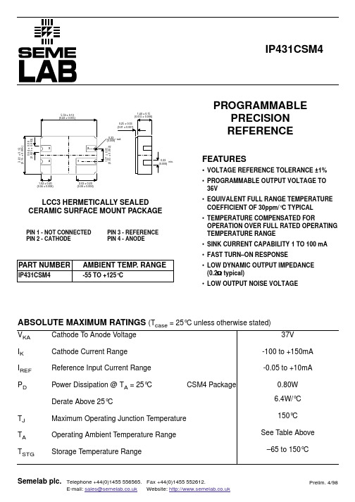
PROGRAMMABLEPRECISION REFERENCEV KA Cathode To Anode Voltage I K Cathode Current Range I REF Reference Input Current Range P DPower Dissipation @ T A = 25°C CSM4 PackageDerate Above 25°CT J Maximum Operating Junction Temperature T A Operating Ambient Temperature Range T STGStorage Temperature Range37V -100 to +150mA -0.05 to +10mA0.80W 6.4W/°C 150°C See Table Above –65 to 150°CABSOLUTE MAXIMUM RATINGS (T case = 25°C unless otherwise stated)FEATURES•VOLTAGE REFERENCE TOLERANCE ±1%•PROGRAMMABLE OUTPUT VOLTAGE TO 36V•EQUIVALENT FULL RANGE TEMPERATURE COEFFICIENT OF 30ppm/°C TYPICAL•TEMPERATURE COMPENSATED FOROPERATION OVER FULL RATED OPERATING TEMPERATURE RANGE•SINK CURRENT CAPABILITY 1 TO 100 mA •FAST TURN–ON RESPONSE•LOW DYNAMIC OUTPUT IMPEDANCE (0.2W typical)•LOW OUTPUT NOISE VOLTAGE5.59 ± 0.13(0.04 ± 0.008)(0.08 ± 0.008)1.40 ± 0.150.23min.3.81 ± 0.13PIN 1 - NOT CONNECTED PIN 2 - CATHODEPIN 3 - REFERENCE PIN 4 - ANODELCC3 HERMETICALLY SEALED CERAMIC SURFACE MOUNT PACKAGEBLOCK DIAGRAM DESCRIPTIONThe IP431A circuit is a monolithic three terminalprogrammable shunt regulator diode. The voltage reference operates as a low temperature coefficient zener which is programmable between V REF(2.5V) and 36 volts using two external resistors. The device has a wide operating current range of 1 mA to 100mA and a typical dynamic impedance of 0.2W. Active output circuitry provides a very sharp turn-on characteristic making these devices excellent replacements for zener diodes in manyapplications. Being a shunt regulator it can be used as either a positive or negative voltage reference.CATHODEANODEREFV KA Cathode To Anode Voltage I K Cathode Current Range V REF to 36V 1.0 to 100mARECOMMENDED OPERATING CONDITIONSR1|Z ka | »|Z ka | 1+R2NOTE 1The deviation parameter D V REF is defined as the differences between the maximum and minimum values obtained over the full operating ambient temperature range that applies.The average temperature coefficient of the reference input voltage,µV REF is defined as:µV REF can be positive or negative depending on whether µV REF Minor µV REF Max occurs at the lower ambient temperature.D V REF( )x 106ppm V REF @ 25°C µV REF = = °C D T A D V REF x 106=D T A (V REF @ 25°C)Example:D V REF = 8.0 mV and slope is positive,V REF @ 25°C = 2.495V, D T A = 70°C 0.008 x 106= 45.8 ppm/°CµV REF == 45.8 ppm/°C70 (2.495)NOTE 2The dynamic impedance Z ka is defined as:D VKA|Z ka | = D I KWhen the device is programmed with two external resistors, R1 and R2, (refer to Figure 2) the total dynamic impedance of the circuit is defined as:( )V REF =V REF Max -V REF MinT A = T2 - T1。
UTC431中文资料下载
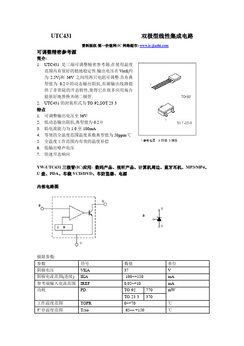
UTC431 双极型线性集成电路
资料版权:第一价值网(IC网络超市)
可调整精密参考源
简介:
1.UTC431是三端可调整精密参考源,在使用温度
范围内有很好的稳地稳定性.输出电压在Vref(约
为2.5V)和36V之间用两只电阻可调整.具有典
型值为0.2Ω的动态输出阻抗,有源输出线路提
供了非常陡的开态特性,使得它在很多应用场合
能很好地替换齐纳二极管.
2.UTC431的封装形式为TO-92,SOT-23-3
特点
1.可调整输出电压至36V
2.低动态输出阻抗,典型值为0.2Ω
3.陷电流能力为1.0至100mA
4.等效的全温度范围温度系数典型值为50ppm/℃
5.全温度工作范围内有效的温度补偿
6.低输出噪声电压
7.快速开态响应
YW-UTC431三极管(IC)应用: 数码产品、视听产品、计算机周边、蓝牙耳机、MP3/MP4、U盘、PDA、车载VCD/DVD、车防盜器、电源
内部电路图
极限参数:
注: T MIN=0℃,T MAX=+70℃*为应客户要求定制规格工作特性曲线
测试线路图
典型应用电路
封装外形图
产品信息:。
UC723 友顺UTC 电子元器件 芯片
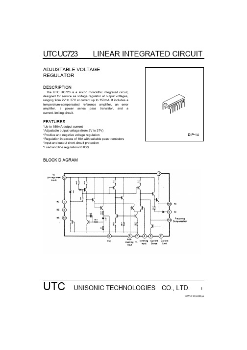
UTC UC723LINEAR INTEGRATED CIRCUITUTC UNISONIC TECHNOLOGIES CO., LTD.1QW-R103-006,AADJUSTABLE VOLTAGE REGULATORDESCRIPTIONThe UTC UC723 is a silicon monolithic integrated circuit, designed for service as voltage regulator at output voltages, ranging from 2V to 37V at current up to 150mA. It includes a temperature-compensated reference amplifier, an error amplifier, a power series pass transistor, and a current-limiting circuit.FEATURES*Up to 150mA output current*Adjustable output voltage (from 2V to 37V) *Positive and negative voltage regulation*Regulation in excess of 10A with suitable pass transistors *Input and output short-circuit protection *Load and line regulation< 0.03%BLOCK DIAGRAMUTC UC723LINEAR INTEGRATED CIRCUITUTC UNISONIC TECHNOLOGIES CO., LTD.2QW-R103-006,AABSOLUTE MAXIMUM RATINGS (Ta=25°C )PARAMETER SYMBOL VALUE UNITSupply Voltage(between V+ and V-) Vcc 40 VPulse Voltage for 50ms Vpulse 50 V Differential Input-Output VoltageVd40V Different Input Voltage (Between inverting and non-inverting inputs)Vid +-5 VDifferent Input Voltage (Between Non-inverting Input and V-) Vid 8 V Current from Zener Diode Terminal Iz 25 mA Power Dissipation Pd 900 mWOperating Temperature Topr -55 ~ 125 °C Storage TemperatureTstr-65 ~ 150°CELECTRICAL CHARACTERISTICS (Ta=25°C , V+=Vc=Vi=12V, Vo=5V, IL=1mA, C1=100Pf, Cref=0,Rscp=0, unless otherwise specified, divider impedance R1*R2/(R1+R2) at non-inverting input, terminal 5=10K Ω)PARAMETER SYMBOL TEST CONDITIONS MIN TYP MAX UNIT Quiescent Regulator Current ICCQ IL=0, VI=30V2.33.5 mA Input Voltage Range VI 9.5 40 V Output Voltage Range VO237VDifferential Input-Output VoltageVI-VO 3 38 VReference Voltage VREF6.957.15 7.35 V Line Regulation (note 1)∆VOVI=12V to 40VVI=12V to 15VVI=12V to 15V, Ta=-55~125°C0.02 0. 010. 20.1 %VoLoad Regulation (note 1) ∆VO IL=1mA TO 50mAIL=1mA TO 50mA,Ta=-55~125°C0.03 0. 15 0.6%VoOutput Voltage Temperature Coefficient∆VOTa=-55~125°C0.002 0.015%/°C Ripple Rejection (note 2)RRf=50Hz to 10KHz f=50Hz to 10KHz, Cref=5µFTmin<Ttyp<Tmax74 86 2.5dBShort Circuit Limiting Current ILIM Rscp=10Ω, Vo =0 65 mA Equivalent Noise RMS output Voltage (note 2)VNBW=100Hz to 10KHz, Cref=0 BW=100Hz to 10KHz, Cref=5µF-20 2.5µVNOTE 1: Line and load regulation specifications are given for conditions of a constant chip temperature. Forhigh dissipation condition, temperature drifts must be separately taken in account.NOTE 2: For Cref, see Fig. 1UTC UC723LINEAR INTEGRATED CIRCUITUTC UNISONIC TECHNOLOGIES CO., LTD.3QW-R103-006,AAPPLICATION CIRCUITUTC UC723LINEAR INTEGRATED CIRCUIT TYPICAL PERFORMANCE CHARACTERISTICSUTC UNISONIC TECHNOLOGIES CO., LTD. 4QW-R103-006,A。
YW-UTC431

可调整精密参考源
★UTC431是三端可调整精密参考源,在使用温度范围内有很 好的温度稳定性。输出电压在Vref(约为2.5V)和36V之间用 两只电阻可调整,具有典型值为0.2Ω的动态输出阻抗,有源 输出线路提供了非常陡的开态特性,使得它在很多应用场 合能很好地替换齐纳二极管。
★UTC431的封装形式为TO-92,SOT-23-3 。
2.445 2.495 2.545
4.5
17
mV
-1.0
-2.7 mV/V
-0.5
-2.0 mV/V
1.5
4
μA
0.4
1.2
μA
0.45
1.0
mA
0.05
1.0
μA
0.15
0.5
Ω
杭州友旺电子有限公司
2
2005.06.06 V1.1
UTC431
典型工作特性曲线
(mA)
(mV)
图 1 图图图图图图图图图图图
杭州友旺电子有限公司
3
2005.06.06 V1.1
UTC431
双极型线性集成电路
测试线路图
图7 VKA=VREF测试线路图 路图
输输
VKA
IKA
VREF
UTC431
典型应用线路
图10 并联稳压电源 源
Vi
Vo
R1
VREF R2 UTC431
Vo=(1+R1/R2)*V REF
图13 电流限制器或电流源
TA=全温度范围 VKA=VREF
VKA=36V,VREF=0 VKA=VREF,IKA=1—100mA
f≤1.0KHZ
最小值 典型值 最大值 单 位
UTCUC3843A中文资料
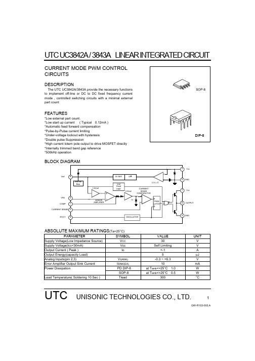
UTC UC3842A / 3843A LINEAR INTEGRATED CIRCUITUTC UNISONIC TECHNOLOGIES CO., LTD.1QW-R103-002,ACURRENT MODE PWM CONTROL CIRCUITSDESCRIPTIONThe UTC UC3842A/3843A provide the necessary functions to implement off-line or DC to DC fixed frequency current mode , controlled switching circuits with a minimal external part countFEATURES*Low external part count. *Low start up current ( Typical 0.12mA ) *Automatic feed forward compensation *Pulse-by-Pulse current limiting*Under-voltage lockout with hysteresis *Double pulse Suppression*High current totem pole output to drive MOSFET directly *Internally trimmed band gap reference *500kHz operationBLOCK DIAGRAMVref VFB COMPRT/CT VccOUTPUTVccABSOLUTE MAXIMUM RATINGS (Ta=25°C)PARAMETER SYMBOL VALUE UNITSupply Voltage(Low Impedance Source) V CC 30 VSupply Voltage(Icc<30mA) Vcc Self Limiting V Output Current ( Peak ) Io +-1 AOutput Energy(capacity Load) 5µJ Analog Inputs(pin 2,3) V I(ANA) -0.3 ~ +6.3 V Error Amplifier Output Sink Current I SINK(EA) 10 mAPower Dissipation PD DIP-8 at T amb <=25°C 1.0 W SOP-8 at T amb <=25°C 0.5 WLead Temperature( Soldering 10 Sec ) Tlead 300 °CUTC UC3842A / 3843A LINEAR INTEGRATED CIRCUITUTC UNISONIC TECHNOLOGIES CO., LTD.2QW-R103-002,A(continued)PARAMETRER SYMBOL VALUE UNITStorage Temperature Tstg -65 ~ +150°C Note 1: Ta>25°C, P D derated with 8mW/°C.ELECTRICAL CHARACTERISTICS (0°C <=Ta<=70°C,V CC =15V,R T =10k Ω,C T =3.3nF,unless otherwise specified)PARAMETER SYMBOL TEST CONDITIONS MIN TYP MAX UNITReference SectionOutput Voltage V REF Tj=25°C,Io=1mA 4.9 5 5.1 V Line Regulation ∆V REF 12<=V IN <=25V 6 20 mV Load Regulation ∆V REF1<=Io =20mA 6 25 mV Temperature Stability (Note 2) 0.2 0.4 mV/°CTotal Output Variation Line, Load, Temp(note 2) 4.82 5.18 V Output Noise Voltage Vosc 10Hz<=f<=10kHz,Tj=25°C (note 2) 50 uVLong Term Stability Ta=25°C,1000Hrs(note 2) 5 25 mV Output Short Circuit I SC -30-100 -180 mAOscillator Section Initial Accuracy f Tj=25°C 47 52 57 kHz Voltage Stability ∆f/∆Vcc 12<=Vcc<=25V 0.2 1 % Temperature Stability Tmin<=T A <=Tmax(note 2) 5 % Amplitude Vosc Vpin 4 peak to peak 1.7 VError Amplifier SectionInput Voltage V I(EA) Vpin 1=2.5V 2.42 2.50 2.58 V Input Bias Current I BIAS -0.3 -2 µA A VOL 2 <=Vo<=4V 60 90 dB Unity Gain Bandwidth Tj=25°C (note 2) 0.7 1 MHz PSRR I2<=Vcc<=25V 60 70 dB Output Sink Current Isink Vpin 2=2.7V,Vpin 1=1.1V 2 6 mA Output Source Current Isource Vpin 2=2.3V,Vpin 1=5V -0.5-0.8 mA Vout High V OH Vpin 2=2.3V, RL=15k Ω to GND 5 6 V Vout Low V OL Vpin 2=2.7V,Vpin 1=1.1V 0.7 1.1 VCurrent Sense sectionGain G V (note 3,4) 2.85 3 3.15 V/V Maximum Input signal V I(MAX)Vpin 1=5V( note 3) 0.9 1 1.1 V PSRR 12<=Vcc<=25V 70 dB Input Bias Current I BIAS -2 -10 µA Delay to Output Vpin 3=0 to 2V 150 300 nsOutput SectionOutput Low Level V OL Isink =20mA 0.1 0.4 VIsink =200mA 1.5 2.2 V Output High Level V OH Isource =20mA 13 13.5 V Isource =200mA 12 13.5 VRise Time t R Tj=25°C,C L =1nF(note 2)50 150 ns Fall Time t F Tj=25°C,C L =1nF(note 2)50 150 ns Under-Voltage Lockout Output SectionStart Threshold V TH(ST)UTC3842A 14.516 17.5 V UTC3843A 7.88.4 9 V Min. Operating Voltage V OPR(min)After Turn On UTC3842A8.510 11.5UTC3843A 7 7.6 8.2 VPWM SectionMaximum Duty Cycle D (MAX) 95 97 100 %UTC UC3842A / 3843A LINEAR INTEGRATED CIRCUITUTC UNISONIC TECHNOLOGIES CO., LTD.3QW-R103-002,APARAMETER SYMBOLTEST CONDITIONS MINTYP MAX UNITMinimum Duty CycleD (MIN)0 % Total Standby CurrentStart-up Current I ST 0.12 0.3 mAOperating Supply Current I CC(opr)Vpin 2=Vpin 3=0V 11 17 mA Vcc Zener Voltage Vz Icc=25mA 34 V note 2:These parameters, although guaranteed ,are not 100% tested in production. note 3:Parameters measured at trip point of latch with Vpin 2=0. note 4:Gain defined as:∆Vpin 1∆Vpin 3A=; 0<=Vpin3<=0.8Vnote 5:Adjust Vcc above the start threshold before setting at 15V.OPEN-LOOP LABORATORY TEST FIXTUREVrefVccAdjustHigh peak current associated with capacity loads necessitate careful grounding techniques. Timing and bypass capacitors should be connected close to pin 5 in single point GND. The transistor and 5k Ω potentio-meter are used to sample the oscillator waveform and apply an adjustable Ramp to Pin 3.UNDER-VOLTAGE LOCKOUTVonVoffVccDuring Under-Voltage Lockout, the output driver is biased to a high impedance state. Pin 6 should be shunt to GND with a bleeder resistor to prevent activating the power switch with output leakage currents.UTC UC3842A / 3843A LINEAR INTEGRATED CIRCUITUTC UNISONIC TECHNOLOGIES CO. LTD4QW-R103-002,AERROR AMPLIFIER CONFIGURATIONError amplifier can source or sink up to 0.5mACURRENT SENSE CIRCUITPeak current (Is) determined by the formula:Ismax=10V/Rs.A small RC filter be required to suppress switch transients.SLOPE COMPENSATIONA fraction of the oscillator ramp can be resistively summed with the current sense signal to provide slopecompensation for converts requiring duty cycles over 50%.Note that capacitor C, forms a filter with R2 to suppress the leading edge switch spikes.UTC UC3842A / 3843A LINEAR INTEGRATED CIRCUITUTC UNISONIC TECHNOLOGIES CO. LTD5QW-R103-002,AOSCILLATOR SECTIONLarge RT Small CTSmall RT Large CTV4V4INTERNAL CLOCKINTERNAL CLOCKDead time VS C T (R T >5k Ω) TimingResistance Vs Frequency 1101001101000.1td (µs)CT (nF)110RT (k ΩFrequency (Hz)SHUTDOWN TECHNIQUESShutdown UTC UC3842A can be accomplished by two methods; either raise pin 3 above 1V or pull Pin 1 below a voltage two diode drops above ground. Either method caused the output of PWM comparator to be high(refer to block diagram).The PWM latch is reset dominant so that the output will remain low until the next clock cycle after the shutdown condition at pins 1 and/or 3 is removed . In one example, an externally latched shut –down may be accomplished by adding an SCR which be reset by cycling Vcc below the lower UVLO threshold. At this point the reference turns off allowing the SCR to reset.UTC UC3842A / 3843A LINEAR INTEGRATED CIRCUITUTC UNISONIC TECHNOLOGIES CO. LTD6QW-R103-002,ATYPICAL PERFORMANCE CHARACTERISTICS0.010.1101234S a t u r a t i o n V o l t a g e (V )Output Current(Sourse or Sink Current) (A)7103106105104101021020406010080Frequency (Hz)V o l t a g e G a i n (d B )-180-135-90-45P H A S E (D e g r e e )Output Saturation Characteristics Error Amplifier Open-Loop Frequency ResponseUTC UC3842A / 3843A LINEAR INTEGRATED CIRCUITUTC UNISONIC TECHNOLOGIES CO. LTD7QW-R103-002,A-50-25255075100125150Vref (V)Temperature (°C)-50-250255075100125150I s t a r t (m A )Temperature (°C)-50-252550751001251509101112131415Icc (mA)Temperature (°C)Vref Temperature DriftIstart Temperature DriftIcc Temperature Drift。
IP431AI资料

PROGRAMMABLEPRECISION REFERENCEV KA Cathode To Anode Voltage I K Cathode Current Range I REF Reference Input Current Range P DPower Dissipation @ T A = 25°C CSM4 PackageDerate Above 25°CT J Maximum Operating Junction Temperature T A Operating Ambient Temperature Range T STGStorage Temperature Range37V -100 to +150mA -0.05 to +10mA0.80W 6.4W/°C 150°C See Table Above –65 to 150°CABSOLUTE MAXIMUM RATINGS (T case = 25°C unless otherwise stated)FEATURES•VOLTAGE REFERENCE TOLERANCE ±1%•PROGRAMMABLE OUTPUT VOLTAGE TO 36V•EQUIVALENT FULL RANGE TEMPERATURE COEFFICIENT OF 30ppm/°C TYPICAL•TEMPERATURE COMPENSATED FOROPERATION OVER FULL RATED OPERATING TEMPERATURE RANGE•SINK CURRENT CAPABILITY 1 TO 100 mA •FAST TURN–ON RESPONSE•LOW DYNAMIC OUTPUT IMPEDANCE (0.2W typical)•LOW OUTPUT NOISE VOLTAGE5.59 ± 0.13(0.04 ± 0.008)(0.08 ± 0.008)1.40 ± 0.150.23min.3.81 ± 0.13PIN 1 - NOT CONNECTED PIN 2 - CATHODEPIN 3 - REFERENCE PIN 4 - ANODELCC3 HERMETICALLY SEALED CERAMIC SURFACE MOUNT PACKAGEBLOCK DIAGRAM DESCRIPTIONThe IP431A circuit is a monolithic three terminalprogrammable shunt regulator diode. The voltage reference operates as a low temperature coefficient zener which is programmable between V REF(2.5V) and 36 volts using two external resistors. The device has a wide operating current range of 1 mA to 100mA and a typical dynamic impedance of 0.2W. Active output circuitry provides a very sharp turn-on characteristic making these devices excellent replacements for zener diodes in manyapplications. Being a shunt regulator it can be used as either a positive or negative voltage reference.CATHODEANODEREFV KA Cathode To Anode Voltage I K Cathode Current Range V REF to 36V 1.0 to 100mARECOMMENDED OPERATING CONDITIONSR1|Z ka | »|Z ka | 1+R2NOTE 1The deviation parameter D V REF is defined as the differences between the maximum and minimum values obtained over the full operating ambient temperature range that applies.The average temperature coefficient of the reference input voltage,µV REF is defined as:µV REF can be positive or negative depending on whether µV REF Minor µV REF Max occurs at the lower ambient temperature.D V REF( )x 106ppm V REF @ 25°C µV REF = = °C D T A D V REF x 106=D T A (V REF @ 25°C)Example:D V REF = 8.0 mV and slope is positive,V REF @ 25°C = 2.495V, D T A = 70°C 0.008 x 106= 45.8 ppm/°CµV REF == 45.8 ppm/°C70 (2.495)NOTE 2The dynamic impedance Z ka is defined as:D VKA|Z ka | = D I KWhen the device is programmed with two external resistors, R1 and R2, (refer to Figure 2) the total dynamic impedance of the circuit is defined as:( )V REF =V REF Max -V REF MinT A = T2 - T1。
TVR14431中文资料

Varistor Voltage
VlmA (V) 18 22 27 33 39 47 56 68 82 100 120 150 180 200 220 240 270 300 330 360 390 430 470
Max. Allowable Voltage
AC rms DC
(V)
(V)
11
14
14
Rua Juquiá, 217 - Vila Antonieta - S.B.C. - Cep:09629-040 - SP - Brasil Tel: (11) 4367-7411 - Fax: (11) 4367-7416 - .br - voltts@.br
Reference Capacitance
Dimensions
@1KHZ (pf) 1600 1500 1450 1400 1100 850 600 580 460 400 350 300 150 140 130 120 110 100 105 90 85 80 75
T(max.) (mm) 3.9 4.1 4.3 4.5 4.0 4.1 4.3 4.6 4.0 4.2 4.4 4.7 4.2 4.3 4.4 4.5 4.7 4.6 4.7 4.8 5.0 5.2 5.3
Ip 10/1000
(A)
(J)
2.5
0.9
2.5
1.1
2.5
1.4
2.5
1.7
2.5
2.1
2.5
2.5
2.5
3.1
2.5
3.6
10
5.5
10
6.5
10
7.8
10
9.7
10 11.7
10
LM431AIM3中文资料

LM431Adjustable Precision Zener Shunt RegulatorGeneral DescriptionThe LM431is a 3-terminal adjustable shunt regulator with guaranteed temperature stability over the entire temperature range of operation.It is now available in a chip sized pack-age (4-Bump micro SMD)using National’s micro SMD pack-age technology.The output voltage may be set at any level greater than 2.5V (V REF )up to 36V merely by selecting two external resistors that act as a voltage divided network.Due to the sharp turn-on characteristics this device is an excel-lent replacement for many zener diode applications.Featuresn Average temperature coefficient 50ppm/˚Cn Temperature compensated for operation over the full temperature rangen Programmable output voltage n Fast turn-on response n Low output noisen LM431in micro SMD packagen See AN-1112for micro SMD considerationsConnection DiagramsNote:*NC =Not internally connected.Must be electrically isolated from therest of the circuit for the microSMD package.TO-92:Plastic PackageDS010055-1Top ViewSO-8:8-Pin Surface MountDS010055-2Top viewSOT-23:3-Lead Small OutlineDS010055-28Top View 4-Bump micro SMDDS010055-54Top View(bump side down)March 2002LM431Adjustable Precision Zener Shunt Regulator©2002National Semiconductor Corporation Ordering InformationPackage Typical Accuracy Order Number/Package MarkingTemperature Range Transport MediaNSC Drawing0.5%1%2%TO-92LM431CCZ/LM431CCZ LM431BCZ/LM431BCZ LM431ACZ/LM431ACZ 0˚C to +70˚CRailsZ03ALM431CIZ/LM431CIZLM431BIZ/LM431BIZ LM431AIZ/LM431AIZ −40˚C to +85˚C SO-8LM431CCM/431CCM LM431BCM/431BCM LM431ACM/LM431ACM 0˚C to +70˚CRails and Tape &ReelM08A LM431CIM/431CIMLM431BIM/431BIM LM431AIM/LM431AIM −40˚C to +85˚C SOT-23LM431CCM3/N1B LM431BCM3/N1D LM431ACM3/N1F 0˚C to +70˚CRails and Tape &ReelMF03A LM431CIM3N1ALM431BIM3N1CLM431AIM3N1E−40˚C to +85˚C micro SMD––LM431AIBPLM431AIBPX(Note 1)−40˚C to +85˚C250Units Tape and Reel3k Units Tape and ReelBPA04AFBNote 1:The micro SMD package marking is a 1digit manufacturing Date Code onlymicro SMD Top View Marking ExampleDS010055-56L M 431 2Symbol and Functional DiagramsDC Test CircuitsDS010055-99DS010055-55DS010055-4FIGURE 1.Test Circuit for V Z =V REFDS010055-5Note:V Z =V REF (1+R1/R2)+I REF •R1FIGURE 2.Test Circuit for V Z >V REFDS010055-6FIGURE 3.Test Circuit for Off-State CurrentLM4313Absolute Maximum Ratings (Note 2)If Military/Aerospace specified devices are required,please contact the National Semiconductor Sales Office/Distributors for availability and specifications.Storage Temperature Range −65˚C to +150˚C Operating Temperature Range Industrial (LM431xI)−40˚C to +85˚C Commercial (LM431xC)0˚C to +70˚C Soldering InformationInfrared or Convection (20sec.)235˚CWave Soldering (10sec.)260˚C (lead temp.)Cathode Voltage37VContinuous Cathode Current−10mA to +150mAReference Voltage−0.5V Reference Input Current10mA Internal Power Dissipation (Notes 3,4)TO-92Package SO-8Package SOT-23Package 0.78W 0.81W 0.28W micro SMD Package0.30WOperating ConditionsMin Max Cathode Voltage V REF 37V Cathode Current1.0mA100mALM431Electrical CharacteristicsT A =25˚C unless otherwise specified Symbol ParameterConditionsMin Typ Max Units V REFReference VoltageV Z =V REF ,I I =10mA 2.4402.4952.550VLM431A (Figure 1)V Z =V REF ,I I =10mA 2.4702.4952.520VLM431B (Figure 1)V Z =V REF ,I I =10mA 2.4852.5002.510VLM431C (Figure 1)V DEVDeviation of Reference Input Voltage Over V Z =V REF ,I I =10mA,8.017mVTemperature (Note 5)T A =Full Range (Figure 1)Ratio of the Change in Reference Voltage I Z =10mAV Z from V REF to 10V −1.4−2.7mV/Vto the Change in Cathode Voltage(Figure 2)V Z from 10V to 36V−1.0−2.0I REF Reference Input CurrentR 1=10k Ω,R 2=∞, 2.04.0µA I I =10mA (Figure 2)∝I REFDeviation of Reference Input Current over R 1=10k Ω,R 2=∞,TemperatureI I =10mA,0.4 1.2µA T A =Full Range (Figure 2)I Z(MIN)Minimum Cathode Current for Regulation V Z =V REF (Figure 1)0.4 1.0mA I Z(OFF)Off-State CurrentV Z =36V,V REF =0V (Figure 3)0.31.0µA r ZDynamic Output Impedance (Note 6)V Z =V REF ,LM431A,0.75ΩFrequency =0Hz (Figure 1)V Z =V REF ,LM431B,LM431C 0.50ΩFrequency =0Hz (Figure 1)Note 2:Absolute Maximum Ratings indicate limits beyond which damage to the device may occur.Electrical specifications do not apply when operating the device beyond its rated operating conditions.Note 3:T J Max =150˚C.Note 4:Ratings apply to ambient temperature at 25˚C.Above this temperature,derate the TO-92at 6.2mW/˚C,the SO-8at 6.5mW/˚C,the SOT-23at 2.2mW/˚C and the micro SMD at 3mW/˚C.Note 5:Deviation of reference input voltage,V DEV ,is defined as the maximum variation of the reference input voltage over the full temperature range.L M 431 4LM431Electrical Characteristics(Continued)Where:T 2−T 1=full temperature change (0-70˚C).∝V REF can be positive or negative depending on whether the slope is positive or negative.Example:V DEV =8.0mV,V REF =2495mV,T 2−T 1=70˚C,slope is positive.Note 6:The dynamic output impedance,r Z ,is defined as:When the device is programmed with two external resistors,R1and R2,(see Figure 2),the dynamic output impedance of the overall circuit,r Z ,is defined as:Equivalent CircuitDS010055-7The average temperature coefficient of the reference input voltage,∝V REF ,is defined as:DS010055-3LM4315Typical Performance CharacteristicsInput Current vs V ZDS010055-29Thermal InformationDS010055-30Input Current vs V ZDS010055-31Dynamic Impedance vs FrequencyDS010055-9DS010055-10Stability Boundary ConditionsDS010055-11Note:The areas under the curves represent conditions that may cause the device to oscillate.For curves B,C,and D,R2and V +were adjusted to establish the initial V Z and I Z conditions with C L =0.V +and C L were then adjusted to determine the ranges of stability.Test Circuit for Curve A Above DS010055-12Test Circuit for Curves B,C and D AboveDS010055-13L M 431 6Typical ApplicationsShunt RegulatorDS010055-14Single Supply Comparator withTemperature Compensated ThresholdDS010055-15Series RegulatorDS010055-16Output Control of a ThreeTerminal Fixed RegulatorDS010055-17Higher Current Shunt RegulatorDS010055-18Crow BarDS010055-19LM4317Typical Applications(Continued)Over Voltage/Under VoltageProtection CircuitDS010055-20Voltage MonitorDS010055-21L M 431 8Typical Applications(Continued)Application Info1.0MountingTo ensure that the geometry of the micro SMD packagemaintains good physical contact with the printed circuitboard,pin A1(NC)must be soldered to the pcb.Please seeAN-1112for more detailed information regarding boardmounting techniques for the micro SMD package.2.0LM431micro SMD Light SensitivityWhen the LM431micro SMD package is exposed to brightsunlight,normal office fluorescent light,and other LED’s andlasers,it operates within the guaranteed limits specified inthe electrical characteristics table.Delay TimerDS010055-22Current Limiter or Current SourceDS010055-23Constant Current SinkDS010055-24LM4319Physical Dimensionsinches (millimeters)unless otherwise notedNS Package Number M08ASOT-23Molded Small Outline Transistor Package (M3)NS Package Number MF03AL M 431 10LM431 Physical Dimensions inches(millimeters)unless otherwise noted(Continued)11Physical Dimensions inches(millimeters)unless otherwise noted(Continued)LIFE SUPPORT POLICYNATIONAL’S PRODUCTS ARE NOT AUTHORIZED FOR USE AS CRITICAL COMPONENTS IN LIFE SUPPORT DEVICES OR SYSTEMS WITHOUT THE EXPRESS WRITTEN APPROVAL OF THE PRESIDENT AND GENERAL COUNSEL OF NATIONAL SEMICONDUCTOR CORPORATION.As used herein:1.Life support devices or systems are devices orsystems which,(a)are intended for surgical implantinto the body,or(b)support or sustain life,andwhose failure to perform when properly used inaccordance with instructions for use provided in thelabeling,can be reasonably expected to result in asignificant injury to the user.2.A critical component is any component of a lifesupport device or system whose failure to performcan be reasonably expected to cause the failure ofthe life support device or system,or to affect itssafety or effectiveness.National SemiconductorCorporationAmericasEmail:support@National SemiconductorEuropeFax:+49(0)180-5308586Email:europe.support@Deutsch Tel:+49(0)6995086208English Tel:+44(0)8702402171Français Tel:+33(0)141918790National SemiconductorAsia Pacific CustomerResponse GroupTel:65-2544466Fax:65-2504466Email:ap.support@National SemiconductorJapan Ltd.Tel:81-3-5639-7560Fax:81-3-5639-7507 NOTES:UNLESS OTHERWISE SPECIFIED1.EPOXY COATING2.63Sn/37Pb EUTECTIC BUMP3.RECOMMEND NON-SOLDER MASK DEFINED LANDING PAD.4.PIN A1IS ESTABLISHED BY LOWER LEFT CORNER WITH RESPECT TO TEXT ORIENTATION.REMAINING PINS ARENUMBERED.5.XXX IN DRAWING NUMBER REPRESENTS PACKAGE SIZE VARIATION WHERE X1IS PACKAGE WIDTH,X2ISPACKAGE LENGTH AND X3IS PACKAGE HEIGHT.6.REFERENCE JEDEC REGISTRATION MO-211,VARIATION BA.4-Bump micro SMDX1=0.777X2=0.904X3=0.850NS Package Number BPA04AFBLM431AdjustablePrecisionZenerShuntRegulatorNational does not assume any responsibility for use of any circuitry described,no circuit patent licenses are implied and National reserves the right at any time without notice to change said circuitry and specifications.。
UTC报警培训技术培训手册

UTC(interlogix) 报警产品技术手册二零一四年七月陕西鹰威科技有限公VERSION1.0第 2 页第 3 页前言第 4 页前言本手册是为了培养合格的UTC 报警产品工程人员与销售人员而编写。
本手册重点介绍防盗系统原理以及UTC 各种防盗产品的特点及其应用方法,使得销售人员在给客户作配置方案时做到合理、有效,工程技术人员在做技术方案时能有的放矢、合理布局。
同时,还将介绍一些应用经验和故障排除方法,给技术人员维修UTC 产品提供参考。
最后,还会举一些应用实例帮助理解。
本手册将分为五大部分:第一部分介绍防盗系统基本构成与每一部分的原理,是防盗报警的入门篇。
第二部分介绍UTC 的防盗产品,深入了解UTC 报警产品原理到每个产品的特点。
第三部分阐述如何选择配置一个防盗系统,以及在工程设计、安装时的注意事项。
第四部分介绍常见故障的排除方法。
第五部分列举一些常用主机的一般使用方法,并配合实际应用例子,一步一步地学习安装、编程方法。
防盗报警系统构成与操作──用户端报警系统第 5 页1. 防盗报警系统构成与操作什么是防盗报警系统?是不是防盗门、防盗网之类?这是许多人对防盗报警的第一个反应,而我们这里所指的防盗系统,是完全不同的一个概念,是利用电子设备去达到自动防盗功能的先进的电子防盗系统。
为了从完整的概念去理解报警系统,本章我们将介绍报警系统的基本结构,为了理解报警系统的工作原理,我们还将介绍防盗报警系统的基本操作方法。
在学习本章时,我们要留意以下几个问题: 一个完整的防盗报警系统是由几部分构成的?⋯⋯ 各个组成部分在系统中的作用是什么?⋯⋯防盗系统是如何运作的?是如何在无人值守的情况下去实现防盗的目的?⋯⋯1.1 防盗系统构成我们这里所指的防盗系统是电子防盗报警系统,是在无人值守的地方,通过电子探测技术判断非法入侵行为,然后自动在现场发出警报,并同时自动将警情传送到专门处理警情的报警中心。
LM431中文手册
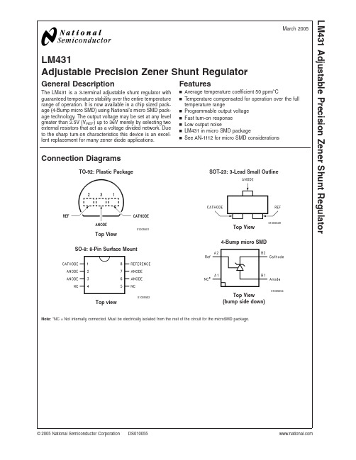
LM431Adjustable Precision Zener Shunt RegulatorGeneral DescriptionThe LM431is a 3-terminal adjustable shunt regulator with guaranteed temperature stability over the entire temperature range of operation.It is now available in a chip sized pack-age (4-Bump micro SMD)using National’s micro SMD pack-age technology.The output voltage may be set at any level greater than 2.5V (V REF )up to 36V merely by selecting two external resistors that act as a voltage divided network.Due to the sharp turn-on characteristics this device is an excel-lent replacement for many zener diode applications.Featuresn Average temperature coefficient 50ppm/˚Cn Temperature compensated for operation over the full temperature rangen Programmable output voltage n Fast turn-on response n Low output noisen LM431in micro SMD packagen See AN-1112for micro SMD considerationsConnection DiagramsTO-92:Plastic Package01005501Top ViewSO-8:8-Pin Surface Mount01005502Top viewSOT-23:3-Lead Small Outline01005528Top View 4-Bump micro SMD01005554Top View(bump side down)Note:*NC =Not internally connected.Must be electrically isolated from the rest of the circuit for the microSMD package.March 2005LM431Adjustable Precision Zener Shunt Regulator©2005National Semiconductor Corporation Ordering InformationPackageTypical Accuracy Order Number/PackageMarking TemperatureRangeTransport MediaNSC Drawing0.5%1%2%TO-92LM431CCZ/LM431CCZ LM431BCZ/LM431BCZ LM431ACZ/LM431ACZ 0˚C to +70˚CRailsZ03ALM431CIZ/LM431CIZLM431BIZ/LM431BIZ LM431AIZ/LM431AIZ −40˚C to +85˚CSO-8LM431CCM/431CCM LM431BCM/431BCMLM431ACM/LM431ACM0˚C to +70˚CRailsM08ALM431CCMX/431CCM LM431BCMX/431BCM LM431ACMX/LM431ACM Tape &ReelLM431CIM/431CIM LM431BIM/431BIM LM431AIM/LM431AIM −40˚C to +85˚CRailsLM431CIMX/431CIMLM431BIMX/431BIMLM431AIMX/LM431AIMTape &ReelSOT-23LM431CCM3/N1BLM431BCM3/N1D LM431ACM3/N1F0˚C to +70˚CRailsMF03ALM431CCM3X/N1B LM431BCM3X/N1D LM431ACM3X/N1F Tape &ReelLM431CIM3N1ALM431BIM3N1CLM431AIM3N1E−40˚C to +85˚CRailsLM431CIM3XN1ALM431BIM3X N1C LM431AIM3XN1ETape &Reel micro SMD––LM431AIBPLM431AIBPX (Note 1)−40˚C to +85˚C 250Units Tape andReel3k Units Tape andReelBPA04AFBNote 1:The micro SMD package marking is a 1digit manufacturing Date Code onlymicro SMD Top View Marking Example01005556L M 431 2Symbol and Functional Diagrams0100559901005555DC Test Circuits01005506Test Circuit for Off-State Current01005504FIGURE 1.Test Circuit for V Z =V REF01005505Note:V Z =V REF (1+R1/R2)+I REF •R1FIGURE 2.Test Circuit for V Z >V REFLM4313Absolute Maximum Ratings (Note 2)If Military/Aerospace specified devices are required,please contact the National Semiconductor Sales Office/Distributors for availability and specifications.Storage Temperature Range −65˚C to +150˚COperating Temperature Range Industrial (LM431xI)−40˚C to +85˚C Commercial (LM431xC)0˚C to +70˚C Soldering InformationInfrared or Convection (20sec.)235˚CWave Soldering (10sec.)260˚C (lead temp.)Cathode Voltage37VContinuous Cathode Current−10mA to +150mA Reference Voltage −0.5V Reference Input Current10mAInternal Power Dissipation (Notes 3,4)TO-92Package SO-8Package SOT-23Package 0.78W 0.81W 0.28W micro SMD Package0.30WOperating ConditionsMinMax Cathode Voltage V REF 37V Cathode Current1.0mA100mALM431Electrical CharacteristicsT A =25˚C unless otherwise specified Symbol ParameterConditionsMin Typ Max Units V REFReference VoltageV Z =V REF ,I I =10mA 2.4402.4952.550VLM431A (Figure 1)V Z =V REF ,I I =10mA 2.4702.4952.520VLM431B (Figure 1)V Z =V REF ,I I =10mA 2.4852.5002.510VLM431C (Figure 1)V DEVDeviation of Reference Input Voltage Over V Z =V REF ,I I =10mA,8.017mVTemperature (Note 5)T A =Full Range (Figure 1)Ratio of the Change in Reference Voltage I Z =10mA V Z from V REF to 10V −1.4−2.7mV/Vto the Change in Cathode Voltage(Figure 2)V Z from 10V to 36V−1.0−2.0I REF Reference Input CurrentR 1=10k Ω,R 2=∞, 2.04.0µA I I =10mA (Figure 2)∝I REFDeviation of Reference Input Current over R 1=10k Ω,R 2=∞,TemperatureI I =10mA,0.4 1.2µA T A =Full Range (Figure 2)I Z(MIN)Minimum Cathode Current for Regulation V Z =V REF (Figure 1)0.4 1.0mA I Z(OFF)Off-State CurrentV Z =36V,V REF =0V (Figure *NO TARGET FOR fi*)0.31.0µA r ZDynamic Output Impedance (Note 6)V Z =V REF ,LM431A,0.75ΩFrequency =0Hz (Figure 1)V Z =V REF ,LM431B,LM431C 0.50ΩFrequency =0Hz (Figure 1)Note 2:Absolute Maximum Ratings indicate limits beyond which damage to the device may occur.Electrical specifications do not apply when operating the device beyond its rated operating conditions.Note 3:T J Max =150˚C.Note 4:Ratings apply to ambient temperature at 25˚C.Above this temperature,derate the TO-92at 6.2mW/˚C,the SO-8at 6.5mW/˚C,the SOT-23at 2.2mW/˚C and the micro SMD at 3mW/˚C.Note 5:Deviation of reference input voltage,V DEV ,is defined as the maximum variation of the reference input voltage over the full temperature range.L M 431 4LM431Electrical Characteristics(Continued)01005507The average temperature coefficient of the reference input voltage,∝V REF ,is defined as:Where:T 2−T 1=full temperature change (0-70˚C).∝V REF can be positive or negative depending on whether the slope is positive or negative.Example:V DEV =8.0mV,V REF =2495mV,T 2−T 1=70˚C,slope is positive.Note 6:The dynamic output impedance,r Z ,is defined as:When the device is programmed with two external resistors,R1and R2,(see Figure 2),the dynamic output impedance of the overall circuit,r Z ,is defined as:LM4315Equivalent Circuit01005503Typical Performance CharacteristicsInput Current vs V ZThermal Information0100552901005530Input Current vs V ZDynamic Impedance vs Frequency0100553101005509L M 431 6Typical Performance Characteristics(Continued)Stability Boundary Conditions01005511Note:The areas under the curves represent conditions that may cause thedevice to oscillate.For curves B,C,and D,R2and V+were adjusted toestablish the initial V Z and I Z conditions with C L=0.V+and C L were thenadjusted to determine the ranges of stability.01005510Test Circuit for Curve A Above Test Circuit for Curves B,C and D Above0100551201005513Typical ApplicationsShunt Regulator01005514Single Supply Comparator withTemperature Compensated Threshold01005515LM4317Typical Applications(Continued)Series Regulator01005516Output Control of a ThreeTerminal Fixed Regulator01005517Higher Current Shunt Regulator01005518Crow Bar01005519 LM4318Typical Applications(Continued)Over Voltage/Under VoltageProtection Circuit01005520Voltage Monitor01005521LM4319Typical Applications(Continued)Delay Timer01005522Current Limiter or Current Source01005523Constant Current Sink01005524Application Info1.0MountingTo ensure that the geometry of the micro SMD packagemaintains good physical contact with the printed circuitboard,pin A1(NC)must be soldered to the pcb.Please seeAN-1112for more detailed information regarding boardmounting techniques for the micro SMD package.2.0LM431micro SMD Light SensitivityWhen the LM431micro SMD package is exposed to brightsunlight,normal office fluorescent light,and other LED’s andlasers,it operates within the guaranteed limits specified inthe electrical characteristics table.LM43110Physical Dimensionsinches (millimeters)unless otherwise noted8-Pin SOICNS Package Number M08ASOT-23Molded Small Outline Transistor Package (M3)NS Package Number MF03ALM43111Physical Dimensionsinches (millimeters)unless otherwise noted (Continued)NS Package Number Z03AL M 431 12Physical Dimensionsinches (millimeters)unless otherwise noted (Continued)NOTES:UNLESS OTHERWISE SPECIFIED 1.EPOXY COATING2.63Sn/37Pb EUTECTIC BUMP3.RECOMMEND NON-SOLDER MASK DEFINED LANDING PAD.4.PIN A1IS ESTABLISHED BY LOWER LEFT CORNER WITH RESPECT TO TEXT ORIENTATION.REMAINING PINS ARE NUMBERED.5.XXX IN DRAWING NUMBER REPRESENTS PACKAGE SIZE VARIATION WHERE X1IS PACKAGE WIDTH,X2IS PACKAGE LENGTH AND X3IS PACKAGE HEIGHT.6.REFERENCE JEDEC REGISTRATION MO-211,VARIATION BA.4-Bump micro SMDX1=0.777X2=0.904X3=0.850NS Package Number BPA04AFBNational does not assume any responsibility for use of any circuitry described,no circuit patent licenses are implied and National reserves the right at any time without notice to change said circuitry and specifications.For the most current product information visit us at .LIFE SUPPORT POLICYNATIONAL’S PRODUCTS ARE NOT AUTHORIZED FOR USE AS CRITICAL COMPONENTS IN LIFE SUPPORT DEVICES OR SYSTEMS WITHOUT THE EXPRESS WRITTEN APPROVAL OF THE PRESIDENT AND GENERAL COUNSEL OF NATIONAL SEMICONDUCTOR CORPORATION.As used herein:1.Life support devices or systems are devices or systems which,(a)are intended for surgical implant into the body,or (b)support or sustain life,and whose failure to perform when properly used in accordance with instructions for use provided in the labeling,can be reasonably expected to result in a significant injury to the user.2.A critical component is any component of a life support device or system whose failure to perform can be reasonably expected to cause the failure of the life support device or system,or to affect its safety or effectiveness.BANNED SUBSTANCE COMPLIANCENational Semiconductor manufactures products and uses packing materials that meet the provisions of the Customer Products Stewardship Specification (CSP-9-111C2)and the Banned Substances and Materials of Interest Specification (CSP-9-111S2)and contain no ‘‘Banned Substances’’as defined in CSP-9-111S2.National Semiconductor Americas Customer Support CenterEmail:new.feedback@ Tel:1-800-272-9959National SemiconductorEurope Customer Support CenterFax:+49(0)180-5308586Email:europe.support@Deutsch Tel:+49(0)6995086208English Tel:+44(0)8702402171Français Tel:+33(0)141918790National Semiconductor Asia Pacific Customer Support CenterEmail:ap.support@National SemiconductorJapan Customer Support Center Fax:81-3-5639-7507Email:jpn.feedback@ Tel:81-3-5639-7560LM431Adjustable Precision Zener Shunt Regulator。
UTC386中文PDF资料
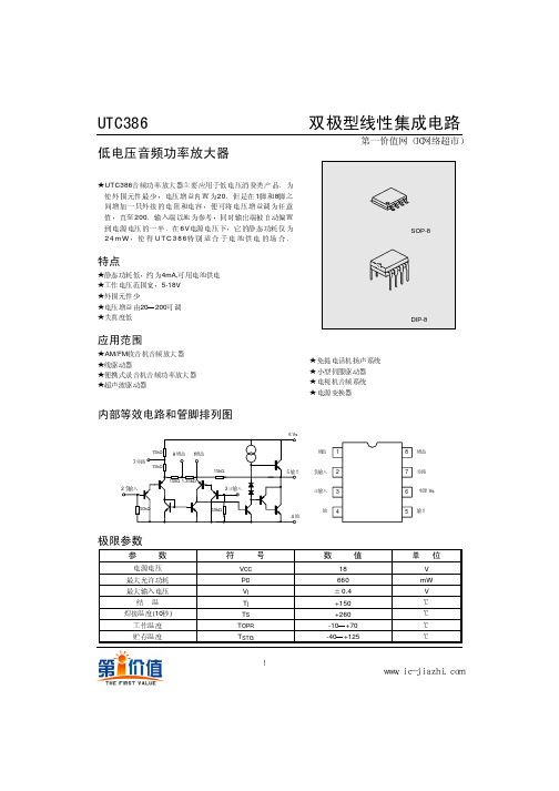
Vs=12V Vs=9V
THD=10% THD=3%
Vs=6V
0.2
0.4
0.6
输输输输 (W)
0.8
1.0
图 10 图图图图图图图图
27
26
25
24
23
电电电电
22 21
20
19
18
17
101
102
103
10 4
105
频输 (Hz)
图 12 图图图图图 =200
Vs
6
10μF
2
1 8
250μF
Vin
在一些特殊的应用中,也可平行于内部负反馈电阻外接阻容元件来进行增益和频响调整。例如,我们可以通过 提升负反馈频响网络以补偿扬声器低频段灵敏度低的缺点,它可以通过在1脚和5脚之间(平行于内部15KΩ电阻)接一 个RC串联网络来实现。对于6dB的有效低频提升来说:R≈15KΩ,当8脚开路时,能保证稳定工作的R最小值为 R=10KΩ,如果1脚和8脚之间有旁路电容,则R的最小值降为R=2KΩ,有这项限制的原因为放大器内部补偿仅至闭
符号
VCC PD VI Tj TS TOPR TSTG
数值
18 660
±0.4
+150 +260
— -10 +70 — -40 +125
单位
V mW
V
℃ ℃ ℃ ℃
1 www.ic-jiazhi.com
UTC386
双极型线性集成电路
℃ 电参数(TA=25 )
第一价值网(IC网络超市)
参
数 符号
测试条件
UTC386
5
3
10kΩ
4
UTCUC3842A中文资料

UTCUC3842A中⽂资料UTC UC3842A / 3843A LINEAR INTEGRATED CIRCUITUTC UNISONIC TECHNOLOGIES CO., LTD.1QW-R103-002,ACURRENT MODE PWM CONTROL CIRCUITSDESCRIPTIONThe UTC UC3842A/3843A provide the necessary functions to implement off-line or DC to DC fixed frequency current mode , controlled switching circuits with a minimal external part countFEATURES*Low external part count. *Low start up current ( Typical 0.12mA ) *Automatic feed forward compensation *Pulse-by-Pulse current limiting*Under-voltage lockout with hysteresis *Double pulse Suppression*High current totem pole output to drive MOSFET directly *Internally trimmed band gap reference *500kHz operation BLOCK DIAGRAMVref VFB COMPRT/CT VccOUTPUTVccABSOLUTE MAXIMUM RATINGS (Ta=25°C)PARAMETER SYMBOL VALUE UNITSupply Voltage(Low Impedance Source) V CC 30 VSupply Voltage(Icc<30mA) Vcc Self Limiting V Output Current ( Peak ) Io +-1 AOutput Energy(capacity Load) 5µJ Analog Inputs(pin 2,3) V I(ANA) -0.3 ~ +6.3 V Error Amplifier Output Sink Current I SINK(EA) 10 mAPower Dissipation PD DIP-8 at T amb <=25°C 1.0 W SOP-8 at T amb <=25°C 0.5 WLead Temperature( Soldering 10 Sec ) Tlead 300 °CUTC UC3842A / 3843A LINEAR INTEGRATED CIRCUITUTC UNISONIC TECHNOLOGIES CO., LTD.2QW-R103-002,A(continued)PARAMETRER SYMBOL VALUE UNITStorage Temperature Tstg -65 ~ +150°C Note 1: Ta>25°C, P D derated with 8mW/°C.ELECTRICAL CHARACTERISTICS (0°C <=Ta<=70°C,V CC =15V,R T =10k ?,C T =3.3nF,unless otherwise specified) PARAMETER SYMBOL TEST CONDITIONS MIN TYP MAX UNITReference SectionOutput Voltage V REF Tj=25°C,Io=1mA 4.9 5 5.1 V Line Regulation ?V REF 12<=V IN <=25V 6 20 mV Load Regulation ?V REF1<=Io =20mA 6 25 mV Temperature Stability (Note 2) 0.2 0.4 mV/°CTotal Output Variation Line, Load, Temp(note 2) 4.82 5.18 V Output Noise Voltage Vosc 10Hz<=f<=10kHz,Tj=25°C (note 2) 50 uVLong Term Stability Ta=25°C,1000Hrs(note 2) 5 25 mV Output Short Circuit I SC -30-100 -180 mAOscillator Section Initial Accuracy f Tj=25°C 47 52 57 kHz Voltage Stability ?f/?Vcc 12<=Vcc<=25V 0.2 1 % Temperature Stability Tmin<=T A <=Tmax(note 2) 5 % Amplitude Vosc Vpin 4 peak to peak 1.7 VError Amplifier SectionInput Voltage V I(EA) Vpin 1=2.5V 2.42 2.50 2.58 V Input Bias Current I BIAS -0.3 -2 µA A VOL 2 <=Vo<=4V 60 90 dB Unity Gain Bandwidth Tj=25°C (note 2) 0.7 1 MHz PSRR I2<=Vcc<=25V 60 70 dB Output Sink Current Isink Vpin 2=2.7V,Vpin 1=1.1V 2 6 mA Output Source Current Isource Vpin 2=2.3V,Vpin 1=5V -0.5-0.8 mA Vout High V OH Vpin 2=2.3V, RL=15k ? to GND 5 6 V Vout Low V OL Vpin 2=2.7V,Vpin 1=1.1V 0.7 1.1 VCurrent Sense sectionGain G V (note 3,4) 2.85 3 3.15 V/V Maximum Input signal V I(MAX)Vpin 1=5V( note 3) 0.9 1 1.1 V PSRR 12<=Vcc<=25V 70 dB Input Bias Current I BIAS -2 -10 µA Delay to Output Vpin 3=0 to 2V 150 300 nsOutput SectionOutput Low Level V OL Isink =20mA 0.1 0.4 VIsink =200mA 1.5 2.2 V Output High Level V OH Isource =20mA 13 13.5 V Isource =200mA 12 13.5 VRise Time t R Tj=25°C,C L =1nF(note 2)50 150 ns Fall Time t F Tj=25°C,C L =1nF(note 2)50 150 ns Under-Voltage Lockout Output SectionStart Threshold V TH(ST)UTC3842A 14.516 17.5 V UTC3843A 7.88.4 9 V Min. Operating Voltage V OPR(min)After Turn On UTC3842A8.510 11.5UTC3843A 7 7.6 8.2 VPWM SectionMaximum Duty Cycle D (MAX) 95 97 100 %UTC UC3842A / 3843A LINEAR INTEGRATED CIRCUITUTC UNISONIC TECHNOLOGIES CO., LTD.3QW-R103-002,APARAMETER SYMBOLTEST CONDITIONS MINTYP MAX UNITMinimum Duty CycleD (MIN)0 % Total Standby CurrentStart-up Current I ST 0.12 0.3 mAOperating Supply Current I CC(opr)Vpin 2=Vpin 3=0V 11 17 mA Vcc Zener Voltage Vz Icc=25mA 34 V note 2:These parameters, although guaranteed ,are not 100% tested in production. note 3:Parameters measured at trip point of latch with Vpin 2=0. note 4:Gain defined as:Vpin 1Vpin 3A=; 0<=Vpin3<=0.8Vnote 5:Adjust Vcc above the start threshold before setting at 15V.OPEN-LOOP LABORATORY TEST FIXTUREVrefVccAdjustHigh peak current associated with capacity loads necessitate careful grounding techniques. Timing and bypass capacitors should be connected close to pin 5 in single point GND. The transistor and 5k ? potentio-meter are used to sample the oscillator waveform and apply an adjustable Ramp to Pin 3.UNDER-VOLTAGE LOCKOUTVonVoffVccDuring Under-Voltage Lockout, the output driver is biased to a high impedance state. Pin 6 should be shunt to GND with a bleeder resistor to prevent activating the power switch with output leakage currents.UTC UC3842A / 3843A LINEAR INTEGRATED CIRCUITUTC UNISONIC TECHNOLOGIES CO. LTD4QW-R103-002,AERROR AMPLIFIER CONFIGURATIONError amplifier can source or sink up to 0.5mACURRENT SENSE CIRCUITPeak current (Is) determined by the formula:Ismax=10V/Rs.A small RC filter be required to suppress switch transients.SLOPE COMPENSATIONA fraction of the oscillator ramp can be resistively summed with the current sense signal to provide slope compensation for converts requiring duty cycles over 50%.Note that capacitor C, forms a filter with R2 to suppress the leading edge switch spikes.UTC UC3842A / 3843A LINEAR INTEGRATED CIRCUITUTC UNISONIC TECHNOLOGIES CO. LTD5QW-R103-002,AOSCILLATOR SECTIONLarge RT Small CTSmall RT Large CTV4V4INTERNAL CLOCKINTERNAL CLOCKDead time VS C T (R T >5k ?) TimingResistance Vs Frequency 1101001101000.1td (µs)CT (nF)110RT (k ?Frequency (Hz)SHUTDOWN TECHNIQUESShutdown UTC UC3842A can be accomplished by two methods; either raise pin 3 above 1V or pull Pin 1 below a voltage two diode drops above ground. Either method caused the output of PWM comparator to be high(refer to block diagram).The PWM latch is reset dominant so that the output will remain low until the next clock cycle after the shutdown condition at pins 1 and/or 3 is removed . In one example, an externally latched shut –down may be accomplished by adding an SCR which be reset by cycling Vcc below the lower UVLO threshold. At this point the reference turns off allowing the SCR to reset.UTC UC3842A / 3843A LINEAR INTEGRATED CIRCUITUTC UNISONIC TECHNOLOGIES CO. LTD6QW-R103-002,ATYPICAL PERFORMANCE CHARACTERISTICS0.010.1101234S a t u r a t i o n V o l t a g e (V )Output Current(Sourse or Sink Current) (A)710310610510410102406010080Frequency (Hz)V o l t a g e G a i n (d B )-180-135-90-45P H A S E (D e g r e e )Output Saturation Characteristics Error Amplifier Open-Loop Frequency Response UTC UC3842A / 3843A LINEAR INTEGRATED CIRCUITUTC UNISONIC TECHNOLOGIES CO. LTD7QW-R103-002,A-50-25255075100125150Vref (V)Temperature (°C)-50-250255075100125150I s t a r t (m A )Temperature (°C)-50-252550751509101112131415Icc (mA) Temperature (°C) Vref Temperature Drift Istart Temperature Drift Icc Temperature Drift。
SE431中文资料

DescriptionThe SE431 is a low voltage three terminal adjustable shunt regulator with a guaranteed thermal stability over applicable temperature ranges. The output voltage can be set to any value between V REF (approximately 2.5 V) to 18V with two external resistors. This device has a typical output impedance of 0.2Ω. Active output circuitry provides a very sharp turn on characteristic, making this device excellent replacement for Zener diodes in many applications.The SE431 is characterized for operation from 0o C to 105o C, and five package options (SOT-23-3, SOT-23-5, SOP-8, TO-92 and SOT-89) allow the designer the opportunity to select the proper package for their applications. Features¾Low voltage operation (2.5V)¾Adjustable output voltage V0 = V REF to 18V¾Wide operating current range 120µA to 100mA ¾Low dynamic output impedance 0.2Ω (Typ.). ¾Trimmed bandgap design up to + 0.5%.¾ESD rating is 5.5KV(Per MIL-STD-883D).¾Available in Lead Free Packages.Application¾ Linear Regulators¾ Adjustable Supplies¾Switching Power Supplies¾Battery Operated Computers¾ Instrumentation¾ Computer Disk DrivesBlock DiagramSymbol DiagramPin ConfigurationSOT-23-3 SOT-23-3L (SC59-3L)SOT-23-3 (Order as SE431S)SOT-23-5LSOP-8TO-92(Top View)SOT-89Marking InformationPackage Marking Production Year CodeProduction Week CodeLead-Free PackageSOT-23-3 SC59-3L SE431W SOT-23-3 S431W (SE431S) SOT-23-5L SE431W Starting with S, a bar on top of S is for production year 2001, and underlined S is for year 2002. The next character is marked on top for 2003, and underlined for 2004. The naming pattern continues with consecutive characters for later years.A-Z: 1-26 a-z: 27-52Lead-free package is indicated by a dot on top of the week code.SOP-8SE431 YYWW SOT-89SE431 YYWW TO-92SE431 YYWWYY is the year of production. 04 means the product is manufactured in year of 2004. WW is the week ofproduction. 26 means theproduct is manufactured inthe 26th week.Lead-free package isindicated by LF afterYYWW.Absolute Maximum Ratings Parameter Symbol Maximum UnitsCathode VoltageV KA 18 V Continuous Cathode CurrentI KA 150 mA Reference CurrentI REF 10 mA Operating Junction Temperature RangeT J 150 °C Storage Temperature RangeT STG -65 to 150 °C 120 (SOT-89) 230 (SOT-23-3)230 (SOT-23-5L) 150 (SOP-8) Thermal Resistanceθ JA220 (TO-92)°C/WLead Temperature (Soldering) 10 seconds T LEAD 260 °CElectrical CharacteristicsPARAMETER SYMBOLTESTCIRCUITTEST CONDITIONSMINTYPMAXUNIT0.5%2483 2495 25071% 2470 2495 2520Reference Voltage2%V REF 1 V KA = V REF , I KA = 10mA2445 2495 2545mVDeviation of reference voltage overfull temperature range V I(dev) 1V KA = V REF , I KA = 10mAT A = 0°C to 105°C -- 4 25 mVRatio of change in reference voltage to the change in cathodevoltage ∆ V REF ________ ∆ V KA2I KA = 10mA,∆V KA = 10 V - V REF-- -1.4 -2.7 mV/VReference current I REF 2I KA = 10mA,R1=10k Ω, R2 = ∞-- 2 4 µADeviation of Reference current over full temperature range I I(dev) 2I KA = 10mA, R1=10k Ω,R2 = ∞, T A = 0°C to 105°C-- 0.4 1.2 µA Minimum cathode current forregulationI MIN 1V KA = V REF -- 0.2 1 mAOff-state cathode current I OFF3 V KA = 18V, V REF = 0--0.11µADynamic impedanceZ KA 1I KA = 1mA to 100mA, V KA =V REF , f ≤ 1kH Z-- 0.2 0.7 ΩTypical Performance Characteristics-200200400600800-1123CATHODE CURRENTC a t h o d e C u r r e n t (µA )Cathode Voltage (V)CATHODE CURRENTVs.Application DiagramV IN)Thermal ConsiderationPackage Power Rating (T A =25°C )Power Rating(T A =50°C )Power Rating (T A =70°C )SOT-23-3 (θJA =230°C/W) 435mW 326mW 239mW SOT-23-5L (θJA =230°C/W) 435mW 326mW 239mW TO-92 (θJA =220°C/W)455mW 341mW 250mW1. Maximum junction temperature is 125°C2. θJA is measured with packages mounted onboard under still-air condition with 1W power applied.3. Power rating is calculated using P D = (T J – T A ) /θJA, where T J denotes junction temperature and T A denotes ambient temperature.OUTLINE DRAWING SOT-23-3OUTLINE DRAWING SOT-23-5LOUTLINE DRAWING SC59-3L (SOT-23-3L)OUTLINE DRAWING SOP-8OUTLINE DRAWING TO-92OUTLINE DRAWING SOT-89Customer SupportSeaward Electronics Incorporated – ChinaRm 1605, Building 1, International Pioneering Park, #1 Shangdi Xinxi Rd Haidian District, Beijing 100085, ChinaTel: 86-10-8289-5700/01/05Fax: 86-10-8289-5706Seaward Electronics Corporation – Taiwan2F, #181, Sec. 3, Minquan East Rd,Taipei, Taiwan R.O.CTel: 886-2-2712-0307Fax: 886-2-2712-0191Seaward Electronics Incorporated – North America49 Showers Dr. J126Mountain View, CA 94040, USATel: 1-408-821-6600Last Updated - 3/23/2005。
CH431内部资料
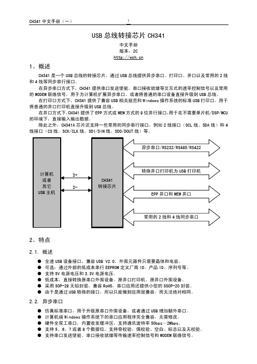
USB总线转接芯片CH341中文手册版本:2C1、概述CH341是一个USB总线的转接芯片,通过USB总线提供异步串口、打印口、并口以及常用的2线和4线等同步串行接口。
在异步串口方式下,CH341提供串口发送使能、串口接收就绪等交互式的速率控制信号以及常用的MODEM联络信号,用于为计算机扩展异步串口,或者将普通的串口设备直接升级到USB总线。
在打印口方式下,CH341提供了兼容USB相关规范和Windows操作系统的标准USB打印口,用于将普通的并口打印机直接升级到USB总线。
在并口方式下,CH341提供了EPP方式或MEM方式的8位并行接口,用于在不需要单片机/DSP/MCU 的环境下,直接输入输出数据。
除此之外,CH341A芯片还支持一些常用的同步串行接口,例如2线接口(SCL线、SDA线)和4线接口(CS线、SCK/CLK线、SDI/DIN线、SDO/DOUT线)等。
2、特点2.1. 概述●全速USB设备接口,兼容USB V2.0,外围元器件只需要晶体和电容。
●可选:通过外部的低成本串行EEPROM定义厂商ID、产品ID、序列号等。
●支持5V电源电压和3.3V电源电压。
●低成本,直接转换原串口外围设备、原并口打印机、原并口外围设备。
●采用SOP-28无铅封装,兼容RoHS,串口应用还提供小型的SSOP-20封装。
●由于是通过USB转换的接口,所以只能做到应用层兼容,而无法绝对相同。
2.2. 异步串口●仿真标准串口,用于升级原串口外围设备,或者通过USB增加额外串口。
●计算机端Windows操作系统下的串口应用程序完全兼容,无需修改。
●硬件全双工串口,内置收发缓冲区,支持通讯波特率50bps~2Mbps。
●支持5、6、7或者8个数据位,支持奇校验、偶校验、空白、标志以及无校验。
●支持串口发送使能、串口接收就绪等传输速率控制信号和MODEM联络信号。
●通过外加电平转换器件,提供RS232、RS485、RS422等接口。
TS431中文资料

1/9s LOW VOLTAGE OPERATION : 1.24 TO 6V s 2%, 1% AND 0.5% VOLTAGE PRECISION s WIDE OPERATING RANGE CATHODE CURRENT : 60µA TO 30mAs LOW OUTPUT IMPEDANCE : 0.2Ωs TYPICALLY STABLE FOR ANY CAPACI-TIVE LOADSs ESD PROTECTION :2kV (Human Body Model)200V (Machine Model)s100ppm/°C TEMPERATURE COEFFICIENTDESCRIPTIONThe TS431 is a low voltage three terminals pro-grammable shunt Voltage Reference. The output voltage can be set to any value between Vref (1.24V) and 6V with two external resistors. The TS431 is able to operate at a lower voltage (1.24V) and lower cathode current than the wide-spread TL431 and TL1431 shunt voltage refer-ence.When driving an optocoupler, the TS431 is partic-ularly interesting to regulate 3.3V switching power supplies.ORDER CODEZ = TO92 Plastic package - also available in Bulk (Z), Tape & Reel (ZT)and Ammo Pack (AP)LT = Tiny Package (SOT23-5) - only available in Tape & Reel (LT)PIN CONNECTIONS (top view)Part Number Temperature RangePackage SOT-23Marking Z L TS431I -40°C, +125°C••L272TS431AI ••L271TS431BI••L270TO92(Top view)SOT23-5(Top view)TS431LOW VOLTAGE ADJUSTABLE SHUNT REFERENCEApril 2002TS4312/9ABSOLUTE MAXIMUM RATINGSOPERATING CONDITIONSELECTRICAL CHARACTERISTICS T amb = 25°C (unless otherwise specified)Symbol ParameterValue Unit V KA Cathode to Anode Voltage10V I k Continuous Cathode Current Range -20 to +40mA I ref Reference Input Current Range-0.05 to +3mA P d Power Dissipation 1) TO92 packageSOT23-5 package 625500mW T stdStorage Temperature Range-65 to +150°C1.T junction =150°C, T amb =25°C with R THj-a =200°C/W for TO92 package and R THj-a =250°C/W for SOT23-5L packageSymbol ParameterValue Unit V KA Cathode to Anode Voltage 1.24 to 6V I k Cathode Current0.06 to 30mA T operOperating Free Air Temperature Range-40 to +125°CSymbol ParameterTest Condition Min.Typ.Max.Unit VrefOutput VoltageV KA = V ref @ I k = 100µA TS431TS431A TS431B1.2151.2281.2341.2401.2651.2521.246V∆V refOutput Voltage Change 1) 2)I k = 100µA, V KA = V re f1.Limits are 100% production tested at 25°C. Limits over temperature are guaranteed through correlation and by design.2.∆V ref is defined as the difference between the maximum and minimum values obtained over the full temperature range.∆V ref = V ref max. - V ref min.0 < T amb < +70°C -40 < T amb < +85°C -40 < T amb < +105°C -40 < T amb < +125°C 9161821mVRatio of Change in Reference InputVoltage to Change in Cathode to Anode VoltageI K = 10mAV KA = 6V to V ref 1.8 2.7mV/V I ref Reference Input CurrentI K = 10mA70160nA ∆I ref Reference Input Current Deviation Over Temperature RangeI K =10mA R 1=10k Ω R 2=∝-40 < T amb < +85°C -40 < T amb < +125°C 7090160240nA I min Minimum Cathode Current for Regulation V KA = V ref 4060µA I off Off-State Cathode Current V KA = 6V , V ref = 00.0010.1µA R KAStatic ImpedanceV KA = V ref ,I K = 0.1 to 15mA0.20.4Ω∆Vref ∆Vka ----------------TS4313/9Reference voltage vs temperatureCathode voltage vs cathode currentReference input current vs temperatureTest circuit for Vka = VrefCathode voltage vs cathode currentStatic impedance vs temperatureTS4314/9Off-State current vs temperatureRatio of change in reference input voltage to change in Vka voltage vs temperaturePhase and Gain vs frequencyTest c ircuit f or O ff-State c urrent m easurementTest circuit for Vka > VrefTest circuit for phase and gain measurementTS4315/9Pulse response at Ik=100µAPulse response at Ik = 1mAEquivalent input noise vs frequencyTest circuit for pulse response at Ik = 100µATest circuit for pulse response at Ik = 1mATS4316/9PACKAGE MECHANICAL DATA3 PINS - PLASTIC PACKAGE TO92 (TAPE & REEL)limetersInches MinTyp.Max.Min.Typ.Max.AL 5.00.197A 5.00.197T 4.00.157d 0.450.018I1 2.50.098P 11.712.713.70.4610.5000.539PO 12.412.7130.4880.5000.512P2 5.95 6.35 6.750.2340.2500.266F1/F2 2.4 2.5 2.80.0940.0980.110∆h -101-0.03900.039∆P -101-0.03900.039W 17.518.019.00.6890.7090.748W0 5.76 6.30.2240.2360.248W18.599.750.3350.3540.384W20.50.020H 200.787H015.51616.50.6100.6300.650H1250.984DO 3.84.04.20.1500.1570.165L1110.433TS4317/9PACKAGE MECHANICAL DATA3 PINS - PLASTIC PACKAGE TO92 (TAPE AMMO PACK)limetersInches MinTyp.Max.Min.Typ.Max.AL 5.00.197A 5.00.197T 4.00.157d 0.450.018I1 2.50.098P 11.712.713.70.4610.5000.539PO 12.412.7130.4880.5000.512P2 5.95 6.35 6.750.2340.2500.266F1/F2 2.4 2.5 2.80.0940.0980.110∆h -101-0.03900.039∆P -101-0.03900.039W 17.518.019.00.6890.7090.748W0 5.76 6.30.2240.2360.248W18.599.750.3350.3540.384W20.50.020H 200.787H015.51616.50.6100.6300.650H1250.984DO 3.84.04.20.1500.1570.165L1110.433TS4318/9PACKAGE MECHANICAL DATA3 PINS - PLASTIC PACKAGE TO92 (BULK)limetersInches Min Typ.Max.Min.Typ.Max.L 1.270.05B 3.2 3.7 4.20.1260.14570.1654O1 4.45 5.00 5.20.17520.19690.2047C 4.58 5.03 5.330.18030.1980.2098K 12.70.5O20.4070.50.5080.0160.01970.02a0.350.0138TS4319/9PACKAGE MECHANICAL DATA5 PINS - TINY PACKAGE (SOT23-5)DimensionsMillimetersInches Min.Typ.Max.Min.Typ.Max.A 0.90 1.20 1.450.0350.0470.057A100.150.006A20.90 1.05 1.300.0350.0410.051B 0.350.400.500.0140.0160.020C 0.090.150.200.0040.0060.008D 2.802.903.000.1100.1140.118D1 1.900.075e 0.950.037E 2.60 2.80 3.000.1020.1100.118F 1.50 1.60 1.750.0590.0630.069L 0.30.50.600.0120.0140.024K0d 10d 0d10dInformation furnished is believed to be accurate and reliable. However, STMicroelectronics assumes no responsibility for the consequences of use of such information nor for any infringement of patents or other rights of third parties which may result from its use. No license is granted by implication or otherwise under any patent or patent rights of STMicroelectronics. Specifications mentioned in this publication are subject to change without notice. This publication supersedes and replaces all information previously supplied. STMicroelectronics products are not authorized for use as critical components in life support devices or systems without express written approval of STMicroelectronics.© The ST logo is a registered trademark of STMicroelectronics© 2002 STMicroelectronics - Printed in Italy - All Rights ReservedSTMicroelectronics GROUP OF COMPANIESAustralia - Brazil - Canada - China - Finland - France - Germany - Hong Kong - India - Israel - Italy - Japan - MalaysiaMalta - Morocco - Singapore - Spain - Sweden - Switzerland - United Kingdom - United States© 。
APL431LBDC-TR中文资料
APL431LANPEC reserves the right to make changes to improve reliability or manufacturability without notice, and advise customers to obtain the latest version of relevant information to verify before placing orders.FeaturesGeneral DescriptionApplicationsThe APL431L is a 3-terminal low voltage adjustable precision reference with specified thermal stability over applicable commercial temperature ranges. Out-put voltage may be set to any value between V ref (1.24 V) and 20 V with two external resistors (see Fig-ure 2). When used with an photocoupler, the APL431L is an ideal voltage reference in isolated feed-back circuits for 3V to 12V switching-mode power supplies. This device has a typical output imped-ance of 0.1Ω. Active output circuitry provides a very sharp turn-on characteristic, making the APL431L ex-cellent replacements for zener diodes in many applications, including on-board regulation and ad-justable power supplies.• Precise Reference Voltage to 1.24V• Guaranteed 0.5% or 1% Reference VoltageTolerance• Sink Current Capability, 80uA to 100mA • Quick Turn-on• Adjustable Output Voltage, V O = V REF to 20V • Low Operational Cathode Current, 80µATypical• 0.1Ω Typical Output Impedance• SOT-23-3, SOT-23-5, TO-92 and SOT-89Packages• Lead Free Available (RoHS Compliant)• Linear Regulators• Adjustable Power Supply • Switching Power SupplySymbolFunctional DiagramSOT-23-3 (Top View)REF ANODECATHODE123SOT-89 (Top View)REFANODE CATHODE123REFANODECATHO DE321TO-92 (Top View)CathodeAnodeREFREF NCCATHODENCANODE 12345SOT-23-5 (Top View)APL431LOrdering and Marking InformationNotes: ANPEC lead-free products contain molding compounds/die attach materials and 100% matte in plate termination finish; which are fully compliant with RoHS and compatible with both SnPb and lead-free soldiering operations. ANPEC lead-free products meet or exceed the lead-free requirements of IPC/JEDEC J STD-020C for MSL classification at lead-free peak reflow temperature.Absolute Maximum RatingsAPL431LElectrical Characteristics T A = 25°C ( unless otherwise noted)Notes : 1.Full temperature range is 0°C to 70°C for APL431LXXC,and -40°C to 85°C for APL431LXXl.Test FiguresFigure 1. Test Circuit for V KA =V REF , V O =V KA =V REF Figure 3. Test Circuit for I K(off)V INV oAPL431LTest Figures (Cont.)Figure 2. Test Circuit for V KA >V REF ,V O = V KA = V REF × (1+R 1/R 2) + I REF × R 1V INV oApplication SchematicV oVPrecision Voltage ReferenceV oV INPrecision High-Current Series RegulatorNotes for Application Circuits:1) T o improve the stability of output voltage, a 0.1µF capacitor between cathode and anode of APL431L is strongly recommended.2)Set V OUT according to the following equation: V OUT = V REF (1+R1/R2)+l REF R13)Choose the value for R B as follows:A)The maximum limit for R B should be such that the cathode current(l K ) is greater than the mini mum operating current (80µA) at V IN(MIN). B)The minimum limit for RB should be such that the cathode current (l K ) does not exceed 100mA under all load conditions, and the instantaneous turnon value for lk does not exceed 150mA. Both of the following conditions must. be met: V IN(MAX)150mA V IN(MAX)-V OUTl OUT(MIN)+100mA(to limit instantaneous turn-on l K ) R B,Min ≥(to limit l K under normal operating conditions)R B,Min ≥0.080.100.120.140.160.18-50-252550751001251501.221.231.241.251.26-50-25255075100125150Junction Temperature (°C)R e f e r e n c e V o l t a g e (V )R e f e r e n c e I n p u t C u r r e n t (µA )Junction Temperature (°C)Referemce Voltage vs.Junction TemperatureReference Input Current vs.Junction TemperatureAPL431L0.10.20.30.40.5-50-252550751001251500Sµ01V5Sµ3V0Sµ5Sµ01V03VTypical CharacteristicsInputR a t i o o f D e l t a R e f e r e n c e V o l t a g e t oJunction Temperature (°C)O f f S t a t e C a t h o d e C u r r e n t (µA )Off State Cathode Current vs.Junction Temperature/∆V vs. Junction TemperatureI KA =1mAOutputInputOutputT A =25°CI KA =0.1mAT A =25°CAPL431L1020304050607080901000.00010.0010.010.11-100102030405060501001502002503003500.010.1110100101001000100001000001000000Typical CharacteristicsFrequency (Hz)Z k a (Ω)Frequency (Hz)G a i n (d B )P h a s e S h i f t (d e g r e e )Gain vs. Phase Shift vs. FrequencyZka vs. FrequencyLoad Capacitance (µF)I k (m A )Stability Boundary ConditionsAPL431LPackage Information SOT-23APL431LPackage Information SOT-23-5APL431LPackage Information TO-92APL431LPackage InformationSOT-89 (Reference EIAJ ED-7500A Reg stration SC-62)APL431LPhysical SpecificationsT LT P25T e m p e r a t u r eTim eReflow Condition (IR/Convection or VPR Reflow)Classificatin Reflow ProfilesAPL431LReliability Test ProgramCarrier Tape & Reel DimensionsAPL431LCarrier Tape & Reel DimensionsCarrier Tape & Reel Dimensions(mm)APL431LCover Tape DimensionsCustomer ServiceAnpec Electronics Corp.Head Office :5F, No. 2 Li-Hsin Road, SBIP,Hsin-Chu, T aiwan, R.O.C.T el : 886-3-5642000Fax : 886-3-5642050Taipei Branch :7F, No. 137, Lane 235, Pac Chiao Rd.,Hsin Tien City, Taipei Hsien, Taiwan, R. O. C.T el : 886-2-89191368Fax : 886-2-89191369。
- 1、下载文档前请自行甄别文档内容的完整性,平台不提供额外的编辑、内容补充、找答案等附加服务。
- 2、"仅部分预览"的文档,不可在线预览部分如存在完整性等问题,可反馈申请退款(可完整预览的文档不适用该条件!)。
- 3、如文档侵犯您的权益,请联系客服反馈,我们会尽快为您处理(人工客服工作时间:9:00-18:30)。
IKA(min)
-200
-2
-1
0
1
2
3
Cathode Voltage (V)
Fig 4 Pulse Response
7
Ta=25k
6
5
4
3
2
1
0
0
12
3
4
5
6
7
Time (µs)
Fig 6 Small Signal Voltage Amplification Vs Frequency
2
元器件交易网
UTC431
LINEAR INTEGRATED CIRCUIT
TEST CIRCUITS
INPUT
VKA IKA
VREF
UTC431
INPUT
R1 IREF
R2 VREF
VKA IKA
UTC431
INPUT
VKA IKA(OFF)
UTC431
VKA=VREF*(1+R1/R2)+IREF*R1
VKA
VREF
Cathode Current
IKA
1.0
Max 36 100
Unit V mA
ELECTRICAL CHARACTERISTICS(Ta=25°C,unless otherwise specified)
Characteristic
Symbol
Test conditions
MIN TYP MAX UNIT
Fig 7 Test Circuit For VKA=VREF
Fig 8 Test Circuit for VKAVREF
Fig 9 Test Circuit For IKA(OFF)
TYPICAL APPLICATION
Vi
Vo
Vi
Vo
Vi
IN UTC7805 OUT
Vo
COMMON
R1
R1
R1
IKA(OFF)
Dynamic Impedance
ZKA
Note TMIN=0°C,TMAX=+70°C
VKA=VREF,IKA=10mA TMIN≤TA≤TMAX IKA=10mA ∆VKA=10V~VREF
∆VKA=36V~10V IKA=10mA,R1=10k¡,R2=∞ IKA=10mA,R1=10kΩ,R2=∞ TA= full Temperature VKA=VREF
1
TO-92 1:Ref; 2:Anode; 3:Cathode
REFERENCE 2.5V Vref
CATHODE
REFERENCE (R)
CATHODE (K)
ANODE(A)
ANODE
YOUW ANG ELECTRONICS CO.LTD
1
元器件交易网
UTC431
125
100
Ta=25k VKA=VREF
75
50
25
0
-25
-50
-75
-100
-2
-1
0
1
2
3
Cathode Voltage (V)
Fig 3 Change in Reference Input Voltage Vs Cathode voltage
0
-5
IKA=100mA
-10
Ta=25k
-15
3
元器件交易网
UTC431
LINEAR INTEGRATED CIRCUIT
TYPICAL PERFORMANCE CHARACTERISTICS
Cathode Current (mA)
Change In Reference INput Voltage (mV)
Fig 1 Cathode Current Vs Cathode Voltage
元器件交易网
UTC431
LINEAR INTEGRATED CIRCUIT
PROGRAMMABLE PRECISION REFERENCE
DESCRIPTION
The UTC431 is three-terminal adjustable regulator with a guaranteed thermal stability over applicable temperature ranges. The output Voltage may be set to any value between Vref(approximately 2.5V) and 26 V with two external resistors.These devices have provides a very sharp turn-on characteristic, making these devices excellent replacement for zener diodes in many applications.
Reference Input Current
Iref
Deviation of Reference Input Current ∆Iref/∆T
Over Ful l Temperature Range
Minimum cathode current for
IKA(min)
regulation
Off-state cathode Current
103
104
105
106
107
Frequency (Hz)
Cathode Current (µA)
Voltage Amplification (dB)
Input and Output Voltage (V)
800 600 400 200 0
Fig 2 Cathode Current Vs Cahode Voltage
LINEAR INTEGRATED CIRCUIT
ABSOLUTE MAXIMUM RATINGS (Operating temperature range applies unless otherwise specified))
CHARACTERISTICS
SYMBOL
VALUE
UNITS
Cathode Voltage
Vi
Io Vo
Vi
Io
Vo
RCL
Rs
UTCnt-current Sink
UTC431 RS=VREF/RCL
Fig 14 Current Limiting or Current Source
YOUW ANG ELECTRONICS CO.LTD
1000
mW
Operating temperature
Topr
0~70
°C
Storage temperature Temperature
Tstg
-65~+150 °C
°C
RECOMMENDED OPERATING CONDITIONS
Characteristic
Symbol
Min
Typ
Cathode Voltage
FEATURE
*Programmable output Voltage to 36V *Low dynamic output impedance 0.2Ω *Sink current capability of 1.0 to 100mA *Equivalent full-range temperature coefficient of 50ppm/°C
Reference Input Voltage
Vref
VKA=VREF,IKA=10mA
2.440 2.495 2.550 V
Deviation of reference Input Voltage ∆Vref/∆T Over temperature(note 1) Ratio of Change in Reference Input ∆Vref/∆VKA Voltage to the Change in Cathode Voltage
-20
-25
-30
-35
-40 0
5
10 15 20 25 30 35 40
Cathode Voltage (V)
Fig 5 Dynamic Impedance Vs Frequency
102 Ta=25k
Ta=25k IKA=1mA~100mA IKA=0mA to 100mA
101
10 0
10-1
70
60
Ta=25k
IKA=10mA
50
40
30
20 10 0
-10
103
104
105
106
107
Frequency (Hz)
Impedance (Ω)
YOUW ANG ELECTRONICS CO.LTD
4
typical *Temperature compensated for operation over full rated
operating temperature range *Low output noise voltage *Fast turn on response
BLOCK DIAGRAM
VKA
37
V
Cathode Current Range(Continuous)
IKA
-100~+150
mA
Reference Input Current Range
Iref
0.05~+10
mA
Power Dissipation
