A3P250
Actel FPGA介绍

Actel ProASIC3/E系列特性
先进的I/O
用户最多可用616个单端I/O或300个差分I/O,支持多种I/O电平 标准和Bank电压。
单端I/O最快速度可达 250MHZ,差分可达 350MHZ,DDR可达到 700MHZ
Actel ProASIC3/E系列特性
先进的I/O
用户最多可用616个单端I/O或300个差分I/O,支持多种I/O电平 标准和Bank电压。
四种布线资源
以最小的延时跨越整个器件,垂直方向可以跨越正负12个VersaTile,
超快速的局部连线资源
四 种 布 线 资 源
有效长线资源
高速的超长线资源
高新能全局网络
Actel FPGA的布线结构
为片上全局网络和象限全局网络。
四种布线资源
应用于需要低偏斜、低延时、低抖动、高扇出的网点。全局网络分
ProASIC3L
具有独特的
Flash*Freeze 技术,功耗低
Fusion
具有分辨率为
12位,转换速率 为600KSPS的 ADC
IGLOO
静态功耗低至
5UW,并保存 RAM数据
IGLOO+
应用于低功耗,
高性能I/O的场 合
Nano
成本低至1$
商业级温度范
围更广(-200c~ 700c)
应用于低功耗,
JTAG Port
Actel Fusion系列
GPIO
嵌入式Flash内存
Flash memory区块(2M)
MOSFET Outputs Analog Inputs
A/D
A3P FPGA Fabric (incl. SRAM, CCC/PLL, IO)
FKP250A资料

(1) Gate(2) Drain (1) (2)(3)(3) SourceCAUTION / WARNING●The information in this publication has been carefully checked and is believed to be accurate; however, no responsibility is assumed for inaccuracies.● Sanken reserves the right to make changes without further notice to any products herein in the interest of improvements in the performance, reliability, or manufacturability of its products.Before placing an order, Sanken advises its customers to obtain the latest version of the relevant information to verify that the information being relied upon is current.● Application and operation examples described in this catalog are quoted for the sole purpose of reference for the use of the products herein and Sanken can assume no responsibility for any infringement of industrial property rights, intellectual property rights or any other rights of Sanken or any third party which may result from its use.● When using the products herein, the applicability and suitability of such products for the intended purpose or object shall be reviewed at the users’ responsibility.● Although Sanken undertakes to enhance the quality and reliability of its products, the occurrence of failure and defect of semiconductor products at a certain rate is inevitable. Users of Sanken products are requested to take, at their own risk, preventative measures including safety design of the equipment or systems against any possible injury, death, fires or damages to the society due to device failure or malfunction.● Sanken products listed in this catalog are designed and intended for the use as components in general purpose electronic equipment or apparatus (home appliances, office equipment, telecommunication equipment, measuring equipment, etc.). Before placing an order, the user’s written consent to the specifications is requested.When considering the use of Sanken products in the applications where higher reliability is required (transportation equipment and its control systems, traffic signal control systems or equipment, fire/crime alarm systems, various safety devices, etc.), please contact your nearest Sanken sales representative to discuss and obtain written confirmation of your specifications. The use of Sanken products without the written consent of Sanken in the applications where extremely high reliability is required (aerospace equipment, nuclear power control systems, life support systems, etc.) is strictly prohibited.● Anti radioactive ray design is not considered for the products listed herein.● This publication shall not be reproduced in whole or in part without prior written approval from Sanken.●This is notification that you, as purchaser of the products/technology, are not allowed to perform any of the following:1. Resell or retransfer these products/technology to any party intending to disturb international peace and security.2. Use these products/technology yourself for activities disturbing international peace and security.3. Allow any other party to use these products/technology for activities disturbing international peace and security. Also, as purchaser of these products/technology, you agree to follow the procedures for the export or transfer of these products/technology, under the Foreign Exchange and Foreign Trade Law, when you export or transfer theproducts/technology abroad.。
施耐德断路器nse250h 3p 250a
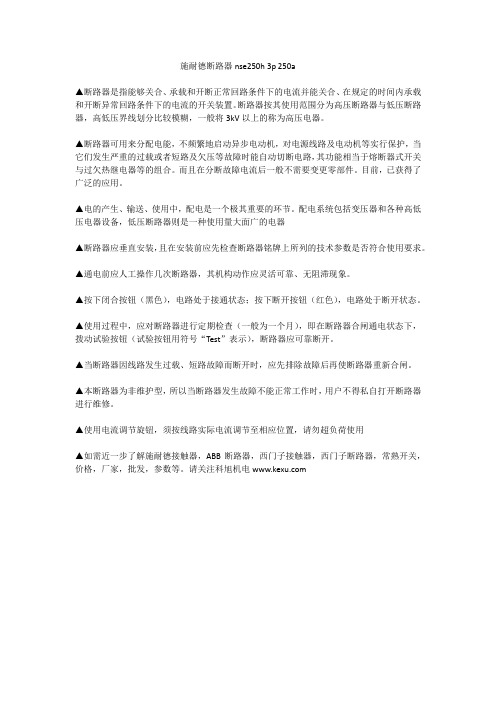
施耐德断路器nse250h 3p 250a
▲断路器是指能够关合、承载和开断正常回路条件下的电流并能关合、在规定的时间内承载和开断异常回路条件下的电流的开关装置。
断路器按其使用范围分为高压断路器与低压断路器,高低压界线划分比较模糊,一般将3kV以上的称为高压电器。
▲断路器可用来分配电能,不频繁地启动异步电动机,对电源线路及电动机等实行保护,当它们发生严重的过载或者短路及欠压等故障时能自动切断电路,其功能相当于熔断器式开关与过欠热继电器等的组合。
而且在分断故障电流后一般不需要变更零部件。
目前,已获得了广泛的应用。
▲电的产生、输送、使用中,配电是一个极其重要的环节。
配电系统包括变压器和各种高低压电器设备,低压断路器则是一种使用量大面广的电器
▲断路器应垂直安装,且在安装前应先检查断路器铭牌上所列的技术参数是否符合使用要求。
▲通电前应人工操作几次断路器,其机构动作应灵活可靠、无阻滞现象。
▲按下闭合按钮(黑色),电路处于接通状态;按下断开按钮(红色),电路处于断开状态。
▲使用过程中,应对断路器进行定期检查(一般为一个月),即在断路器合闸通电状态下,拨动试验按钮(试验按钮用符号“Test”表示),断路器应可靠断开。
▲当断路器因线路发生过载、短路故障而断开时,应先排除故障后再使断路器重新合闸。
▲本断路器为非维护型,所以当断路器发生故障不能正常工作时,用户不得私自打开断路器进行维修。
▲使用电流调节旋钮,须按线路实际电流调节至相应位置,请勿超负荷使用
▲如需近一步了解施耐德接触器,ABB断路器,西门子接触器,西门子断路器,常熟开关,价格,厂家,批发,参数等。
请关注科旭机电。
HDSP-2503资料

Eight Character 5 mm and 7 mm Smart Alphanumeric Displays Technical DataFeatures• X Stackable (HDSP-21XX)• XY Stackable (HDSP-250X)• 128 Character ASCII Decoder• Programmable Functions • 16 User Definable Characters• Multi-Level Dimming and Blanking• TTL Compatible CMOS IC • Wave SolderableApplications• Computer Peripherals• Industrial Instrumentation • Medical Equipment• Portable Data Entry Devices • Cellular Phones • TelecommunicationsEquipment• Test EquipmentDescriptionThe HDSP-210X/-211X/-250Xseries of products is ideal forapplications where displayingeight or more characters of dotmatrix information in anaesthetically pleasing manner isrequired. These devices are8-digit, 5 x 7 dot matrix, alpha-numeric displays and are allpackaged in a standard 15.24 mm(0.6 inch) 28 pin DIP. The on-board CMOS IC has the ability todecode 128 ASCII characterswhich are permanently stored inROM. In addition, 16 program-mable symbols may be stored inon-board ROM, allowing consider-HDSP-210X SeriesHDSP-211X SeriesHDSP-250X Seriesable flexibility for displayingadditional symbols and icons.Seven brightness levels provideversatility in adjusting the displayintensity and power consumption.The HDSP-210X/-211X/-250Xproducts are designed forstandard microprocessor interfacetechniques. The display andspecial features are accessedthrough a bidirectional 8-bit databus.Device Selection GuideAlGaAs High EfficiencyFont Height Red Red Orange Yellow Green0.2 inches HDSP-2107HDSP-2112HDSP-2110HDSP-2111HDSP-21130.27 inches HDSP-2504HDSP-2502HDSP-2500HDSP-2501HDSP-2503Package DimensionsESD WARNING: STANDARD CMOS HANDLING PRECAUTIONS SHOULD BE OBSERVED TO AVOID STATIC DISCHARGE.Absolute Maximum RatingsSupply Voltage, V DD to Ground [1]........................................-0.3 to 7.0 V Operating Voltage, V DD to Ground [2]..............................................5.5 V Input Voltage, Any Pin to Ground..............................-0.3 to V DD +0.3 V Free Air Operating Temperature Range, T A [3]................-45°C to +85°C Storage Temperature Range, T S ..................................-55°C to +100°C Relative Humidity (non-condensing)...............................................85%Maximum Solder Temperature(Below Seating Plane), t < 5 sec..............................................260°C ESD Protection @ 1.5 k Ω, 100 pF ........................V Z = 4 kV (each pin)Notes:1. Maximum Voltage is with no LEDs illuminated.2. 20 dots ON in all locations at full brightness.3. Maximum supply voltage is 5.25 V for operation above 70°C.Package DimensionsASCII Character Set HDSP-210X, HDSP-211X, HDSP-250X SeriesElectrical Characteristics Over Operating Temperature Range (-45°C to +85°C)4.5 V < V DD <5.5 V , unless otherwise specifiedT A = 25°C -45°C < T A < + 85°CV DD = 5.0 V 4.5 V < V DD < 5.5 V Parameter Symbol Typ.Max.Min.Max.Units Test Conditions Input LeakageI IH 1.0µAV IN = 0 to V DD ,(Input without pullup)I IL -1.0pins CLK, D 0-D 7,A 0-A 4Input CurrentI IPL-11-18-30µAV IN = 0 to V DD ,(Input with pullup)pins CLS, RST,WR, RD, CE, FL I DD BlankI DD (BLK)0.5 3.0 4.0mA V IN = V DD I DD 8 digitsI DD (V)200255330mA “V” on in all 812 dots/character [1,2]locations I DD 8 digitsI DD (#)300370430mA “#” on in all 20 dots/character [1,2,3,4]locationsInput Voltage High V IH 2.0V DD V +0.3Input Voltage Low V IL GND 0.8V -0.3 V Output Voltage High V OH 2.4VV DD = 4.5 V ,I OH = -40 µA Output Voltage Low V OL 0.4V V DD = 4.5 V ,D 0-D 7I OL = 1.6 mA Output Voltage Low V OL 0.4V V DD = 4.5 V ,CLKI OL = 40 µA High Level Output I OH -60mA V DD = 5.0 V CurrentLow Level Output I OL 50mA V DD = 5.0 VCurrentThermal Resistance R θJ-C15°C/WIC Junction-to-CaseNotes:1.Average I DD measured at full brightness. See Table 2 in Control Word Section for I DD at lower brightness levels. Peak I DD = 28/15 x I DD (#).2.Maximum I DD occurs at -55°C.3.Maximum I DD (#) = 355 mA at V DD = 5.25 V and IC T J = 150°C.4.Maximum I DD (#) = 375 mA at V DD =5.5 V and IC T J = 150°C.Optical Characteristics at 25°CV DD = 5.0 V at Full BrightnessLuminous Intensity Peak DominantCharacter Average (#)Wavelength Wavelength Part Iv (mcd)λPeakλd Description Number Min.Typ.(nm)(nm) AlGaAs HDSP-2107 5.015.0645637-2504HER HDSP-2112 2.57.5635626-2502Orange HDSP-2110 2.57.5600602-2500Yellow HDSP-2111 2.57.5583585-2501High HDSP-2113 2.57.5568574 Performance -2503GreenNote: 1. Refers to the initial case temperature of the device immediately prior to measurement.[1]AC Timing Characteristics Over Temperature Range (-45°C to +85°C)4.5 V < V DD <5.5 V, unless otherwise specifiedReferenceNumber Symbol Description Min.[1]Units 1t ACC Display Access TimeWrite210Read230ns 2t ACS Address Setup Time to Chip Enable10ns 3t CE Chip Enable Active Time[2,3]Write140Read160ns 4t ACH Address Hold Time to Chip Enable20ns 5t CER Chip Enable Recovery Time60ns 6t CES Chip Enable Active Prior to Rising Edge of[2,3]Write140Read160ns 7t CEH Chip Enable Hold Time to Rising Edge ofRead/Write Signal[2,3]0ns 8t W Write Active Time100ns 9t WSU Data Write Setup Time50ns 10t WH Data Write Hold Time20ns 11t R Chip Enable Active Prior to Valid Data160ns 12t RD Read Active Prior to Valid Data75ns 13t DF Read Data Float Delay10ns t RC Reset Active Time[4]300ns Notes:1. Worst case values occur at an IC junction temperature of 150° C.2. For designers who do not need to read from the display, the Read line can be tied to VDD and the Write and Chip Enable lines can betied together.3. Changing the logic levels of the Address lines when CE = “0” may cause erroneous data to be entered into the Character RAM,regardless of the logic levels of the WR and RD lines.4. The display must not be accessed until after 3 clock pulses (110 µs min. using the internal refresh clock) after the rising edge of thereset line.AC Timing Characteristics Over Temperature Range (-45°C to +85°C)4.5 V < V DD <5.5 V , unless otherwise specifiedWrite Cycle Timing DiagramSymbol Description 25°C Typ.Min.[1]Units F OSC Oscillator Frequency 5728kHz F RF [2]Display Refresh Rate 256128Hz F FL [3]Character Flash Rate 21Hz t ST [4]Self Test Cycle Time4.69.2secNotes:1. Worst case values occur at an IC junction temperature of 150°C.2. F RF = F OSC/2243. F FL = F OSC /28,6724. t ST = 262,144/F OSCRead Cycle Timing DiagramRelative Luminous Intensity vs. TemperatureYELLOW HDSP-2111/2501Electrical DescriptionPin Function DescriptionRESET (RST, pin 1)Initializes the display.FLASH (FL, pin 2)FL low indicates an access to the Flash RAM and is unaffected by thestate of address lines A3-A4.ADDRESS INPUTS Each location in memory has a distinct address. Address inputs (A0-A2)(A0-A4, pins 3-6, 10)select a specific location in the Character RAM, the Flash RAM or aparticular row in the UDC (User-Defined Character) RAM. A3-A4 areused to select which section of memory is accessed. Table 1 shows thelogic levels needed to access each section of memory.Table 1. Logic Levels to Access MemorySection of Memory FL A4 A3A2 A1 A0Flash RAM 0X X Char. AddressUDC Address Register 10 0Don't CareUDC RAM 10 1Row AddressControl Word Register 11 0Don’t CareCharacter RAM 11 1Character Address CLOCK SELECT Used to select either an internal (CLS = 1) or external (CLS = 0) clock source. (CLS, pin 11)CLOCK INPUT/OUTPUT Outputs the master clock (CLS = 1) or inputs a clock (CLS = 0) for slave (CLK, pin 12)displays.WRITE (WR, pin 13)Data is written into the display when the WR input is low and theCE input is low.CHIP ENABLE (CE, pin 17)Must be at a logic low to read or write data to the display and must gohigh between each read and write cycle.READ (RD, pin 18)Data is read from the display when the RD input is low and the CEinput is low.DATA Bus (D0-D7,Used to read from or write to the display.pins 19, 20, 23-28)GND (SUPPLY) (pin 15)Analog ground for the LED drivers.GND (LOGIC) (pin 16)Digital ground for internal logic.V DD (POWER) (pin 14)Positive power supply input.F i g u r e 1. H D S P -210X /-211X /-212X /-250X I n t e r n a l B l o c k D i a g r a m .11Character RAM This RAM stores either ASCII character data or a UDC RAM address.Flash RAMThis is a 1 x 8 RAM which stores Flash data.User-Defined Character RAM This RAM stores the dot pattern for custom characters.(UDC RAM)User-Defined Character This register is used to provide the address to the UDC RAM when Address Registerthe user is writing or reading a custom character.(UDC Address Register)Control Word RegisterThis register allows the user to adjust the display brightness, flash individual characters, blink, self test, or clear the display.Display Internal Block DiagramFigure 1 shows the internal block diagram of the HDSP-210X/-211X/-250X displays. The CMOS IC consists of an 8 byte CharacterRAM, an 8 bit Flash RAM, a 128character ASCII decoder, a 16character UDC RAM, a UDCAddress Register, a Control Word Register, and refresh circuitry necessary to synchronize thedecoding and driving of eight 5 x 7 dot matrix characters. Themajor user-accessible portions of the display are listed below:Character RamFigure 2 shows the logic levels needed to access theHDSP-210X/-211X/-250XCharacter RAM. During a normal access, the CE = “0” and either RD = “0” or WR = “0.” However,erroneous data may be written into the Character RAM if the address lines are unstable when CE = “0” regardless of the logic levels of the RD or WR lines.Address lines A 0-A 2 are used to select the location in the Charac-ter RAM. Two types of data can be stored in each Character RAM location: an ASCII code or a UDC RAM address. Data bit D 7 is used to differentiate between the ASCII character and a UDC RAMaddress. D 7 = 0 enables the ASCII decoder and D 7 = 1 enables the UDC RAM. D 0-D 6 are used to input ASCII data and D 0-D 3 are used to input a UDC address.Figure 2. Logic Levels to Access the Character RAM.12 UDC RAM and UDC AddressRegisterFigure 3 shows the logic levelsneeded to access the UDC RAMand the UDC Address Register.The UDC Address Register iseight bits wide. The lower fourbits (D0-D3) are used to select oneof the 16 UDC locations. Theupper four bits (D4-D7) are notused. Once the UDC address hasbeen stored in the UDC AddressRegister, the UDC RAM can beaccessed.To completely specify a 5 x 7character, eight write cycles arerequired. One cycle is used tostore the UDC RAM address in theUDC Address Register and sevencycles are used to store dot datain the UDC RAM. Data is enteredby rows and one cycle is neededto access each row. Figure 4shows the organization of a UDCcharacter assuming the symbol tobe stored is an “F.” A0-A2 are usedto select the row to be accessedand D0-D4 are used to transmitthe row dot data. The upper threebits (D5-D7) are ignored. D0 (leastsignificant bit) corresponds to theright most column of the 5 x 7matrix and D4 (most significantbit) corresponds to the left mostcolumn of the 5 x 7 matrix.Flash RAMFigure 5 shows the logic levelsneeded to access the Flash RAM.The Flash RAM has one bitassociated with each location ofthe Character RAM. The Flashinput is used to select the FlashRAM while address lines A3-A4 areignored. Address lines A0-A2 areused to select the location in theFlash RAM to store the attribute. D0 is used to store or remove the flash attribute. D0 = “1” stores the attribute and D0 = “0”removes the attribute.When the attribute is enabledthrough bit 3 of the Control Wordand a “1” is stored in the FlashRAM, the correspondingcharacter will flash at approxi-mately 2 Hz. The actual rate isdependent on the clock frequency.For an external clock the flashrate can be calculated by dividingthe clock frequency by 28,672.C C C C CO O O O OL L L L L12345UDC HEXD4D3D2D1D0CHARACTER CODE11111ROW 1*****1F10000ROW 2*1010000ROW 3*1011110ROW 4****1D10000ROW 5*1010000ROW 6*1010000ROW 7*10IGNORED0 = LOGIC 0; 1 = LOGIC 1; * = ILLUMINATED LED.Figure 4. Data to Load ""F'' into the UDC RAM.元器件交易网Figure 5. Logic Levels to Access the Flash RAM.Table 2. Current Requirements atDifferent Brightness Levels V DD = 5.0 V %Current at 25°CSymbol D 2D 1D 0BrightnessTyp.Units I DD (V)000100200mA 00180160mA 01053106mA 0114080mA 1002754mA 1012040mA 111326mAFigure 6. Logic Levels to Access the Control Word RegisterControl Word RegisterFigure 6 shows how to access the Control Word Register. This 8-bit register performs five functions:Brightness control, Flash RAM control, Blinking, Self Test, and Clear. Each function isindependent of the others; how-ever, all bits are updated during each Control Word write cycle.Brightness (Bits 0-2)Bits 0-2 of the Control Word adjust the brightness of the display. Bits 0-2 are interpreted as a three bit binary code with code (000) corresponding to maximum brightness and code (111) corresponding to a blanked display. In addition to varying the display brightness, bits 0-2 also vary the average value of I DD . I DD can be calculated at any bright-ness level by multiplying the percent brightness level by the value of I DD at the 100% bright-ness level. These values of I DD are shown in Table 2.Flash Function (Bit 3)Bit 3 determines whether the flashing character attribute is on or off. When bit 3 is a“1,” the output of the Flash RAM ischecked. If the content of a loca-tion in the Flash RAM is a “1,” the associated digit will flash atapproximately 2 Hz. For anexternal clock, the blink rate can be calculated by driving the clock frequency by 28,672. If the flash enable bit of the Control Word is a “0,” the content of the Flash RAM is ignored. To use this function with multiple display systems, see the Display Reset section.Blink Function (Bit 4)Bit 4 of the Control Word is used to synchronize blinking of alleight digits of the display. When this bit is a “1” all eight digits of the display will blink at approxi-mately 2 Hz. The actual rate is dependent on the clock frequency .For an external clock, the blink rate can be calculated by dividing the clock frequency by 28,672.This function will override the Flash function when it is active.To use this function with multiple display systems, see the Display Reset section.Self Test Function (Bits 5, 6) Bit 6 of the Control Word Register is used to initiate the self test function. Results of the internal self test are stored in bit 5 of the Control Word. Bit 5 is a read only bit where bit 5 = “1” indicates a passed self test and bit 5 = “0”indicates a failed self test.Setting bit 6 to a logic 1 will start the self test function. The built-in self test function of the IC consists of two internal routines which exercise major portions of the IC and illuminate all of the LEDs. The first routine cycles the ASCII decoder ROM through all states and performs a checksum on the output. If the checksum agrees with the correct value, bit 5 is set to “1.” The second routine provides a visual test of the LEDs using the drive circuitry. This is accomplished by writing checkered and inverse checkered patterns to the display. Each pattern is displayed for approxi-mately 2 seconds.During the self test function the display must not be accessed. The time needed to execute the self test function is calculated by multiplying the clock period by 262,144. For example, assume a clock frequency of 58 KHz, then the time to execute the self test function frequency is equal to (262,144/58,000) = 4.5 second duration.At the end of the self test func-tion, the Character RAM is loaded with blanks, the Control Word Register is set to zeros except for bit 5, the Flash RAM is cleared, and the UDC Address Register is set to all ones.Clear Function (Bit 7)Bit 7 of the Control Word willclear the Character RAM and theFlash RAM. Setting bit 7 to a “1”will start the clear function. Threeclock cycles (110 ms minimumusing the internal refresh clock)are required to complete the clearfunction. The display must not beaccessed while the display isbeing cleared. When the clearfunction has been completed, bit7 will be reset to a “0.” The ASCIIcharacter code for a space (20H)will be loaded into the CharacterRAM to blank the display and theFlash RAM will be loaded with“0”s. The UDC RAM, UDCAddress Register, and the re-mainder of the Control Word areunaffected.Display ResetFigure 7 shows the logic levelsneeded to Reset the display. Thedisplay should be Reset onPower-up. The external Resetclears the Character RAM, FlashRAM, Control Word and resetsthe internal counters. After therising edge of the Reset signal,three clock cycles (110 µsminimum using the internalrefresh clock) are required tocomplete the reset sequence. Thedisplay must not be accessedwhile the display is being reset.The ASCII Character code for aspace (20H) will be loaded intothe Character RAM to blank thedisplay. The Flash RAM andControl Word Register are loadedwith all “0”s. The UDC RAM andUDC Address Register areunaffected. All displays whichoperate with the same clocksource must be simultaneouslyreset to synchronize the Flashingand Blinking functions.Mechanical and ElectricalConsiderationsThe HDSP-210X/-211X/-250X are28 pin dual-in-line packages with26 external pins. The devices canbe stacked horizontally and verti-cally to create arrays of any size.The HDSP-210X/-211X/-250X aredesigned to operate continuouslyfrom -45°C to +85°C with amaximum of 20 dots on percharacter at 5.25 V. Illuminatingall thirty-five dots at full bright-ness is not recommended.The HDSP-210X/-211X/-250X areassembled by die attaching andwire bonding 280 LED chips anda CMOS IC to a thermallyconductive printed circuit board.A polycarbonate lens is placedover the PC board creating an airgap over the LED wire bonds. Aprotective cap creates an air gapover the CMOS IC. Backfill epoxyenvironmentally seals the displaypackage. This packageconstruction makes the displayhighly tolerant to temperaturecycling and allows wavesoldering.The inputs to the IC are protectedagainst static discharge and inputcurrent latchup. However, forbest results standard CMOShandling precautions should be Figure 7. Logic Levels to Reset theDisplay.15used. Prior to use, the HDSP-210X/-211X/-250X should be stored in antistatic tubes or in conductive material. During assembly, a grounded conductive work area should be used, and assembly personnel should wear conductive wrist straps. Lab coats made of synthetic material should be avoided since they are prone to static buildup. Input current latchup is caused when the CMOS inputs are subjected to either a voltage below ground (V IN < ground) or to a voltage higher than V DD (V IN > V DD) and when a high current is forced into the input. To prevent input current latchup and ESD damage, unused inputs should be con-nected either to ground or to V DD. Voltages should not be applied to the inputs until V DD has been applied to the display.Thermal Considerations The HDSP-210X/-211X/-212X/ 250X have been designed to provide a low thermal resistance path for the CMOS IC to the 26 package pins. Heat is typically conducted through the traces of the printed circuit board to free air. For most applications no additional heatsinking is required.Measurements were made on a 32 character display string to determine the thermal resistance of the display assembly. Several display boards were constructed using 0.062 in. thick printed circuit material, and one ounce copper 0.020 in. traces. Some of the device pins were connected to a heatsink formed by etching a copper area on the printed circuit board surrounding the display. A maximally metallized printed circuit board was also evaluated.The junction temperature wasmeasured for displays soldereddirectly to these PC boards,displays installed in sockets, andfinally displays installed insockets with a filter over thedisplay to restrict airflow. Theresults of these thermalresistance measurements, RθJ-Aare shown in Table 3 and includethe effects of RθJ-C.Ground ConnectionsTwo ground pins are provided tokeep the internal IC logic groundclean. The designer can, whennecessary, route the analogground for the LED driversseparately from the logic grounduntil an appropriate ground planeis available. On long interconnec-tions between the display and thehost system, the designer cankeep voltage drops on the analogground from affecting the displaylogic levels by isolating the twogrounds.The logic ground should beconnected to the same groundpotential as the logic interfacecircuitry. The analog ground andthe logic ground should beconnected at a common groundwhich can withstand the currentintroduced by the switching LEDdrivers. When separate groundconnections are used, the analogground can vary from -0.3 V to+0.3 V with respect to the logicground. Voltage below -0.3 V cancause all dots to be on. Voltageabove +0.3 V can cause dimmingand dot mismatch.Soldering and Post SolderCleaning Instructions forthe HDSP-210X/-211X/-250XThe HDSP-210X/-211X/-250Xmay be hand soldered or wavesoldered with SN63 solder. Whenhand soldering, it is recom-mended that an electronicallytemperature controlled andsecurely grounded soldering ironbe used. For best results, the irontip temperature should be set at315°C (600°F). For wave solder-ing, a rosin-based RMA flux canbe used. The solder wave temper-ature should be set at 245°C ±5°C (473°F ± 9°F), and the dwellin the wave should be setbetween 11 /2 to 3 seconds foroptimum soldering. The preheattemperature should not exceed105°C (221°F) as measured onthe solder side of the PC board. Table 3. Thermal Resistance, θJA, Using Various Amounts of Heatsinking MaterialHeatsinkingMetal W/Sockets W/O Sockets W/Sockets per Device W/O Filter W/O Filter W/Filter sq. in.(Avg.)(Avg.)(Avg.)Units 0313035°C/W1312833°C/W3302633°C/W Max. Metal292532°C/W 4 Board Avg302733°C/WFor additional information onsoldering and post solder clean-ing, see Application Note 1027,Soldering LED Components.Contrast EnhancementThe objective of contrastenhancement is to provide goodreadability in a variety of ambientlighting conditions. For informa-tion on contrast enhancement seeApplication Note 1015, ContrastEnhancement Techniques forLED Displays.Data subject to change.Copyright © 1999 Agilent Technologies, Inc.Obsoletes 5964-6378E5968-7907E (11/99)。
电子陀螺仪原理与构造

电子陀螺仪原理与构造名目:一、MEMS陀螺仪市场现状 (2)第一节、MEMS要紧厂家产品资料汇总 (2)第二节、MEMS在我国的产业现状 (2)二、MEMS陀螺仪介绍 (3)第一节、什么是微机械(MEMS)? (3)第二节、微机械陀螺仪(MEMS gyroscope)的工作原理 (3)第三节、微机械陀螺仪的结构 (4)三、MEMS技术的加工工艺 (6)第一节、体加工工艺 (6)第二节、硅表面微机械加工技术 (7)第三节、结合技术 (7)第四节、逐次加工 (8)第五节、LIGA工艺 (8)第六节、THEMLA工艺流程 (9)四、基于DSP的MEMS陀螺仪信号处理平台设计 (9)第一节、MEMS陀螺仪信号处理平台的硬件结构 (9)第二节、MEMS陀螺仪信号处理平台系统任务分析 (10)第三节、MEMS信号处理平台软件设计方案 (11)五、基于GPS的汽车导航系统的设计与实现 (12)第一节、主体操纵方案 (12)第二节、GPS定位系统设计 (13)第三节、车体部分MCU 主控模块设计 (14)第四节、系统软件设计 (14)一、MEMS陀螺仪市场现状MEMS陀螺仪即微机电系统陀螺仪,是一种微型传感器,要紧用于手机及游戏机等领域。
与一般芯片相比,除运算功能外,此产品还具有感知功能,通过内置的陀螺仪传感器能够感知外界运动,并做出相应反应。
在具体应用上,MEMS芯片能够用在消费类电子产品上,比如游戏机中的动作操纵;能够用在汽车安全领域,在汽车显现紧急情形时及时作出反应;在军事、航海中,陀螺仪被用来导航。
此前全球针对消费电子产品的陀螺仪厂商只有意法半导体(ST)、飞思卡尔半导体(Freescale)两家,深迪半导体( :// senodia )成为第三家,打破了国内众多消费电子厂商陀螺仪全部依靠进口的局面。
深迪半导体成立于2008年8月,目前在国内还没有竞争对手。
依照闻名市场研究顾问机构 Yole Development 的最新推测,MEMS 陀螺仪、加速度计和 IMU 的销售额在2020年将达到45亿美元的规模,在消费类应用市场的年增长率达到了27%,而中国以后将是消费类电子、汽车工业以及其产业链的中心和全球最大的市场。
FPGA接口设计研究
FPGA接口设计研究1EMIF16接口异步通信模式根据控制信号的特性,EMIF16在异步通信时有三种模式可选,分别是写触发模式(WEmode)、片选触发模式(CEmode)与外部等待模式(Extend-edWaitmode)。
其中,写触发模式默认通过驱动的3通道,其对应的地址空间为0x7C000000-0x7FFFFFFF,且不能伴随其他模式一同使用。
片选触发模式具备较强灵活性,能够适用于4个存取片区。
外部等待模式允许外部设备灵活插入异步硬件等待时间,本设计中采用了外部等待模式,具体读写时序如图2~3所示。
图2中,EM_*即对应1.1中提及的EMIF*信号,“14”代表等待信号EM_WAIT的建立时间,即EM_WAIT必须在/EM_OE跳高前(4E+3)ns内有效,才能正常插入外部等待;“11”代表外部等待的延迟时间,即EM_WAIT无效后/EM_OE的有效延迟时间,最大不超过(4E+3)ns;“2”代表EM_WAIT有效与无效时间最短时间为2E;其中E代表EMIF16的一个时钟周期。
图3中,EM_*同样对应1.1中提及的EMIF*信号,“28”代表等待信号EM_WAIT的建立时间,即EM_WAIT必须在/EM_WE跳高前(4E+3)ns内有效,才能正常插入外部等待;“25”代表外部等待的延迟时间,即EM_WAIT无效后/EM_WE的有效延迟时间,最大不超过(4E+3)ns;“2”代表EM_WAIT有效与无效时间最短时间为2E;其中E代表EMIF16的一个时钟周期。
2系统设计框架EMIF16接口的电平方式均为1.8VLVCMOS,根据系统需求,需转换成3.3VLVTTL以及最终的TTL电平模式,而作为中转站的FPGA则需兼具1.8VLVCMOS电平方式与3.3VLVTTL电平方式,最终转换成系统需求的TTL电平。
系统框图如图4所示。
设计中还需考虑系统的速度匹配:8核DSP外部输入的CORE_CLK时钟频率为100MHz,经设置DSP内部锁相环,将TMS320C6678的核心工作频率倍频至1GHz,EMIF16的工作频率为主频的1/6,即166.67MHz。
海洋兴业科技 DH1766 系列电源说明书

电子负载直流电源交流电源可选附件测试系统 DH1766系列是一款性能卓越的三通道输出精密型可编程直流电源。
该系列电源共有四款型号,可提供200~360W 输出功率,拥有极优异的输出精度及高置信度,屏幕分辨率可达0.1mV/0.1mA *1,屏幕采用大尺寸液晶显示屏,可显示丰富的测试测量信息,完整形象直观地显示电压电流变化趋势,便于用户分析测量。
2U 高度半机架的机箱尺寸,体积小巧便携,外观美观紧凑,可容纳三路输出,具有便捷的上架特性。
DH1766系列型号规格接口DH1766-132V/3A/96W LAN/USB32V/3A/96W 6V/3A/18W DH1766-232V/5A/160WLAN/USB32V/5A/160W 6V/3A/18W DH1766-360V/3A/180WLAN/USB60V/3A/180W 6V/3A/18W-提供三通道独立可控的输出-4.3”LCD 显示屏,可同时显示三路电压电流预置值和回读值-低纹波噪声,有效值≤1mV,峰峰值≤6mV -具有图形化显示界面,可实时显示输出波形动态*2-支持List 序列编辑*3-标配USB\LAN 接口-全角度摇架设计;2U 高半机架小体积-可编程硬件过压、过流过温保护-支持标准的SCPI 指令-一键锁定功能,防止误操作-一键串联并联,跟踪模式设置,可输出正负电压*1:DH1766A 型分辨率为10mV/1mA*2:DH1766A 型不含此功能*3:DH1766A 型不含此功能型号规格接口DH1766A-132V/3A/96W LAN/USB32V/3A/96W6V/3A/18W(DH1766A 型可选配前后保护套)附件DH-CA-LAN 网线×1DH-CA-USB 连接线×1DH-PL-1766 手摇支架×1DH-UG-1766 用户手册×1DH-CA-POWER-10A 电源线×1DH-CO-1766 电源保护套件×1套(不含A型)电子负载直流电源交流电源可选附件 测试系统 提供高精度的输出DH1766系列直流电源可提供优异的输出精度及置信度,在特定应用场合可替代电压表、电流表和基础供电电源的组合,一台电源完成全部测试;并且拥有超低的纹波噪声,纹波有效值低于1mV,峰峰值小于 6mV。
ANALOG DEVICES ADP2503 ADP2504 说明书
Rev. 0 | Page 2 of 17
ADP2503/ADP2504
技术规格
VIN = 3.6 V,VOUT = 3.3 V,最小/最大温度 TA = TJ = –40°C ~ +125°C,典型温度为TA = 25°C。特别声明除外。
表1 参数 输入特性
输入电压范围 低电压闭锁门限
低电压闭锁门限
修订历史
2008-10 修订版 0:初始版
软启动 ................................................................................... 11 同步功能 .............................................................................. 11 使能 ...................................................................................... 11 低电压闭锁 ............................................................................ 11 热关断 .................................................................................. 12 短路保护 ............................................................................... 12 反向电流限制 ....................................................................... 12 应用信息 .................................................................................. 13 电感选择 .............................................................................. 13 PCB布局指南 ........................................................................... 15 外形尺寸 .................................................................................. 16 订购指南 .............................................................................. 16
广州致远电子 ProASIC3 StartKit FPGA 开发板 产品说明书

ProASIC3 StartKit FPGA 开发板
目录
1. 功能简介......................................................................................................................................1 2. 能够特点......................................................................................................................................2 3. 免责声明......................................................................................................................................3 4. 销售与服务网络..........................................................................................................................4
传真:(028)85439505
E-mail:hangzhou@
深圳周立功
E-mail:chengdu@
武汉周立功
地址: 深圳市深南中路 2070 号电子科技大厦 A 座 地址:武汉市洪山区广埠屯珞瑜路 158 号 12128 室
24 楼 2403 室 邮编:518031
产品用户手册
Date:2007/01/24
基于FPGA和ADS8638的数据采集系统的设计与实现
基于FPGA和ADS8638的数据采集系统的设计与实现关俊强;左丽丽;吴维林;祝周荣【摘要】为了解决常用数据采集产品体积较大的问题,选用一种体积小,转换速度快的多通道AD转换芯片ADS8638,设计了FPGA与芯片的接口电路,并采用verilog 语言编写了控制程序,以控制ADS8638芯片对各通道输入的模拟量进行AD转换;通过软件仿真验证、静态时序分析,仿真和分析结果表明,该软件功能、性能、时序正确;最后,将软件经过综合、布局布线后下载到ACTEL FPGA芯片中进行硬件系统测试,测试结果表明,该技术方案设计合理,功能可靠,降低了常用数据采集系统的体积和功耗,具有良好的实用价值.【期刊名称】《计算机测量与控制》【年(卷),期】2016(024)004【总页数】5页(P214-218)【关键词】FPGA;ADC;ADS8638;SPI接【作者】关俊强;左丽丽;吴维林;祝周荣【作者单位】上海航天技术研究院上海航天电子技术研究所,上海201109;上海航天技术研究院上海航天电子技术研究所,上海201109;上海航天技术研究院上海航天电子技术研究所,上海201109;上海航天技术研究院上海航天电子技术研究所,上海201109【正文语种】中文【中图分类】TP274在航天电子产品的数据采集系统中,常用的AD转换芯片有AD574芯片[1]、AD7892芯片[2]等,芯片体积较大,采样速率较低。
而TI公司生产的8通道12位AD转换器ADS8638[3],是一种逐次逼近型的AD转换器,转换速率可达1 Msps,由于采用SPI串行接口进行通信控制,因此芯片引脚少,体积小,重量轻,外围芯片少,集成度高,灵活性强,而且温度范围宽,可用于航天数据采集产品小型化设计。
数据采集系统硬件上主要由一块FPGA芯片和一片ADS8638芯片组成,外部满足该AD转换器输入电压范围的多路模拟量信号可直接连接AD芯片模拟量输入管脚。
系统组成如图1所示。
M1A3P400-FFGG144中文资料(Actel)中文数据手册「EasyDatasheet - 矽搜」

* 为-F速度等级目标DC和开关特性只是基于模拟. 规定-F速度等级特点是主题建立FPGA规格后更改.一些限制可能会增加,并会反映在该文档后续版本.该-F速度等 级只在商用温度范围内支持.
v1.0
III
芯片中文手册,看全文,戳
温度等级奉献
包裹
A3P015 A3P030
ARM7设 备
在零件号"G". 6. M1A3P250设备不支持FG256或QN132包.
表 1-1•
ProASIC3 FPGA包装规格尺寸
包裹
QN68
长 ×宽
8×8
(毫米 \毫米)
标称面产品
64
(mm 2)
间距( mm)
0.4
高度( mm)
0.90
QN132 8×8
64
0.5 0.75
VQ100 14 × 14
• 单芯片解决方案
• 防护留编程设计时已关闭
高性能
•350 MHz系统性能
•3.3 V,66 MHz64位PCI
†
在系统编程( ISP)和安全性
•安全ISP使用片上128位高级加密
标准(AES)解密(除ARM功能ProASIC
通过JTAG器件)(IEEE 1532兼容)
†
• FlashLock ® 以安全FPGA内容
A3P600 = 60万系统门 A3P1000 = 1,000,000个系统门
ProASIC3器件与 ARM7
M7A3P1000 = 1,000,000个系统门
ProASIC3器件具有 Cortex-M1
M1A3P250 = 250000系统门
M1A3P400 = 400000系统门 M1A3P600 = 600000个系统门 M1A3P1000 = 百万个系统门
A3P250中文资料

PQ208
PQ208
PQ208
FG144, FG256, FG144, FG256, FG144, FG256,
FG484
FG484
FG484
Notes:
1. Refer to the CoreMP7 datasheet for more information. 2. AES is not available for ARM-enabled ProASIC3 devices. 3. Six chip (main) and three quadrant global networks are available for A3P060 and above. 4. For higher densities and support of additional features, refer to the ProASIC3E Flash FPGAs datasheet. 5. The M7A3P250 device does not support this package.
36 8 1k Yes 1 18 4 157
QN1325 VQ100
PQ208 FG144, FG2565
400 k 9,216
54 12 1k Yes 1 18 4 194
600 k 13,824
108 24 1k Yes 1 18 4 235
1M 24,576
144 32 1k Yes 1 18 4 300
2.5 V / 1.8 V / 1.5 V, 3.3 V PCI / 3.3 V PCI-X (except A3P030), and LVCMOS 2.5 V / 5.0 V Input • Differential I/O Standards: LVPECL, LVDS, BLVDS, and M-LVDS (A3P250 and above) • I/O Registers on Input, Output, and Enable Paths • Hot-Swappable and Cold Sparing I/Os (A3P030 only) • Programmable Output Slew Rate (except A3P030) and Drive Strength • Weak Pull-Up/Down • IEEE 1149.1 (JTAG) Boundary Scan Test • Pin-Compatible Packages Across the ProASIC3 Family
M1A3P250-VQ144中文资料(Actel)中文数据手册「EasyDatasheet - 矽搜」

速度等级
FG =细间距球栅阵列(1.0 mm间距)
F =比标准慢20%*
空白=标准 比标准快1 = 15%
比标准快2 = 25%
ProAS IC 3器 件
= A3P015系统15000门 A3P030 = 30,000个系统门 A3P060 = 60,000个系统门
A3P125 = 125000个系统门 A3P250 = 25万系统门 A3P400 = 40万系统门
1 - ProASIC3器件系列简介
概述
ProASIC3中,Actel以Flash FPGA第三代家族,提供性能,密度和
超出ProASIC功能
PLUS® 家人.非易失性闪存技术使ProASIC3
设备是安全,低功耗,单芯片解决方案,上电即行(LAPU)优势.ProASIC3再编程,提供时间将
产品推向市场好处在一个ASIC级单位成本.
I =工业(
–40°C至+ 85°C环境温度)
PP =预生产
ES =工程样品(室温仅)
无铅封装
空白=标准包装 G =符合RoHS标准(绿色)包装
封装类型
零件号
QN =四方扁平封装无引线(0.6至0.5mm节距)
VQ =非常薄型四方扁平封装(0.5 mm间距)
TQ =薄型四方扁平封装(0.5 mm间距) PQ =塑料四方扁平封装(0.5 mm间距)
169
1.0 1.45
FG256 17 × 17
289
1.0 1.60
FG484 23 × 23
529
1.0 2.23
II
v1.0
芯片中文手册,看全文,戳
ProASIC3订购信息
闪存ProASIC3系列FPGA
A3P125中文资料

QN1325 VQ100
PQ208 FG144, FG2565
400 k 9,216
54 12 1k Yes 1 18 4 194
600 k 13,824
108 24 1k Yes 1 18 4 235
1M 24,576
144 32 1k Yes 1 18 4 300
ProASIC3 Devices
ARM-Enabled ProASIC3 Devices
A3P030 A3P060 A3P125
A3P250 3
A3P400 3
M7A3P250 3, 4 M7A3P400 3 I/O Type
A3P600 M7A3P600
A3P1000 M7A3P1000
Single-Ended I/O Single-Ended I/O Single-Ended I/O Single-Ended I/O2 Differential I/O Pairs Single-Ended I/O2 Differential I/O Pairs Single-Ended I/O2 Differential I/O Pairs Single-Ended I/O2 Differential I/O Pairs
PQ208
PQ208
PQ208
FG144, FG256, FG144, FG256, FG144, FG256,
FG484
FG484
FG484
Notes:
1. Refer to the CoreMP7 datasheet for more information. 2. AES is not available for ARM-enabled ProASIC3 devices. 3. Six chip (main) and three quadrant global networks are available for A3P060 and above. 4. For higher densities and support of additional features, refer to the ProASIC3E Flash FPGAs datasheet. 5. The M7A3P250 device does not support this package.
ATS2503用户手册V3.0

外观视图..................................................................................................... 错误!未定义书签。 电池安装..................................................................................................... 错误!未定义书签。 按键功能...................................................................................................................................... 7 按键动作定义.............................................................................................................................. 8 开关机.......................................................................................................................................... 8 调节音量...................................................................................................................................... 9 时间画面...................................................................................................................................... 9 主菜单界面.................................................................................................................................. 9 功能应用...................................................................................................................................... 9 日历 ............................................................................................................................................. 9
CoreSPI_HB
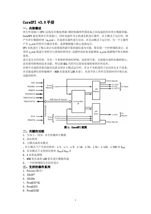
CoreSPI v3.0手册一、内核概述串行外设接口(SPI)总线允许微处理器/微控制器和外围设备之间高速的同步串行数据传输。
CoreSPI能实现串行外设接口,同时也能作为主机或从机进行操作。
在主模式下运行时,核产生串行数据时钟(m_sck),并选择从器件进行访问。
在从动模式下运行时,另一个主器件产生s_sck时钟并且激活从机,选择数据输入核心连接运行。
SPI从机进行了精心设计从而使提供最可靠的通信成为可能。
要实现一个时钟域的设计,必须对s_sck线进行采样并与系统时钟同步。
这额外的好处是能增加s_sck线路噪声和毛刺的宽度。
设计是完全同步的,并有一个系统时钟的时钟域。
这将更可靠,无故障合成和实施的核心。
没有使用特殊的技术功能,所以源HDL代码可以很容易地转移到任何技术。
在核中合成的其他功能还包括支持在主模式运行时,有8个从机线用于访问多达8个设备,并且能选择位的传输顺序(MSB在前或者LSB在前),从而节省工作时宝贵的时间不执行此功能的软件。
图1:CoreSPI框图二、关键的功能1、全双工,同步,8位传输串行数据2、高比特率3、主模式或者从模式4、在主模式下产生的比特率:1/2,1/4,1/8,1/16,1/32,1/64,1/128,1/256对f PCLK5、在从模式下支持的比特率:f PCLK f PCLK/26、8从机选择线7、MSB优先或者LSB优先进行数据传递8、一个时钟域的完全同步设计三、支持的器件系列1、Fusion(融合)2、IGLOO™3、IGLOOe4、ProASIC®3L5、ProASIC36、ProASIC3E四、设备利用率和性能CoreSPI可以在任何Actel的设备上实现。
CoreSPI各种设备的利用率和性能的总结在表1到表3中列出。
用于布局的速度等级如下:IGLOO系列:STD,融合:-2,ProASIC3 / E:-2,ProASIC PLUS®:STD,Axcelerator®:-2,RTAX - S:-1。
APS X Series 12V DC 230V AC 2000W 纯正三尖波形输出无烟气油声电源说
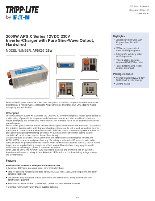
2000W APS X Series 12VDC 230VInverter/Charger with Pure Sine-Wave Output, HardwiredMODEL NUMBER:APSX2012SWPortable 2000W power source for power tools, computers, audio/video components and other sensitive electronics as a vehicle inverter, standalone AC power source or extended-run UPS. Ideal for mobile, emergency and remote sites.DescriptionThe APSX2012SW 2000W APS X Series 12V DC 230V AC Inverter/Charger is a reliable power source for a wide variety of power tools, computers, audio/video components and other sensitive electronics at mobile, emergency and remote sites. With no fumes, fuel or excess noise, it’s an excellent alternative to generator power.The DC-to-AC pure sine-wave inverter delivers network-grade power to sensitive electronics. Its automatic line-to-battery transfer switch and integrated charging system allow the unit to work as a vehicle inverter, standalone AC power source or extended-run UPS. It delivers 2000W of continuous power or 4000W of peak power during equipment startup or cycling. An automatic overload detector, cooling fan and resettable AC circuit breakers protect the unit from damage.Designed for easy installation in RVs, commercial and fleet vehicles and emergency vehicles, theAPSX2012SW converts stored power from any 12V battery or automotive DC source to safe, stable, computer-grade AC power for unlimited runtime. When hardwired to an external 230V AC source, the unit keeps the user-supplied battery charged via a three-stage 6-60A selectable charging system while simultaneously delivering AC power to connected equipment.When used as a UPS, the APSX2012SW responds to blackouts and brownouts with an automatic, instantaneous transfer to battery-derived AC output. LEDs on the unit indicate battery voltage, charger and inverter status.FeaturesReliable Power for Mobile, Emergency and Remote SitesGenerates 230V pure sine-wave power from 12V battery bankqIdeal for powering variable-speed tools, computers, LEDs, fans, audio/video components and other sensitive electronicsqDesigned for easy installation in RVs, commercial and fleet vehicles, emergency vehicles and construction equipmentqFunctions as vehicle inverter, standalone AC power source or extended-run UPSqUnlimited runtime with variety of user-supplied batteriesq HighlightsDelivers pure sine-wave 230VAC power from AC or DCsourceq2000W continuous outputpower; 4000W peak powerqAuto-transfer switching optionfor UPS operationqProtects against blackouts,surges and EMI/RFI line noise qRugged steel housing resistsmoisture and impactqPackage IncludesAPSX2012SW 2000W APS 12V DC 230V AC Inverter/Charger qOwner’s manualqSpecificationsPure Sine-Wave Power for Normal and Peak Power Demands 2000W of continuous powerq 4000W of peak power to accommodate surge power demands during equipment startup and cycling q Automatic overload detector, built-in cooling fan and resettable AC circuit breakers protect unit from damageqHigh-current DC input terminals for simple hardwired installationqAutomatic Transfer SwitchingTransfer relay switches to inverter power during blackout in 10 msq 3-position switch enables Auto, Charge Only or System Off mode q DIP switches configure high and low voltage auto-transferq3-Stage 6-60A Selectable Battery ChargerServes as battery charger when external 230V AC power is supplied and powering connected equipmentq Protects battery from overcharging and overdischarging q Low-battery protection prevents excessive battery depletion q DIP switches configure wet/gel charging profilesqExternal PortsBattery temperature port allows connection of optional remote battery temperature sensor, such as APSSWTEMPq RJ45 communication port allows connection of optional remote control module, such as APSRMSWqFront-Panel LEDsIndicate battery voltage, charger and inverter statusq Rugged Steel HousingResists moisture, vibration and impactq Built-in mounting feet for installation on any rigid horizontal surfaceq© 2023 Eaton. All Rights Reserved. Eaton is a registered trademark. All other trademarks are the property of their respective owners.。
Switching Mode Power Supply 产品说明书

1
SWITCHING MODE POWER SUPPLY SPECIFICATION
E.C.LIST/变更履历表
Rev.
版本
Description of Change/变更内容描述
Before/变更前
After/变更后
01 Original Release(初次发行)
Changed Operator/ Date/日期 执行者
SPECIFICATION FOR APPROVAL
CUSTOMER/客户 :
01097
ARTICLE/品名:
SWITCHING MODE POWER SUPPLY
SPECIFICATION /规格: UL/GS/CE/SAA interchangeable/可换头
MODEL NO/产品型号. : DYS850-240210W-K
2.3 Inrush Current (cold start)/浪涌电流(冷启动) The inrush current will not exceed 80A at 100-240Vac input and Max load for a cold start at 25℃
在 100-240V 交流电输入和最大负载冷启动环境 25℃时浪通电流不能超过 80A
Minimum/最小 Nominal/额定值
Input Voltage/输入电压
90Vac
100Vac~240Vac
Input Frequency/输入频率
47Hz
60Hz/50Hz
Maximum/最大 264Vac 63Hz
2.2 Input AC Current/AC 输入电流
1.3A max @ 100-240Vac input & Full load/在 100 – 240 Vac 输入和满载条件下最大 1.3A 有效值
基于fpga的dpsd算法实现新方法

基于fpga的dpsd算法实现新方法基于fpga的dpsd算法实现新方法基于FPGA的DPSD 算法实现新方法-电气论文基于FPGA的DPSD算法实现新方法汪浩,管国云,陈学英(电子科技大学,四川成都610054)摘要:针对当前测井仪器接收电路多通道、小体积、低功耗、高效率的设计要求,提出了一种基于FPGA的DPSD算法实现新方法。
该方法采用一种简化的正交DPSD处理方法,方便电路和算法的实现;串行ADC采样数据直接进入运算,无需串并转换,在节省FPGA引脚的同时保证了算法效率;用移位累加操作代替乘法操作,极大地降低了算法对FPGA逻辑资源的消耗。
在具体FPGA器件上的实现结果表明,该方法能够在不影响算法效率的情况下减少对FPGA引脚占用和近一半的逻辑资源消耗,满足预先的设计要求。
关键词:测井仪器;DPSD;FPGA资源消耗;串行ADC;移位累加中图分类号:TN402?34 文献标识码:A 文章编号:1004?373X(2015)16?0129?04 收稿日期:2015?03?04 基金项目:国家自然科学基金项目(60931004)0 引言在医疗、军事、测井等诸多领域都需要对微弱信号进行测量[1?3]。
对微弱信号测量的核心问题是在高噪声背景下,当待测信号有可能已被淹没在噪声中时,提取待测信号的幅度、相位等信息。
以电法测井应用为例,测井仪器通常需要通过信号的激励发射、信号在地层中的响应、响应信号的检波接收等3个过程,完成对地层信息的初步采集。
受限于地层响应的固有特性和仪器的发射功率,仪器接收到的响应信号往往十分微弱,有时甚至会低至几nV。
此时,一般的检波方式难以精确提取接收信号中的幅度、相位等信息。
相敏检波利用互相关原理,能够十分有效地从噪声中提取出与参考信号具有相关性的待测信号的幅度和相位信息,同时忽略不相关的背景噪声的干扰[4]。
数字相敏检波(DPSD)通过数字方式实现相敏检波,避免了由乘法器和积分器组成的模拟相敏检波器件的非线性和过载现象[5]。
- 1、下载文档前请自行甄别文档内容的完整性,平台不提供额外的编辑、内容补充、找答案等附加服务。
- 2、"仅部分预览"的文档,不可在线预览部分如存在完整性等问题,可反馈申请退款(可完整预览的文档不适用该条件!)。
- 3、如文档侵犯您的权益,请联系客服反馈,我们会尽快为您处理(人工客服工作时间:9:00-18:30)。
PQ208
PQ208
PQ208
FG144, FG256, FG144, FG256, FG144, FG256,
FG484
FG484
FG484
Notes:
1. Refer to the CoreMP7 datasheet for more information. 2. AES is not available for ARM-enabled ProASIC3 devices. 3. Six chip (main) and three quadrant global networks are available for A3P060 and above. 4. For higher densities and support of additional features, refer to the ProASIC3E Flash FPGAs datasheet. 5. The M7A3P250 device does not support this package.
ProASIC®3 Flash Family FPGAs
with Optional Soft ARM® Support
Product Brief ®
Features and Benefits
High Capacity
• 30 k to 1 Million System Gates • Up to 144 kbits of True Dual-Port SRAM • Up to 300 User I/Os
Reprogrammable Flash Technology
• 130-nm, 7-Layer Metal (6 Copper), Flash-Based CMOS Process
• Live at Power-Up (LAPU) Level 0 Support • Single-Chip Solution • Retains Programmed Design when Powered Off
Advanced I/O
• 700 Mbps DDR, LVDS-Capable I/Os (A3P250 and above) • 1.5 V, 1.8 V, 2.5 V, and 3.3 V Mixed-Voltage Operation • Bank-Selectable I/O Voltages—Up to 4 Banks per Chip • Single-Ended I/O Standards: LVTTL, LVCMOS 3.3 V /
Package
QN132
81
80
84
87
19
–
–
–
–
–
VQ100
77
71
71
68
13
–
–
–
–
–
TQ144
–
91
100
–
–
–
–
–
–
–
–
PQ208
–
–
133
151
34
151
34
154 35
154
35
FG144
–
96
97
97
24
97
25
97
25
97
25
FG256
–
–
–
157
38
178
38
177 43
177
RAM kbits (1,024 bits)
4,608-Bit Blocks
FlashROM Bits Secure (AES) ISP2
Integrated PLL in CCCs VersaNet Globals3
I/O Banks
Maximum User I/Os
Package Pins QFN VQFP TQFP PQFP FBGA
ProASIC3 Devices
ARM®-Enabled ProASIC3 Devices1
A3P030 A3P060 A3P125 A3P250
A3P400
A3P600
A3P1000
M7A3P250 M7A3P400 M7A3P600 M7A3P1000
System Gates
VersaTiles (D-flip-flops)
May 2007 © 2007 Actel Corporation
1 See the Actel website for the latest version of the datasheet.
ProASIC3 Flash Family FPGAs
I/Os Per Package1
ProASIC3 Devices
PP = Pre-Production ES = Engineering Sample (Room Temperature Only)
Capabilities and External Feedback, Multiply/Divide, Delay Capabilities, and External Feedback • Wide Input Frequency Range (1.5 MHz to 350 MHz) • CoreMP7Sd (with debug) and CoreMP7S (without debug
In-System Programming (ISP) and Security
• Secure ISP Using On-Chip 128-Bit Advanced Encryption Standard (AES) Decryption (except A3P030 and ARM®enabled ProASIC®3 devices) via JTAG (IEEE 1532– compliant)
Clock Conditioning Circuit (CCC) and PLL (except A3P030)
• Six CCC Blocks, One with an Integrated PLL • Configurable Phase-Shift, Multiply/Divide, Delay
On-Chip User Nonvolatile Memory
• 1 kbit of FlashROM with Synchronous Interfacing
High Performance
• 350 MHz System Performance • 3.3 V, 66 MHz 64-Bit PCI (except A3P030)
ARM-Enabled ProASIC3 Devices
A3P030 A3P060 A3P125
A3P250 3
A3P400 3
M7A3P250 3, 4 M7A3P400 3 I/O Type
A3P600 M7A3P600
A3P1000 M7A3P1000
Single-Ended I/O Single-Ended I/O Single-Ended I/O Single-Ended I/O2 Differential I/O Pairs Single-Ended I/O2 Differential I/O Pairs Single-Ended I/O2 Differential I/O Pairs Single-Ended I/O2 Differential I/O Pairs
44
FG484
–
––Leabharlann ––194
38
235 60
300
74
Notes:
1. Each used differential I/O pair reduces the number of single-ended I/Os available by two. 2. For A3P250 and A3P400 devices, the maximum number of LVPECL pairs in east and west banks cannot exceed 15. 3. The M7A3P250 device does not support FG256 or QN132 packages. 4. FG256 and FG484 are footprint-compatible packages. 5. "G" indicates RoHS-compliant packages. Refer to "ProASIC3 Ordering Information" on page 3 for the location of the "G" in the part
2.5 V / 1.8 V / 1.5 V, 3.3 V PCI / 3.3 V PCI-X (except A3P030), and LVCMOS 2.5 V / 5.0 V Input • Differential I/O Standards: LVPECL, LVDS, BLVDS, and M-LVDS (A3P250 and above) • I/O Registers on Input, Output, and Enable Paths • Hot-Swappable and Cold Sparing I/Os (A3P030 only) • Programmable Output Slew Rate (except A3P030) and Drive Strength • Weak Pull-Up/Down • IEEE 1149.1 (JTAG) Boundary Scan Test • Pin-Compatible Packages Across the ProASIC3 Family
