Method of reducing harmonic noise in vibroseis operations
反激式开关电源外文翻译
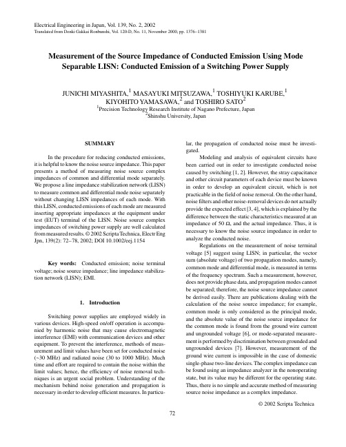
Measurement of the Source Impedance of Conducted Emission Using Mode Separable LISN: Conducted Emission of a Switching Power SupplyJUNICHI MIY ASHITA,1 MASAYUKI MITSUZAW A,1 TOSHIYUKI KARUBE,1KIYOHITO Y AMASAW A,2 and TOSHIRO SA TO21Precision Technology Research Institute of Nagano Prefecture, Japan2Shinshu University, JapanSUMMARYIn the procedure for reducing conducted emissions, it is helpful to know the noise source impedance. This paper presents a method of measuring noise source complex impedances of common and differential mode separately. We propose a line impedance stabilization network (LISN) to measure common and differential mode noise separately without changing LISN impedances of each mode. With this LISN, conducted emissions of each mode are measured inserting appropriate impedances at the equipment under test (EUT) terminal of the LISN. Noise source complex impedances of switching power supply are well calculated from measured results. © 2002 Scripta Technica, Electr Eng Jpn, 139(2): 72 78, 2002; DOI 10.1002/eej.1154Key words:Conducted emission; noise terminal voltage; noise source impedance; line impedance stabiliza-tion network (LISN); EMI.1. IntroductionSwitching power supplies are employed widely in various devices. High-speed on/off operation is accompa-nied by harmonic noise that may cause electromagnetic interference (EMI) with communication devices and other equipment. To prevent the interference, methods of meas-urement and limit values have been set for conducted noise (~30 MHz) and radiated noise (30 to 1000 MHz). Much time and effort are required to contain the noise within the limit values; hence, the efficiency of noise removal tech-niques is an urgent social problem. Understanding of the mechanism behind noise generation and propagation is necessary in order to develop efficient measures. In particu-lar, the propagation of conducted noise must be investi-gated.Modeling and analysis of equivalent circuits have been carried out in order to investigate conducted noise caused by switching [1, 2]. However, the stray capacitance and other circuit parameters of each device must be known in order to develop an equivalent circuit, which is not practicable in the field of noise removal. On the other hand, noise filters and other noise-removal devices do not actually provide the expected effect [3, 4], which is explained by the difference between the static characteristics measured at an impedance of 50 Ω, and the actual impedance. Thus, it is necessary to know the noise source impedance in order to analyze the conducted noise.Regulations on the measurement of noise terminal voltage [5] suggest using LISN; in particular, the vector sum (absolute voltage) of two propagation modes, namely, common mode and differential mode, is measured in terms of the frequency spectrum. Such a measurement, however, does not provide phase data, and propagation modes cannot be separated; therefore, the noise source impedance cannot be derived easily. There are publications dealing with the calculation of the noise source impedance; for example, common mode is only considered as the principal mode, and the absolute value of the noise source impedance for the common mode is found from the ground wire current and ungrounded voltage [6], or mode-separated measure-ment is performed by discrimination between grounded and ungrounded devices [7]. However, measurement of the ground wire current is impossible in the case of domestic single-phase two-line devices. The complex impedance can be found using an impedance analyzer in the nonoperating state, but its value may be different for the operating state. Thus, there is no simple and accurate method of measuring source noise impedance as a complex impedance.© 2002 Scripta TechnicaElectrical Engineering in Japan, V ol. 139, No. 2, 2002Translated from Denki Gakkai Ronbunshi, V ol. 120-D, No. 11, November 2000, pp. 1376 1381The authors assumed that the noise source impedance could be found easily using only a spectrum analyzer, provided that the noise could be measured separately for each mode, and the LISN impedance could be varied. For this purpose, a LISN with a balun transformer was devel-oped to ensure noise measurement, with the common mode and differential mode strictly separated. An appropriate known impedance is inserted at the EUT (equipment under test) terminals, and the noise source impedance is found from the variation of the noise level. This method was used to measure the conducted noise of a switching power sup-ply, and it was confirmed that the noise source impedance could be measured as a complex impedance independently for each mode. Thus, significant information for noiseremoval and propagation mode analysis was acquired.This paper presents a new method of measuring the noise source impedance of conducted emission using mode-separable LISN.2. Separate Measurement for Common Mode andDifferential ModeThe conventional single-phase LISN circuit for measurement of the noise terminal voltage is shown in Fig.1. The power supply is provided with high impedance by a 50-µH reactor, and a meter with an input impedance of 50Ω is connected between one line and the ground via a high-pass capacitor, and another line is terminated by 50 Ω. Thus, the LISN impedance as seen at the EUT is 100 Ω in the differential mode, and 25 Ω in the common mode. The measured value is the vector sum of both modes, and the noise must be found separately in order to find the noise source impedance for each mode. There is LISN with Y-to-delta switching to provide mode separation [8], but its impedance is 150 Ω, giving rise to a problem of data compatibility with 50-Ω LISN. Thus, a new mode-separa-ble LISN was developed as shown in Fig.2. The circuit is identical to that in Fig. 1 from the power supply through the high-pass capacitor. Switching of the connection pattern ensures measurement with one line of the balun transformer terminated by 50 Ω, and another line connected to the meter.In Fig. 2, the secondary side of the 2:1 balun trans-former is terminated by 50 Ω, while the primary side has 200 Ω; in the differential mode, the impedance (line-to-line) is 100 Ω since 200 Ω at the high-pass capacitor is connected in parallel. With the switch set at D, the meter is connected to the secondary side of the balun transformer. The voltage is one-half that of the line-to-line voltage, and measurement is performed in the standard way.The common mode current flows from both sides of the balun transformer via the middle tap to the 50-Ω termi-nal. The currents in the windings are antiphase, and no voltage is generated at the secondary side. Therefore, the impedance of the primary side is the terminal resistance of the tap. Since this impedance is connected in parallel to 50Ω (two 100 Ω in parallel) at the high-pass capacitor, the impedance between the common line and ground is 25 Ω. With the switch set at C, the meter is connected to the middle tap of the balun transformer, and the common-mode voltage is the line-to-ground voltage.3. Measurement of Noise Source Impedance3.1 Measurement circuit and calculationThough the propagation routes are different in the two modes, propagation from the noise source to the LISN can be represented in a simplified way as shown in Fig. 3. In the initial measurement, the load impedance Z L is the LISN impedance. Z L can be varied by inserting a knownimpedance at the EUT terminals. Consider three load im-Fig. 1. Standard 50-Ω/50-µH LISN.Fig. 2.Mode-separable LISN.Fig. 3. Schematic circuit of noise propagation.pedances, namely, LISN only and LISN with two different impedances inserted, Z L 1(R 1 + jX 1), Z L 2(R 2 + jX 2), andZ L 3(R 3+ jX 3). Using the values I 1, I 2, I 3 (scalars) measured in the three cases, Z 0(R 0 + jX 0) is found. Since V 0 = |Z L | × I ,the following expressions can be derived:From the above,Here a , b , and c are as follows:Substituting Eq. (2) into Eq. (1), the following quadratic equation for R 0 is obtained:Thus, R 0 and X 0 have two solutions each. The series of frequency points with positive R 0 is taken as the noise source impedance.3.2 Method of measurementAn impedance is inserted at the EUT terminals in order to measure the noise source impedance in the LISN as seen at the EUT. As shown in Fig. 4, the impedance is inserted so as to vary only the impedance in the mode under consideration, thus preventing an influence on the imped-ance in the other mode. In the diagram, V m is the voltage at the meter connected to the LISN, while the input impedance of the meter (50 Ω) is represented by the parallel resistance.Since parameters of both the LISN and the inserted imped-ance are known, the noise current I can be calculated from V m . Now Z 0 is calculated for each mode from the measured data obtained while varying Z L , by using Eqs. (2) and (3).With the differential mode shown in Fig. 4(a), CR is inserted between the two lines, thus varying the load im-pedance Z L . In the differential mode, Z 0 is assumed to be a low impedance, and hence the inserted impedance exerts a significant effect on the measured value. For this reason, 1Ω/0.47 µF and 0 Ω/0.1 µF were inserted, which are rather small compared to the LISN impedance.The measurement of the common mode shown in Fig.4(b) employs common-mode chokes that basically have no impedance in the differential mode. The common-mode chokes are provided with a secondary winding (ratio 1:1),so that the impedance at the secondary side can be varied.In the common mode, Z 0 is assumed to have a particularly high impedance in the low-frequency band. For this reason,5.1 k Ω and 100 pF were used as the secondary load for the common-mode choke to obtain a high inserted impedance.The measured data for the inserted impedance in the case of resistive and capacitive loads are presented in Fig. 5. The impedance of the common-mode choke includes its own inductance and the secondary load. In the case of a capaci-tive load, the resonance point is around 200 kHz; at higher frequencies, the impedance becomes capacitive.A single-phase two-line switching power supply (an ac adapter for a PC with an input of ac 100 V , a rated power of 45 W, and PWM switching at 73 kHz) was used as the EUT, and the rated load resistance was connected at the dcside. Filters were used for both the common and differential(1)modes, except for the case in which one common-mode choke was removed, in order to obtain the high noise level required for analysis. Both the EUT and the loads had conventional commercial ratings, and were placed 40 cm above a metal ground plate; the power cord was fixed.4. Measurement Results and Discussion The results of conventional measurement as well as common-mode and differential-mode measurement for the LISN without inserted impedance are shown in Fig. 6. The measurements were performed in the range of 150 kHz through 30 MHz, divided into three bands, using a spectrum analyzer with frequency linear sweep. Time-variable data were measured at their highest levels using the Max Hold function of the spectrum analyzer, and only the peak values were employed for calculation of Z 0. For this purpose, the values measured in every frequency band were subjected to the FFT, and all harmonics higher than the fundamental frequency were removed. The data were smoothed, and about 10 peak points were detected in every frequency band. In addition, only those peaks that were stronger than the meter s background noise by at least 6 dB were consid-ered.The results in Figs. 6(b) and 6(c) pertain to the LISN only; the level would vary with inserted impedance. The noise source impedance for both modes calculated from the measured data (using triple measurement) is given in Figs.7 and 9, respectively. The bold and dashed lines pertain to data acquired with the impedance analyzer at the EUT power plug, with the EUT not in operation. With the differ-ential mode, there were no high-frequency components, as shown in Fig. 6(b), and hence the impedance is calculated only for significant low-frequency peaks.The noise source impedance in differential mode can be represented schematically as in Fig. 8. The noise sourceimpedance is equal to the impedance between the LISNFig. 5.Inserted impedance in common mode.Fig. 6. Measured results of standard, differential-mode,and common-mode.Fig. 7. Noise source impedance for differential mode.terminals when the noise source is short-circuited. With switching power supplies, filtering is usually performed by a capacitor of 0.1 to 1 µF inserted between the lines. Since the impedance of the power cord is small in the measured frequency range, one may assume that the impedance as seen at the LISN is low, and that the phase changes from capacitive toward inductive as with the measured static characteristics. However, in the case of the given EUT, a nonlinear resistor was inserted between the power cord and the filter as shown in Fig. 8, and hence the impedance is rather high in the nonoperating state. In addition, there are rectifying diodes on the propagation route, but they do not conduct at the measurement voltage of the impedance ana-lyzer. The noise levels show considerable variation at 120Hz, which corresponds to the on/off frequency of the recti-fying diodes; however, only the peak values are measured and then used for calculation, and hence the impedance obtained by the proposed method is considered to pertain to the conductive state. For this reason, the results do not agree well with static characteristics. Thus, the impedance in the operating state cannot be measured in the differential mode.On the other hand, the measured data for |Z 0| in common mode agree well with the static characteristics, as shown in Fig. 9. The phase, too, exhibits a similar variation,although the scatter is rather large. The resistive part of three load impedances and Z 0 may be presented in a simplified way as in Fig. 10. From Eq. (1), the following is true for R 2,R 3, and Z 0:The distance ratio from Z 0 to R 3 and R 2 on the R X plane that satisfies this equation is I 2:I 3, which corresponds to a circle with radius r as in Eq. (4), with the center lying on the line R 3R 2:Similar circles for R 1 and R 2 are also shown in the diagram.When Z 0 and the load impedances lie on one line, the twocircles have a common point. Equation (4) indicates that if I 3 increases slightly, the outer circle becomes bigger, and the two circles do not adjoin. On the other hand, when the outer circle becomes smaller, the two circles intersect at two points, and X 0 varies more strongly than R 0. In practice, the difference in noise level due to the inserted impedance may drop below 1 dB at some frequencies, so that the solution for Z 0 becomes unavailable because of the scatter, or the phase scatters too much. The measurement accuracy is governed by the difference in noise level, and thus the inserted impedance should have a large enough variation compared to the measurement scatter; in addition, there should be a phase difference so that the two circles are not aligned, as in Fig. 10.Figures 7 and 9 pertain to one of the solutions of Eq.(3) with larger R 0. Here R 0 is not necessarily positive and the other solution is not necessarily negative. The two solutions may be basically discriminated from the fre-quency response and other characteristics, but other inser-tion data are employed for the sake of accuracy.Fig. 8. Equivalent circuit of differential-mode noisesource impedance.(4)Fig. 9.Noise source impedance for common mode.Fig. 10. Load impedances and Z 0 on R X plane.Figure 11 compares the measured data and calculated data for the variation of noise level due to insertion of a commercially available common-mode choke, with the cal-culation based on the results of Fig. 9 and the impedance of the common-mode choke. As is evident, the calculation agrees well with the measured values. On the other hand, a considerable discrepancy was confirmed for the other solu-tion. The noise source impedance found as explained above is accurate enough to predict the filtering effect.The noise source resistance in the common mode can be represented as in Fig. 12. Here Z 1 is the stray capacitance between the internal circuit and the case, and Z 2 is the stray capacitance between the case and the ground plate (or in the case of the ground wire, the impedance of the wire). The common-mode noise source impedance for a single-phase two-line EUT is primarily Z 2, becoming capacitive at low frequencies. Since the EUT is equipped with a filter, the influence of the primary rectifying diodes is not related to common-mode, and hence the data measured by the pro-posed method are very close to the static characteristics.However, this is not necessarily true in the case of a grounded line (Z 2 short-circuited) with no filter installed.In addition, here the full impedance as seen at the LISN is found; in practice, however, a filter or Z 1 is employed to suppress noise. Therefore, the impedance of the power cord is required as well as Z 1 and Z 2 in order to analyze the filtering effect. The impedance of the power cord or grounded wire can be easily determined by measurement or calculation. In our experiments without ground, the impedance is very close to Z 2; on the other hand, Z 1 might be measured by grounding the case and removing the filter (Fig. 12), and then used to analyze the filtering effect between the case and the lines. However, noise propagation in the inner circuit must be further investigated in order to estimate the noise-suppressing efficiency of Z 1.5. ConclusionsA new mode-separable LISN is proposed that sup-ports noise measurement without changing the impedance depending on the mode. The proposed LISN ensures accu-rate measurement for each mode, thus supporting imped-ance analysis.With the proposed LISN, an appropriate impedance is inserted at the EUT terminals, and the noise impedance can be found as a complex impedance, just as simply as with conventional measurement of the noise terminal voltage.The value of the inserted impedance must be chosen prop-erly in order to determine the phase accurately. The pro-posed method ensures sufficient accuracy not only to investigate noise propagation and design efficient counter-measures, but also to predict the filtering effect. The pro-posed technique can supply important data for future analysis of noise generation and propagation in switching power supplies.REFERENCES1.Matsuda H et al. Analysis of common-mode noise in switching power supplies. NEC Tech Rep 1998;51:60 65.2.Ogasawara S et al. Modeling and analysis of high-frequency leak currents generated by voltage-fed PWM inverter. Trans IEE Japan 1995;115-D:77 83.3.Iwasaki M, Ikeda T. Evaluation of noise filters for power supply. Tech Rep IEICE EMCJ 1999;90:1 6.4.Kamita M, Toyama K. A study on attenuation char-acteristics of power filters. Tech Rep IEICE EMCJ 1996;96:45 50.rmation technology equipment Radio distur-bance characteristics Limits and method of meas-urement. CISPR 22, 1997.Fig. 11. V ariation of noise level due to insertion ofanother impedance (measured and calculated data).Fig. 12. Equivalent circuit of common-mode noisesource impedance.6.K amita M, Oka N. Calculation of common-mode noise output impedance during operation. Tech Rep IEICE EMCJ 1998;98:59 65.7.Ran L, Clare C, Bradley K J, Chriistoopoulos C.Measurement of conducted electromagnetic emis-sions in PWM motor drive without the need for an LISN. IEEE Trans EMC 1999;41:50 55.8.Specification for radio disturbance and immunity measuring apparatus and method Part 1: Radio dis-turbance and immunity measuring apparatus. CISPR 16-1, 1993.AUTHORS (from left to right)Junichi Miyashita (member) graduated from Tohoku University in 1981 and joined the Precision Technology Research Institute of Nagano Prefecture. His research interests are EMC measurement and prevention. He is a member of IEICE.Masayuki Mitsuzawa (nonmember) graduated from Nagoya University in 1984 and joined the Precision Technology Research Institute of Nagano Prefecture. His research interests are EMC measurement and prevention. He is a member of JIEP .Toshiyuki Karube (nonmember) graduated from Waseda University in 1991 and joined the Precision Technology Research Institute of Nagano Prefecture. His research interests are EMC measurement and prevention. He is a member of IEICE and JIEP .Kiyohito Yamasawa (member) completed the M.E. program at Tohoku University in 1970. He has been a professor at Shinshu University since 1993. His research interests are magnetic device integration, microswitching power units, and microwave sensors. He holds a D.Eng. degree and is a member of IEICE, SICE, the Magnetics Society of Japan, the Japan AEM Society, and IEEE.Toshiro Sato (member) completed his doctorate at Chiba University in 1989 and joined Toshiba Research Institute. He has been an associate professor at Shinshu University since 1996. His research interests are magnetic thin-film devices. He received a 1994 IEE Japan Paper Award and a 1999 Japan Society of Applied Magnetism Paper Award. He holds a D.Sc. degree,and is a member of IEE Japan, IEICE, and the Magnetics Society of Japan.。
调速永磁同步电动机高频电磁噪音的分析与抑制
调速永磁同步电动机高频电磁噪音的分析与抑制(已处理)调速永磁同步电动机高频电磁噪音的分析与抑制Analysis and Simulation of High-FrequencyNoise of Vector-Contorlled PMSM system 调速永磁同步电动机高频电磁噪音的分析与抑制撰稿人:梁文毅5摘要 :可以转化为对高次谐波电流产生的径向力波的分析,从而转化为对 PWM 信号产生高频电流谐波的分析。
本文分析了矢量控制调速永磁同步电动机驱动系统中产目前永磁同步电动机矢量控制通常采用 d-q 轴数学模生 PWM 谐波电流的原因,并基于此分析结果给出了高频型,本节利用该数学模型对 d-q 轴谐波电流进行分析。
电机电磁噪音的特征。
基于分析结果,本文提出了解决该类电磁控制算法采用 SVPWM 控制,调制频率为 fPWM。
噪音的几种方式,并采用有限元仿真软件 EasiMotor 对分析结论进行仿真验证,仿真结果验证了理论分析的正确性。
1.1. 永磁同步电动机 d-q 轴谐波电流分析 [14] 关键词:永磁同步电动机、矢量控制、电磁噪音、PWM谐波电流在文献 [14] 中对 PWM 谐波电流进行了详细分析,根据分析可知,通常情况下,d 轴谐波电流主要为一次 PWMAbstract:谐波电流,其大小与Δid1 直接相关,其中:1?i ?UT cos2αδ 60 ? cos60 ?δ 2 3Ld1 ss dThe high frequency electromagnetic noise causedby PWM has beenanalysed in this paper based on当α 30 +δ/2 时,Δid1 取最大值,其值为:the analysis of the PWM harmonic current in vector- controlled PMSM system. Based on this result, the2 ? i UT 1? cos60? δ 2 3L d1 ss dcharacteristic of the noise has been studied, also some of methodsto reducing the noise has been proposed 这里,Ld 为 d 轴同步电感,δ为功角, Ts 为调制周期,and the simulation of finite element method in Us 为稳态运行时电压矢量幅值, 为电压矢量在扇区中瞬EasiMotor software verified the validity of methods. αKey words: PMSM, Vector Control, Electromagnetic α时位置,0 。
QSC SB-5218和SB-7218双18英寸低音炮用户手册说明书

1*TD-000150-Cinema Loudspeaker Systems User ManualSB-5218 and SB-7218 Dual-18” SubwoofersIntroductionThe SB-5218 and SB-7218 are specially designed cinema subwoofers, featuring dual 500 and 700 watt, respectively, 18” (460mm) low-frequency transducers mounted in ported enclosures. The enclosures are tuned to 25 hertz and use a B6 alignment. These should be used with the B6 boost filter option provided by the QSC SF-1 or SF-3 Subwoofer Filter mod-ules or the QSC Digital Cinema Monitor to ensure extended response to the lowest audible frequencies.Meeting cinema requirements for the extended low frequency response differentiates the SB-5218 and SB-7218 from more conventional “rock-and-roll” subwoofer systems. Their fre-quency range extends to below 25 hertz when used with the correct B6 filter.The two custom 500 watt (700 watt, SB-7218), 18” transducers were developed especially for cinema use. The woofers feature 4” (100mm) voice coils and vented pole pieces to ensure cool operation, even at high power levels. Cooler temperatures increase driver lifespan and decrease problematic power compression at high drive levels. Undercut pole pieces provides a Symmetrical Magnetic Gap (SMG), reducing second harmonic distortion.Enclosures are constructed of high quality MDF panels and feature Single Woofer Chambers (SWC). The separate chamber for each transducer makes the enclosure stronger, provides rigidity, and prevents cone over-excursion in the rare event of a driver failure (enclosure “loading” is not lost for the remaining transducer).Large, Fully Radiused Ports (FRP) ensure smooth air flow through the ports, especially at higher drive levels. This prevents potentially audible port turbulence noise. Both internal and external port openings are fully radiused.With Symmetrical Port Loading (SPL) bass ports are evenly spaced on each side of the trans-ducers, making internal pressure more uniform across the back surface of the transducer. This prevents the cone from being displaced to one side or another by unbalanced air pres-sure, reducing the chance of driving the voice coil out of the center of the gap at high drive levels.Enclosure is not designed to be suspended, flown, or rigged. Do not sus-pend, fly, or rig this enclosure.This product is capable of producing sound pressure levels that can perma-nently damage human hearing. Always keep sound pressure levels in the listening area below levels that can damage human hearing.Install in accordance with QSC Audio Product’s instructions and alicensed, professional engineer. Only use attachments, mounts, accesso-ries, or brackets specified by QSC Audio Products, Inc. Refer all servicing to qualified personnel. Servicing is required when the apparatus has been damaged in any way.WARNING! Before placing, installing, rigging, or suspending any speaker product, inspect all hardware, suspension, cabinets, transducers, brackets and associated equipment for damage. Any missing, corroded, deformed or non-load rated component could significantly reduce the strength of the installation, placement, or array. Any such condition severely reduces the safety of the installation and should be immediately corrected. Use only hardware which is rated for the loading conditions of the installation and any possible short-term unexpected overloading. Never exceed the rating of the hardware or equipment. Consult a licensed, professional engineer when any doubt or questions arise regarding a physical equipment installa-tion.TD-000150-00 rev.C© Copyright 2003, 2004, QSC Audio Products, Inc.QSC® is a registered trademark of QSC Audio Products, Inc.“QSC” and the QSC logo are registered with the U.S. Patent and Trademark Office1675 MacArthur Blvd., Costa Mesa, CA, 92626 USAMain Number (714) 754-6175 Sales & Marketing (714) 957-7100 or toll free (USA only) (800) 854-4079Customer Service(714) 957-7150 or toll free (USA only) (800) 772-28342ConnectionsNormal Connection The SB-5218/7218 has barrier strip screw ter-minals for connection. The terminals accept up to #10 AWG stranded loudspeaker wiring. Use the largest wire size and shortest wire length possible for a given installation. Observe the polarity markings and keep polarity consistent throughout the system for best performance.Parallel Connection of Second SB-5218/7218The terminals marker SPK2 may be used to con-nect another SB-5218/7218 in parallel. Connect the wires as shown in the illustration, at right. Note: If the SB-5218/7218’s internal wiring has been modified in any way, this may not func-tion. If this is the case, remove the terminal cup and verify the presence of the factory yellow jumper and blue jumper wires; remedy as required or have the loudspeaker serviced.Individual Transducer Connection (requires modification)The transducers are wired in parallel inside the enclosure. If individual transducer connection is required, remove the terminal cup and remove the yellow and the blue jumper wires that are connected between the SPK1 and SPK2 termi-nals. Replace the terminal cup and mark the enclosure with a note of the modification.Normal Connection Example:Parallel Connection Example:Individual TransducerConnection Example:3Specifications (subject to change without notice)SB-5218SB-7218Frequency Range:24 - 100 Hz (±3 dB)22 - 100 Hertz (±3 dB)19 - 250 Hz useable range (-10 dB)19 - 250 Hertz useable range (-10 dB)Maximum Output:135 dB SPL calculated peak137 dB SPL calculated peak1 meter, half space, at rated rms power with 6 dB crest factor pink noise input, 25 - 250 Hertz.129 dBA SPL calculated maximum continuous 130.5 dBA SPL calculated maximum continuous1 meter. The dBA scale is typically used to identify sound sources which can cause permanent hearing loss.Impedance:4 ohms, nom. (3.2 @ 25 Hz., 62 @ 50 Hz.) 4 ohms, nom. (3.2 @ 27 Hz., 28 @ 48 Hz.)Maximum Input Power:100 hours of 6 dB crest factor 800 watts rms1200 watts rmspink noise, 25 - 250 Hertz2 hours of 6 dB crest factor1000 watts rms1500 watts rmspink noise, 25 - 250 Hertz, AES methodRecommended Amp Power:1600 watts rms maximum 2600 watts rms maximum Sensitivity:99.5 dB half space 101.0 dB half space (25 - 100 Hz, 1 watt, 1 m.)93.5 dB full space95.0 dB full spaceWeight:225 lbs. shipping, 205 lbs. net (102/93 kg.)230 lbs. shipping, 210 lbs. net (104/95 kg.)Both Models-Nominal Coverage:Omnidirectional (80 Hz)Recommended Processing:LF boost- freq.= 25 Hz, Q=2.0, gain= +6 dB. QSC DSP configurations are available at . Parameters for alternative processing hardware are available upon request.Connectors:Barrier strip screw terminals accept up to #10 AWG stranded wire. Four terminals: (two INPUT and two PARALLEL OUT). Drivers are internally wired in parallel. For independent transducer connection, remove blue jumper wire and yellow jumper wire on internal-side of terminal cup and mark enclosure accordingly.Transducers:Two 18” (457mm) high efficiency subwoofer transducers featuring vented 4” (100mm) copper voice coils on Kapton® formers. High excursion/low distortion design, with extremely high power handling, and low thermal and port com-pression.Enclosure:B6 alignment, vented enclosure with symmetrical port design, tuned to 25 Hz, constructed of medium density fibre-board and heavily braced. Features vandal resistant woofer mounting bolts.Size:30” wide X 48” high X 24” deep (762 mm X 1220 mm X 610 mm)4Warranty (USA only; other countries, see your dealer or distributor)DisclaimerQSC Audio Products, Inc. is not liable for any damage to amplifiers, or any other equipment that is caused by negligence or improper installation and/or use of this loudspeaker product. QSC Audio Products 3 Year Limited WarrantyQSC Audio Products, Inc. (“QSC”) guarantees its products to be free from defective material and / or workmanship for a period of three (3) years from date of sale, and will replace defective parts and repair malfunctioning products under this warranty when the defect occurs under normal installation and use - provided the unit is returned to our factory or one of our authorized service stations via pre-paid transportation with a copy of proof of purchase (i.e., sales receipt).This warranty provides that the examination of the return product must indicate, in our judgment, a manufacturing defect.This warranty does not extend to any product which has been subjected to misuse, neglect, accident, improper installation, or where the date code has been removed or defaced. QSC shall not be liable for incidental and/or consequential damages.This warranty gives you specific legal rights. This limited warranty is freely transferable during the term of the warranty period.Customer may have additional rights, which vary from state to state.In the event that this product was manufactured for export and sale outside of the United States or its territories, then this lim-ited warranty shall not apply. Removal of the serial number on this product, or purchase of this product from an unauthorized dealer, will void this limited warranty. Periodically, this warranty is updated. To obtain the most recent version of QSC’s war-ranty statement, please visit . Contact us at 800-854-4079 or visit our website at .Contacting QSC Audio ProductsMailing address:QSC Audio Products, Inc.1675 MacArthur BoulevardCosta Mesa, CA 92626-1468 USATelephone Numbers:Main Number (714) 754-6175Sales & Marketing (714) 957-7100 or toll free (USA only) (800) 854-4079Customer Service(714) 957-7150 or toll free (USA only) (800) 772-2834Facsimile Numbers:Sales & Marketing Fax(714) 754-6174Customer Service Fax(714) 754-6173World Wide Web: E-mail:*************************************QSC Audio Products, Inc. 1675 MacArthur Boulevard Costa Mesa, California 92626 USA ©2003, 2004 “QSC” and the QSC logo are registered with the U.S. Patent and Trademark Office.Kapton® is a registered trademark of E.I. du Pont de Nemours and Company.5Manual del usuario de los sistemas de altavoces para salas de cineSubwoofers dobles de 18"SB-5218 y SB-7218IntroducciónLos subwoofers SB-5218 y SB-7218 están especialmente diseñados para salas de cine, cuentan con dos transductores de baja frecuencia de 18” (460mm), de 500 y de 700 vatios,respectivamente, montados en cajas con puertos. Las cajas están afinadas a 25 hertz y usan una alineación B6. Deben usarse con la opción de filtro intensificador B6 proporcionada por los módulos de filtro de subwoofer QSC SF-1 o SF-3 o por el monitor de cine digital QSC para asegurar la respuesta extendida a las frecuencias audibles más bajas.El cumplimiento de los requisitos de salas de cine respecto a la respuesta extendida de baja frecuencia distingue a los subwoofers SB-5218 y SB-7218 de los sistemas de subwoofers tipo “rock-and-roll” más convencionales. Su intervalo de frecuencia se extiende por debajo de los 25 hertz cuando se usan con el filtro B6 correcto.Los dos transductores de 18", de 500 vatios (700 vatios para el SB-7218) se desarrollaronespecíficamente para su uso en salas de cine. Los woofers tienen bobinas de voz de 4” (100 mm) y polos ventilados para asegurar una operación fría, incluso a niveles de alta potencia. Lastemperaturas más frías aumentan la vida útil del excitador y reducen la problemática compresión de la potencia a niveles altos de excitación. El polo proyectado proporciona un campo magnético simétrico (Symmetrical Magnetic Gap, SMG), reduciendo la segunda deformación armós cajas están construidas con paneles MDF (cartón duro de densidad media) y tienen cámaras de woofer sencillo (Woofer Chambers, SWC). La cámara separada para cada transductorproporciona a la caja resistencia, rigidez, y evita la excursión excesiva del cono en el raro evento de una falla del excitador (la "carga" de la caja no se pierde para el transductor restante).Los grandes puertos totalmente redondeados (Fully Radiused Ports, FRP) aseguran un flujo de aire uniforme a su través, especialmente a niveles mayores de excitación. Esto evita ruido de turbulencia en el puerto potencialmente audible. Ambas aberturas del puerto, la interna y la externa, están totalmente redondeadas.Con la carga simétrica de los puertos (Symmetrical Port Loading, SPL), los puertos de bajos están igualmente separados a cada lado de los transductores, haciendo que la presión interna sea más uniforme a través de la superficie posterior del transductor. Esto evita que el cono sea desplazado de un lado a otro por la presión no equilibrada del aire, reduciendo la probabilidad de impulsar la bobina de voz fuera del centro del espacio a altos niveles de excitación.La caja no está diseñada para montarse suspendida, en voladizo ni sobre arneses. No suspenda esta caja, no la monte en voladizo ni sobre arneses.Este producto es capaz de producir niveles de presión del sonido que pueden causar daños permanentes al oído humano. Siempre mantenga los niveles de presión del sonido en un área de audición con un nivel menor que el que provoca daños al oído humano.Instale de acuerdo con las instrucciones de QSC Audio Products y de un ingeniero profesional con la debida licencia. Sólo use piezas, montajes,accesorios y soportes especificados por QSC Audio Products, Inc. Refiera todo el servicio a personal calificado. Cuando el aparato haya sido dañado de alguna manera, es necesario proporcionarle servicio.¡ADVERTENCIA! Antes de colocar, instalar, montar o suspender cualquier producto de altavoz, inspeccione todo el herraje, la suspensión, los armarios, los transductores, los soportes y el equipo asociado para detectar laexistencia de daños. Cualquier componente faltante, corroído, deformado, o sin carga nominal podría reducir significativamente la resistencia de lainstalación, la colocación o la configuración. Cualquier condición de este tipo reduce gravemente la seguridad de la instalación y debe corregirse deinmediato. Use sólo herraje que esté clasificado para las condiciones de carga de la instalación y cualquier carga excesiva a corto plazo inesperada posible. Nunca exceda el valor nominal del herraje ni del dispositivo. Consulte a un ingeniero profesional con la debida licencia cuando surjan dudas o preguntas referentes a la instalación física del equipo.*TD-000150-TD-000150-00 rev.C© Derechos de autor 2003, 2004, QSC Audio Products, Inc.QSC® es una marca comercial registrada de QSC Audio Products, Inc.“QSC” y el logotipo de QSC están registrados con la Oficina de Patentes y MarcasComerciales de los Estados Unidos1675 MacArthur Blvd., Costa Mesa, CA, 92626 EE.UU.Número principal +1 (714) 754-6175 Ventas y Comercialización +1 (714) 957-7100 o línea sin costo (sólo para EE.UU.) +1 (800) 854-4079Servicio al cliente +1 (714) 957-7150 o línea sin costo (sólo en EE.UU.) +1 (800) 772-28346ConexionesConexión normalEl SB-5218/7218 tiene terminales de tornillo de barra protectora para su conexión. Losterminales aceptan cableado trenzado de hasta #10 AWG para altavoces. Use el alambre del calibre más grande y de la longitud más corta posible en cualquier instalación. Observe las marcas de polaridad y mantenga la polaridad uniforme en todo el sistema para permitir el mejor rendimiento.Conexión en paralelo de un segundo SB-5218/7218Los terminales marcadores SPK2 se pueden usar para conectar en paralelo otro SB-5218/7218. Conecte los cables como se como se muestra en la ilustración, a la derecha. Nota: si el cableado interno de SB-5218/7218 se ha modificado de alguna manera, es posible que no funcione. En este caso, quite la cúpula del terminal y verifique la presencia de alambres amarillos y azules de puentes instalados en fábrica; corrija el problema según se requiera, o solicite que den servicio al altavoz.Conexión del transductor individual(requiere modificación)Los transductores están conectados en paralelo dentro de la caja. Si se requiere la conexión del transductor individual, quite la cúpula del terminal y quite los alambres amarillo y azul del puente que están conectados entre los terminales SPK1 y SPK2. Vuelva a colocar la cúpula del terminal y marque la caja con una nota que indique la modificación.transductor individual:Ejemplo de una conexión normal:Ejemplo de conexiónen paralelo:7Especificaciones (sujetas a cambio sin previo aviso).SB-5218SB-7218Intervalo de frecuencia:24 - 100 Hz (±3 dB)22 - 100 Hertz (±3 dB)Intervalo útil de 19 - 250 Hz (-10 dB)Intervalo útil de 19 - 250 Hertz (-10 dB)Salida máxima:Pico calculado de SPL: 35 dBPico calculado de SPL: 137 dB1 metro, medio espacio, a una potencia rms nominal con entrada de ruido rosa con factor de cresta de 6 dB, 25 - 250 Hertz.Máximo calculado continuo de SPL: 129 dBA Máximo calculado continuo de SPL: 130.5 dBA1 metro. La escala de dBA típicamente se usa para identificar fuentes de sonido que pueden causar pérdida auditiva permanenteImpedancia:4 ohms, nom. (3.2 a 25 Hz., 62 a 50 Hz.) 4 ohmios, nom. (3.2 a 27 Hz., 28 a 48 Hz.)Potencia máxima de entrada:100 horas de factor de cresta de 6 dB 800 vatios rms 1200 vatios rmsruido rosa, 25 - 250 Hertz2 horas de factor de cresta de 6 dB 1000 vatios rms 1500 vatios rmsruido rosa, 25 - 250 Hertz, método AESPotencia de amperaje recomendada:1600 vatios rms como máximo 2600 vatios rms como máximo Sensibilidad:99.5 dB medio espacio 101.0 dB medio espacio (25 - 100 Hz, 1 vatio, 1 m.)93.5 dB espacio completo95.0 dB espacio completoPeso:225 libras envío, 205 libras neto (102/93 kg.)230 libras envío, 210 libras neto (104/95 kg.)Ambos modelos:Cobertura nominal:Omnidireccional (80 Hz)Procesamiento recomendado:Intensificador de baja frecuencia- frec.= 25 Hz, Q=2.0, ganancia +6 dB. Las configuraciones DSP de QSC estándisponibles en . Los parámetros para el herraje de procesamiento alternativo están disponibles si así se solicitan.Conectadores:Los terminales de tornillo de barra protectora aceptan alambre trenzado de hasta #10 AWG . Cuatro terminales: (dos de ENTRADA y dos de SALIDA PARALELA). Los excitadores están cableados internamente en paralelo. Para la conexión de un transductor independiente, quite los alambres azul y amarillo de los puentes que se encuentran en el lado interno de la cúpula del terminal y marque la caja de acuerdo con esto.Transductores:Dos transductores de subwoofer, de alta eficiencia, de 18” (457mm), con bobinas de voz de cobre de 4” (100mm) ventiladas, en soportes de Kapton®. Diseño de alta excursión/baja deformación, con un manejo de potencia extremadamente alta, y baja compresión térmica y de puerto.Caja:Alineación B6, caja ventilada con diseño de puertos simétricos, afinada a 25 Hz, construida con cartón duro de media densidad y fuertemente soportado. Tiene pernos de montaje del woofer resistentes al vandalismo.Tamaño:30” de ancho X 48” de alto X 24” de profundidad (762 mm X 1220 mm X 610 mm)8Garantía (sólo en EE.UU.; en otros países, consulte a su concesionario o distribuidor)RenunciaQSC Audio Products, Inc. no es responsable por ningún daño a los amplificadores, ni a ningún otro equipo que sea causado por negligencia o instalación y/o uso inadecuado de este altavoz. Garantía limitada de 3 años de QSC Audio ProductsQSC Audio Products, Inc. (“QSC”) garantiza que sus productos estarán libres de materiales y/o mano de obra defectuosos por un periodo de tres (3) años a partir de la fecha de la venta, y reemplazará las piezas defectuosas y reparará los productos que funcionen mal bajo esta garantía cuando el defecto ocurra bajo condiciones normales de instalación y uso, siempre y cuando la unidad se devuelva a nuestra fábrica o a una de nuestras estaciones autorizadas de servicio mediante transportación prepagada con una copia del comprobante de compra (por ejemplo, el recibo de la compra).Esta garantía requiere que el examen del producto devuelto indique, en nuestra opinión, un defecto de fabricación.Esta garantía no se extiende a ningún producto que hubiera estado sometido a uso indebido, negligencia, accidente, instalación incorrecta, o en el que se hubiera quitado o modificado el código de la fecha. QSC tampoco será responsable por daños incidentales y/o emergentes.Esta garantía le otorga derechos legales específicos. Esta garantía limitada es libremente transferible durante el período de la misma.El cliente podría gozar de derechos adicionales, que podrían variar de un estado a otro.En caso de que este producto fuera fabricado para exportación y venta fuera de los Estados Unidos o sus territorios, entonces no será aplicable esta garantía limitada. La eliminación del número de serie en este producto, o la compra de este producto de un distribuidor no autorizado, anularán esta garantía limitada. Esta garantía se actualiza periódicamente. Para obtener la versión más reciente de la declaración de garantía de QSC, visite . Comuníquese con nosotros llamando al 800-854-4079 o visite nuestro sitio en Internet en .Cómo comunicarse con QSC Audio ProductsDirección postal:QSC Audio Products, Inc.1675 MacArthur BoulevardCosta Mesa, CA 92626-1468 EE.UU.Números de teléfono:Número principal +1 (714) 754-6175Ventas y Comercialización +1 (714) 957-7100 o número sin costo (sólo EE.UU.) +1 (800) 854-4079Servicio al cliente +1 (714) 957-7150 o línea sin costo (sólo en EE.UU.) +1 (800) 772-2834Números de fax:Ventas y Comercialización Fax +1 (714) 754-6174Servicio al Cliente Fax +1 (714) 754-6173World Wide Web: Direcciónelectrónica:*************************************QSC Audio Products, Inc. 1675 MacArthur Boulevard Costa Mesa, California 92626 EE.UU.“QSC” y el logo QSC están registrados con la Oficina de Patentes y Marcas Comerciales de EE.UU.Kapton® es una marca comercial registrada de E.I. du Pont de Nemours and Company.9Manuel d'utilisation de systèmes de haut-parleurs de cinéma Doubles caisson d'extrêmes graves de 45,7cmSB-5218 etSB-7218IntroductionLes modèles SB-5218 et SB-7218 sont des caissons d'extrêmes graves spécialement conçus à partir de deux transducteurs basse fréquence de 460mm de 500 et 700W, respectivement enfermés dans des enceintes résonnantes. Les enceintes sont réglées à 25Hz et utilisent un alignement B6. Elles doivent être utilisées avec le filtre d'appoint B6 proposé avec les modules de filtres de caissons d'extrêmes graves QSC SF-1 ou SF-3 ou le moniteur de cinéma numérique QSC pour garantir une réponse étendue aux plus basses fréquences audibles.La satisfaction des exigences des salles de cinéma en matière de réponse basse fréquence étendue différencie les modèles SB-5218 et SB-7218 des systèmes de caissons d'extrêmes graves du type «rock-and-roll », plus conventionnels. Leur plage de fréquence atteint moins de 25 Hz lorsqu'ils sont utilisés avec le filtre B6 correct.Les deux transducteurs personnalisés de 45,7cm/500 W (700 W pour le modèle SB-7218) ont été spécialement développés pour les salles de cinéma. Les caissons d'extrêmes graves ont des bobines mobiles de 100mm et des sections de pôle à évents pour éviter la surchauffe, même à grande puissance. Les basses températures augmentent la durée de vie de l'étage d'attaque et diminuent la compression de puissance problématique à grande puissance. Les sections de pôle évidées assurent un espace magnétique symétrique (SMG), ce qui réduit la distorsion harmonique secondaire.Les enceintes sont faites de panneaux de MDF de haute qualité et ont des compartiments indépendants pour caissons d'extrêmes graves (SWC). Le compartiment séparé pour chaque transducteur rend l'enceinte plus solide, procure une certaine rigidité et empêche ledépassement de course du cône dans l'éventualité rarissime d'une panne d'étage d'attaque (le «chargement » de l'enceinte n'est pas interrompu pour l'autre transducteur).Les grands ports entièrement arrondis (FRP) garantissent la circulation d'air uniforme à travers les ports, surtout à haute puissance. Ceci empêche les interférences sonores. Les ouvertures internes et externes des ports sont entièrement arrondies.Grâce au chargement symétrique des ports (SPL), les ports à graves sont équidistants de part et d'autre des transducteurs, ce qui répartit uniformément la pression interne à travers la surface arrière du transducteur. Ceci empêche le déplacement du cône d'un côté ou de l'autre par un déséquilibre de la pression d'air, ce qui réduit le risque d'excentrage de la bobine mobile à haute puissance.L'enceinte n'a pas été conçue pour être suspendue, balancée ou montée. La suspension , le balancement ou le montage de l'enceinte sont interdits.Ce produit est capable de produire des niveaux de pression sonoresusceptibles d'endommager l'ouïe de manière irréversible. Toujours maintenir les niveaux de pression sonore dans la zone d'écoute en deçà de niveaux susceptibles de compromettre l'ouïe.Installer conformément aux instructions de QSC Audio Products et d’untechnicien professionnel diplômé. Utiliser uniquement des fixations, supports, accessoires ou équerres spécifiés par QSC Audio Products. Confier toutes les réparations à un personnel qualifié. Une réparation ou maintenance est requise lorsque l’appareil a été endommagé d’une manière quelconque.AVERTISSEMENT ! Avant de placer, installer, monter ou suspendre un haut-parleur, inspecter l’état de toute la visserie, du matériel de suspension, des armoires, des transducteurs, des supports et du matériel associé. Toutcomposant manquant, corrodé, déformé ou non adapté à la charge risque de réduire sensiblement la solidité de l’installation, sa mise en place ou sa portée. Une telle condition réduit sensiblement la sécurité de l’installation et doit être immédiatement corrigée. Utiliser uniquement du matériel de montage prévu pour les conditions de charge de l’installation et toute surcharge éventuelle à court terme imprévue. Ne jamais dépasser les spécifications nominales du matériel de montage ou de l’équipement. Consulter un technicienprofessionnel diplômé en cas de doute ou de question concernant l’installation physique de l’équipement.*TD-000150-TD-000150-00 rév. C© Copyright 2003, 2004, QSC Audio Products, Inc.QSC® est une marque déposée de QSC Audio Products, Inc.QSC et le logo QSC sont des marques déposées auprès de l'U.S. Patent andTrademark Office.1675 MacArthur Blvd., Costa Mesa, CA 92626Téléphone (standard)+1 (714) 754-6175 Ventes et Marketing +1 (714) 957-7100 ou +1 (800) 854-4079 (numéro vert valable aux États-Unis seulement)Service clientèle +1 (714) 957-7150 ou numéro vert (États-Unis seulement) +1 (800) 772-2834。
迪米(思瑞浦)2017-9-23贴片运放TP1542A-双路(SOIC-8)-思瑞浦-RoHS 承认报告 第一次送样(黄灼)合格
广东华美骏达电器有限公司材料样品报告供 应H M J D-Q R-02.33A/2标识:3PEAK 1542A BCFe附图1 附图2附图3附图4在输入端输入方波信号,测量输出端的信号波形。
3PEAK1TP1541A/ TP1541NA/TP1542A/TP1544AStable 1.3MHz, Precision, RRIO, Op Amps Rev. B.04Features⏹ Stable 1.3MHz GBWP Over Temperature Range ⏹ Stable 1.3MHz GBWP in V CM from 0V to V DD ⏹ 0.7V/μs Slew Rate⏹ Only 80μA of Supply Current per Amplifier ⏹ Excellent EMIRR: 80dB(1GHz) ⏹ Offset Voltage: 400uV Maximum⏹ Offset Voltage Temperature Drift: 1uV/°C ⏹ Input Bias Current: 1pA Typical⏹ THD+Noise: -105dB at 1kHz, -90dB at 10kHz ⏹ High CMRR/PSRR: 95dB/90dB⏹ Beyond the Rails Input Common-Mode Range ⏹ High Output Current: 100mA⏹ No Phase Reversal for Overdriven Inputs ⏹ Drives 2kΩ Resistive Loads⏹ Shutdown Current: 0.2μA (TP1541NA) ⏹ Single +2.1V to +6.0V Supply Voltage Range ⏹ –40°C to 125°C Operation Temperature Range ⏹ ESD Rating:Robust 8KV – HBM, 2KV – CDM and 500V – MM ⏹Green, Popular Type PackageApplications⏹ Audio Output⏹ Active Filters, ASIC Input or Output Amplifier ⏹ Portable Instruments and Mobile Equipment ⏹ Battery or Solar Powered Systems ⏹ Smoke/Gas/Environment Sensors ⏹ Piezo Electrical Transducer Amplifier ⏹ Medical Equipment ⏹PCMCIA CardsDescriptionTP154xA series are CMOS single/dual/quad op-amps with low offset, stable high frequency response, low power, low supply voltage, and rail-to-rail inputs and outputs. They incorporate 3PEAK ‟s proprietary and patented design techniques to achieve best in-class performance among all micro-power CMOS amplifiers in its power class. The TP154xA family can be used as plug-in replacements for many commercially available op-amps to reduce power and improve input/output range and performance.TP154xA are unity gain stable with Any Capacitive load with a constant 1.3MHz GBWP, 0.7V/μs slew rate while consuming only 80μA of quiescent current per amplifier. Analog trim and calibration routine reduce input offset voltage to below 0.4mV, and proprietary precision temperature compensation technique makes offset voltage temperature drift at 1μV/°C. Adaptive biasing and dynamic compensation enables the TP154xA to achieve …THD+Noise ‟ for 1kHz/10kHz 2V PP signal at -105dB and -90dB, respectively. Beyond the rails input and rail-to-rail output characteristics allow the full power-supply voltage to be used for signal range. This combination of features makes the TP154xA ideal choices for battery-powered applications because they minimize errors due to power supply voltage variations over the lifetime of the battery and maintain high CMRR even for a rail-to-rail input op-amp. General audio output, remote battery- powered sensors, and smoke detector can benefit from the features of the TP154xA op-amps. For applications that require power-down, the TP1541NA in popular type packages has alow-power shutdown mode that reduces supply current to 0.2μA , and forces the output into a high-impedance state.3PEAK and the 3PEAK logo are registered trademarks of 3PEAK INCORPORATED. All other trademarks are the property of their respective owners.Pin Configuration (Top View)TP1541A5-Pin SOT23/SC70Out +In﹣Vs VsTP1542A8-Pin SOIC/TSSOP/MSOPOut A ﹢In A ﹣In A In BIn BOut B﹣VsVs TP1544A14-Pin SOIC/TSSOP﹢﹣In D In D ﹢﹣In C In CVs ﹢TP1541NA6-Pin SC70-V Out A﹢In A ﹣In A ﹣VsIn BIn B Vs TP1542A8-Pin DFN (-F Suffix)黄灼数字签名人 黄灼DN :cn=黄灼,c=CN-中国,o=华美骏达,ou=研发中心原因:我已审阅该文档日期:2017.02.1409:41:49 +08'00'2TP1541A/TP1541NA/TP1542A/TP1544AStable 1.3MHz, Precision, RRIO, Op AmpsRev. B.04 Absolute Maximum Ratings Note 1Supply Voltage: V +– V –....................................7.0V Input Voltage............................. V –– 0.3 to V ++ 0.3 Input Current: +IN, –IN, SHDN Note 2.............. ±10mA Differential Input Voltage................................ ±7VSHDN Pin Voltage ……………………………V – to V +Output Short-Circuit Duration Note 3…............ Infinite Operating Temperature Range.......–40°C to 125°C Maximum Junction Temperature................... 150°C Storage Temperature Range.......... –65°C to 150°C Lead Temperature (Soldering, 10 sec) ......... 260°CNote 1: Stresses beyond those listed under Absolute Maximum Ratings may cause permanent damage to the device. Exposure to anyAbsolute Maximum Rating condition for extended periods may affect device reliability and lifetime.Note 2: The inputs are protected by ESD protection diodes to each power supply. If the input extends more than 500mV beyond the power supply, the input current should be limited to less than 10mA.Note 3: A heat sink may be required to keep the junction temperature below the absolute maximum. This depends on the power supply voltage and how many amplifiers are shorted. Thermal resistance varies with the amount of PC board metal connected to the package. The specified values are for short traces connected to the leads.ESD, Electrostatic Discharge ProtectionOrder Information3TP1541A/TP1541NA/TP1542A/TP1544AStable 1.3MHz, Precision, RRIO, Op Amps Rev. B.04Electrical CharacteristicsThe specifications are at T A = 27°C. V S = 5V, V CM = 2.5V, R L = 2k Ω, C L =100pF, Unless otherwise noted.4Rev. B.04 5TP1541A/TP1541NA/TP1542A/TP1544AStable 1.3MHz, Precision, RRIO, Op Amps Rev. B.04Typical Performance CharacteristicsV S = ±2.75V, V CM = 0V, R L = Open, unless otherwise specified. (Continued)Common Mode Rejection Ratio CMRR vs. FrequencyQuiescent Current vs. Temperature Short Circuit Current vs. TemperaturePower-Supply Rejection RatioQuiescent Current vs. Supply Voltage6TP1541A/TP1541NA/TP1542A/TP1544AStable 1.3MHz, Precision, RRIO, Op AmpsRev. B.04 Typical Performance CharacteristicsV S = ±2.75V, V CM = 0V, R L = Open, unless otherwise specified. (Continued)PSRR vs. Temperature CMRR vs. TemperatureEMIRR IN+ vs. FrequencyLarge-Scale Step ResponseNegative Over-Voltage Recovery Positive Over-Voltage RecoveryTime (50μs/div)Gain = 1R L = 10k ΩTime (50μs/div)Gain = +10±V = ±2.5VTime (50μs/div)Gain = +10±V = ±2.5V7TP1541A/TP1541NA/TP1542A/TP1544AStable 1.3MHz, Precision, RRIO, Op Amps Rev. B.04Typical Performance CharacteristicsV S = ±2.75V, V CM = 0V, R L = Open, unless otherwise specified. (Continued)0.1 Hz TO 10 Hz Input Voltage NoiseOffset Voltage vs Common-Mode VoltagePositive Output Swing vs. Load Current Negative Output Swing vs. Load CurrentOffset Voltage vs. Temperature8TP1541A/TP1541NA/TP1542A/TP1544AStable 1.3MHz, Precision, RRIO, Op AmpsRev. B.04 Pin Functions–IN: Inverting Input of the Amplifier. Voltage rangeof this pin can go from V – – 0.3V to V ++ 0.3V. +IN: Non-Inverting Input of Amplifier. This pin has the same voltage range as –IN.+V S : Positive Power Supply. Typically the voltage is from 2.1V to 6V. Split supplies are possible as long as the voltage between V+ and V – is between 2.1V and 6V. A bypass capacitor of 0.1μF as close to the part as possible should be used between power supply pins or between supply pins and ground. -V S : Negative Power Supply. It is normally tied to ground. It can also be tied to a voltage other thanground as long as the voltage between V + and V –is from 2.1V to 6V. If it is not connected to ground, bypass it with a capacitor of 0.1μF as close to the part as possible.SHDN: Active Low Shutdown. Shutdown threshold is 1.0V above negative supply rail. If unconnected, the amplifier is automatically enabled.OUT: Amplifier Output. The voltage range extends to within millivolts of each supply rail.N/C: No Connection.OperationThe TP154xA family input signal range extends beyond the negative and positive power supplies. The output can even extend all the way to the negative supply. The input stage is comprised of two CMOS differential amplifiers, a PMOS stage and NMOS stage that are active over different ranges of common mode input voltage. The Class-AB control buffer and output bias stage uses a proprietary compensation technique to take full advantage of the process technology to drive very high capacitive loads. This is evident from the transient over shoot measurement plots in the Typical Performance Characteristics.Applications InformationLow Supply Voltage and Low Power ConsumptionThe TP154xA family of operational amplifiers can operate with power supply voltages from 2.1V to 6.0V. Each amplifier draws only 80μA quiescent current. The low supply voltage capability and low supply current are ideal for portable applications demanding HIGH CAPACITIVE LOAD DRIVING CAPABILITY and CONSTANT WIDE BANDWIDTH. The TP154xA family is optimized for wide bandwidth low power applications. They have an industry leading high GBWP to power ratio and are unity gain stable for ANY CAPACITIVE load. When the load capacitance increases, the increased capacitance at the output pushed the non-dominant pole to lower frequency in the open loop frequency response, lowering the phase and gain margin. Higher gain configurations tend to have better capacitive drive capability than lower gain configurations due to lower closed loop bandwidth and hence higher phase margin.Low Input Referred NoiseThe TP154xA family provides a low input referred noise density of 27nV/√Hz at 1kHz. The voltage noise will grow slowly with the frequency in wideband range, and the input voltage noise is typically 7μV P-P at the frequency of 0.1Hz to 10Hz.Low Input Offset VoltageThe TP154xA family has a low offset voltage of 400μV maximum which is essential for precision applications. The offset voltage is trimmed with a proprietary trim algorithm to ensure low offset voltage for precision signal processing requirement.9TP1541A/TP1541NA/TP1542A/TP1544AStable 1.3MHz, Precision, RRIO, Op Amps Rev. B.04Low Input Bias CurrentThe TP154xA family is a CMOS OPA family and features very low input bias current in pA range. The low input bias current allows the amplifiers to be used in applications with high resistance sources. Care must be taken to minimize PCB Surface Leakage. See below section on “PCB Surface Leakage” for more details.PCB Surface LeakageIn applications where low input bias current is critical, Printed Circuit Board (PCB) surface leakage effects need to be considered. Surface leakage is caused by humidity, dust or other contamination on the board. Under lowhumidity conditions, a typical resistance between nearby traces is 1012Ω. A 5V difference would cause 5pA of current to flow, whichis greater than the TP154xA OPA‟s input bias current at +27°C (±1pA, typical). It is recommended to use multi-layer PCB layout and route the OPA‟s -IN and +IN signal under the PCB surface. The effective way to reduce surface leakage is to use a guard ring around sensitive pins (or traces). The guard ring is biased at the same voltage as the sensitive pin. An example of this type of layout is shown in Figure 1 for Inverting Gain application.1. For Non-Inverting Gain and Unity-Gain Buffer:a ) Connect the non-inverting pin (V IN +) to the input with a wire that does not touch the PCB surface.b ) Connect the guard ring to the inverting input pin (V IN –). This biases the guard ring to the Common Mode input voltage.2. For Inverting Gain and Trans-impedance Gain Amplifiers (convert current to voltage, such as photo detectors): a ) Connect the guard ring to the non-inverting input pin (V IN +). This biases the guard ring to the same reference voltage asthe op-amp (e.g., V DD /2 or ground).b ) Connect the inverting pin (V IN –) to the input with a wire that does not touch the PCB surface.SFigure 1Ground Sensing and Rail to Rail OutputThe TP154xA family has excellent output drive capability, delivering over 100mA of output drive current. The output stage is a rail-to-rail topology that is capable of swinging to within 10mV of either rail. Since the inputs can go 300mV beyond either rail, the op-am p can easily perform …true ground‟ sensing.The maximum output current is a function of total supply voltage. As the supply voltage to the amplifier increases, the output current capability also increases. Attention must be paid to keep the junction temperature of the IC below 150°C when the output is in continuous short-circuit. The output of the amplifier has reverse-biased ESD diodes connected to each supply. The output should not be forced more than 0.5V beyond either supply, otherwise current will flow through these diodes.ESDThe TP154xA family has reverse-biased ESD protection diodes on all inputs and output. Input and out pins can not be biased more than 300mV beyond either supply rail.Shut-downThe single channel OPA versions have SHDN pins that can shut down the amplifier to less than 0.2μA supply current. The SHDN pin voltage needs to be within 0.5V of V – for the amplifier to shut down. During shutdown, the output will be in high output resistance state, which is suitable for multiplexer applications. When left floating, the SHDN pin is internally pulled up to the positive supply and the amplifier remains enabled.10TP1541A/TP1541NA/TP1542A/TP1544AStable 1.3MHz, Precision, RRIO, Op AmpsRev. B.04 Driving Large Capacitive LoadThe TP154xA family of OPA is designed to drive large capacitive loads. Refer to Typical Performance Characteristics for “Phase Margin vs. Load Capacitance”.As always, larger load capacitance decreases overall phase margin in a feedback system where internal frequency compensation is utilized. As the load capacitance increases, the feedback loop‟s phase margin decreases, and the closed-loop bandwidth is reduced. This produces gain peaking in the frequency response, with overshoot and ringing in output step response. The unity-gain buffer (G = +1V/V) is the most sensitive to large capacitive loads.When driving large capacitive loads with the TP154xA OPA family (e.g., > 200 pF when G = +1V/V), a small series resistor at the output (R ISO in Figure 3) improves the feedback loop‟s phase margin and stability by making the output load resistive at higher frequencies.Figure 3Power Supply Layout and BypassThe TP154xA OPA ‟s power supply pin (V DD for single-supply) should have a local bypass capacitor (i.e., 0.01μF to 0.1μF) within 2mm for good high frequency performance. It can also use a bulk capacitor (i.e., 1μF or larger) within 100mm to provide large, slow currents. This bulk capacitor can be shared with other analog parts. Ground layout improves performance by decreasing the amount of stray capacitance and noise at the OPA ‟s inputs and outputs. To decrease stray capacitance, minimize PC board lengths and resistor leads, and place external components as close to the op amps‟ pins as possible.Proper Board LayoutTo ensure optimum performance at the PCB level, care must be taken in the design of the board layout. To avoid leakage currents, the surface of the board should be kept clean and free of moisture. Coating the surface creates a barrier to moisture accumulation and helps reduce parasitic resistance on the board.Keeping supply traces short and properly bypassing the power supplies minimizes power supply disturbances due to output current variation, such as when driving an ac signal into a heavy load. Bypass capacitors should be connected as closely as possible to the device supply pins. Stray capacitances are a concern at the outputs and the inputs of the amplifier. It is recommended that signal traces be kept at least 5mm from supply lines to minimize coupling.A variation in temperature across the PCB can cause a mismatch in the Seebeck voltages at solder joints and other points where dissimilar metals are in contact, resulting in thermal voltage errors. To minimize these thermocouple effects, orient resistors so heat sources warm both ends equally. Input signal paths should contain matching numbers and types of components, where possible to match the number and type of thermocouple junctions. For example, dummy components such as zero value resistors can be used to match real resistors in the opposite input path. Matching components should be located in close proximity and should be oriented in the same manner. Ensure leads are of equal length so that thermal conduction is in equilibrium. Keep heat sources on the PCB as far away from amplifier input circuitry as is practical.The use of a ground plane is highly recommended. A ground plane reduces EMI noise and also helps to maintain a constant temperature across the circuit board.Instrumentation AmplifierThe TP154xA OPA series is well suited for conditioning sensor signals in battery-powered applications. Figure 4 shows a two op-amp instrumentation amplifier, using the TP154xA OPA.The circuit works well for applications requiring rejection of Common Mode noise at higher gains. The reference voltage (V REF ) is supplied by a low-impedance source. In single voltage supply applications, V REF is typically V DD /2.TP1541A/TP1541NA/TP1542A/TP1544A Stable 1.3MHz, Precision, RRIO, Op AmpsRev. B.04 RG111222=()(1OUT REFGR RV V V VR R-+++Figure 4Gain-of-100 Amplifier CircuitFigure 5 shows a Gain-of-100 amplifiercircuit using two TP154xA OPAs. It draws 160uA total current fromsupply rail, and has a -3dB frequency at 100kHz.Figure 6 shows the small signal frequency response of the circuit.+0.9VFigure 5: 100kHz, 160μA Gain-of-100 AmplifierFigure 6: Frequency response of 100kHz, 160uA Gain-of-100 AmplifierBuffered Chemical Sensor (pH) ProbeThe TP154xA OPA has input bias current in the pA range. This is ideal in buffering high impedance chemical sensors such as pH probe. As an example, the circuit in Figure 7 eliminates expansive low-leakage cables that that is required to connect pH probe to metering ICs such as ADC, AFE and/or MCU. A TP154xA OPA and a lithium battery are housed in the probe assembly. A conventional low-cost coaxial cable can be used to carry OPA‟s output signal to subsequent ICs for pH reading.1112TP1541A/TP1541NA/TP1542A/TP1544AStable 1.3MHz, Precision, RRIO, Op AmpsRev. B.04ALL COMPONENTS CONTAJNED WITHIN THE pH PROBEFigure 7: Buffer pH ProbeTwo-Pole Micro-power Sallen-Key Low-Pass FilterFigure 8 shows a micro-power two-pole Sallen-Key Low-Pass Filter with 400Hz cut-off frequency. For best results, the filter‟s cut-off frequency should be 8 to 10 times lower than the OPA‟s crossover frequency. Additional OPA‟s phase margin shift can be avoided if the OPA‟s bandwidth-to-signal ratio is greater than 8. The design equations for the 2-pole Sallen-Key low-pass filter are given below with component values selected to set a 400Hz low-pass filter cutoff frequency:Figure 8Portable Gas Sensor AmplifierGas sensors are used in many different industrial and medical applications. Gas sensors generate a current that is proportional to the percentage of a particular gas concentration sensed in an air sample. This output current flows through a load resistor and the resultant voltage drop is amplified. Depending on the sensed gas and sensitivity of the sensor, the output current can be in the range of tens of microamperes to a few milli-amperes. Gas sensor datasheets often specify a recommended load resistor value or a range of load resistors from which to choose.There are two main applications for oxygen sensors – applications which sense oxygen when it is abundantly present (that is, in air or near an oxygen tank) and those which detect traces of oxygen in parts-per-million concentration. In medical applications, oxygen sensors are used when air quality or oxygen delivered to a patient needs to be monitored. In fresh air, the concentration of oxygen is 20.9% and air samples containing less than 18% oxygen are considered dangerous. In industrial applications, oxygen sensors are used to detect the absence of oxygen; for example, vacuum-packaging of food products.The circuit in Figure 9 illustrates a typical implementation used to amplify the output of an oxygen detector. With the components shown in the figure, the circuit consumes less than 37μA of supply current ensuring that small form-factor single- or button-cell batteries (exhibiting low mAh charge ratings) could last beyond the operating life of the oxygen sensor. The precision specifications of these amplifiers, such as their low offset voltage, low TC-V OS ,TP1541A/TP1541NA/TP1542A/TP1544A Stable 1.3MHz, Precision, RRIO, Op AmpsRev. B.04low input bias current, high CMRR, and high PSRR are other factors which make these amplifiers excellent choices for this application.10MOhmFigure 91314TP1541A/TP1541NA/TP1542A/TP1544AStable 1.3MHz, Precision, RRIO, Op AmpsRev. B.04 Package Outline DimensionsSC70-5(SC70-6)SOT23-5(SOT23-6)15TP1541A/TP1541NA/TP1542A/TP1544AStable 1.3MHz, Precision, RRIO, Op AmpsRev. B.04Package Outline DimensionsSOIC-8MSOP-816TP1541A/TP1541NA/TP1542A/TP1544AStable 1.3MHz, Precision, RRIO, Op AmpsRev. B.04Package Outline DimensionsDFN-817TP1541A/TP1541NA/TP1542A/TP1544AStable 1.3MHz, Precision, RRIO, Op Amps Rev. B.04Package Outline DimensionsSOIC-1418TP1541A/TP1541NA/TP1542A/TP1544AStable 1.3MHz, Precision, RRIO, Op AmpsRev. B.04 Package Outline DimensionsTSSOP-14Add “3PEAK” identification logo on the top side of SOP series body(All SOP/MSOP/TSSOP-XX)WEB LINKS。
基于高阶奇异值分解和Rician噪声校正模型的扩散加权图像去噪算法

A diffusion-weighted image denoising algorithm using HOSVD combined with Rician
noise corrected model
XU Pu, GUO Li, FENG Yanqiu, ZHANG Xinyuan School of Biomedical Engineering//Guangdong Provincial Key Laboratory of Medical Image Processing//Guangdong Province Engineering Laboratory for Medical Imaging and Diagnostic Technology//Center for Brain Science and Brain-Inspired Intelligence of Guangdong-Hong Kong-Macao Greater Bay Area, Southern Medical University, Guangzhou 510515, China
摘要:目的 研究一种新颖的基于高阶奇异值分解(HOSVD)的扩散加权图像去噪算法,用以提高扩散加权(DW)图像的信噪比 以及后续量化参数的准确性。方法 我们提出一种基于 HOSVD 稀疏约束和 Rician 噪声校正模型的去噪方法,将 Rician 噪声信 号期望融合到传统的 HOSVD 去噪框架中,从而能够直接对带有 Rician 噪声的 DW 图像进行去噪。此外,考虑到对相似块组成 的高维数组进行HOSVD 去噪处理,容易引入条形伪影,因此本文直接对每个局部DW图像块进行HOSVD 去噪,从而解决了条 形伪影问题。为了验证所提方法的有效性,我们将本方法与低秩+边缘约束(LR+Edge)、基于全局指导下的局部高阶奇异值分 解(GL-HOSVD)、基于块匹配的三维滤波(BM3D)和非局部均值(NLM)4 种去噪算法进行了实验对比。结果 实验结果表明, 所提方法能够有效降低 DW 图像噪声,同时较好的保留图像细节以及边缘结构信息。无论是从 DW 图像的峰值信噪比(PSNR) 和结构相似性(SSIM)以及各向异性分数均方根误差定量指标,还是从去噪图像和各向异性分数图的视觉效果来看,本算法都 要明显优于 LR+Edge,BM3D 和 NLM。此外,GL-HOSVD 虽然可以得到较好的去噪结果,但是在高噪声水平下,会引入条形伪 影,而本文方法不但可以得到较好的去噪结果,并且不存在伪影问题。结论 本文提出了一种新颖的 HOSVD 去噪方法,可以直 接处理带有 Rician 噪声的 DW 图像,并且解决了同类算法中伪影问题,去噪效果明显,能够为临床提供更准确的量化参数结果, 更好服务于临床影像诊断。 关键词:扩散磁共振成像;图像去噪;高阶奇异值分解;Rician 噪声
一种克服噪声的鲁棒Laplacian特征映射算法
模 型 进行 加 权 来 达 到对 奇 异 点 的 剔 除 。如 张 振 跃
设 为基础 , 够有 效地 挖 掘 非 线性 数 据 的 内在 几何 能 结 构 , 且 具 有 保 留这 些 结 构 的 特 点 , 并 因此 是 一 种
有效 的非 线性 数据 特 征 提 取方 法 。然 而 , 流 形 学 当
3 计 算每 个低 维邻 域 内各 点 的权值 矩 阵 w , ) 满
足 重构 误差 最小化 原 则 。
4 求 图拉 普 拉 斯算 子 L=D—W 的低 维 嵌 入 , ) 得 到 的第 2个 到第 d+1个 特征 值 对应 的特 征 向
服 噪声对 于 Lpai al a e n特征 映射算法 近邻 图构造 的影
∈R 。
K 个 最 近 邻 点 得 到 邻 域 , , 作 记2, , Nhomakorabea。 …
=1 ,
2 在 由每个 点 及 其 邻 域 共 +1个 点 组 成 )
的局部 区域 内 , 用局 部 P A算 法将 其 降维 至 d维 运 C
yi
()Lpai 特 征映射 降维结 ̄(- ) d al a cn d2 图 1 Scr e 据 的 降维 结 果 - v数 u
的敏 感 性 , 出一 种 鲁 棒 L pai 提 al a c n特 征 映 射 算 法
邻 域 区域运 用 P A, 高 维含 噪样 本 点在 主成 分 上 C 把 进 行 投 影 , 够 使 局 部 区 域 内样 本 的 曲 率 趋 于 一 能 致 , 而 达到 抑 制 噪声 的 目的。在 4 中 , 过 保 持 从 ) 通 邻域 权值 不变 的情 况 下 重构 低 维 嵌入 坐 标 , 在 局 可 部几 何特 征 不 变 的 意 义下 得 到 整 体 能 够保 持 流 形 的拓 扑结构 不 变 , 因而 在 降维 过 程 中同时 获 得 有效 降 噪和保持 流形 整体 性性 质 。 与常 规 的 L pai al a c n特 征 映 射 算 法 相 比 , 棒 鲁 R a Eg 法 通 过 在 数 据 局 部 消 除所 含 噪 声 的影 Lp i算 响, 同时保 持 流 形 的整 体 拓 扑结 构 不 变 , 较 好 地 有 降噪性 能 , 明显 增 强 算法 在 数 据分 析 和 特 征提 取 可 中 的应 用效 果 。
各国EMC标准
Korea- Radio Research Laboratory, MICStandard No. Standard Name Int''l StandardKN16-1 Specification for radio disturbance and immunity measuring apparatus and methods - Radio disturbance and immunity measuring apparatus CISPR16-1KN16-2 Specification for radio disturbance and immunity measuring apparatus and methods - Methods of measurement of disturbances and immunity CISPR16-2KN11 Limits and methods of measurement of radio disturbance characteristics of industrial, scientific and medical (ISM) radio-frequency equipment CISPR11KN13 Limits and methods of measurement of radio disturbance characteristics of broadcast receivers associated equipment CISPR13KN14-1 Requirements for household appliances, electric tools and similar apparatus CISPR14-1KN15 Limits and methods of measurement of radio disturbance characteristics of electrical lighting and similar equipment CISPR15KN19 Guidance on the use of the substitution method for measurements of radiation from microwave ovens for frequencies above 1 GHz CISPR19KN20 Electromagnetic immunity of broadcast receivers associated equipment CISPR20KN41 Vehicles, boats and internal combustion engine driven devices - Radio disturbance characteristics - Limits and methods of measurement for the protection of receivers except those installed in the vehicle/boat/device itself or in adjacent vehicles/boats/devices CISPR12KN22 Information technology equipment - Radio disturbance characteristics –Limits and methods of measurements CISPR22KN24 Information technology equipment –Immunity characteristics –Limits and methods of measurement(2000-183) CISPR24KN61000-4-2 Testing and measurement techniques - Electrostatic discharge immunity test IEC61000-4-2KN61000-4-3 Testing and measurement techniques –Radiated, radio-frequency, electromagnetic field immunity test IEC61000-4-3KN61000-4-4 Testing and measurement techniques - Electrical fast transient/burst immunity test IEC61000-4-4KN61000-4-5 Testing and measurement techniques - Surge immunity test IEC61000-4-5KN61000-4-6 Testing and measurement techniques - Immunity to conducted disturbances, induced by radio-frequency fields IEC61000-4-6KN61000-4-8 Testing and measurement techniques - Power frequency magnetic field immunity test IEC61000-4-8KN61000-4-11 Testing and measurement techniques - Voltage dips, short interruptions and voltage variations immunity tests IEC61000-4-11European Union - EuropaStandard No. Standard Name Int''l StandardEN50081-1 Electromagnetic compatibility – Generic emission standard Part 1. Residential, commercial and light industry IEC61000-6-3EN50081-2 Electromagnetic compatibility –Generic emission standard Part 2. Industrial environment IEC61000-6-4EN50082-1 Electromagnetic compatibility – Generic immunity standard Part 1. Residential, commercial and light industry IEC61000-6-1EN50082-2 Electromagnetic compatibility –Generic immunity standard Part 2. Industrial environment IEC61000-6-2EN55011 Limits and methods of measurement of radio disturbance characteristics of industrial, scientific and medical (ISM) radio-frequency equipment CISPR11EN55012 Vehicles, boats and internal combustion engine driven devices - Radio disturbance characteristics - Limits and methods of measurement for the protection of receivers except those installed in the vehicle/boat/device itself or in adjacent vehicles/boats/devices CISPR12EN55013 Limits and methods of measurement of radio disturbance characteristics of broadcast receivers associated equipment CISPR13EN55014-1 Electromagnetic compatibility – Requirements for household appliances, electric tools and similar apparatus Part 1. Emission – Product family standard CISPR14-1EN55014-2 Electromagnetic compatibility – Requirements for household appliances, electric tools and similar apparatus Part 2. Immunity – Product family standard CISPR14-2EN55015 Limits and methods of measurement of radio disturbance characteristics of electrical lighting and similar equipment CISPR15EN55020 Electromagnetic immunity of broadcast receivers associated equipment CISPR20EN55022 Information technology equipment - Radio disturbance characteristics –Limits and methods of measurements CISPR22EN55024 Information technology equipment – Immunity characteristics – Limits and methods of measurement CISPR24EN61326 Electrical equipment for measurement, control and laboratory use – EMC requirementsEN55103-1 Electromagnetic compatibility –Product family standard for audio, video, audio-visual and entertainment lighting control apparatus for professional use Part 1. EmissionEN55103-2 Electromagnetic compatibility –Product family standard for audio, video, audio-visual and entertainment lighting control apparatus for professional use Part 2. ImmunityEN61000-3-2 Electromagnetic compatibility (EMC) Part 3. Limits Section 2. Limits for harmonic current emissions (equipment input current <=16A per phase) IEC61000-3-2EN61000-3-3 Electromagnetic compatibility (EMC) Part 3. Limits Section 3. Limitation of voltage fluctuations and flicker in low-voltage supply systems for equipment with rated current <= 16A IEC61000-3-3EN61000-4-2 Electromagnetic compatibility (EMC) Part 4: Testing and measurement techniques - Section 2: Electrostatic discharge immunity test Basic EMC publication IEC61000-4-2EN61000-4-3 Electromagnetic compatibility (EMC) Part 4-3: Testing and measurement techniques – Radiated, radio-frequency, electromagnetic field immunity test IEC61000-4-3EN61000-4-4 Electromagnetic compatibility (EMC) Part 4: Testing and measurement techniques - Section 4: Electrical fast transient/burst immunity test Basic EMC publication IEC61000-4-4EN61000-4-5 Electromagnetic compatibility (EMC) Part 4: Testing and measurement techniques - Section 5:Surge immunity test IEC61000-4-5EN61000-4-6 Electromagnetic compatibility (EMC) Part 4: Testing and measurement techniques - Section 6: Immunity to conducted disturbances, induced by radio-frequency fields IEC61000-4-6EN61000-4-8 Electromagnetic compatibility (EMC) Part 4: Testing and measurement techniques - Section 8: Power frequency magnetic field immunity test Basic EMC Publication IEC61000-4-8EN61000-4-11 Electromagnetic compatibility (EMC) Part 4: Testing and measurement techniques - Section 11: Voltage dips, short interruptions and voltage variations immunity tests IEC61000-4-11EN45001 General criteria for the operation of testing laboratoriesEN60950 Specification for safety of information technology equipment, including electrical business machines EN61010-1 Safety requirements for electrical equipment for measurement, control, and laboratory use - part 1: general requirements IEC61010-1EN60204-1 Safety of machinery - electrical equipment of machines –part 1: specification for general requirements IEC60204-1USA- Federal Communications CommissionStandard No. Standard Name Int''l StandardCFR47 Part2 Frequency Allocations and Radio Treaty Matters, General Rules and RegulationsCFR47 Part15 Radio Frequency Devices CISPR22CFR47 Part18 Industrial, Scientific, and Medical Equipment CISPR11CFR47 Part68 Connection of Terminal Equipment to the Telephone NetworkCFR47 Part90 Private Land Mobile Radio ServicesCFR47 Part95 Personal Radio ServicesTIA/EIA-603 Land Mobile FM or PM Communications Equipment Measurement and Performance Standards FCC MP-5 FCC Methods of Measurements of Radio Noise Emissions from Industrial, Scientific, and Medical EquipmentANSI C63.2 Electromagnetic noise and field strength, 10 kHz to 40 GHz specificationsANSI C63.4 American National Standard for Methods of Measurement of Radio-Noise Emissions from Low-Voltage Electrical and Electronic Equipment in the Range of 9 kHz to 40 GHzANSI C63.5 American National Standard For Calibration of Antennas Used for Radiated Emission Measurements in Electromagnetic Interference (EMI) ControlANSI C63.7 Guide for Construction of Open Area Test Sites for Performing Radiated Emission Measurements UL 1950 Safety for Information Technology EquipmentCanada - Certification and Engineering BureauStandard No. Standard Name Int''l StandardInterference-Causing Equipment StandardsICES-001 Industrial, Scientific and Medical Radio Frequency Generators CISPR11ICES-002 Spark Ignition Systems of Vehicles and Other Devices Equipped with Internal Combustion Engines ICES-003 Digital ApparatusICES-004 Alternating Current High Voltage Power SystemsICES-005 Radio Frequency Lighting DevicesICES-006 AC Wire Carrier Current Devices (Unintentional Radiators)CS-03 Specification for Terminal Equipment, Terminal Systems, Network Protection Devices, Connection Arrangements and Hearing Aids CompatibilitySDSL Requirements and Test Methods for Symmetric Digital Subscriber Line (SDSL) Terminal EquipmentRadio Equipment Technical Standards (Industry Canada)RSS-xxx License Exempt Radio Apparatus StandardsBETS-1/ BETS-3 Broadcasting Certificate Exempt Radio ApparatusBETS-xRSS-xxx Category I Equipment StandardsBETS-3/BETS-7ICES001~005RSS-xxx Category II Equipment StandardsCanadian Standards Association Standard (CSA-International)C108.1.1-1997 Electromagnetic Interference Measuring Instrument (CISPR Type)C108.1.2-1997 Electromagnetic Interference Measuring Instrument (ANSI Type)C108.1.5 M85 Line Impedance Stabilization NetworkC108.3.1-M84 Limits and Measurement Methods of Electromagnetic Noise From AC Power Systems, 0.15-30 MHzC108.4-M92 Limits and Methods of Measurement of Radio Interference Characteristics of Vehicles, Motor Boats and Spark-Ignited Engine-Driven DevicesC108.6-M91 Limits and Methods of Measurement of Electromagnetic Disturbance Characteristics of Industrial, Scientific and Medical (ISM) Radio-Frequency Equipment Adopted CISPR 11:1990C108.8-M1983 Electromagnetic Emissions from Data Processing Equipment and Electronic Office MachinesC108.9-M91 Sound and Television Broadcasting Receivers and Associated Equipment - Limits and Methods of Measurement of Immunity CharacteristicsCAN/CSACEI/IEC 61000-4-x Electromagnetic Compatibility (EMC) - Part 4: Testing and Measurement Techniques - Section x IEC 61000-4-xCAN/CSACISPR22-96 Limits and Methods of Measurement of Radio Disturbance Characteristics of InformationTechnology Equipment CISPR22CSAC22.2 No. 950 Safety for Information Technology EquipmentCSAC22.2 No. 1010 TEM / LABCSAC22.2 No. 601.1 MedicalCSAC22.2 No. E65 Audio / VideoCSAC22.2 No. E335 HouseholdAustralia - Australian Communications AuthorityStandard No. Standard Name Int''l StandardAS/NZS 4251.1 Generic Emission StandardAS/NZS 4251.2 Generic Immunity StandardAS/NZS 3548 Limits and Methods of Measurement of Radio Disturbance Characteristics of Information Technology EquipmentAS/NZS 2064 ISM EquipmentAS/NZS 1044 Electrical Motor-Operated $ Themal Appliances, Electric Tools & Similar ApparatusAS/NZS 1053 TV Receivers and Audio EquipmentAS/NZS 4051 Electrical Lighting and Similar EquipmentAS/NZS-4053 Immunity of Broadcast Receivers Associated EquipmentAS/NZS 2557 Spark Ignition EnginesAS/NZS 2279-2 Powerline HarmonicsAS/NZS 2279-3 Voltage FluctuationsChina - China Quality Certification CenterStandard No. Standard Name Int''l StandardGB 9254-88 Limits and Methods of Measurement of Radio Interference Characteristics of ITE CISPR22GB 13837 Limits and Methods of Measurement of Radio Interference Characteristics of Sound and Television Broadcast Receivers and Associated Equipment CISPR13Taiwan - The Bureau of Standards, Metrology and InspectionStandard No. Standard Name Int''l StandardCNS 13438 CNS C 6357 Limits and methods of measurement of radio interference characteristics of information technology equipmentCNS 13439 CISPR13CNS 13803 CISPR11CNS13783-1 CISPR14-1CNS 14115 CSPR15Japan - Voluntary Control Council for InterferenceStandard No. Standard Name Int''l StandardVCCI V-1 Agreement of Voluntary Control Council for Interference by Information Technology Equipment VCCI V-2 Regulations for Voluntary Control MeasuresVCCI V-3 Technical RequirementsVCCI V-4 Instruction for Test Conditions for Equipment Under TestVCCI V-5 Regulations for Registration of Measurement FacilitiesVCCI V-6 Guidelines for Management of Measurement FacilitiesVCCI V--7 Regulations for Market Sampling TestsVCCI V-10 Guidelines for the Calibration and Inspection of Measurement EquipmentVCCI V-11 Outline How to Fill Registration Documents of Measurement FacilitiesPSE Electrical Appliance and Material Safety LawRussia - Gosstandart of RussiaStandard No. Standard Name Int''l StandardGOST 29216-91 EmissionsGOST R50628-95 ImmunityFCC(Federal Communications Commission,美国联邦通信委员会)于1934年由COMMUNICATIONACT 建立是美国政府的一个独立机构,直接对国会负责。
单相逆变器随机PWM选择性消谐滞环随机扩频方法(英文)
单相逆变器随机PWM选择性消谐滞环随机扩频方法(英文)IntroductionPower electronics plays a vital role in modern-day industries as it enables us to control the flow of electricity. One of the core components of the power electronics industry is a single-phase inverter.A single-phase inverter serves the function of converting DC (Direct Current) power into AC (Alternating Current) power, making it a desirable component in various electronic applications. However, single-phase inverters suffer from high Total Harmonic Distortions (THD) that degrades the power quality. This is due to their design, which involves the switching of high-frequency Pulse Width Modulated (PWM) signals at high voltages in order to create an AC waveform from a DC input signal. The unwanted THD can be a significant problem in variouselectronics applications.In order to mitigate the undesirable effects of high THD, a technique called Selective Harmonic Elimination (SHE) is employed. This technique is used to cancel out specific harmonics to eliminate them from the AC waveform. In this paper, we will discuss the Random PWM-based Selective Harmonic Elimination with Spread Spectrum Modulation technique for single-phase inverters, which involves employing random pulse width modulation with spread spectrum modulation to mitigate THD.BackgroundSingle-phase inverters serve a critical function in a variety of applications, including renewable energy sources, and motor drives. They are made up of inductors, capacitors, and small semi-conductive devices. Single-phase inverters produce an AC voltage with the aid of a DC input source and are used in small-scale applications since they can handle low power levels.PWM is a technique that employs a modulation signal with square waves to alter the width of the pulse. This technique has become an essential part of power electronic systems, and it provides numerous advantages such as versatile output voltage control, low motor torque ripple, and soft starting. PWM is widely used in inverter control to eliminate THD as it enables the direct synthesis of an AC waveform.Selective Harmonic Elimination (SHE) is a technique employed to mitigate THD produced due to high-frequency PWM signals. In this technique, only the required harmonics are synthesized, and all others are eliminated. SHE involves finding the harmonic patterns of the desired waveforms and introducing the required harmonic components while eliminating all the others.Spread Spectrum Modulation has become a widely used method of transmitting signals in various communication applications. This technique reduces the interference between signals by spreading them over a broader bandwidth. Spread Spectrum Modulation has been employed in power electronic applications to mitigate electromagnetic interferences and noise.MethodologyThis paper proposes a novel technique called the Random PWM-based Selective Harmonic Elimination with Spread Spectrum Modulation. The proposed technique employs a random PWM algorithm to modulate the AC waveform and Spread Spectrum Modulation to mitigate THD. In this method, high-frequency PWM signals are synthesized randomly, which eliminates the harmonics that contribute to high THD. Furthermore, the Spread Spectrum Modulation technique is employed inthis method to reduce electromagnetic interference (EMI) and noise in the generated AC waveform.Figure 1: Block diagram of proposed methodThe proposed method's block diagram is shown in Figure 1. The input voltage is fed to a PV array through a DC-DC converter. The output of the DC-DC converter is fed to the proposed single-phase inverter system. The inverter system's output voltage is then connected to a load. A Random PWM-Selective Harmonic Elimination (SHE) algorithm is employed to generate the switching signals for the inverter. Furthermore, a Spread Spectrum Modulation technique is employed to modulate the generated PWM signals.The Random PWM-SHE algorithm is developed using MATLAB software. A software model for the inverter system is also created taking the parameters of the device into consideration. The PWM signal generated is compared with the reference signal to calculate the error signal. This error signal is then fed to the controller, which generates the PWM drive signal. The software system model simulates the output waveform from the inverter, and the THD values are calculated from the simulation results.Results and DiscussionThe proposed method is tested using MATLAB software, and the THD values are measured. The simulated results exhibit a THD value reduction of up to 95% compared to standard PWM-based inverters. Furthermore, the Spread Spectrum Modulation technique employed in this method significantly reduces the EMI and noise generated. The method's effectiveness in mitigating THD and reducing EMI and noise makes it an attractive technique for various electronic applications.ConclusionSingle-phase inverters are essential components in numerous electronic applications. Due to the high-frequency switching of PWM signals employed in inverter systems, they generate high levels of THD that can degrade power quality. In this paper, we presented a novel method employing a Random PWM-based Selective Harmonic Elimination with Spread Spectrum Modulation technique to mitigate THD. The simulation results indicated a THD value reduction of up to 95% compared to standard PWM-based inverters. Furthermore, employing spread spectrum modulation decreased EMI and noise generation, making this an attractive method for various electronic applications. The proposed method can also be extended to three-phase inverters in future research.。
毕业论文-基于DSP技术为机车轴承设计故障诊断监控系统-英文翻译

原文:Design of Fault Diagnosis Monitor System for the LocomotiveBearings Based on DSP TechnologyAbstractThe rolling bearing is one of the key parts of the locomotive running components, because it condition is directly related to the performance and safety of locomotive. In this paper, the monitor system for the locomotive bearings based on DSP TMS320LF2407A is designed. This system diagnoses the rolling bearing fault using vibration analysis method. It is based on comprehensive resonance demodulation and fast Fourier transform technique, and it adopts "related methods" to handle the result of the FFT. It effectively improves the response characteristics, sensitivity, differentiate and measurement accuracy of the bearing failure monitor system, and it can fulfill the monitor and prediction of the transient fault in the course of the locomotive running.Key words: resonance demodulation technology; digital signal processor; related methodsI. IntroductionThe higher safety is required to the trains because its speed is raised constantly. Bearing fault is one of the major factors causing eventful traffic accidents and affecting rail safety. Currently the railway system usually uses the bearing temperature detector to monitor the locomotive bearing condition. Theoretical analysis and a lot of practice show that the bearing temperature detector can prevent accidents from occurring to some extent, but most of the bearing fault is not sensitive to temperature. When the temperature of the bearing is beyond the range and the system gives an alarm, the worse damage of the bearing has occurred, and even theincident had happened. Therefore, to find the fault more early and accurately, the more advanced monitoring means must be adopted. Most of the bearing fault is very sensitive to vibration signal. The fault can cause vibration of the bearing increased. Compared with monitoring the temperature of bearing, the analysis and processing results to the vibration signal has more advantage than the temperature means.II. System composing and work processBased on the need, the monitor of the bearing fault monitoring system to the locomotive bearing sets two detections: itineration detections and fixed detections. The itineration detection is used in the normal conditions, and the fixed detection is used for the continuous monitoring of the fault bearing. The system adopts special composite sensor to collect the vibration of the bearing and the temperature signal at the same time. After the data processing, the corresponding fault levels and rise in temperature are got. The data acquisition unit is designed in this system. Alarm information will be transmitted to all carriages through interfaces so that the staff can handled in time, and the same time, the fault data and the related information of the train such as the current location and speed will be transmitted to the dispatch center through GPS, which is convenient to adopt corresponding measures. The system block diagram is in Fig. 1.III. The key technology of the design for the monitoring systemA.The spectrum analysis means for diagnosing bearing faultUnder normal circumstances, all parts of the rolling bearing (inner circle, outer circle, roller, holding frame) will retain the stable relative movement state. If the surface of some element (except for holding frame) has crack, and this crack is in the surface of the rolling adjacent component, the instantaneous vibration impulse must be produced.Assumed that the number of the roller in the bearing is Z ; the diameter of the roller is d ; the average diameter of the bearing inner circle and the bearing outer circle (the diameter of the roller revolution path) is D ; the frequency of the bearing rotation is f 0. Assumed that the inner circle is fixed and the outer circle is circumvolved, the vibration frequency brought by the surface defects of different bearing components can be derived.These frequencies can be called the fault characteristics frequency of the inner circle, outer circle and the roller.()circle)(inner 2101f D d Z f +=()circle)(outer 2101f D d Z f -=()(roller)]1[021f D d d D f -=B. Resonance demodulation technologyWe can collect vibration signal using the resonance of the bearing components, and detect the envelope of the fault signal using envelop detector, which can fulfill the analysis to the fault character. This is called “resonance demodulationtechnology”. The component surfaces such as the inner circle, the outer circle and the roller of the rolling bearing are easily damaged in local place in the course of operation (such as pitting and peeling off, cracking, scratching etc.). If the surface of some bearing components have local damage and the rollingobject presses the fault dot in the course of carried operation, it must bring impact. But the impact lasts a short time, and the frequency range of the energy divergence is wide, so the energy within the scope of vibration frequency is small. Due to the wide bandwidth of the impulse, it is certainly that it includes high frequency intrinsic vibration inspiring by intrinsic frequency of the inner circle, outer circle, roller, holding frame on rolling bearings. The resonance demodulate signal is separated by band-pass filter of center frequency equal to its intrinsic frequency. Then the envelope demodulation is carried through to there attenuation oscillatory wave using software or circuit, the frequency component of the high frequency attenuation vibration is wiped off. We only obtain low-frequency envelope signal with the information of the fault character. The spectrum analysis of the envelope signal is carried through by digital signal processor, we can obtain very high frequency resolution ratio and can easily find the frequency of the corresponding fault impact, thereby we can fulfill to diagnose to the bearing fault.With resonance demodulation technology, the electric resonator which resonant frequency is much higher than normal vibration frequency and limited high-harmonic frequency is designed. Therefore, it can effectively restrain the low-frequency signal including normal vibration signal. The resonance response magnifies the signal amplitude of the impulse signal and the time of its oscillation islonger, thus the fault signal is broadened in the time domain signal. After the envelope detection and low-pass filter, the low-frequency resonance demodulation signal with high signal-to-noise ratio is exported. In the signal processing system shown in figure 2, the bearing component brings resonance under the impact, form the continuous attenuation oscillation. To research each attenuation oscillation, we can see that its frequency is the natural frequency of bearing components, the amplitude of attenuation oscillation is relate to intensity of fault impact. The amplitude of envelopesignal of the attenuation oscillation reflects the size of the fault, and the repeat frequency of the envelope depends on the fault location. System has the performance of anti-jamming of the low frequency vibration, high signal-to-noise ratio.C. Envelope detectionA bearing with fault in the course of rolling will bring regular vibration. Different fault has different character frequency. The character frequency system detecting is the frequency of the signal envelope (the frequency which is accrued by the collision of the fault on bearing element), not the vibration frequency of the bearing. When we analyze the fault signal, the resonant frequency (carrier wave) must be removed by envelope demodulation. Because the envelope signal has fully included all information of the fault, removing carrier wave will not have any adverse impact on the analysis.IV. Hardware and software designThe hardware block diagram of the monitor for the bearing fault is shown in Fig.3.The circuit includes two parts: the vibration signal pretreatments and the bearing state analysis. The signal preprocessing part fulfills the amplification, conversion, resonance demodulation of the signal; the bearing state analysis part fulfills spectrum analysis of the signal, "correlation method" processing, fault grading processing, thebearings status report and communicating with peripheral equipment and so on.There are mainly three kinds of FFT algorithm to realize in DSP: (1) only including addition and subtraction operations without operations of the plural rotation factor; (2) including the operation of the plural rotation factor; (3) the operation of bits location inversion. After data is processed by this way, the workload of vibration component calculation in DSP is reduced evidently. The real-time capacity of system response can be advanced.Modularization design is adopted in the design of the software, which includes collections of the vibration signal and the temperature increment signal, A/D conversions, data pretreatments, FFT transforms, calculations of the power spectrum, judgments of the fault grading, saves of the data, displays of the data and transmissions of the data. The task dispatch is carried through by the way of event triggers and time triggers. To remove the interference, the “correlation means” processing to the results of FFT transform is carried out, which assure the fault signal picked up effectively.V. ConclusionFFT methods of vibration signal is adopted in system design,at same time differential temperature measurement methods is added into system to judge synthetically. The high capability DSP completes signal processing. This system can commendably satisfy the requirement for real-time processing. It monitors the signal of vibrations and temperatures with combining locomotive monitor and ground analysis. The earlier diagnosis and alarm for locomotive bearings fault can be given in order to assure locomotive running safely.REFERENCES[1] Wang Dezhi,The diagnosis and maintain of rolling bearing[M],Beijing: China Railway Publishing House, 1994,[2] Shi Huafeng,Yin Guohua,etc,Fault diagnosis of locomotive bearing[J],Electric Drive For Locomotive, 2004,(2): 40~43,[3] Mei Hongbin,The libration monitoring and diagnosis of rolling bearing[M],Beijing:China Machine Press,1996,[4] Mei Hongbin,The fault diagnosis for rolling bearings using envelope analysis,Bearing,1993 ,(8):30~34,[5] Feng Gengbin,The libration diagnosis technology of the locomotive fault[M],Beijing: China Railway Publishing House,1994.[6] Jiang Simi. The hardware exploiture of TMS320LF240x DSP. Beijing: China Machine Press, 2003.[7] Qing Yuan Science and Technology. The application design of TMS320LF240XDS. Beijing: China Machine Press, 2003.译文:基于DSP技术为机车轴承设计故障诊断监控系统摘要滚动轴承是机车运行组件的关键部件之一,因为它直接关系到机车的性能和安全。
脉冲噪声环境下的改进MUSIC谱估计方法
脉 冲 噪声 环境 下 的 改进 MU I S C谱估 计 方 法
孙 永梅 , 维 , 园 园 赵 阚
( 大连 交通 大 学 电气 信 息 学院 , 宁 大 连 16 2 ) 辽 10 8
摘
要: 针对传统 MU I SC谱估计方法在 脉冲噪声 环境 下的退化现象 , 依据 脉冲噪声 特性 , 于分数低 阶协 基
()=∑ O + () l k n
() 2
收稿 日期 : 1—20 2 11—5 0
基 金项 目: 辽宁省博士启动基金资助项 目(0 7 0 6 ; 2 0 17 ) 辽宁省教育厅高等学校科学研究计划资助项 目(0 80 ) 20 16 作 者简介 : 孙永梅 (9 4一) 女 , 17 , 副教授 , 博士 , 主要从事 非高斯信 号处理的研究
在实 际应 用 中 , 由于 用相 关 矩 阵的估 计 R来 替 代
R进行特征值分解 , 所以在给定的频率 ∞ 信号频
B
() n 是均值为 0 方差为 : 、 的白噪声 , 且与信号
相互独 立 .
e
“
率向量 。 ) ( 和与噪声子空 间 “ 并不能完全正 交 而是一 个很小 的值 . 于是 , 以构造 如下 函数 : 可
MU I SC谱估计 方法 . 关键词 : 谱估计 ; 改进 MU I 分数低阶 ; SC; 稳定分 布
文献标识码 : A
0 引 言
谱估 计 是 数 字 信 号 处 理 的 十 分 重 要 研 究 领 域 , 们 先 后 提 出 了 各 种谱 估 计 的理 论 和 方 法 , 人 MU I 估计 因其 具 有分 辨 率 高 、 定 性 好 等 优 SC谱 稳
估计 的随机过 程 相关 矩 阵进 行 特 征 分解 , 分别 生 成信 号子 空 间和 噪声 子 空 间 , 用 信 号 子 空 间 和 利 噪声 子空 间 的正交 性 , 造空 间谱 函数 , 而进 行 构 从 谱 峰搜索 来估 计信 号频 率. 统 的 M SC谱 估 计 传 UI 方法 假定 背景 噪 声满 足 高斯 分 布 , 采 用 二 阶 统 并
METHOD OF REDUCING QUANTIZATION NOISE
专利内容由知识产权出版社提供
专利名称:METHOD OF REDUCING QUANTIZATION NOISE
发明人:VAN DER VEEN, Minne,LEMMA, Aweke, N. 申请号:IB2005053378 申请日:20051014 公开号:WO06/0:There is described a system (10; 300) for processing an input signal (340) to generate a corresponding encoded output signal (380). The system (10; 300) includes a plurality of quantizing devices (30, 70; 350, 370) coupled in series, the system (10; 300 being configured in operation to reduce tandem quantization noise arising therein by: (a) analyzing the system (10; 300) to determine signal regions (290) in which tandem noise errors occur; and (b) modifying one or more earlier quantizing devices (30; 350) in the system (10; 300) with backward correction to reduce tandem noise arising therein from said determined signal regions (290), said one or more earlier quantizing devices (30; 350) not including a last quantizing device (70; 370) in series the system (10; 300).
精选压制EMI噪声的技术

1.2.2 Radiated Noise from Patterns
A pattern that will act as the antenna forradiated noise is connected to the noise source IC2.
1.2.3 Effect of EMI suppression Filter
2.3 EMI Suppression Filters
The basic rule of EMI suppression filter application is to locate it near the noise source or the noise receiving unit so that the effectiveness will not be degraded by coupling of the filter's input and output wiring. When applying EMI suppression filters on a cable, the circuit requiring the noise suppression should be considered the noise source or the noise receiving unit and the filter is located at the root of the cable.
1.3 Radiated Noise from Cable(2)
Suppression method:
1.4 Cause of Common Mode Noise
1.4 Cause of Common Mode Noise
When a signal's return current flows to ground, the ground pattern's inductance causes a potential difference developed between the grounds of IC1 and IC2. It is possible that the noise caused by this potential difference flows through the grounds and the interface circuit to the cable. The common mode noise generated in this manner can be effectively suppressed by reducing the ground impedance, suppressing the signal current, or inserting an EMI suppression filter in the signal and harmonic Components
LNA电路中输入电压噪声及输入电流噪声的测试方法
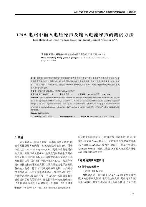
LNA电路中输入电压噪声及输入电流噪声的测试方法Test Method for Input Voltage Noise and Input Current Noise in LNA马锡春,王征宇,刘继光(中科芯集成电路有限公司,江苏无锡214072)Ma Xi-chun,Wang Zheng-yu,Liu Ji-guang(China Key System&Integrated Circuit Co.,Ltd.,Jiangsu Wuxi214072)摘要:随着5G无线网络不断发展,射频前端性能在射频接收器信号路径中扮演着越来越关键的角色,对于低噪声放大器(LNA)尤其如此。
LNA的关键指标包括工作频率范围、小信号带宽、噪声系数、增益、驻波等。
文中主要介绍了一种基于实装仪表(N9030B频谱仪)测试其前端LNA的输入电压噪声(VN)及输入电流噪声(IN)指标的方法。
关键词:低噪声放大器;输入电压噪声;输入电流噪声中图分类号:TN43;TN722.3文献标识码:A文章编号:1003-0107(2020)12-0025-04Abstract:With the development of5G wireless networks,RFfront-end performance plays an increasingly criticalrole in the signal path of RF receivers,especially for LNA.The key indicators of LNA include operating frequencyRange,-3dB Small Signal Bandwidth,Noise Figure,Gain,Harmonic Distortion,etc.This paper mainly introducesa method to measure the input voltage noise(VN)and input current noise(IN)of the LNA with a spectrometer(N9030B).Key words:LNA;VN;INCLC number:TN43;TN722.3Document code:A Article ID:1003-0107(2020)12-0025-040概述放大电路是一种弱点系统,具有很高的灵敏度,因而容易接受外界和内部一些无规则信号的影响[1]。
轮胎空腔共鸣噪声室内测试方法的研究

0 2 4 6 8 10 12 14 16 18 20 ះจஜ
(b)速度为100 km·h-1
RFVࣧϘN
140
140
3
120
2
120
RFVࣧϘN
100
100
80
4 80
1 3
60
60
1
40
40
2
4
20
20
0 2 4 6 8 10 12 14 16 18 20 ះจஜ
(c)速度为110 km·h-1
第9期
陈仁全等.轮胎空腔共鸣噪声室内测试方法的研究
567
轮胎空腔共鸣噪声室内测试方法的研究
陈仁全1,王 君2,孙 超3,唐 明2,周 磊1,贾春辉1,仇吉伟1,孙向阳1,张 超1
(1. 青岛轮云设计研究院有限责任公司,山东 青岛 266400;2. 青岛双星轮胎工业有限公司,山东 青岛 266400;3. 双 星集团有限责任公司,山东 青岛 266400)
从图2—4可以得出以下结论。 (1)在 速 度 为30~90 km·h-1时,4条 轮 胎 声 压 幅 值 未 出 现 异 常 突 变 现 象,可 以 认 为 该 速 度 段
٩ࣧܥϘdB A
ᣂᑁᣀᤳ˄rgmin1˅
1 000 900 800 700 600 500 400 300 0
8
16
24
215
100 200 300 400 ᮟညHz
(a)1#轮胎
65
1 000
64
900
63
800
٩ࣧܥϘdB A ᣂᑁᣀᤳ˄rgmin1˅
62
700
61
60
59
58 500
可控震源相关数据谐波干扰联合压制方法
可控震源相关数据谐波干扰联合压制方法曲英铭;李金丽;李振春;李国磊;黄金强【摘要】谐波是可控震源采集数据中的特殊干扰波.针对力信号内含谐波和表层响应谐波在产生机理与分布特征上的差异,提出了两种不同的相关后数据谐波干扰压制方法:①基于地面力信号设计的力信号内含谐波压制滤波器,采用最小二乘法对预测的谐波干扰进行修正,以实现对力信号内含谐波的准确压制;②分频滤波压制表层响应谐波,根据表层响应谐波的能量与频率分布特征,在不同频段对共中心点道集中的谐波进行压制.这两种谐波压制方法既可以用来直接对相关后数据的谐波噪声进行压制,也可以用来对两种谐波干扰噪声进行联合压制.实际资料试算结果表明:两种谐波干扰联合压制方法可以有效压制相关后数据中的内含谐波和表层响应谐波.%Harmonic noise is a special interference wave generated in vibroseis acquisition.Harmonic noise contained in force signal differs from surface response harmonic noise;therefore,the corresponding harmonic suppression method is proposed for the two kinds of noise in correlated data.This paper proposes a filter based on the force signal to accurately suppress the harmonic noise contained in force signal.The least squares method is then adopted to correct the predicted harmonic noise.To suppress the surface response harmonic noise,frequency division filtering is used in CMP gathers,according to the energy and frequency distribution characteristics of this kind of harmonic.The proposed method is performed on correlated data,and could realize joint suppression of two types of vibroseis harmonic noise.Data from field tests indicate that the proposed method can effectively suppress the two kinds of harmonic noise.【期刊名称】《石油物探》【年(卷),期】2018(057)002【总页数】11页(P237-247)【关键词】可控震源;力信号内含谐波;表层响应谐波;地面力信号;分频滤波【作者】曲英铭;李金丽;李振春;李国磊;黄金强【作者单位】中国石油大学地球科学与技术学院,山东青岛266580;中国石油化工股份有限公司地球物理重点实验室,江苏南京211103;中国地质科学院地球物理地球化学勘探研究所,河北廊坊065000;中国石油大学地球科学与技术学院,山东青岛266580;中国石油化工股份有限公司胜利油田分公司物探研究院,山东东营257022;中国石油大学地球科学与技术学院,山东青岛266580【正文语种】中文【中图分类】P631可控震源因其具有安全、环保、低耗、高效、方式灵活等优点而备受青睐,在全球陆上石油地震勘探采集中占有很大的比重。
NVH相关术语定义

白噪声(white noise),整个音频频率范围内,功率密度谱均匀分布且等比例宽度的能量相等的一种噪声,换句话说,此信号在各个频段上的功率是一样的,由于白光是由各种频率(颜色)的单色光混合而成,因而此信号的这种具有平坦功率谱的性质被称作是“白色的”,此信号也因此被称作白噪声。
一般用于测试音响设备的频率响应等特性。
粉红噪声(Pink Noise),是一种频率覆盖范围很宽的声音,低频能下降到接近0Hz(不包括0Hz)高频端能上到二十几千赫,而且它在等比例带宽内的能量是相等的(误差只不过0.1dB 左右)。
比如用1/3oct带通滤波器去计算分析,我们会发现,它的每个频带的电平值都是相等的(2/3oct、1/6oct、1/12oct也是一样),这就是为什么在测试声场频率特性中要用粉红噪声作为标准信号源的原因。
也是一种随机测试信号。
这种信号随着频率每升高一个八度,信号强度就衰减3dB,由于人耳对音量的感受是对数型的,所以“粉红噪声”这种每升高一个八度、强度就衰减3dB的特性,在人耳里听起来反而感觉每个频段的音量大小都是一致的。
振动:The oscillatory (back and forth) motion of a physical object.噪声:Any component of a transducer signal which does not represent the variable intended to be measured.固有频率(振动中最重要的概念):The frequency of free vibration of a mechanical system at which a specific natural mode of the system elements assumes its maximum amplitude.强迫振动:The response vibration of a mechanical system due to a forcing function (exciting force). Typically, forced vibration has the same frequency as that of the exciting force.自由振动:Vibration response of a mechanical system following an impulse-like initial perturbation (change of position, velocity or external force). Depending on the kind of perturbation, the mechanical system responds with free vibrations at one or more of its natural frequencies.绝对振动:Vibration of an object as measured relative to an inertial (fixed) reference frame. Accelerometers and velocity transducers measure absolute vibration typically of machine housings or structures; thus they are referred to as seismic transducers or inertial transducers.简谐振动:Sinusoidal vibration with a single frequency component.赫兹:(Hz) Unit of frequency measurement in cycles per second.频率:The repetition rate of a periodic vibration per unit of time. Vibration frequency is typically expressed in units of cycles per second (Hertz) or cycles per minute (to more easily relate to shaft rotative speed frequency). In fact, since many common machine malfunctions produce vibration which has a fixed relationship to shaft rotative speed, vibration frequency is often expressed as a function of shaft rotative speed. 1X is a vibration with a frequency equal to shaft rpm, 2X vibration is at twice shaft rpm, 0.5X vibration with a frequency equal to one-half shaft rpm, etc.振幅:The magnitude of periodic dynamic motion (vibration). Amplitude is typically expressed in terms of signal level, e.g., millivolts or milliamps, or the engineering units of the measured variable, e.g., mils, micrometres (for displacement), inches per second (for velocity), etc. The amplitude of a signal can bemeasured in terms of peak to peak, zero to peak, root mean square, or average.相位角:The timing relationship, in degrees, between two vibration signals, such as a Keyphasor® pulse and a vibration signal; also, the phase difference between two signals, such as the input force signal and output response signal. The "lag" corresponds to "minus" in mathematical formulations.加速度:The time rate of change of velocity. For harmonic motion, this is often expressed as g or a. Typical units for acceleration are feet per second per second (ft/s2) pk, meters per second per second (m/s2) pk, or more commonly g pk (= acceleration of earths gravity = 386.1 in/s2 = 32.17 ft/s2 = 9.81 m/s2). Acceleration measurements are generally made with an accelerometer and are typically used to evaluate high frequency vibration of a machine casing or bearing housing due to blade passing, gear mesh, cavitation, rolling element bearing defects, etc.速度:The time rate of change of displacement. Typical units for velocity are inches/second or millimetres/second, zero to peak. Velocity measurements are used to evaluate machine housing and other structural response characteristics. Electronic integration of a velocity signal yields displacement, but not position.位移:The change in distance or position of an object relative to a reference. Machinery vibration displacement is typically a peak to peak measurement of the observed vibrational motion or position, and is usually expressed in units of mils or micrometres. Proximity probes measure displacement directly. Signal integration is required to convert a velocity signal to displacement, but does not provide the initial displacement (distance from a reference) measurement.分贝:A numerical expression of the ratio of the power or voltage levels of electrical signals.dB = 10 log P1/P2 = 20 log V1/V2.共振:The condition in which the frequency of an external force coincides with a natural frequency of the system. A resonance typically is identified by an amplitude peak, accompanied by a maximum rate of change of phase lag angle.频谱:Commonly a presentation of the amplitudes of a signal's frequency components versus their frequencies. Or the frequency content of a signal.信噪比:The number formed by dividing the magnitude of the signal by the magnitude of the noise present in the signal. A low noise signal has a high Signal-to-Noise Ratio, while a high noise signal has a low Signal-to-Noise Ratio. The noise can originate from many different sources and is considered to be any part of the signal which does not represent the parameter being measured.比例阻尼:proportional damping传递矩阵法:transfer matrix method颤振:flutter 喘振:surge功率谱密度函数:power spectral density function功率谱密度矩阵:power spectral density matrix互谱密度函数:cross-spectral density function互谱密度函数:cross-spectral density matrix互相关函数:cross-correlation function混沌振动:chaotic vibration简正模态函数:normal modal function简正模态矩阵:normal modal matrix模态截断法:mode truncation method模态综合法:component modal synthesis method均值Mean value方差Variance机械阻抗Mechanical impedance位移阻抗Displacement impedance速度阻抗Speed impedance加速度阻抗Acceleration impedance声学基础知识扫盲帖(原创)1、人耳能听到的频率范围是20—20KHZ2、把声能转换成电能的设备是传声器3、把电能转换成声能的设备是扬声器4、声频系统出现声反馈啸叫,通常调节均衡器5、房间混响时间过长,会出现声音混浊6、房间混响时间过短,会出现声音发干1477、唱歌感觉声音太干,当调节混响器8、讲话时出现声音混浊,可能原因是加了混响效果9、声音三要素是指音强、音高、音色10、音强对应的客观评价尺度是振幅11、音高对应的客观评价尺度是频率12、音色对应的客观评价尺度是频谱13、人耳感受到声剌激的响度与声振动的频率有关14、人耳对高声压级声音感觉的响度与频率的关系不大15、人耳对中频段的声音最为灵敏16、人耳对高频和低频段的声音感觉较迟钝17、人耳对低声压级声音感觉的响度与频率的关系很大18、等响曲线中每条曲线显示不同频率的声压级不相同,但人耳感觉的响度相同19、等响曲线中,每条曲线上标注的数字是表示响度级20、用分贝表示放大器的电压增益公式是20lg(输出电压/输入电压)21、响度级的单位为phon22、声级计测出的dB值,表示计权声压级23、音色是由所发声音的波形所确定的24、声音信号由稳态下降60dB所需的时间,称为混响时间25、乐音的基本要素是指旋律、节奏、和声26、声波的最大瞬时值称为振幅27、一秒内振动的次数称为频率28、如某一声音与已选定的1KHz纯音听起来同样响,这个1KHz纯音的声压级值就定义为待测声音的响度29、人耳对1~3KHZ的声音最为灵敏30、人耳对100Hz以下,8K以上的声音感觉较迟钝31、舞台两侧的早期反射声对原发声起加重和加厚作用,属有益反射声作用32、观众席后侧的反射声对原发声起回声作用,属有害反射作用33、声音在空气中传播速度约为340m/s34、要使体育场距离主音箱约34m的观众听不出两个声音,应当对观众附近的补声音箱加0.1s延时35、反射系数小的材料称为吸声材料36、透射系数小的材料称为隔声材料37、透射系数大的材料,称为透声材料38、全吸声材料是指吸声系数α=139、全反射材料是指吸声系数α=040、岩棉、玻璃棉等材料主要吸收高频和中频41、聚氨酯吸声泡沫塑料主要吸收高频和中频42、薄板加空腔主要吸收低频43、薄板直接钉于墙上吸声效果很差44、挂帘织物主要吸收高、中频45、粗糙的水泥墙面吸声效果很差46、人耳通过声源信号的强度差和时间差,可以判断出声源的空间方位,称为双耳效应47、两个声音,一先一后相差5ms--50ms到达人耳,人耳感到声音是来自先到达声源的方位,称为哈斯效应48、左右两个声源,声强级差大于15dB,听声者感到声源是在声强级大的声源方位,称为德波埃效应49、一个声音的听音阈因为其它声音的存在而必须提高,这种现象称为掩敝效应50、厅堂内某些位置由于声干涉,使某些频率相互抵消,声压级降低很多,称为死点51、声音遇到凹的反射面,造成某一区域的声压级远大于其它区域称为声聚焦52、声音在室内两面平行墙之间来回反射产生多个同样的声音,称为颤动回声。
处理有色观测噪声的粒子滤波算法_范澎湃
文章编号:1673-6338(2009)02-0089-04处理有色观测噪声的粒子滤波算法范澎湃,隋立芬,黄贤源(信息工程大学测绘学院,河南郑州 450052)摘要:针对经典K alman 滤波无法直接处理有色噪声的问题,采用多项式长除法将有色观测噪声模型展开成无穷级数,截断取其有限项获得有色噪声的先验信息;然后利用粒子滤波能够处理非高斯噪声的特点对有色观测噪声进行处理。
通过一个GP S 定位算例,将此新方法与观测扩增方法进行了分析和比较。
结果证明,利用该方法能有效地控制有色观测噪声的影响。
关 键 词:K alman 滤波;有色噪声;观测扩增法;粒子滤波中图分类号:P207 文献标识码:A D OI 编码:10.3969/j.issn.1673-6338.2009.02.004Particle Filter for Colored Measurement NoiseFAN Peng -pai,SU I L-i fen,H U ANG Xian -y uan(I nstitute of Sur vey ing and M ap p ing ,I nf ormation Engineer ing Univer sity ,Zhengz hou 450052,China )Abstract:Po ly no mia-l quo tient has been used,a iming at so lv ing pro blem of the color ed measurement no ises,w hich translates colored observat ion noises into infinit e series,and the v ariances of co lo red observation noises hav e been calculat ed.P article filt er was follo wed to est imate the parameter s.In o rder to v erify the v alidity and ratio nality of this method,a contr ast bet ween this met ho d and t he appr oach of observ at ion ex pand filter w as g iv en.T he result sho wed that the the influences of the color ed o bser vatio n noises effectiv ely could be co nt rolled in t his a ppro ach.Key words:K alman filter ;color ed observ ation noises;o bserv atio n ex pand;particle filter以Kalman 滤波为代表的传统滤波方法一般是针对系统的过程噪声和观测噪声均为已知白噪声序列且方差已知的情况。
奇异值分解用于可调谐二极管激光吸收光谱技术去除系统噪声
奇异值分解用于可调谐二极管激光吸收光谱技术去除系统噪声王喆;汪曣;张锐;赵学玒;刘乔俊;李丛蓉【摘要】Detection of gas concentration with tunable diode laser absorption spectroscopy (TDLAS)techniques is affected by baseline drift and high-frequency noise.Therefore,how to remove the systematic noises has been a hot spot.This paper analyzes the significance of singular value decomposition (SVD)in TDLAS detection system with two different methods of constructing a matrix,and it discusses the differences of processing results for different noises.The second harmonic signal is arranged in a ma-trix and decomposed.We select the appropriate threshold and putthose singular values smaller than the threshold into zero,then reconstruct the matrix.Experiments show that SVD method does not require additional system components or pass into the zero gas to subtract background.This method is able to remove noises of TDLAS system quickly and effectively.We found that the method of constructing a hankel matrix is suitable for removing high-frequency noise.However,the method of constructing a continuous-cutoff-signal matrix is suitable for removing baseline drift.For example,we set up a TDLAS system to measure the concentration of NH3 while the noise removal rate of the second harmonic curve is up to 80% with this method.%可调谐二极管激光吸收光谱(TDLAS)技术用于气体浓度检测时,会受到谐波检测中基线漂移及噪声的影响,因此如何去除系统噪声一直是研究的热点。
改进的超低频广义旁瓣噪声抵消算法
改进的超低频广义旁瓣噪声抵消算法李春腾;蒋宇中;张宁;刘芳君【摘要】为了有效地改善超低频频段的通信质量,在广义旁瓣抵消算法的基础上,提出了一种改进的广义旁瓣噪声抵消算法.首先,该算法将主通道中的延时求和用线性滤波算法代替,有利于进一步提高非相干噪声的抑制能力;其次,鉴于各通道信号强度存在差异,采用优化后的阻塞矩阵代替原来的简单相减阻塞矩阵,有利于减少期望信号的残留,从而提高算法的性能;最后,采用线性滤波代替原来的自适应算法,可以在实现噪声抵消的同时不降低主天线的灵敏度,且提高算法的运算速度.为了验证所提算法的有效性,在实验室环境下搭建了实验平台,设计了多组对照实验.实验结果表明,这种模拟电路可有效地抑制工频及其谐波干扰.改进后的广义旁瓣抵消算法相比于原算法,在信噪比和噪声底限的改善上有较大的成效.%In order to improve the communication quality in extremely-low-frequency(ELF)communication, based on the generalized sidelobe cancellation(GSC)method,an improved GSC method is proposed and constructed.First,the delay summation in the main channel is replaced by the linear filtering algorithm, which is beneficial to further improving the suppression ability of incoherent noise.Second,by considering the difference in signal energy among channels,using the optimized blocking matrix can reduce the amplitude of the desired signal and improve the performance,comparing to the original blocking matrix obtained by simple subtraction among the main channels.Finally,the method using linear filtering instead of the original adaptive algorithm can achieve noise cancellation without reducing the sensitivity of the main antenna and improve the algorithm's operatingspeed.In order to verify the effectiveness of the proposed algorithm,an experimental platform is set up in laboratory environment and a series of control experiments are designed.Experimental results show that the designed analog circuits can suppress 50 Hz and its harmonic components and that the improved GSC algorithm is better than the original algorithm in terms of improvement of the signal-to-noise ratio(SNR)and the noise floor.【期刊名称】《西安电子科技大学学报(自然科学版)》【年(卷),期】2019(046)001【总页数】8页(P98-105)【关键词】超低频通信;噪声抵消;模拟电路;磁传感器;广义旁瓣抵消;线性滤波【作者】李春腾;蒋宇中;张宁;刘芳君【作者单位】海军工程大学电子工程学院,湖北武汉 430033;海军工程大学电子工程学院,湖北武汉 430033;海军工程大学电子工程学院,湖北武汉 430033;云南民族大学数学与计算机科学学院,云南昆明 650500【正文语种】中文【中图分类】TN911.7超低频频段的电磁波具有在海水中衰减较小、信号传输稳定以及抗干扰能力强等优点[1],因此,被视作一种可靠的战略通信方式。
- 1、下载文档前请自行甄别文档内容的完整性,平台不提供额外的编辑、内容补充、找答案等附加服务。
- 2、"仅部分预览"的文档,不可在线预览部分如存在完整性等问题,可反馈申请退款(可完整预览的文档不适用该条件!)。
- 3、如文档侵犯您的权益,请联系客服反馈,我们会尽快为您处理(人工客服工作时间:9:00-18:30)。
Method of reducing harmonic noise in vibroseis operations DescriptionThe invention relates to vibroseis operations and, more specifically, to the processing and analysis of signals transmitted through subsurfaces, either directly, or after various reflections on various substrata of such a subsurface.It is frequently sought to eliminate distortions or correlation noise of such signals, which appear at the stage where logged signals are finally processed.These phenomena mainly result from the undesirable appearance of harmonics of the emitted signal, harmonics which it is therefore desired to eliminate on receiving the signals.Typically, the signal is emitted by several vibrators and is in the form of a frequency sweep. The sweep is typically repetitive and often linear.A linear and repetitive signal is thus known as a "slip-sweep" signal.A slip-sweep seismic acquisition method described by H. J. Rozemond during the 66th SEG meeting in 1996, (Slip-Sweep acquisition) provided for the separation of vibroseis signals emitted by various sources and overlapping in terms of time.The seperation envisaged is only perfect if one of the two following conditions is met:the signal has no distortion;the time difference between two successive emissions is long enough that the correlation noise associated with a source does not interfere with the signal associated with the other sources.In practice, no distortion-free vibroseis source is known, and, furthermore, the need to optimize the productivity of the seismic acquisition leads to searching for time differences between vibrations which are as short as possible.Under these conditions, the recordings obtained have a signal-to-noiseratio which is worse than that which would be obtained by using sources without a time overlap.Patent GB 2 348 003 describes a method to reduce the correlation noise. This method is applicable to sets of seismograms which beforehand have been processed and grouped into mirror points (such that the reflections from the same point in space are at the same point in time or in depth). These seismograms are then decomposed into narrow frequency bands in which statistical discrimination of the signal and of the noise is carried out.Other methods have been proposed to improve vibroseis productivity.For example, it has been proposed to encode the phase of signals emitted simultaneously by n groups of vibrators.It has been shown that if n successive recordings are carried out with suitably adjusted phases, it is possible to separate the signals emitted by the n groups of vibrators. However, the separation is complete only for the fundamental part of the signal and not for its harmonics.Another possibility is to emit simultaneously in separate frequency bands. The signals generated by the various sources are mutually orthogonal and consequently may be separated from each other. However, the orthogonality is only completely applicable to the fundamentals, the presence of harmonics resulting in excess noise.Reduction in the correlation noise is therefore one of the keys to increasing vibroseis productivity, and the techniques proposed to date have been shown to be unsatisfactory.The main aim of the present invention is a method of improved efficiency for eliminating harmonics in a vibroseis signal.The aim of the present invention is thus especially to make it possible to reduce the correlation noise in individual seismograms, for example before any processing, by using the time/frequency transform to separate the signal from the correlation noise.These aims are achieved according to the invention using a vibroseis analysis method in which frequency-sweep signals are emitted into a subsurface, the signals reflected on the substrata of such a subsurface are logged and the logged signals are processed, a method in which the harmonics of the fundamental signal initially emitted are eliminated from the logged signals, by applying the steps consisting in:a) providing a time/frequency plot, showing the respective contributions of the fundamental and of the harmonics in the logged signal,b) providing a time/frequency plot also showing these contributions of the fundamental and of the harmonics in the logged signal, this plot having been stretched in the direction of the frequency axis such that the fundamental of this plot is over the location of a harmonic chosen from the plot;c) adapting the power amplitude of this stretched plot to make this amplitude correspond to that of the said chosen harmonic of the plot;d) subtracting these two plots one from the other such that the said chosen harmonic is eliminated, by subtraction with the fundamental of the stretched plot.Other characteristics, aims and advantages of the invention will become apparent on reading the following detailed description, made with reference to the appended figures in which:FIG. 1 is a time/frequency plot showing a slip-sweep signal;FIG. 2 illustrates the preparation of a time/frequency plot by means of a series of graphs corresponding to various sweep rates, in this case those of the fundamental and of some harmonics;FIG. 3 shows a trace of a time/frequency plot including the contribution of the fundamental and the contributions of various harmonics;FIG. 4 is a time/frequency plot showing a given sweep of the same slip-sweep signal, without any particular processing;FIG. 5 is a time/frequency plot showing a given sweep of the same slip-sweep signal, after filtering accentuating the contribution of the fundamental;FIG. 6 shows a time/frequency plot showing a given sweep of the same slip-sweep signal, after filtering accentuating the contribution of a chosen n th harmonic;FIG. 7 is a time/frequency plot showing a given sweep of the same slip-sweep signal obtained after accentuating the fundamental and stretching along the frequency axis;FIG. 8 is a time/frequency plot showing a given sweep of the same slip-sweep signal, obtained from the plot of FIG. 7 by applying a matching operator;FIG. 9 is a time/frequency plot obtained after a subtraction intended to eliminate the n th harmonic.A favoured implementational example of the invention will now be described, in this case applied to the processing of signals of the slip-sweep type.However, the invention is applicable for processing many signals used in vibroseis operations, and especially to other types of linear or non-linear, repetitive or non-repetitive frequency sweeps.FIG. 1 shows a time/frequency plot corresponding to the signal logged at the surface after passing through and possible reflection in a subsurface.In this plot, the segments 10 with a small gradient, shown in bold line, correspond to the fundamental frequency-sweep rate, that is to say the sweep rate of vibrators placed on the surface of the ground.A series of fine lines whose gradients are each equal to a multiple of the gradient of the fundamental, correspond, simultaneously, to each fundamental sweep 10 in FIG. 1.These other segments 20, of steeper gradient, correspond to the unwanted harmonics which appear on top of the fundamental sweep.In the case of the slip-sweep (linear repetitive sweep), the fundamental 10 of the signal is shown in the time/frequency plane by the straight line of equation:(f-fs )/fe-fs)=t/tswhere fs is the starting frequency of the sweep emitted, feis the finalfrequency of the sweep emitted, and tsis the time at which the sweep starts. The n th harmonic is itself given by the straight line:(f-nfs )/n(fe-fs)=t/tsA reflection at time twill be represented by the set of straight lines of equation:(f-nfs )/n(fe-Fs)=(t-t)/tsEach of these lines 10, 20 will correspond respectively to the fundamental (for n=1) and to its harmonics (for n>1), these straight lines having the same gradient as the fundamental and the harmonics of the signal.In the T, F plot of FIG. 1, for a given time t on the time axis, a point 11 of the fundamental 10, at a frequency f, gives rise to points 12, 13,14 of the harmonic 20 at multiple frequencies 2f0, 3f, . . . , nf0.The appearance of a particular power at a given time and frequency is manifested by a power undulation. Thus, a section of the T, F plot at a given time t on the time axis provides a graph like that of FIG. 3.The point 11 of the fundamental consisting of a fluctuation of power at the frequency f, and the points 12, 13, . . . corresponding to the energiesof the harmonics, consisting of power fluctuations at the frequencies 2f,3f0, . . . nf. . . will be found therein.The amplitude fluctuations of the harmonics are therefore placed at frequencies proportional to the order of the harmonic in question.In this figure, the power fluctuations corresponding to the harmonics(frequencies 2f0, 3f, . . . , nf. . . ) appear to be wider the higherthe order of the harmonic in question.More specifically, it turns out that the fluctuations have widths which are substantially proportional to the order of the harmonic in question.This broadening, which is proportional to the frequency of the harmonic, can be explained as follows.It may be recalled that the frequency transform, by means of which the time/frequency plot is plotted, is obtained by Fourier transformation of the signal logged over successive time windows, each one of short duration.Each point of the time/frequency plot consists in carrying out the Fourier transform of the product of the logged signal, a time window and a "tapper" (apodization function).Since the logged signal consists of the sum of a fundamental h1and ofseveral harmonics h2, h3, h4, its Fourier transform is, in other words,the sum of transforms of sweeps or different frequencies (H1, H1, . . . ,Hn, . . . ), sweeps which are different but however limited over the same time window (FIG. 2).Thus, in the case of a vibroseis signal with distortion, the Fourier transform for any time window may be written:FEN(F)=TAP*[H1 H2. . . Hn]Limiting the fundamental sweep to a given time window limits it to a narrow frequency range, while this same time window allows the harmonics to cover a wider frequency range.As shown in FIG. 2, in the frequency domain, the frequency ranges covered by the sweeps are shown by the pulses 31, 32, 33, . . . , and these pulses, described in the given time window, are broader the higher the order of the harmonics.After application of a tapper 40, the fluctuations 51, 52, 53, . . . , are obtained, which are themselves of a width proportional to the order of the harmonic.In order to eliminate the power of the harmonics from the time/frequency (T-F) plot, it is proposed to make use of such a pseudo-periodicity in frequencies of the fluctuations (and therefore of the contributions) of the fundamental and of the harmonics, and even in this case preferably to take out part of the spread, the width of which is proportional to the order of the harmonics.To do this, a multiplicative factor is applied to the T-F plot along the frequency axis, the effect of this operation being to stretch the plot along the frequency axis.The multiplying factor is chosen to be equal to the order of one harmonic 20 to be removed, such that the fundamental 10 of the stretched plot is in the position of the harmonic to be eliminated.Then, a subtraction between the initial T-F plot and the plot stretched in this way is carried out.Before the subtraction, a matching operator is applied to one or other of these plots, for the purpose of making the power amplitudes of the stretched fundamental correspond with the harmonic to be eliminated.Thus, before the subtraction, the fundamental 10 is in the position ofthe harmonic 20 to be eliminated by virtue of the stretching, with the same power amplitude due to applying the matching operator.A subtraction of this sort, after bringing the frequencies and amplitude into line, turns out to be particularly effective for eliminating the harmonic in question.As mentioned above, a plot of this sort having undergone this subtraction by the stretched plot is ideally processed again in order to remove other harmonics still present.The aforementioned steps are implemented again, in order to eliminate each unwanted harmonic, until the fundamental appears markedly more distinct than the remaining harmonics.These various steps will now be described in more detail.In the method described here, a matching operator is first of all determined specifically before each subtraction in question, by means of a preliminary phase of optimizing this operator which will now be described.Here, the determination of this operator is based on optimizing a preliminary subtraction between two plots, one stretched and matched, the other unstretched.The two plots used in this phase for determining the operator are plots which have undergone filtering to accentuate the contributions having to cancel each other out.Thus, in this optimization phase, a respective filter is applied to each plot used, which accentuates the contributions of the fundamental on the one hand and the harmonic to be eliminated on the other.FIG. 5 thus shows a stretched plot in which the contribution of the fundamental has been accentuated by filtering.FIG. 6 shows an unstretched plot, in which the contribution of the n th harmonic, to be eliminated, is accentuated.Since the frequency pseudo-periodicity, described above, is a property independent of the window for calculating the Fourier transform, the accentuating filtering is particularly easy.A filter accentuating the frequencies close to those of the fundamental, applied in the same way at each time in question for the time/frequency plot, gives satisfactory results. Constant filtering over the whole time/frequency plane even provides satisfactory results although being very simple.A matching operator is applied, in this case by convolution, to the filtered and stretched plot of FIG. 5, then this plot is subtracted from the unstretched plot of FIG. 6, in which the n th harmonic has been accentuated by filtering.The operator may be a simple multiplicative scalar factor, or a more complex operator, incorporating several variables to be optimized.Finally, the choice of operator is optimized so that the subtraction of these two accentuated plots comprises, at the location of the n th harmonic, a minimum manifestation of the latter.The matching operator is then used to optimum benefit in a following subtraction phase for effective elimination of the n th harmonic.More specifically, the n th harmonic is in this case eliminated from a plot with no accentuating filtering, as shown in FIG. 4.As a result, any deformation of the fundamental introduced by filtering is avoided in the plot. In contrast, in this case, it is chosen to apply the matching operator not to a stretched raw plot, but to the stretched and filtered raw plot mentioned above, that is to say to the stretched plot having undergone filtering accentuating the fundamental. The matching operator is in this case applied by convolution.This is because, the fundamental 10, although slightly deformed by filtering, is only a slight problem when this fundamental is subtracted from a harmonic.A stretched plot, in which the fundamental 10 has been accentuated beforehand (FIG. 7 and FIG. 8) is therefore subtracted from the plot of FIG. 4.Furthermore, with regard to the stretched plot, such accentuating filtering makes it possible to reduce the contributions of the harmonics offset to higher orders, which prevents any undesired manifestation in the high orders after subtraction.As shown in FIG. 9, the plot obtained after subtraction has an unchanged fundamental 10 and an almost removed nth order harmonic, reference 20. By virtue of this operation, the other harmonics are also strongly reduced since they are subtracted by offset harmonics.For subsequent elimination operations, the plot of this same FIG. 9, that is to say the resulting plot obtained from this iteration, will be used.In the present example, advantage is taken not only of the periodicity of the power undulations (contributions), but also of the fact that the harmonics have widths which are multiples of the width of the fundamental.In other words, by stretching the fundamental by a ratio equal to the orderof the contribution of the harmonic to be eliminated, not only the centre fof the 10 of the fundamental is placed in the position of the centre nf0 contribution of the n th harmonic, but the width of the contribution of the fundamental is also stretched, which has the effect of making the width correspond suitably with the contribution of the harmonic in question.A second advantage of this subtraction by a stretched plot resides in the fact that the fundamental is found to be the sweep having the smallest gradient.Thus, in the stretched plot of FIG. 7, there is no segment below the fundamental stretched segment 10, therefore no segment is superimposed in the plot, below the n th harmonic which it is desired to eliminate. Thus, by carrying out harmonic eliminations in a successive and increasing order, the eliminations of the previous harmonics are not damaged.In addition, the harmonics 20 of the stretched plot are placed so as to overlap other harmonics of the initial plot, such that by subtraction they have an effect of decreasing the manifestations of these other harmonics. Of course, there are other variant embodiments of the invention. For example, it is possible to apply a matching operator to a stretched plot, without accentuation, then to subtract this stretched plot from the plot for elimination of the harmonic.The matching operator may, in the same way, be determined from plots having undergone accentuation filtering, or from unfiltered plots.。