BF1206,115;中文规格书,Datasheet资料
1206封装芯片LED(1.0毫米高度)说明书

Prepared date: 12-Aug.-2009
Rev 1
Page: 3 of 10
Prepared by: Changhong Pan
Bin Range Of Dom. Wavelength
Group
Bin
Min.
Max.
W
515
520
X
X
1000 Hrs. 22 PCS. 0/1
5
Low Temperature Storage
Temp. : -40℃
1000 Hrs. 22 PCS. 0/1
6 DC Operating Life
IF = 20 mA
1000 Hrs. 22 PCS. 0/1
7
High Temperature / High Humidity
telephone and fax. ․Flat backlight for LCD, switch and symbol. ․General use.
Device Selection Guide
PART No. 15-21/GHC-XS1T1/2T
Chip Material
InGaN
Emitted Color Brilliant Green
λd
515
-----
Spectrum Radiation Bandwidth
△λ
-----
35
Forward Voltage
VF
2.7
3.3
Reverse Current
IR
-----
-----
Max. 360 --------530 -----
3.7 50
Unit Condition
贴片LED1206规格书

SEC.A-A
A
1.75 [0.07"]
0.20 [0.01"]
5.25 [0.21"]
8.00 [0.31"]
1.05 [0.04"] 4.00 [0.16"]
A
�
Arrangement of Tape
500 hrs
0/22
Low Temperature Life Test
1000 hrs
0/22
TAIWAN TONGJIA OPTOELECTRONICS TECHNOLOGY CO., LTD DONGGUAN TONGJIA OPTOELECTRONICS TECHNOLOGY CO., LTD
Test circuit and handling precautions
� Test circuit
+ -
R V
LED
� Handling precautions 1. Over-current-proof Customer must apply resistors for protection; otherwise slight voltage shift will cause big current change (Burn out will happen). 2. Storage 2.1 It is recommended to store the products in the following conditions: Humidity: 60% R.H. Max. Temperature : 5℃~30℃(41℉~86℉) 2.2 Shelf life in sealed bag: 12 month at <5℃~30℃ and <30% R.H. after the package is Opened, the products should be used within a week or they should be keeping to stored at≦20 R.H. with zip-lock sealed. 3. Baking It is recommended to baking before soldering when the pack is unsealed after 72hrs. The Conditions are as followings: 3.1 60±3℃ x(12~24hrs) and <5%RH, taped reel type 3.2 100±3℃ x(45min~1hr), bulk type 3.3 130±3℃ x(15~30min), bulk type
VFCP1206中文资料

Document Number: 63106For any questions, contact: foil@VFCP Series (0805, 1206, 1506, 2010, 2512) (Z-Foil)Vishay Foil ResistorsUltra High Precision Z-Foil Flip Chip Resistor with TCRof ± 0.05 ppm/°C, 35 % Space Saving versusWraparound Design and PCR of 5 ppm at Rated PowerI MP R O V E D P R O D UC Any value at tolerance available within resistance rangeINTRODUCTIONOne of the most important parameters influencing stability is the Temperature Coefficient of Resistance (TCR). Although the TCR of Bulk Metal ® Foil resistors is considered extremely low, this characteristic has been further refined over the years.The VFCP Series utilizes ultra precision Bulk Metal ® Z-Foil.The Z-Foil technology provides a significant reduction to the resistive element’s sensitivity to ambient temperaturevariations (TCR) and to self heating when power is applied (power coefficient).Along with the inherently low PCR and TCR, Z-Foil technology also provides remarkably improved load life stablility, low noise and availability of tight tolerance.The Flip Chip configuration provides a substantial PCB space saving of more than 35 % vs. a surface mount chip with wraparound terminations. The VFCP is available in any value within the specified resistance range.Our Application Engineering Department is available to advise and make recommendations. For non-standard technical requirements and special applications, please contact us.FEATURES•Temperature Coefficient of Resistance (TCR):± 0.05 ppm/°C typical (0 °C to + 60 °C)± 0.2 ppm/°C typical (- 55 °C to + 125 °C, +25 °C Ref.)•Tolerance: to ± 0.01 % (100 ppm) •Power Coefficient “ΔR due to self heating”5 ppm at Rated Power•Load Life Stability (70 °C for 2000 hours): ± 0.005 % (50 ppm)•Power Rating to: 600 mW at + 70 °C•Electrostatic Discharge (ESD) above 25 000 V•Resistance Range: 10Ω to 150 k Ω (for lower and higher values, please contact us)•Non Inductive, Non Capacitive Design •Short time overload ≤ 0.005 % (50 ppm)•Non hot spot design•Rise time: 1ns without ringing •Current Noise: - 40 dB•Voltage Coefficient < 0.1 ppm/V •Non Inductive: < 0.08 µH•Terminal Finishes available:Lead (Pb)-freeTin/Lead Alloy•Matched sets are available per request•Any value available within resistance range (e.g. 1K2345)•Prototype samples available from 48 hours. For more information, please contact foil@ •For better performances please contact usAPPLICATIONS•Automatic Test Equipment (ATE)•High Precision Instrumentation •Laboratory, Industrial and Medical •Audio•EB Applications (electron beam scanning and recording equipment, electron microscopes)•Military and Space •Airborne•Down Hole instrumentation •Communication* Pb containing terminations are not RoHS compliant, exemptions may apply TABLE 1 - TOLERANCE AND TCR VSRESISTANCE VALUERESISTANCEVALUE(Ω)TOLERANCE(%)TYPICAL TCR AND MAX. SPREAD (- 55 °C to + 125 °C,+ 25 °C Ref.)250 to 150K± 0.01± 0.2 ± 1.6100 to < 250± 0.02± 0.2 ± 1.650 to < 100± 0.05± 0.2 ± 1.825 to < 50± 0.1± 0.2 ± 2.810 to < 25± 0.25± 0.2 ± 2.8Bottom ViewRoHS*COMPLIANTVFCP Series (0805, 1206, 1506, 2010, 2512) (Z-Foil)Vishay Foil Resistors Ultra High Precision Z-Foil Flip Chip Resistor with TCRof ± 0.05 ppm/°C, 35 % Space Saving versusWraparound Design and PCR of 5 ppm at Rated Power For any questions, contact: foil@Document Number: 63106I M P R O V E D P R Note• For VFCP0805, VFCP1506, VFCP2010 and VFCP2512 DSCC Drawings, please contact foil@Note1.As shown + 0.01 W to allow for measurement errors at low values.TABLE 2 -DSCC SPECIFICATIONS (Vishay resistors are listed on the following DSCC specifications)MODEL DSCC MIL SPEC VFCP12062009MIL-PRF-55342TABLE 3 - SPECIFICATIONSCHIP SIZE RATED POWER (mW)at + 70 °C MAXIMUM VOLTAGE RATING (≤)RESISTANCERANGE (Ω)MAXIMUMWEIGHT(mg)0805100 mW34 V10 to 12K5.21206250 mW 86 V 10 to 30K 10.31506300 mW 109 V 10 to 40K122010400 mW200 V10 to 100K 252512600 mW 220 V10 to 150K35P R ×TABLE 4 - LOAD LIFE STABILITY(+ 70 °C FOR 2000 HOURS)CHIP SIZE MAXIMUM ΔR LIMITS0805± 0.005 % at 50 mW ± 0.01 % at 100 mW1206± 0.005 % at 150 mW ± 0.01 % at 250 mW 1506± 0.005 % at 150 mW ± 0.01 % at 300 mW 2010± 0.005 % at 200mW ± 0.01 % at 400 mW2512± 0.005 % at 500 mW ± 0.01 % at 600 mWTABLE 5 - PERFORMANCESTEST OR CONDITIONMIL-PRF-55342CHARACTERISTIC EΔR LIMITSTYPICAL ΔR LIMITS MAXIMUM ΔR LIMITS 1)Thermal Shock ± 0.1 %± 0.005 % (50 ppm)± 0.01 % (100 ppm)Low T emperature Operation ± 0.1 %± 0.005 % (50 ppm)± 0.01 % (100 ppm)Short Time Overload± 0.1 %± 0.005 % (50 ppm)± 0.01 % (100 ppm)High Temperature Exposure ± 0.1 %± 0.01 % (100 ppm)± 0.02 % (200 ppm)Resistance to Soldering Heat ± 0.2 %± 0.005 % (50 ppm)± 0.015 % (150 ppm)Moisture Resistance± 0.2 %± 0.005 % (50 ppm)± 0.02 % (200 ppm)Load Life Stability + 70 °C for 2000 hours at Rated Power± 0.5 %± 0.005 % (50 ppm)± 0.01 % (100 ppm)Document Number: 63106For any questions, contact: foil@VFCP Series (0805, 1206, 1506, 2010, 2512) (Z-Foil)Ultra High Precision Z-Foil Flip Chip Resistor with TCR of ± 0.05 ppm/°C, 35 % Space Saving versusWraparound Design and PCR of 5 ppm at Rated PowerVishay Foil ResistorsI Mnd Pattern Dimensions are per IPC-782Note•The TCR values for < 100Ω are influenced by the termination composition and result in deviation from this curveVFCP Series (0805, 1206, 1506, 2010, 2512) (Z-Foil)Vishay Foil Resistors Ultra High Precision Z-Foil Flip Chip Resistor with TCRof ± 0.05 ppm/°C, 35 % Space Saving versusWraparound Design and PCR of 5 ppm at Rated Power For any questions, contact: foil@Document Number: 63106I M P R O V E D P R O D U C TNote* For non-standard requests, please contact Application Engineering.TABLE 7 - GLOBAL PART NUMBER INFORMATIONNEW GLOBAL PART NUMBER:Y162910K0000T9W (preferred part number format)DENOTES PRECISIONVALUE AER*YR = ΩK = k Ω0 = Standard9 = Lead (Pb)-free 1 - 999 = CustomPRODUCT CODERESISTANCE TOLERANCEPACKAGING1629 = VFCP08051630 = VFCP12061631 = VFCP15061632 = VFCP20101633 = VFCP2512T = ± 0.01 %Q = ± 0.02 %A = ± 0.05 %B = ± 0.10 %C = ± 0.25 %D = ± 0.50 %F = ± 1.00 %R = Tape and Reel W = Waffle PackFOR EXAMPLE: ABOVE GLOBAL ORDER Y1629 10K0000 T 9 W:TYPE: VFCP0805VALUE: 10.0 k ΩABSOLUTE TOLERANCE: ± 0.01 %TERMINATION: Lead (Pb)-free PACKAGING: Waffle PackHISTORICAL PART NUMBER:VFCP080510K000TCR0.2T S W (will continue to be used)VFCP080510K000TCR0.2TSWMODELOHMIC VALUETCRRESISTANCE TOLERANCE TERMINATIONPACKAGINGVFCP0805VFCP1206VFCP1506VFCP2010VFCP251210.0 k ΩCharacteristicT = ± 0.01 %Q = ± 0.02 %A = ± 0.05 %B = ± 0.10 %C = ± 0.25 %D = ± 0.50 %F = ± 1.00 %S = Lead (Pb)-free B = Tin/LeadT = Tape and Reel W = Waffle Pack6291KY1T9WDisclaimer Legal Disclaimer NoticeVishayAll product specifications and data are subject to change without notice.Vishay Intertechnology, Inc., its affiliates, agents, and employees, and all persons acting on its or their behalf (collectively, “Vishay”), disclaim any and all liability for any errors, inaccuracies or incompleteness contained herein or in any other disclosure relating to any product.Vishay disclaims any and all liability arising out of the use or application of any product described herein or of any information provided herein to the maximum extent permitted by law. The product specifications do not expand or otherwise modify Vishay’s terms and conditions of purchase, including but not limited to the warranty expressed therein, which apply to these products.No license, express or implied, by estoppel or otherwise, to any intellectual property rights is granted by this document or by any conduct of Vishay.The products shown herein are not designed for use in medical, life-saving, or life-sustaining applications unless otherwise expressly indicated. Customers using or selling Vishay products not expressly indicated for use in such applications do so entirely at their own risk and agree to fully indemnify Vishay for any damages arising or resulting from such use or sale. Please contact authorized Vishay personnel to obtain written terms and conditions regarding products designed for such applications.Product names and markings noted herein may be trademarks of their respective owners.元器件交易网Document Number: 。
slf系列贴片电感datasheet
特点 ●是最适用于电源系统的低直流电阻,大电流,节能型产品。 ●因采用磁力屏蔽结构,所以可实现高密度安装。 ●底面为平直的低背型 , 可稳定地安装在电路板上。 ●采用卷带仕样,支持自动插入机。 用途 手机,计算机,硬盘驱动器,其他各种电子设备 仕样
工作温度范围 保存温度范围 –20 to +85°C [包括自身温度上升] –40 to +85°C [产品单体]
电气特性
电感 (H) 4.7 6.8 10 15 22 33 47 68 100 150 220 电感容差 ±20% ±20% ±20% ±20% ±20% ±20% ±20% ±20% ±20% ±20% ±20% L 测定频率 (kHz) 100 100 100 100 100 100 100 100 100 100 100 直流电阻 ( )±20% 0.0284 0.0354 0.0532 0.0745 0.104 0.148 0.21 0.29 0.43 0.65 0.98 额定电流 (A) 基于电感 变化率时 1.6max. 1.5max. 1.3max. 1max. 0.77max. 0.69max. 0.59max. 0.5max. 0.42max. 0.34max. 0.26max. 基于温度 上升时 2.5typ. 2.2typ. 1.8typ. 1.4typ. 1.3typ. 1.1typ. 0.92typ. 0.78typ. 0.64typ. 0.5typ. 0.38typ. 品名 SLF6028T-4R7M1R6-PF SLF6028T-6R8M1R5-PF SLF6028T-100M1R3-PF SLF6028T-150M1R0-PF SLF6028T-220MR77-PF SLF6028T-330MR69-PF SLF6028T-470MR59-PF SLF6028T-680MR50-PF SLF6028T-101MR42-PF SLF6028T-151MR34-PF SLF6028T-221MR26-PF
FC1206A-1R00-FB中文资料
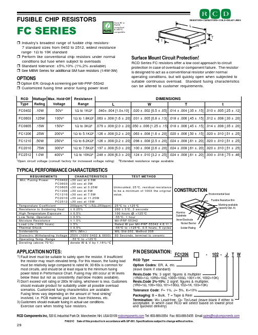
Industry’s broadest range of fusible chip resistors- 7 standard sizes from 0402 to 2512, widest resistance range- 1Ω to 10K standardPerform like conventional chip resistors under normal conditions but fuse when subject to overloads Standard tolerance: ±5%,10% (1%,2% available)See MBW Series for additional SM fuse resistors (1/4W-3W)FUSIBLE CHIP RESISTORSFC SERIESSurface Mount Circuit Protection!RCD Series FC resistors offer a low cost approach to circuit protection in case of overload or component failure. The resistor is designed to act as a conventional resistor under normaloperating conditions, but will quickly open when subjected to suitable continuous overload. Standard fusing characteristics can be altered to customer requirements.OPTIONSOption ER: Group A screening per Mil-PRF-55342 Customized fusing time and/or fusing power levelTYPICAL PERFORMANCE CHARACTERISTICSLTtW1Open circuit voltage (consult factory for increased voltage rating) 2Extended resistance range availableCONSTRUCTIONFusible Resistive filmI nner ElectrodeAlumina Substrate Nickel BarrierSolder PlatingEnvironmental Seal Marking available (specify Opt. A)Fault level must be suitable to safely open the resistor. If insufficient the resistor may reach elevated temp. For this reason, the fusing load must be relatively large compared to rated W, 30-60x is common for most circuits, and should be at least equal to the minimum fusingpower listed in Performance Chart. Fusing may still occur at W levels below these but not as consistently (fast-blow models available).Don’t exceed volt rating or 200x W rating, whichever is less. Customers should evaluate product for suitability under all possible overload scenarios. Customized fusing characteristics are available.Fusing times vary depending on the amount of “heat sinking”involved, i.e. PCB material, pad size, trace thickness, etc.Customers should evaluate fusing in actual-use conditions.Exercise care when testing fuse resistors.APPLICATION NOTES:D C R e g a t t a W M f O -d l o H .x a f R e c n a t s i s e D N O I S NE M I ST p y e g n i t a R g a t l o V e g n a R e LW T tF 2040C .01W V 0511Ωo t 1K Ω2040.±00..1[41.±00]020.±00.25.0[±.05]410.±400.53.[±51.]10.0±00.5.[52±.1]2C F 30601.52W V 00111Ωo t 8.1K Ω20.36±00.8[.16±.20]0.31±500.8.0[±]31.810.±600.54.[±]51.10.2±800.03.[±2.0]C F 5080W 51.51V 011Ωo t 3K Ω2970.±00.80.2[±.20]050.±52.1[600.±]51.810.±600.54.[±]51.410.±800.53.[±2.0]C F 6021W 52.02V 011Ωo t 1.5K Ω2621.±00.8[2.3±.20]360.±00.86.1[±.20]020.±600.05.[±]51.020.±15.[010.±]52.C F 0121W 05.25V 011Ωo t 2.6K Ω221..±60082.3[±.20]890.±800.5.2[±2.0]420.±800.16.[±2.0]020.±010.15.[±]52.102C F 0.57W 3V 0011Ωo t 5.7K Ω2800.±791.2.±0.5[0].±6.2[800.±001.]02420.±800.16.[.±20]020.±010.15.[±]52.2152C F 0.1W4V 0011Ω01o t K Ω22.48±800.3.6[±2.0]21.4±010.2.3[±]52.420.±800.16.[±2.0]030.±810.57.[±]64.ST N E M E R I U Q E R S C I T S I R E T C A R A H C D O H T E M T S E T :2040C F r e w o P g n i s u F .n i M :3060C F :5080C F :6021C F :0121C F :0102C F :2152C F W 5.2t a c e s 03<W 3t a c e s 03<W 52.3t a c e s 03<W 5t a c e s 03<W 5.7t a c e s 03<W 52.11t a c e s 03<W51t a c e s 03<e c n a t s i s e r l a u d i s e r ,C °52,d e t n u o m n U l a n i g i r o e h t X 001f o m u m i n i m a e b o t .e u l a v tn e i c i f f e o C e r u t a r e p m e T 5<(C °/m p p 002Ω)m p p 052=C °521+o t C °52t a e H g n i r e d l o S o t e c n a t s i s e R %52.0±s d n o c e s 3,C °5±062e r u s o p x E e r u t a r e p m e T h g i H %5.0±C °521+@s r u o h 001n o i t a r e p O .p m e T w o L %5.0±r u o h 1,C °55-e c n a t s i s e R e r u t s i o M %5.1±24355-F R P -l i M )s r u o h 0001(e f i L d a o L %5±1.11.8.424355-F R P -l i M r e p W d e t a R k c o h S l a m r e h T %5.0±s e l c y c 5,s r u o h 5.0,C °521+o t C °55-yt i l i b a r e d l o S ).n i M (%59802d o h t e M ,202-d t S -L I M e g a t l o V g n i d n a t s h t i W c i r t c e l e i D )3060&2040V 001(V 052c i m a r e c o t l a n i m r e t ,s d n o c e S 06e g n a R .p m e T g n i t a r e p O C°521+o t C °55-)C °07e v o b a (g n i t a r eD C°/%81.1y b V &W e t a r e d Tel: 603-669-0054 Fax: 603-669-5455 Email:sales@291)2)3)Termination: W= Lead-free, Q= Tin/Lead (leave blank if either is acceptable, in which case RCD will select based on lowest price and quickest delivery)P/N DESIGNATION:FC1206 - 102 - J T WOption Codes : ER, A, etc.(leave blank if standard)RCD TypeTolerance Code : F= 1%, J= 5%, K=10%Packaging : B = Bulk, T = Tape & ReelResis.Code 1%: 3 signif. figures & multiplier(1R00=1Ω, 10R0=10Ω, 1000=100Ω, 1001=1K, 1002=10K)Resis.Code 2%-10%: 2 signif. figures & multiplier,(1R0=1Ω, 100=10Ω, 101=100Ω, 102=1K, 103=10K )Term.W is RoHS compliant & 260°C compatible元器件交易网。
贴片压敏电阻1206封装参数型号规格书大全
T2
20 uS 1000 uS
Characteristic
Test method and description
The specimen shall be subjected to 125℃ for 1000 hours in a thermostatic bath without High Temperature Storage load and then stored at room temperature and humidity for 1 to 2 hours. The change of
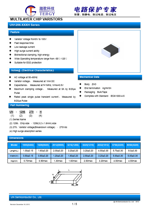
MULTILAYER CHIP VARISTORS
UN1206-XXXH Series
Feature
Varistor Voltage from5V to 100V Fast response time Low leakage current High surge current ability Bidirectional clamping, high energy Wide Operating temperature range from -55℃-125℃ Suitable for ESD protection
Dimensions
Model 1005(0402) 1608(0603) 2012(0805) 3216(1206) 3225(1210) 4532(1812) 5750(2220) 8050(3220)
Length(L) Width(W) High(H)
1.00±0.15 0.50±0.15 0.70max
Notes@(Electrical Characteristics)
AC voltage at 50~60Hz Varistor voltage: Measured at 1mA DC Capacitance: Measured at f=1MHz, Vrms=0.5V Maximum clamping voltage : Measured at 5A by 8/20µs
PMEM4020APD,115;中文规格书,Datasheet资料
1.Product profile1.1General descriptionCombination of a PNP transistor with low V CEsat and high current capability and a planar Schottky barrier rectifier with an integrated guard ring for stress protection in a SOT457(SC-74) small plastic package. NPN complement: PMEM4020AND1.2FeaturesI 600 mW total power dissipation I High current capability up to 2 AI Reduces printed-circuit board area required I Reduces pick and place costs I Small plastic SMD package ITransistorN Low collector-emitter saturation voltage I DiodeN Ultra high-speed switching N Very low forward voltage N Guard ring protected1.3ApplicationsI DC-to-DC converters I Inductive load driversI General purpose load driversI Reverse polarity protection circuits IMOSFET drivers1.4Quick reference dataPMEM4020APDPNP transistor/Schottky rectifier moduleRev. 02 — 31 August 2009Product data sheetTable 1.Quick reference data Symbol ParameterConditions Min Typ Max Unit PNP transistorV CEO collector-emitter voltage open base --−40V I Ccollector current (DC)continuous;T s ≤ 55°C[1]--−2A[1]Soldering point of collector or cathode tab.2.Pinning information3.Ordering information4.Marking5.Limiting valuesSchottky barrier rectifierV R continuous reverse voltage --40V I Fcontinuous forward current--1ATable 1.Quick reference data …continued Symbol ParameterConditionsMin Typ Max Unit Table 2.Discrete pinningPin Description Simplified outline Symbol1emitter 2not connected 3cathode 4anode 5base 6collector132456sym04036145Table 3.Ordering informationType numberPackage NameDescriptionVersion PMEM4020APDSC-74plastic surface mounted package; 6 leadsSOT457Table 4.MarkingType number Marking code PMEM4020APDD3Table 5.Limiting valuesIn accordance with the Absolute Maximum Rating System (IEC 60134).Symbol ParameterConditions Min Max Unit PNP transistorV CBO collector-base voltage open emitter -−40V V CEO collector-emitter voltage open base -−40V V EBOemitter-base voltageopen collector-−5V[1]Mounted on a FR4 printed-circuit board, single-sided copper, tin-plated, standard footprint.[2]Device mounted on a printed-circuit board, single-sided copper, tin-plated, 1cm 2 mounting pad for both collector and cathode.[3]Mounted on a ceramic printed-circuit board, single-sided copper, tin-plated, standard footprint.[4]Soldering point of collector or cathode tab.I Ccollector current (DC)continuous [1]-−0.75A continuous [2]-−1A continuous [3]-−1.3A continuous;T s ≤ 55°C[4]-−2A I CM peak collector current -−3A I BM peak base current -−1A P tottotal power dissipationT amb ≤ 25°C [1]-295mW T amb ≤ 25°C [2]-400mW T amb ≤ 25°C [3]-500mW T s ≤ 55°C[4]-1000mW T j junction temperature -150°C Schottky barrier rectifierV R continuous reverse voltage -40V I F continuous forward voltage -1A I FRM repetitive peak forward currentt p ≤ 1 ms;δ≤ 0.5- 3.5A I FSM non-repetitive peak forward currentt = 8 ms; square wave -10A P tottotal power dissipationT amb ≤ 25°C [1]-295mW T amb ≤ 25°C [2]-400mW T amb ≤ 25°C [3]-500mW T s ≤ 55°C[4]-1000mW T j junction temperature [2]-150°C Combined deviceP tot total power dissipation T amb ≤ 25°C[2]-600mW T stg storage temperature −65+150°C T ambambient temperature[2]−65+150°CTable 5.Limiting values …continuedIn accordance with the Absolute Maximum Rating System (IEC 60134).Symbol ParameterConditions Min Max Unit6.Thermal characteristics[1]For Schottky barrier rectifiers thermal run-away has to be considered, as in some applications the reverse power losses P R are a significant part of the total power losses. Nomograms for determining the reverse power losses P R and I F(AV) rating will be available on request.[2]Soldering point of collector or cathode tab.[3]Mounted on a ceramic printed-circuit board, single-sided copper, tin-plated, standard footprint.[4]Device mounted on a printed-circuit board, single-sided copper, tin-plated, 1cm 2 mounting pad for both collector and cathode tab.[5]Mounted on a FR4 printed-circuit board, single-sided copper, tin-plated, standard footprint.Table 6.Thermal characteristics [1]Symbol Parameter Conditions Min Typ Max Unit Single device R th(j-s)thermal resistance from junction to soldering point in free air [2]--95K/W R th(j-a)thermal resistance from junction to ambientin free air[3]--250K/W [4]--315K/W [5]--425K/W Combined device R th(j-a)thermal resistance from junction to ambientin free air[3]--208K/W7.Characteristics[1]Pulse test: t p ≤ 300µs;δ≤ 0.02Table 7.CharacteristicsT amb = 25°C unless otherwise specified Symbol ParameterConditionsMin Typ Max Unit PNP transistorI CBOcollector-base cut-off current V CB =−40 V; I E = 0 A --−100nA V CB =−40 V; I E = 0 A;T j = 150°C--−50µA I CEO collector-emitter cut-off current V CE =−30 V; I B = 0 A --−100nA I EBO emitter-base cut-off current V EB =−5 V; I C = 0 A --−100nAh FEDC current gainV CE =−5 V; I C =−1 mA 300--V CE =−5 V; I C =−100 mA 300--V CE =−5 V; I C =−500 mA 250-900V CE =−5 V; I C =−1 A 160--V CE =−5 V; I C =−2 A[1]50--V CEsatcollector-emitter saturation voltageI C =−100 mA; I B =−1 mA --−120mV I C =−500 mA; I B =−50 mA --−145mV I C =−1 A; I B =−100 mA --−260mV I C =−2 A; I B =−200 mA--−530mV R CEsat equivalent on-resistance I C =−1 A; I B =−100 mA [1]-180280m ΩV BEsat base-emittersaturation voltage I C =−1 A; I B =−100 mA [1]--−1.1V V BEon base-emitter turn-on voltageV CE =−5 V; I C =−1 A [1]--−1.0V f T transition frequency V CE =−10 V; I C =−50 mA;f = 100 MHz150--MHz C ccollector capacitanceV CB =−10 V; I E = i e = 0 A;f = 1 MHz --10pFSchottky barrier rectifier V Fcontinuous forward voltagesee Figure 1I F = 0.1 mA [1]-95130mV I F = 1 mA [1]-155210mV I F = 10 mA [1]-220270mV I F = 100 mA [1]-295350mV I F = 1000 mA[1]-540640mV I Rreverse currentsee Figure 2V R = 10 V [1]-720µA V R = 40 V[1]-30100µA C ddiode capacitanceV R = 1 V; f = 1 MHz;see Figure 3-4348pFSchottky barrier rectifier (1)T amb =150°C (2)T amb =85°C (3)T amb =25°CSchottky barrier rectifier (1)T amb =150°C (2)T amb =85°C (3)T amb =25°CFig 1.Forward current as a function of forward voltage; typical valuesFig 2.Reverse current as a function of reverse voltage; typical valuesSchottky barrier rectifier;T amb = 25°C; f = 1 MHzPNP transistor;V CE =−5 V (1)T amb = 150°C (2)T amb = 25°C (3)T amb =−55°CFig 3.Diode capacitance as a function of reverse voltage; typical valuesFig 4.DC current gain as a function of collector current; typical values0.60.40.2010310210110−1mdb669I F (mA)V F (V)(1)(2)(3)020103040V R (V)mdb670105104103102101I R (µA)(1)(2)(3)05102010008015604020mdb671V R (V)C d (pF)012002004006008001000mhc088−10−1h FE −10−1I C (mA)−102−103−104(1)(2)(3)PNP transistor;V CE =−5 V (1)T amb =−55°C (2)T amb = 25°C (3)T amb = 150°CPNP transistor;I C /I B = 10(1)T amb = 150°C (2)T amb = 25°C (3)T amb =−55°CFig 5.Base-emitter voltage as a function of collector current; typical valuesFig 6.Collector-emitter saturation voltage as a function of collector current; typical valuesPNP transistor;I C /I B = 10(1)T amb = 150°C (2)T amb = 25°C (3)T amb =−55°CPNP transistor;V CE =−10 VFig 7.Equivalent on-resistance as a function of collector current; typical valuesFig 8.Transition frequency as a function of collector current−10−1−10−1mhc089−10−1−1−10V BE (V)I C (mA)−103−102−104(1)(2)(3)−103−102−10−1mhc090−1−10V CEsat (mV)I C (mA)−102−103−104(1)(2)(3)10110−1102mhc091−10−1−1−10R CEsat (Ω)I C (mA)−103−102−104(1)(2)(3)0−100030010020025050150−200−400f T (MHz)I C (mA)−600−800mhc0928.Application informationFig 9.DC-to-DC converterFig 10.Inductive load driver (relays, motors andbuzzers) with free-wheeling diodemgu866V OUTV INCONTROLLERmgu867V CCIN9.Package outlineFig 11.Package outline SOT457 (SC-74)REFERENCESOUTLINE VERSION EUROPEAN PROJECTIONISSUE DATE IECJEDECJEITA SOT457SC-74w BM b pD epin 1indexAA 1L pQdetail XH EE v M AA B yscalecX13245601 2 mmPlastic surface-mounted package (TSOP6); 6 leadsSOT457UNIT A 1b p c D E H E L p Q y w v mm0.10.0130.400.253.12.70.260.101.71.3e 0.953.02.50.20.10.2DIMENSIONS (mm are the original dimensions)0.60.20.330.23A 1.10.905-11-0706-03-1610.Packing informationTable 8.Packing methodsThe indicated -xxx are the last three digits of the 12NC ordering code.[1]Type number Package Description Packing quantity300010000 PMEM4020APD SOT457 4 mm pitch, 8 mm tape and reel; T1-115-1354 mm pitch, 8 mm tape and reel; T2-125-165 [1]For further information and the availability of packing methods, see Section13.分销商库存信息: NXPPMEM4020APD,115。
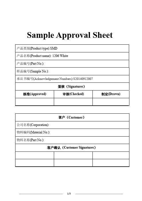
SMD 1206白色产品说明书
Ref. Standard 参考标准
JESD22-B106
JESD22-A104
Thermal Shock (冷热冲击)
JESD22-A106
Power temperature Cycling (高低温点亮循环测试)
High temperature Storage (高温储存) Low temperature Storage (低温储存) Lift Test (寿命测试) High Humidity Heat Lift Test (高温高湿老化)
5/8
Packaging Dimensions Specification(包装规格)
Notes:
1. Empty component pockets are sealed with top cover tape; 2. The maximum number of missing lamps is two; 3. The cathode is oriented towards the tape sprocket hole in accordance with ANSI/
2)Handwork soldering is only allowed once. We won’t take responsibility for more than that. 手工焊接只可进行一次,重复焊接不保证产品是否完好。
3)Avoid using sharp objects to compress products Colloidal Part directly. 避免使用尖锐的物体直接接触产品胶体部分。
JESD22-A105 JESD22-A103 JESD22-A119 JESD22-A108 JESD22-A101
THS1206IDA;THS1206CDA;THS1206CDAR;THS1206CDARG4;THS1206IDAR;中文规格书,Datasheet资料

ABSOLUTE MAXIMUM RATINGS
over operating free-air temperature range unless otherwise noted(1) THS1206 DGND to DVDD Supply voltage range Analog input voltage range Reference input voltage Digital input voltage range Operating virtual junction temperature range, TJ THS1206C Operating free-air free air temperature range, range TA THS1206I THS1206Q THS1206M Storage temperature range, Tstg BGND to BVDD AGND to AVDD –0.3 V to 6.5 V –0.3 V to 6.5 V –0.3 V to 6.5 V AGND –0.3 V to AVDD + 1.5 V –0.3 V + AGND to AVDD + 0.3 V –0.3 V to BVDD/DVDD + 0.3 V –55°C to 150°C 0°C to 70°C –40°C to 85°C –40°C to 125°C –55°C to 125°C –65°C to 150°C
Lead temperature 1,6 mm (1/16 inch) from case for 10 seconds 260°C (1) Stresses beyond those listed under “absolute maximum ratings” may cause permanent damage to the device. These are stress ratings only, and functional operation of the device at these or any other conditions beyond those indicated under “recommended operating conditions” is not implied. Exposure to absolute-maximum-rated conditions for extended periods may affect device reliability.
Littelfuse 1206大小快速作用熔断器说明书
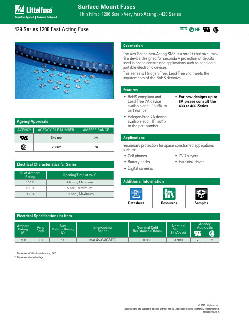
© 2015 Littelfuse, Inc. Specifications are subject to change without notice.Revised: 04/30/15DescriptionThe 429 Series Fast-Acting SMF is a small (1206 size) thin-film device designed for secondary protection of circuits used in space constrained applications such as hand-held portable electronic devices.This series is Halogen-Free, Lead-Free and meets the requirements of the RoHS directive.Agency ApprovalsElectrical Characteristics for Series Features• RoHS compliant andLead-Free 7A deviceavailable-add ‘L’ suffix topart number.• Halogen-Free 7A deviceavailable-add ‘HF’ suffixto the part number• For new designs up to5A please consult the433 or 466 Series ApplicationsElectrical Specifications by Item1. Measured at 10% of rated current, 25ºC.2. Measured at rated voltage.• Cell phones• Battery packs• Digital cameras• DVD players• Hard disk drives. Secondary protection for space constrained applications such as:Specifications are subject to change without notice. Application testing is strongly recommended.© 2015 Littelfuse, Inc.Specifications are subject to change without notice. Revised: 04/30/157ATIMEINSECONDSCURRENT IN AMPERES0.010.10.11110100101000.001 Soldering ParametersNote:1. Rerating depicted in this curve is in addition to the standard derating of 25% forcontinuous operation.Example:For continuous operation at 70 degrees celsius, the fuse should be deratedas follows:I = (0.75)(0.80)IRAT= (0.60)IRAT2. The temperature derating curve represents the nominal conditions. For questionsabout temperature derating curve, please consult Littelfuse technical supportfor assistance.© 2015 Littelfuse, Inc.Specifications are subject to change without notice.Revised: 04/30/15DimensionsREFLOW SOLDERRECOMMENDED PAD LAYOUTS1.52(.080")1.14Part Numbering SystemPackagingPart Marking System0429 007. WRM L HFSERIES AMP CodeQUANTITY CodeL = Lead-Free device and RoHS compliant device Refer to Amp Code Column of Electrical characteristics table WRM = 3000 pieces, Tape and Reel‘HF’ SUFFIXHALOGEN FREE ITEM。
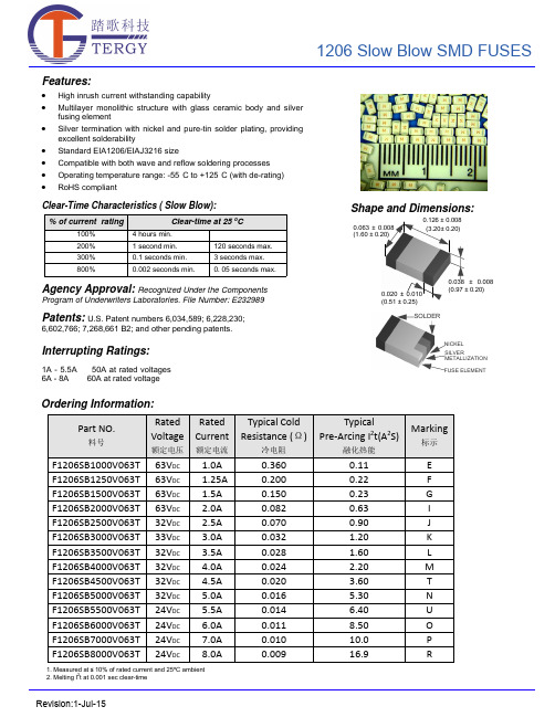
熔断保险丝1206SB封装型号参数规格书
Peak Temperature (TP)
Time within 5°C of actual peak
Temperature (tp)
Ramp-down Rate Time 25°C to peak Temperature (TP) Do not exceed
Pb-free assembly
150℃ 200℃ 60 – 120 seconds 3℃/second max.
1206 Slow Blow SMD FUSES
Features:
• High inrush current withstanding capability • Multilayer monolithic structure with glass ceramic body and silver
fusing element
0.063 ± 0.008 (1.60 ± 0.20)
0.126 ± 0.008 (3.20± 0.20)
0.020 ± 0.010 (0.51 ± 0.25)
0.038 ± 0.008 (0.97 ± 0.20)
SOLDER
NICKEL SILVER METALLIZATION
FUSE ELEMENT
Clear-Time (s)
100 10 1 0.1
0.01 0.001
1
Revision:18-Jul-15
1.0A 1.25A 1.5A 2.0A 2.5A 3.0A 3.5A 4.0A 4.5A 5.0A 5.5A 6.0A 7.0A 8.0A
1206 Slow Blow SMD FUSES
• Silver termination with nickel and pure-tin solder plating, providing
1206全彩贴片LED-1206全彩共阴LED规格书

SPECIFICATION FOR APPROVAL
客户 Customer:
客户品号 Customer P/N:
鑫光硕品号 Xgs Model:
规格 Specification :
XGS-PB3216UEUGUB-04-B SMD 1206 RGB共阴 20MA
制作 Prepared By:
审核 Checked By:
IF
25
Reverse Voltage
VR
5
Operating Temperature Range
Topr
-40℃~85℃
Storage Temperature Range
Tstg
-40℃~100℃
IFP condition: pulse width ≤1ms ,duty cycle ≤1/10
20
0/1
60cm/min,2 times
(2)Criteria of judging the damage
Item
Forward voltage Reverse current
Luminous intensity
Wave length
Appearance
Symbol VF IR IV
λD/λP /
◆ Applications:
Automotive and Telecommunication Flat backlight for LCD ,switch and symbol in telephone and fax General use for indicators
◆ Package Dimensions:
◆ Electrical Optical Characteristics(Ta=25℃)
BF862中文资料
1999 Jun 29
6
元器件交易网
Philips Semiconductors – a worldwide company
Argentina: see South America Australia: 34 Waterloo Road, NORTH RYDE, NSW 2113, Tel. +61 2 9805 4455, Fax. +61 2 9805 4466 Austria: Computerstr. 6, A-1101 WIEN, P.O. Box 213, Tel. +43 1 60 101 1248, Fax. +43 1 60 101 1210 Belarus: Hotel Minsk Business Center, Bld. 3, r. 1211, Volodarski Str. 6, 220050 MINSK, Tel. +375 172 20 0733, Fax. +375 172 20 0773 Belgium: see The Netherlands Brazil: see South America Bulgaria: Philips Bulgaria Ltd., Energoproject, 15th floor, 51 James Bourchier Blvd., 1407 SOFIA, Tel. +359 2 68 9211, Fax. +359 2 68 9102 Canada: PHILIPS SEMICONDUCTORS/COMPONENTS, Tel. +1 800 234 7381, Fax. +1 800 943 0087 China/Hong Kong: 501 Hong Kong Industrial Technology
PT1206BS 光敏三极管产品说明书

产品说明书1206贴片NPN光敏三极管PT1206BS ⏹描述PT1206BS是一款高速高灵敏度小型贴片NPN型光敏三极管1206封装,采用黑色环氧材料封装,产品适用于红外线的感光。
⏹特点●快速响应●高感光灵敏度●无铅环保●符合RoHS和REACH标准⏹应用●微型开关●计数器和分拣机●位置传感器●编码器●红外传感应用系统发射集集电极集电极标识建议回流焊焊盘尺寸注: 1. 所有尺寸单位位毫米(括号内单位为英寸) 2. 未标明误差的精度为± 0.2毫米(.008英寸) 3. 建议的焊盘尺寸仅供参考 请根据实际需要进行修改⏹封装尺寸⏹极限参数(Ta=25℃)参数名称符号参考值单位集电极-发射极电压V CEO 30V 发射极-集电极电压V ECO 5V 集电极电流Ic 20mA 焊接温度*1Tsol 260℃工作温度Topr -20~+85℃存储温度Tstg-40~+85℃说明:*1:焊接时间≦5seconds.Ambient Temperature Ta(°C)C o l l e c t o r P o w e rD i s s i p a t i o n (m W )40100020406080100-20-406080201008060200600Wavelength(nm)R e l a t i v e S p e c t r a l S e n s i t i v i t y (%)Ta=25°40700800900100011001200⏹光电参数(Ta=25℃)参数名称符号最小典型最大单位测试条件频谱范围λ0.5730--1100nm 感光峰值波长λP --940--nm 集电极–发射极击穿电压BV CEO30----V Ic=100μA,Ib=0发射极-集电极击穿电压BV ECO5----V Ic=100μA,Ib=0集电极暗电流I CEO ----100nA V CE =20V,H=0mw/cm2集电极-发射极饱和电压V CE (S )---0.4V Ic=2mA,I B =100μA 集电极电流I C (on)0.10.6--mAEe=1mW/cm2,V CE =5V 直流电流放大倍数H FE 1000--1800V CE =5V,IC=2mA 上升/下降时间t r /t f--15/15μS V CE =5V,I C =1mA R L =1000Ω⏹特性曲线图图.1集电极耗散功率与环境温度图.2相对频谱灵敏度300Ambient Temperature Ta(°C)R e l a t i v e C o l l e c t o r C u r r e n t (%)40608060100160Vce=5V204080120140Ee=1mW/cm 21020507025Ambient Temperature (°C)C o l l e c t o rD a r k C u r r e n t IC E O(n A )50751000.1110100Vce=20V 0.1Irradiance Ee(mW/cm )C o l l e c t o r C u r r e n t I c (m A )1100.01101010101010-1-2-3Vce=5VT =25 Ca °20Collector-Emitter Voltage V CE (V)C o l l e c t o r C u r r e n t I c (m A )12340.51.01.52.02.53.03.5Ee=0.5mW/cm2Ee=0.75mW/cm2Ee=1.0mW/cm2Ee=1.25mW/cm2Ee=1.5mW/cm2图.3相对集电极电流与环境温度图.4集电极电流与辐照度图.5集电极暗电流与环境温度图.6集电极电流与集射电压注: 1. 所有尺寸单位为毫米(英寸)发射极集电极注: 1. 所有尺寸单位为毫米(英寸)2. 未注明误差的尺寸为 ± 0.1mm(.004")⏹包装尺寸图⏹载带尺寸图(数量:3000个/盘)注意事项:1.我公司保留更改产品材料和以上说明书的权利,更改以上产品说明书恕不另行通知。
BF1205,135;中文规格书,Datasheet资料
(2)
g1 (a) g2
d (a) s d (b) R G1
(3)
8
g1 (b)
4
(4) (5) (6)
VGG
MGX431
0 0 1 2 3 4 VGG (V) 5
(1) ID (b); RG1 = 120 k. (2) ID (b); RG1 = 150 k. (3) ID (b); RG1 = 180 k.
(4) ID (a); RG1 = 180 k. (5) ID (a); RG1 = 150 k. (6) ID (a); RG1 = 120 k.
100
50
0 0 50 100 150 Ts (°C) 200
Fig.2 Power derating curve.
STATIC CHARACTERISTICS Tj = 25 C; per MOS-FET; unless otherwise specified. SYMBOL V(BR)DSS V(BR)G1-SS V(BR)G2-SS V(F)S-G1 V(F)S-G2 VG1-S(th) VG2-S(th) IDSX PARAMETER drain-source breakdown voltage gate-source breakdown voltage gate-source breakdown voltage forward source-gate voltage forward source-gate voltage gate-source threshold voltage gate-source threshold voltage drain-source current CONDITIONS MIN. MAX. 10 10 1.5 1.5 1 1.0 16 16 50 50 20 UNIT V V V V V V V V mA mA nA nA nA amp. a: VG1-S = VG2-S = 0 V; ID = 10 A 10 amp. b: VG1-S = VG2-S = 0 V; ID = 10 A 7 VGS = VDS = 0 V; IG1-S = 10 mA VGS = VDS = 0 V; IG2-S = 10 mA VG2-S = VDS = 0 V; IS-G1 = 10 mA VG1-S = VDS = 0 V; IS-G2 = 10 mA VDS = 5 V; VG2-S = 4 V; ID = 100 A VDS = 5 V; VG1-S = 5 V; ID = 100 A amp. a: VG2-S = 4 V; VDS = 5 V; RG1 = 150 k; note 1 amp. b: VG2-S = 4 V; VDS = 5 V; RG1 = 150 k; note 2 IG1-S IG2-S Note 1. RG1 connects gate 1 (b) to VGG = 0 V (see Fig.4). 2. RG1 connects gate 1 (b) to VGG = 5 V (see Fig.4). gate cut-off current gate cut-off current amp. a: VG1-S = 5 V; VG2-S = VDS = 0 V amp. b: VG1-S = 5 V; VG2-S = VDS = 0 V VG2-S = 4 V; VG1-S = VDS = 0 V 6 6 0.5 0.5 0.3 0.4 8 8
BFG135,115;中文规格书,Datasheet资料
1995 Seemiconductors
Product specification
NPN 7GHz wideband transistor
BFG135
THERMAL RESISTANCE 30 K/W
MAX. 1
UNIT A pF pF pF GHz dB dB mV mV dB
53
dB
1995 Sep 13
3
/
NXP Semiconductors
Product specification
lfpage
BFG135
4
1
Top view
2
3
MSB002 - 1
Fig.1 SOT223. QUICK REFERENCE DATA SYMBOL VCBO VCEO IC Ptot hFE fT GUM PARAMETER collector-base voltage collector-emitter voltage DC collector current total power dissipation DC current gain transition frequency maximum unilateral power gain up to Ts = 145 C (note 1) IC = 100 mA; VCE = 10 V; Tj = 25 C IC = 100 mA; VCE = 10 V; f = 1 GHz; Tamb = 25 C IC = 100 mA; VCE = 10 V; f = 500 MHz; Tamb = 25 C IC = 100 mA; VCE = 10 V; f = 800 MHz; Tamb = 25 C Vo output voltage open base CONDITIONS open emitter 80 MIN. 130 7 16 12 850 TYP. MAX. 25 15 150 1 GHz dB dB mV UNIT V V mA W
1206红光贴片灯珠规格书

1206红光贴片灯珠规格书1206 red SMD Specifications描述Description1206灯珠最大的优点在于性能稳定,性价比高.市面上用1206灯珠主要用于指示, LCD背光1206 lamp beads the biggest advantage is the stable performance, high cost performance. The market uses 1206 lamp beads mainly used for instructions, LCD backlight.特点Features产品具有亮度高,寿命长的优点,6000小时0光衰The product has the advantages of high brightness, long life, 6000 hours 0 light fa客户名称:CUSTOMER NAME: 经办者: 职称:DIRECTOR: TITLE: 客户料号:CUSTOMER PART NO.: 品名: 版本:PART NUMBER: YT1206ROS1-6200 REVISION: 2.0 发件日期: 回文日期: ISSUE DATE: 2014-11-4 RETURN DATE: / /一、谨致执事者:兹提供敝公司产品之有关详细规格及图面数据,敬请给予办理测试认定手续。
同时敬请送返一份附有贵公司签认之测试认定后之样品认定书。
We are please in sending you herewith our specification and drawings for your approval. Please return to us one copy “For Approval” with your approved signatures. 二、附件:ACCESSORY :□样品 □出货检验记录表 □封装尺寸图 □电气特性曲线□内部线路图 □焊性建议 □PAD 建议 □包装方式 三、客户意见栏 C USTOMER’S PROPOSAL□ AGREE 同意 (请于认可栏中签名) □ DISAGREE 不同意REASON 原因: 客户认可签章:CUSTOMER SIGNATURE:Features_3.2mmX1.6mm SMT LED, 0.90mm THICKNESS. _LOW POWER CONSUMPTION.DescriptionThe Hyper Red source color devices are made_WIDE VIEWING ANGLE._IDEAL FOR BACKLIGHT AND INDICATOR._VARIOUS COLORS AND LENS TYPES AVAILABLE. _PACKAGE: 3000PCS / REEL._RoHS COMPLIANT.Package DimensionsNotes:1. All dimensions are in millimeters (inches).2. Tolerance is ±0.1(0.004") unless otherwise noted.3.Specifications are subject to change without notice. Selection GuidePart No. Dice Lens TypeIv (mcd)@ 20mAViewingAngle Min. Typ. 2 θ 1/2YT1206ROS1-6200RED WATER CLEAR 70 150 120Note:1. θ1/2 is the angle from optical centerline where the luminous intensity is 1/2 the optical centerline value.Electrical / Optical Characteristics at T A=25°CSymbol Parameter Device Typ. Max. Units Test Conditionsλpeak Peak Wavelength RED617 625 nm IF=20mAλD Dominant Wavelength RED nm IF=20mA∆λ1/2 Spectral Line Half-width RED25 nm IF=20mAC Capacitance RED105 pF VF=0V;f=1MHzVF Forward Voltage RED 1.9 2.2 V IF=20mAIR Reverse Curren RED 2 uA VR = 7VRemarks:If special sorting is required (e.g. binning based on forward voltage, luminous intensity, or wavelength), the typicalaccuracy of the sorting process is as follows:1. Wavelength: +/-1nm2. Luminous Intensity: +/-15%3. Forward Voltage: +/-0.1VNote: Accuracy may depend on the sorting parametersAbsolute Maximum Ratings at T A=25°CParameter RED UnitsPower dissipation 75 mWDC Forward Current 30 mAPeak Forward Current [1] 80 mAReverse Voltage 5 VOperating/Storage Temperature -40°C To +85°CNote:1. 1/10 Duty Cycle, 0.1ms Pulse Width.E6C1206URAC1UDA可靠性RELIABILITY测试项目及结果Test Items and Results序号试验项目参考标准试验条件持续时间取样数接收水准(不合格数量/抽样总数)1 温度循环JEITAED-4701-40℃~25℃~100℃~循环100 回合50 0/5025℃30 分钟5 分钟30 分钟 5 分钟2 冷热冲击MIL-STD-202G-40℃~100℃循环500 回合50 0/50 15 分钟15 分钟3 高温储存JEITA ED-4701200 201 T a=100℃1000 小时50 0/504 低温储存JEITA ED-4701200 201T a=-40℃1000 小时50 0/505 常温寿命T a=25±5℃1000 小时500/50 试验I F=20mA6 高温高湿T a=60℃RH=85%1000 小时500/50 寿命试验I F=20mA7可焊性JEITA ED-4701 T sol=235℃±5℃,5 秒焊接一次,5 秒10 0/10 (回流焊)300 303 使用助焊剂8耐焊性JEITA ED-4701 T sol=260℃,10 秒焊接二次,每次10 秒10 0/10 (回流焊)300 301预处理:35℃95%RH96小时备准以上试验项目如与客户试验要求存在差异的或者特殊客户特殊要求的可根据实际情况按照客户的要求进行试作,客户未要求的按我司试验标准试作.不同产品使用不同电流进行测试5.注意事项Cautions(1) 焊接条件Soldering Conditions本产品最多只可回焊两次,且在首次回焊后须冷却至室温之后方可进行第二次回焊.Number of reflow process shall be less than 2 times and cooling process to normal temperature is required between first and Second soldering process.推荐焊接条件(Recommended soldering conditions)有铅回焊(Lead Solder)无铅回焊(Lead-Free Solder)Recommended Soldering Pattern(Units : mm)(2)静电Static Electricity触摸LED 时,推荐使用防静电手腕带或防静电手套.It is recommended that a wrist band or an anti-electrostatic glove be used when handling the LEDs.所有装置、设备、机器均应接地.All devices, equipment and machinery must be properly grounded.静电损坏的LED 会显示出异常特征:正向电压变低或在低电流时死灯.标准: IF=0.5mA 时, VF > 2.0V Damaged LEDs will show some unusual characteristics such as the forward voltage becomes lower, or the LEDs do not light at the low current. Criteria : (VF > 2.0V at IF=0.5mA)(3)防潮包装Moisture Proof Package使用防潮包装It is recommended that moisture proof package be used .(4)使用注意事项Cautions:4.1.在开包装之前,请先检查包装袋有无漏气,如果有漏气现象,请退回我司重新烘烤除湿包装后再使用。
1206 电阻通用规格书
o d u c t s p e c i f i c a t i o n – F e b r u a r y 6, 2013 V .5S u p e r s e d e s D a t e o f M a r . 06, 2003Y A G E O B R A N D o r d e r i n g c o d eGLOBAL PART NUMBER (PREFERRED )RC1206 X R - XX XXXX L(1) (2) (3) (4) (5) (6)(1) TOLERANCED = ±0.5% F = ±1%J = ±5% (for Jumper ordering, use code of J)(2) PACKAGING TYPER = Paper taping reel(3) TEMPERATURE COEFFICIENT OF RESISTANCE– = Base on spec(4) TAPING REEL07 = 7 inch dia. Reel 10 = 10 inch dia. Reel 13 = 13 inch dia. Reel(5) RESISTANCE VALUEThere are 2~4 digits indicated the resistor value. Letter R/K/M is decimal point, no need to mention the last zero after R/K/M, e.g.1K2, not 1K20.Detailed resistance rules show in table of “Resistance rule of global part number”.(6) DEFAULT CODELetter L is system default code for order only (Note)ORDERING INFORMATION - GLOBAL PART NUMBER & 12NC Both part numbers are identified by the series, size, tolerance, packing type, temperature coefficient, taping reel and resistance value.SCOPEThis specification describes RC1206 series chip resistors with lead-free terminations made by thick film process.APPLICATIONS● All general purpose applicationFEATURES● Halogen Free Epoxy●RoHS compliant- Products with lead freeterminations meet RoHS requirements- Pb-glass contained in electrodes,resistor element and glass are exempted by RoHS●Reducing environmentally hazardous wastes●High component and equipment reliability● Saving of PCB space●None forbidden-materials used in products/productionO RDERING EXAMPLEThe ordering code of a RC1206 chip resistor, value 56 X with ±1% tolerance, supplied in 7-inch tape reel is: RC1206FR-0756RL.NOTE1. All our RSMD products meet RoHS compliant and Halogen Free. "LFP" of the internal 2D reel label mentions "Lead Free Process"2. On customized label, "LFP" or specific symbol can be printedResistance rule of global part numberResistance code rule Example0R0R = Jumper XRXX(1 to 9.76 Ω) 1R = 1 Ω1R5 = 1.5 Ω9R76 = 9.76 ΩXXRX(10 to 97.6 Ω) 10R = 10 Ω97R6 = 97.6 ΩXXXR(100 to 976 Ω) 100R = 100 ΩXKXX(1 to 9.76 K Ω) 1K = 1,000 Ω9K76 = 9760 ΩXMXX(1 to 9.76 M Ω) 1M = 1,000,000 Ω9M76= 9,760,000 Ω12NC CODE2322 / 2350 XXX XXXXX L(1) (2) (3) (4)TYPE/ 1206 START IN (1) TOL. (%) RESISTANCERANGE PAPER / PE TAPE ON REEL (units) (2) 5,000 10,000/not preferred 20,000RC01 2322 ±5% 1 to 10 M Ω711 61xxx711 51xxx711 81xxx RC02 2322 ±1% 1 to 10 M Ω 724 6xxxx 724 7xxxx 724 8xxxxHRC01 2350±5% 11 to 22 M Ω 520 10xxx-- Jumper 2322 - 0 Ω 711 91032 711 91005711 92004P H Y C O M P B R A N D o r d e r i n g c o d e sBoth GLOBAL PART NUMBER (preferred) and 12NC (traditional) codes are acceptable to order Phycomp brand products. GLOBAL PART NUMBER (PREFERRED ) For detailed information of GLOBAL PART NUMBER and ordering example, please refer to page 2.Resistance decade (3) Last digit 0.01 to 0.0976 X 00.1 to 0.976 X 71 to 9.76 X 810 to 97.6 X 9100 to 976 X 11 to 9.76 K X 210 to 97.6 K X 3100 to 976 K X 41 to 9.76 M X 510 to 97.6 M X6Example: 0.02X = 0200 or 200 0.3 X = 3007 or 3071 X=1008 or 10833 K X = 3303 or 333 10 M X = 1006 or 106Last digit of 12NC(1) The resistors have a 12-digit ordering code starting with 2322 / 2350.(2) The subsequent 4 or 5 digits indicate the resistor tolerance andpackaging. (3) The remaining 4 or 3 digits represent the resistance value with thelast digit indicating the multiplier as shown in the table of “Last digit of 12NC”. (4) Letter L is system default code for order only (Note) O RDERING EXAMPLEThe ordering code of a RC02 resistor, value 56 X with ±1% tolerance, supplied in tape of 10,000 units per reel is: 232272465609L or RC1206FR-0756RL.NOTE1. All our RSMD products meet RoHS compliant and Halogen Free. "LFP" of the internal 2D reel label mentions "Lead Free Process"2. On customized label, "LFP" or specific symbol can be printedCONSTRUCTIONThe resistor is constructed on top of a high-grade ceramic body.Internal metal electrodes are added on each end to make the contacts to the thick film resistive element. The composition of the resistive element is a noble metal imbedded into a glass and covered by a second glass to prevent environment influences. The resistor is laser trimmed to the rated resistance value. The resistor is covered with a protective epoxy coat, finally the two external terminations (matte tin on Ni-barrier) are added. See fig.3DIMENSIONSTYPE RC1206L (mm)3.10 ± 0.10W (mm) 1.60 ± 0.10H (mm) 0.55 ± 0.10I 1 (mm) 0.45 ± 0.20I 2 (mm)0.40 ± 0.20T able 1O U T L I N E SMARKINGRC1206No markingFor further marking information, please refer to data sheet “Chip resistors marking”ELECTRICAL CHARACTERISTICS CHARACTERISTICS RC1206 1/4 WOperating Temperature Range –55 °C to +155 °CMaximum Working Voltage 200 V Maximum Overload Voltage 400 V Dielectric Withstanding Voltage500 VResistance Range5% (E24) 1 Ω to 22 M Ω1% (E24/E96) 1 Ω to 10 M Ω0.5% (E24/E96) 10 to 1 M ΩΩZero Ohm Jumper < 0.05 ΩTemperature Coefficient1 Ω ≤ R ≤ 10 Ω±200 ppm/°C ±200 ppm/°C 10 M Ω < R ≤ 22 M Ω10 Ω < R ≤ 10 M Ω±100 ppm/°CJumper CriteriaRated Current 2 A Maximum Current10 AFOOTPRINT AND SOLDERING PROFILESFor recommended footprint andsoldering profiles, please refer to data sheet “Chip resistors mounting”.T able 2PACKING STYLE AND PACKAGING QUANTITY PRODUCT TYPE PACKING STYLEREEL DIMENSIONQUANTITY PER REELRC1206 Paper Taping Reel (R) 7" (178 mm) 5,000 units10" (254 mm) 10,000 units13" (330 mm)20,000 unitsNOTE1. For paper tape and reel specification/dimensions, please see the special data sheet “Chip resistors packing”T able 3Packing style and packaging quantityFUNCTIONAL DESCRIPTIONP O W E R R A T I N GRC1206 rated power at 70°C is 1/4 W R ATED VOLTAGEThe DC or AC (rms) continuous working voltage corresponding to the rated power is determined by the following formula:V=R)(P Xor max. working voltage whichever is less WhereV=Continuous rated DC or AC (rms) working voltage (V) P=Rated power (W) R=Resistance value (X )TESTS AND REQUIREMENTSTEST TESTMETHOD PROCEDURE REQUIREMENTSTemperature Coefficient of Resistance (T.C.R.) IEC 60115-1 4.8 At +25/–55 °C and +25/+125 °C Refer to table 2Formula:T.C.R= ------------------------- ×106 (ppm/°C)Wheret1=+25 °C or specified room temperaturet2=–55 °C or +125 °C test temperatureR1=resistance at reference temperature in ohmsR2=resistance at test temperature in ohmsLife/Endurance IEC 60115-1 4.25.1 At 70±5 °C for 1,000 hours, RCWV applied for1.5 hours on, 0.5 hour off, still air required ±(1.0%+0.05 ) for 1%,Ω0.5% tol.±(3.0%+0.05 Ω) for 5% tol. <100 mΩ for JumperHigh Temperature Exposure/ Endurance at Upper Category Temperature IEC 60068-2-2 1,000 hours at 155±5 °C, unpowered ±(1.0%+0.05 ) for 1%,Ω0.5% tol.±(2.0%+0.05 Ω) for 5% tol.<50 mΩ for JumperMoisture Resistance MIL-STD-202G Method-106G Each temperature / humidity cycle is defined at 8hours, 3 cycles / 24 hours for 10d. with 25 °C /65 °C 95% R.H, without steps 7a & 7b,unpoweredParts mounted on test-boards, withoutcondensation on partsMeasurement at 24±2 hours after test conclusion±(0.5%+0.05 ) for 1%,Ω0.5% tol.±(2.0%+0.05 Ω) for 5% tol.<100 mΩ for JumperThermal Shock MIL-STD-202G Method-107G -55/+125 °CNumber of cycles required is 300. DevicesunmountedMaximum transfer time is 20 seconds. Dwell timeis 15 minutes. Air – Air ±(0.5%+0.05 ) for 1%,Ω0.5% tol.±(1%+0.05 Ω) for 5% tol.<50 mΩ for JumperShort Time Overload IEC60115-1 4.13 2.5 times of rated voltage or maximum overloadvoltage whichever is less for 5 sec at roomtemperature±(1.0%+0.05 ) for 1%,Ω0.5% tol.±(2.0%+0.05 Ω) for 5% tol.<50 mΩ for JumperNo visible damageT able 4 Test condition, procedure and requirementsR2–R1R1(t2–t1)TEST TESTMETHOD PROCEDURE REQUIREMENTSBoard Flex/ Bending IEC 60068-2-21 Chips mounted on a 90mm glass epoxy resinPCB (FR4)2 mm bendingBending time: 60±5 seconds±(1.0%+0.05 Ω)<50 mΩ for JumperNo visible damageLow Temperature Operation IEC 60068-2-1 The resistor shall be subjected to a DC ratedvoltage for 1.5 h-on, 0.5 h-off, at -55±3 °CThis constitutes shall be repeated for 96 hoursHowever the applied voltage shall not exceedthe maximum operating voltage±(0.5%+0.05 )Ωfor 1%,0.5% tol.±(1.0%+0.05 Ω) for 5% tol.No visible damageInsulation Resistance IEC 60115-1 4.6 Rated continuous overload voltage (RCOV)for 1 minuteType RC1206Voltage (DC) 100 V≥10 GΩDielectric Withstand Voltage IEC 60115-1 4.7 Maximum voltage (V rms) applied for 1 minuteType RC1206Voltage (AC) 500 V rmsNo breakdown or flashoverResistance to Solvent IPC/JEDEC J-STD-020D lsopropylalcohol (C3H7OH) followed bybrushingNo smearedNoise IEC 60115-1 4.12 Maximum voltage (Vrms) applied Resistors range ValueR < 100 Ω10 dB100 Ω≤ R < 1 KΩ20 dB1 KΩ≤ R < 10 KΩ30 dB10 KΩ≤ R < 100 KΩ40 dB100 KΩ≤ R < 1 MΩ46 dB1 MΩ≤ R ≤ 22 MΩ48 dBHumidity IEC 60115-1 4.37 Steady state for 1000 hours at 40 °C / 95% R.H.RCWV applied for 1.5 hours on and0.5 hour off ±(1.0%+0.05 ) for 1%,Ω0.5% tol.±(2.0%+0.05 Ω) for 5% tol. <100 mΩ for JumperTEST TESTMETHODPROCEDURE REQUIREMENTSIntermittent Overload IEC 60115-1 4.39 2.5 times of rated voltage or maximumoverload voltage whichever is less for 1 secondon and 25 seconds off; total 10,000 cycles±(1.0%+0.05 ) for 1%,Ω0.5% tol.±(2.0%+0.05 Ω) for 5% tol.<100 mΩ for JumperSolderability- Wetting IPC/JEDEC J-STD-002B test B Electrical Test not requiredMagnification 50XSMD conditions:1st step: method B, aging 4 hours at 155 °Cdry heat2nd step: leadfree solder bath at 245±3 °CDipping time: 3±0.5 seconds Well tinned (≥95% covered) No visible damage- Leaching IPC/JEDEC J-STD-002B test D Leadfree solder, 260 °C, 30 secondsimmersion timeNo visible damage- Resistance to Soldering Heat IEC 60068-2-58 Condition B, no pre-heat of samplesLeadfree solder, 260 °C, 10 secondsimmersion timeProcedure 2 for SMD: devices fluxed andcleaned with isopropanol±(0.5%+0.05 ) for 1%,Ω0.5% tol.±(1.0%+0.05 Ω) for 5% tol.<50 mΩ for JumperNo visible damageREVISION HISTORYREVISION DATE CHANGE NOTIFICATION DESCRIPTIONVersion 5 Feb 06, 2013 - -Marking updated-Add 0.5% toleranceVersion 4 Jul 02, 2009 - - Test Items and methods updated- Test requirements upgradedVersion 3 Jul 15, 2008 - - Change to dual brand datasheet that describe RC1206 with RoHS compliant- Description of "Halogen Free Epoxy" added- Define global part numberVersion 2 Sep 03, 2004 - - New datasheet for 1206 thick film 1% and 5% with lead-free terminations- Replace the 1206 part of pdf files: RC01_11_21_31_5, RC02_12_22_32_10,and HRC01_5_4- Test method and procedure updated- PE tape added (paper tape will be replaced by PE tape)- High ohmic products combined into standard products.“ Yageo reserves all the rights for revising the content of this datasheet without further notification, as long as the products itself are unchanged. Any product change will be announced by PCN.”國巨股份有限公司 新北市新店區寶橋路233之1號3樓 3F., 233-1, Baoqiao Rd., Xindian, Taipei 231, Taiwan t. +886.2.2917.7555 f. +886.2.2917.5078To remove AC0603/0805/1206 and RC0603/0805/1206 markingJanuary 16th , 2013Dear Customers,Yageo would like to announce that we will remove the Resistance Marking on Yageo’s R Chip case sizes 0603/0805/1206 products from March 1st 2013 for the purposes of reducing unnecessary chemical usages for environmental protections. To identify the product resistance value, the label on the reels has been serving and will continue serving the purposes. As for the product performance, features, specifications, manufacturing process and locations remain the same. That is to say the elimination of the resiatance marking on the product appearance has no impact on the product functionality and you can feel free to use it for your current applications.Yageo has provided no resistance marking on R Chip 0402/0201/01005 and on the entire MLCC family ever since. Given Yageo has been devoted to being eco-friendly, we decide to eliminate the marking on the R Chip of the sizes of 0603 and the above as soon as possible. There will be a short period of time that both types of the products, with marking and without marking, co exist while we are changing the production lines one by one. We highly appreciate your understanding that we may ship the products in parallel for some time. Yageo commits that we will make full efforts to shorten the overlapping period as much as we can.We truly appreciate being your business partner and serving your passivecomponent needs. If there are any questions, please feel free to contact Yageo’s sales offices.Sincerely Yours,Product Business Unit, R chip product marketing Yageo CorporationNotice Notice通知信取消AC及RC 0603/0805/1206系列字码印制2013年1月15日亲爱的客户,您好为了维护环境并减少非必要的化学原料使用,国巨在此通知您:自2013年3月1日起,将生产0603/0805/1206无字码印制的电阻。
- 1、下载文档前请自行甄别文档内容的完整性,平台不提供额外的编辑、内容补充、找答案等附加服务。
- 2、"仅部分预览"的文档,不可在线预览部分如存在完整性等问题,可反馈申请退款(可完整预览的文档不适用该条件!)。
- 3、如文档侵犯您的权益,请联系客服反馈,我们会尽快为您处理(人工客服工作时间:9:00-18:30)。
/
NXP Semiconductors
Product specification
Dual N-channel dual-gate MOS-FET
BF1206
CAUTION This product is supplied in anti-static packing to prevent damage caused by electrostatic discharge during transport and handling. ORDERING INFORMATION PACKAGE TYPE NUMBER NAME BF1206 DESCRIPTION plastic surface mounted package; 6 leads VERSION SOT363
DISCRETE SEMICONDUCTORS
DATA SHEET
handbook, halfpage
MBD128
BF1206 Dual N-channel dual-gate MOS-FET
Product specification 2003 Nov 17
/
NXP Semiconductors
Per MOS-FET; unless otherwise specified VDS ID yfs drain-source voltage drain current (DC) forward transfer admittance 6 30 48 44 2.9 2.2 1.9 2.0 V mA mS mS pF pF fF dBV dBV dB dB dB dB
Per MOS-FET unless otherwise specified V(BR)DSS V(BR)G1-SS V(BR)G2-SS V(F)S-G1 V(F)S-G2 VG1-S(th) VG2-S(th) IDSX drain-source breakdown voltage gate-source breakdown voltage gate-source breakdown voltage forward source-gate voltage forward source-gate voltage gate-source threshold voltage gate-source threshold voltage drain-source current 6 6 6 0.5 0.5 0.3 0.35 14 V V V V V V V mA mA nA nA
AMP a
BF1206
PINNING - SOT363 PIN 1 2 3 4 5 6 drain (b) source gate 1 (b) gate 1 (a) gate 2 drain (a) DESCRIPTION
handbook, halfpage
d (a) 5 4
g2
g1 (a)
6
AMP b
amp. b: 9 VG2-S = 4 V; VDS = 5 V; RG = 150 k note 1 IG1-S IG2-S Note 1. RG1 connects gate 1 to VGG = 5 V. gate cut-off current gate cut-off current VG1-S = 5 V; VG2-S = VDS = 0 VG2-S = 5 V; VG1-S = VDS = 0
50
0 0 50 100 1rating curve.
STATIC CHARACTERISTICS Tj = 25 C unless otherwise specified. SYMBOL PARAMETER CONDITIONS VG1-S = VG2-S = 0; ID = 10 A VGS = VDS = 0; IG1-S = 10 mA VGS = VDS = 0; IG2-S = 10 mA VG2-S = VDS = 0; IS-G1 = 10 mA VG1-S = VDS = 0; IS-G2 = 10 mA VDS = 5 V; VG2-S = 4 V; ID = 100 A VDS = 5 V; VG1-S = 5 V; ID = 100 A amp. a: VG2-S = 4 V; VDS = 5 V; RG = 91 k note 1 MIN. MAX. 10 10 1.5 1.5 1 1 23 17 50 20 UNIT
LIMITING VALUES In accordance with the Absolute Maximum Rating System (IEC 60134). SYMBOL PARAMETER CONDITIONS Ts 107 C; note 1 65 MIN. MAX. UNIT
2003 Nov 17
3
/
NXP Semiconductors
Product specification
Dual N-channel dual-gate MOS-FET
BF1206
handbook, halfpage
200
MLE257
Ptot (mW) 150
100
Per MOS-FET; unless otherwise specified VDS ID IG1 IG2 Ptot Tstg Tj Note 1. Ts is the temperature at the soldering point of the source lead. THERMAL CHARACTERISTICS SYMBOL Rth j-s PARAMETER thermal resistance from junction to soldering point VALUE 240 UNIT K/W drain-source voltage drain current (DC) gate 1 current gate 2 current total power dissipation storage temperature junction temperature 6 30 10 10 180 +150 150 V mA mA mA mW C C
1
2 Top view
3 d (b)
MAM480
s
g1 (b)
Marking code: L6-.
Fig.1 Simplified outline and symbol.
QUICK REFERENCE DATA SYMBOL PARAMETER CONDITIONS MIN. TYP. MAX. UNIT amp. a: ID = 18 mA amp. b: ID = 12 mA Cig1-s Crss Xmod input capacitance at gate 1 reverse transfer capacitance cross-modulation amp. a: ID = 18 mA; f = 1 MHz amp. b: ID = 12 mA; f = 1 MHz f = 1 MHz amp. a: input level for k = 1% at 40 dB AGC amp. b: input level for k = 1% at 40 dB AGC NF noise figure amp. a: f = 400 MHz; ID = 18 mA amp. b: f = 800 MHz; ID = 12 mA amp. a: f = 11 MHz; ID = 18 mA amp. b: f = 11 MHz; ID = 12 mA 2003 Nov 17 2 33 29 102 100 38 34 2.4 1.7 15 105 103 1.3 1.4 3 3.5
Product specification
Dual N-channel dual-gate MOS-FET
FEATURES Two low noise gain controlled amplifiers in a single package Superior cross-modulation performance during AGC High forward transfer admittance High forward transfer admittance to input capacitance ratio. APPLICATIONS Gain controlled low noise amplifiers for VHF and UHF applications with 5 V supply voltage, such as digital and analog television tuners. DESCRIPTION The BF1206 is a combination of two different dual gate MOS-FET amplifiers with shared source and gate 2 leads. The source and substrate are interconnected. Internal bias circuits enable DC stabilization and a very good cross-modulation performance during AGC. Integrated diodes between the gates and source protect against excessive input voltage surges. The transistor is encapsulated in SOT363 micro-miniature plastic package.
2003 Nov 17
4
/
NXP Semiconductors
