IRL540PBF中文资料
IRL540N中文资料

IRL540N®PD - 91495A5/13/98ParameterMax.UnitsI D @ T C = 25°C Continuous Drain Current, V GS @ 10V 36I D @ T C = 100°C Continuous Drain Current, V GS @ 10V 26A I DMPulsed Drain Current 120P D @T C = 25°C Power Dissipation 140W Linear Derating Factor 0.91W/°C V GS Gate-to-Source Voltage± 16V E AS Single Pulse Avalanche Energy 310mJ I AR Avalanche Current18A E AR Repetitive Avalanche Energy 14mJ dv/dt Peak Diode Recovery dv/dt 5.0V/ns T J Operating Junction and-55 to + 175T STGStorage Temperature RangeSoldering Temperature, for 10 seconds 300 (1.6mm from case )°CMounting torque, 6-32 or M3 srew10 lbf•in (1.1N•m)Absolute Maximum RatingsParameterTyp.Max.UnitsR θJC Junction-to-Case––– 1.1R θCS Case-to-Sink, Flat, Greased Surface 0.50–––°C/WR θJAJunction-to-Ambient–––62Thermal ResistanceDescriptionFifth Generation HEXFETs from International Rectifier utilize advanced processing techniques to achieve extremely low on-resistance per silicon area. This benefit, combined with the fast switching speed and ruggedized device design that HEXFET Power MOSFETs are well known for, provides the designer with an extremely efficient and reliable device for use in a wide variety of applications.The TO-220 package is universally preferred for all commercial-industrial applications at power dissipation levels to approximately 50 watts. The low thermal resistance and low package cost of the TO-220contribute to its wide acceptance throughout the industry.l Logic-Level Gate Drivel Advanced Process Technology l Dynamic dv/dt Ratingl 175°C Operating Temperature l Fast SwitchinglFully Avalanche RatedIRL540NIRL540NIRL540NIRL540NIRL540NIRL540NIRL540NNote: For the most current drawings please refer to the IR website at:/package/。
IRF540_03中文资料

1/8February 2003NEW DATASHEET ACCORDING TO PCN DSG/CT/1C16 MARKING: IRF540 &IRF540N-CHANNEL 100V - 0.055 Ω - 22A TO-220LOW GATE CHARGE STripFET™ II POWER MOSFETs TYPICAL R DS (on) = 0.055Ωs EXCEPTIONAL dv/dt CAPABILITY s 100% AVALANCHE TESTED s LOW GATE CHARGEsAPPLICATION ORIENTED CHARACTERIZATIONDESCRIPTIONThis MOSFET series realized with STMicroelectronics unique STripFET process has specifically been designed to minimize input capacitance and gate charge. It is therefore suitable as primary switch in advanced high-efficiency, high-frequency isolated DC-DC converters for Telecom and Computer applications. It is also intended for any applications with low gate drive requirements.APPLICATIONSs HIGH-EFFICIENCY DC-DC CONVERTERS s UPS AND MOTOR CONTROLTYPE V DSS R DS(on)I D IRF540100 V<0.077 Ω22 AOrdering InformationABSOLUTE MAXIMUM RATINGS(•) Pulse width limited by safe operating area.1) I SD ≤22A, di/dt ≤300A/µs, V DD ≤ V (BR)DSS , Tj ≤ T JMAX (2) Starting T j = 25 o C, I D = 12A, V DD = 30VSALES TYPEMARKINGPACKAGEPACKAGINGIRF540IRF540&TO-220TUBESymbol ParameterValue Unit V DS Drain-source Voltage (V GS = 0)100V V DGR Drain-gate Voltage (R GS = 20 k Ω)100V V GS Gate- source Voltage± 20V I D Drain Current (continuous) at T C = 25°C 22A I D Drain Current (continuous) at T C = 100°C 15A I DM (•)Drain Current (pulsed)88A P tot Total Dissipation at T C = 25°C 85W Derating Factor0.57W/°C dv/dt (1)Peak Diode Recovery voltage slope 9V/ns E AS (2)Single Pulse Avalanche Energy 220mJ T stg Storage Temperature-55 to 175°CT jMax. Operating Junction TemperatureIRF5402/8THERMAL DATAELECTRICAL CHARACTERISTICS (T case = 25 °C unless otherwise specified)OFFON (1)DYNAMICRthj-case Rthj-ambT lThermal Resistance Junction-case Thermal Resistance Junction-ambientMaximum Lead Temperature For Soldering PurposeMax Max Typ1.7662.5300°C/W °C/W °CSymbol ParameterTest ConditionsMin.Typ.Max.Unit V (BR)DSS Drain-sourceBreakdown Voltage I D = 250 µA, V GS = 0100V I DSSZero Gate VoltageDrain Current (V GS = 0)V DS = Max RatingV DS = Max Rating T C = 125°C 110µA µA I GSSGate-body Leakage Current (V DS = 0)V GS = ± 20V±100nASymbol ParameterTest ConditionsMin.Typ.Max.Unit V GS(th)Gate Threshold Voltage V DS = V GS I D = 250 µA 234V R DS(on)Static Drain-source On ResistanceV GS = 10 VI D = 11 A0.0550.077ΩSymbol ParameterTest ConditionsMin.Typ.Max.Unit g fs (*)Forward Transconductance V DS =25 VI D =11 A20S C iss C oss C rssInput Capacitance Output Capacitance Reverse Transfer CapacitanceV DS = 25V, f = 1 MHz, V GS = 087012552pF pF pF3/8IRF540SWITCHING ONSWITCHING OFFSOURCE DRAIN DIODEPulsed: Pulse duration = 300 µs, duty cycle 1.5 %.(•)Pulse width limited by safe operating area.Symbol ParameterTest ConditionsMin.Typ.Max.Unit t d(on)t r Turn-on Delay Time Rise TimeV DD = 50 VI D = 12 A R G =4.7 Ω V GS = 10 V (Resistive Load, Figure 3)6045ns ns Q g Q gs Q gdTotal Gate Charge Gate-Source Charge Gate-Drain ChargeV DD = 80 V I D = 22 A V GS = 10V3061041nC nC nCSymbol ParameterTest ConditionsMin.Typ.Max.Unit t d(off)t fTurn-off Delay Time Fall TimeV DD = 50 VI D = 12 A R G =4.7Ω, V GS = 10 V (Resistive Load, Figure 3)5020nsnsSymbol ParameterTest ConditionsMin.Typ.Max.Unit I SD I SDM (•)Source-drain CurrentSource-drain Current (pulsed)2288A A V SD (*)Forward On Voltage I SD = 22 AV GS = 01.3V t rr Q rr I RRMReverse Recovery Time Reverse Recovery Charge Reverse Recovery CurrentI SD = 22 Adi/dt = 100A/µs V DD = 30 V T j = 150°C (see test circuit, Figure 5)1003757.5ns nC AELECTRICAL CHARACTERISTICS (continued)IRF540IRF540IRF5406/8Fig. 3: Switching Times Test Circuits For ResistiveFig. 5: Test Circuit For Inductive Load Switching7/8IRF540DIM.mm.inch.MIN.TYP. MAX.MIN.TYP. TYP .A 4.4 4.60.1730.181C 1.23 1.320.0480.051D 2.40 2.720.0940.107E 0.490.700.0190.027F 0.610.880.0240.034F1 1.14 1.700.0440.067F2 1.14 1.700.0440.067G 4.95 5.150.1940.203G1 2.40 2.700.0940.106H21010.400.3930.409L216.400.645L328.901.137L413140.5110.551L5 2.65 2.950.1040.116L615.2515.750.6000.620L7 6.20 6.600.2440.260L9 3.50 3.930.1370.154DIA3.753.850.1470.151TO-220 MECHANICAL DATAIRF540Information furnished is believed to be accurate and reliable. However, STMicroelectronics assumes no responsibility for the consequences of use of such information nor for any infringement of patents or other rights of third parties which may result from its use. No license is granted by implication or otherwise under any patent or patent rights of STMicroelectronics. Specifications mentioned in this publication are subject to change without notice. This publication supersedes and replaces all information previously supplied. STMicroelectronics products are not authorized for use as critical components in life support devices or systems without express written approval of STMicroelectronics.The ST logo is registered trademark of STMicroelectronics® 2003 STMicroelectronics - All Rights ReservedAll other names are the property of their respective owners.STMicroelectronics GROUP OF COMPANIESAustralia - Brazil - Canada - China - Finland - France - Germany - Hong Kong - India - Israel - Italy - Japan - Malaysia - Malta - Morocco - Singapore - Spain - Sweden - Switzerland - United Kingdom - United States.8/8。
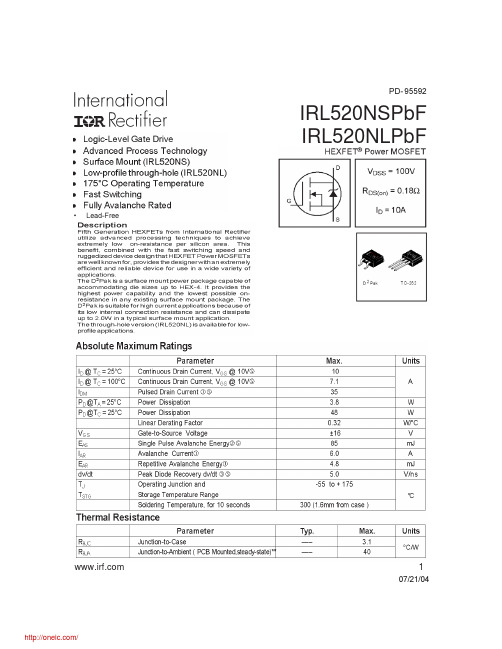
IRL520NSPBF;IRL520NLPBF;IRL520NSTRLPBF;中文规格书,Datasheet资料
26.40 (1.039) 24.40 (.961) 3
4
Data and specifications subject to change without notice.
IR WORLD HEADQUARTERS: 233 Kansas St., El Segundo, California 90245, USA Tel: (310) 252-7105 TAC Fax: (310) 252-7903 Visit us at for sales contact information. 07/04
AS S E MB LY L OT CODE
OR
INT E RNAT IONAL RE CT IFIE R L OGO PART NUMB ER F530S DAT E CODE P = DES IGNAT ES LEAD-F REE PRODU CT (OPT IONAL) YEAR 0 = 2000 WEEK 02 A = AS S E MB LY S IT E CODE AS S EMB L Y LOT CODE
8
/
IRL520NS/LPbF
TO-262 Package Outline
Dimensions are shown in millimeters (inches)
TO-262 Part Marking Information
E XAMPLE : T HIS IS AN IRL 3103L L OT CODE 1789 AS S E MB LE D ON WW 19, 1997 IN T HE AS S E MB LY LINE "C" Note: "P" in as s embly line pos ition indicates "Lead-F ree" INT E R NAT IONAL RE CT IF IE R LOGO AS S E MB LY LOT CODE PAR T NU MB E R
IRF540中文资料
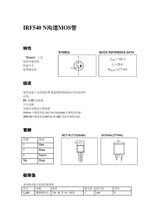
IRF540 N沟道MOS管特性‘Thrench’工艺低的导通内阻快速开关低热敏电阻综述使用沟渠工艺封装的N通道增强型场效应功率晶体管应用:DC到DC转换器开关电源电视及电脑显示器电源IRF540中提供的是SOT78(TO220AB)常规铅的包裹。
IRF540S中提供的是SOT404(D PAK)表面安装的包裹。
管脚管脚描述1 Gate2 Drain3 SourceTab Drain极限值系统绝对最大值依照限制值符号 参数 条件 最小值最大值 单位 V_DSS 漏源极电压 Tj= 25 ˚C to 175˚C - 100 VV_DGR V_GS I_D I_DM P_D Tj,Tsig漏门极电压 门源极电压 连续漏电流 脉冲漏电流 总功耗 操作点和存储温度Tj = 25 ˚C to 175˚C; RGS = 20 k Ω Tmb = 25 ˚C; VGS = 10 V Tmb = 100 ˚C; VGS = 10 V Tmb = 25 ˚C Tmb = 25 ˚C- - -- -- -55100 ±20 23 16 92 100 175V V A A A W ℃雪崩能量极限值符号 参数条件最小值最大值 单位AS E AS I非重复性雪崩能量最大非重复性雪崩电流Unclamped inductive load, IAS = 10 A; tp = 350 µs; Tj prior to avalanche = 25˚C; VDD ≤ 25 V; RGS = 50 Ω; VGS = 10 V; refer to fig:14- - 230 23mJ A热敏电阻符号参数条件最小值典型值 最大值 单位thj mb R - thj a R -安装底座交界处的热阻 周围环境热阻SOT78封装,自由空间SOT404封装,PCB 上- - -- 60 501.5 - -K/W K/W K/W电特性25℃ 除非另有说明 符号参数条件最小值 典型值 最大值单位 ()BR DSS V()GS TO V()DS ON R漏源极崩溃电压门阀电压漏源极导通电阻GS V =0V ;D I =0.25mATj = -55˚CDS V = ; ID = 1 mAGS V Tj = 175˚C Tj = -55˚CGS V = 10 V; ID = 17 ATj = 175˚C10089 21 - -- - 3 - - 49 132- - 4 - 6 77 193V V V V V m Ωm Ωfs g GSS I DSS I 向前跨导 门源极泄漏电流 0门极电压漏电流DS V =25V; D I =17A GS V =±20 V;DS V =0VVDS = 100 V; VGS = 0 VVDS=80V;VGS=0V;Tj= 175˚C 8.7 - - - 15.5 10 0.05 - - 100 10 250 S nA uA uA ()g tot Q gs Q gd Q 总共门极电荷 门源极电荷 门漏极电荷 ID = 17 A VDD = 80 V; VGS = 10 V- - - - - - 65 10 29 nC nC nC d on Tr T doff Tf T 开启延迟时间 开启上沿时间关闭延迟时间 关闭下沿时间 DD V = 50 V; D R = 2.2 Ω; DD V = 10 V; G R = 5.6 ΩResistive load- - - -8 39 26 24 - - - -ns ns ns ns d L d Ls L内部漏电感 内部漏电感内部源极电感Measured tab to centre of die Measured from drain lead to centre of die (SOT78 package only)Measured from source lead to source bond pad--- 3.5 4.5 7.5- - -nH nH nHiSS C oSS C rSS C输入电容 输出电容 反馈电容GS V = 0 V; S D V = 25 V; f = 1 MHz- - -890 139 831187 167 109pF pF pF反向二极管极限值及特性符号 参数条件最小值典型值最大值单位S I SM IDS V连续源极电流脉冲源极电流二极管正向电压F I =28A ; GS V =0V- - - - - 0.94 23 92 1.5 A A V t rrrr Q反向恢复之间反向恢复命令F I =17A ;=0V;GS V -d F I /dt=100A/us;=25VR V - -61 200- -ns nC底座温度-自然功率降低百分比图1:自然功率损耗底座温度-漏电流降低百分比图2 :自然持续漏电流漏源极电压-脉冲漏极电流峰值图3 :安全操作区域脉宽-瞬态热阻抗图4:瞬态热阻抗漏源极电压-漏极电流图5:典型输出特性漏极电流-漏源极导通阻抗图6:典型导通阻抗图7:典型传递特性图8:典型跨导图9:漏源极导通阻抗图10:门阀电压图11:阈漏极电流图12:典型电容值图13:典型的反向二极管电流图14:最大允许非重复性雪崩电流(IAS)和雪崩的时间。
irf540nspbf中文资料
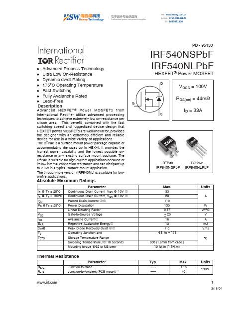
IRF540NSPbF IRF540NLPbFHEXFET ® Power MOSFET3/18/04 1Advanced HEXFET ® Power MOSFETs from International Rectifier utilize advanced processing techniques to achieve extremely low on-resistance per silicon area. This benefit, combined with the fast switching speed and ruggedized device design that HEXFET power MOSFETs are well known for, provides the designer with an extremely efficient and reliable device for use in a wide variety of applications.The D 2Pak is a surface mount power package capable of accommodating die sizes up to HEX-4. It provides the highest power capability and the lowest possible on-resistance in any existing surface mount package. The D 2Pak is suitable for high current applications because of its low internal connection resistance and can dissipate up to 2.0W in a typical surface mount application.The through-hole version (IRF540NL) is available for low-profile applications.lAdvanced Process Technology l Ultra Low On-Resistance l Dynamic dv/dt Ratingl 175°C Operating Temperature l Fast Switchingl Fully Avalanche Rated l Lead-Free DescriptionAbsolute Maximum RatingsParameterMax.UnitsI D @ T C= 25°C Continuous Drain Current, V GS @ 10V 33I D @ T C = 100°C Continuous Drain Current, V GS @ 10V 23A I DMPulsed Drain Current 110P D @T C = 25°C Power Dissipation 130W Linear Derating Factor 0.87W/°C V GS Gate-to-Source Voltage ± 20V I AR Avalanche Current16A E AR Repetitive Avalanche Energy 13mJ dv/dt Peak Diode Recovery dv/dt 7.0V/ns T J Operating Junction and-55 to + 175T STGStorage Temperature RangeSoldering Temperature, for 10 seconds 300 (1.6mm from case )°CMounting torque, 6-32 or M3 srew10 lbf•in (1.1N•m)D 2Pak IRF540NSPbF TO-262IRF540NLPbFParameterTyp.Max.UnitsR θJC Junction-to-Case––– 1.15R θJAJunction-to-Ambient (PCB mount)**–––40Thermal Resistance°C/WPD - 95130IRF540NS/LPbFSource-Drain Ratings and CharacteristicsRepetitive rating; pulse width limited bymax. junction temperature. (See fig. 11) Starting T J = 25°C, L =1.5mHR G = 25Ω, I AS = 16A. (See Figure 12)I SD ≤ 16A , di/d t ≤ 340A/µs, V DD ≤ V (BR)DSS , T J ≤ 175°CPulse width ≤ 400µs; duty cycle ≤ 2%.Notes:This is a typical value at device destruction and represents operation outside rated limits.This is a calculated value limited to T J = 175°C . Uses IRF540N data and test conditions.**When mounted on 1" square PCB (FR-4 or G-10 Material). For recommended footprint and soldering techniques refer to application note #AN-994Electrical Characteristics @ T J = 25°C (unless otherwise specified)IRF540NS/LPbF 3Fig 4. Normalized On-ResistanceVs. TemperatureIRF540NS/LPbFFig 8. Maximum Safe Operating AreaGate-to-Source VoltageDrain-to-Source Voltage Fig 7. Typical Source-Drain DiodeForward Voltage1101001000V DS , Drain-toSource Voltage (V)0.11101001000I D , D r a i n -t o -S o u r c e C u r r e n t (A )IRF540NS/LPbF 5Fig 11. Maximum Effective Transient Thermal Impedance, Junction-to-CaseCase TemperatureV V d(on)rd(off)fV DDFig 10a. Switching Time Test CircuitFig 10b. Switching Time WaveformsIRF540NS/LPbF6VDSCurrent Sampling ResistorsV GSFig 13b. Gate Charge Test CircuitFig 13a. Basic Gate Charge Waveform Fig 12b. Unclamped Inductive WaveformsI ASFig 12c. Maximum Avalanche EnergyVs. Drain CurrentV DDIRF540NS/LPbF 7Peak Diode Recovery dv/dt Test CircuitV DD* Reverse Polarity of D.U.T for P-ChannelV GS*** V GS = 5.0V for Logic Level and 3V Drive Devices Fig 14. For N-channel HEXFET ® power MOSFETsTO-262 Package OutlineIRF540NS/LPbFData and specifications subject to change without notice.This product has been designed and qualified for the industrial market.Qualification Standards can be found on IR’s Web site.IR WORLD HEADQUARTERS: 233 Kansas St., El Segundo, California 90245, USA Tel: (310) 252-7105TAC Fax: (310) 252-7903Visit us at for sales contact information .03/04344TRRFEED DIRECTION1.85 (.073)1.65 (.065)1.60 (.063)1.50 (.059)4.10 (.161)3.90 (.153)TRLFEED DIRECTION 10.90 (.429)10.70 (.421)16.10 (.634)15.90 (.626)1.75 (.069)1.25 (.049)11.60 (.457)11.40 (.449)15.42 (.609)15.22 (.601)4.72 (.136)4.52 (.178)24.30 (.957)23.90 (.941)0.368 (.0145)0.342 (.0135)1.60 (.063)1.50 (.059)13.50 (.532)12.80 (.504)330.00(14.173) MAX.27.40 (1.079)23.90 (.941)60.00 (2.362) MIN.30.40 (1.197) MAX.26.40 (1.039)24.40 (.961)NOTES :1. COMFORMS TO EIA-418.2. CONTROLLING DIMENSION: MILLIMETER.3. DIMENSION MEASURED @ HUB.4. INCLUDES FLANGE DISTORTION @ OUTER EDGE.D 2Pak Tape & Reel InfomationDimensions are shown in millimeters (inches)/package/。
IRF540中文资料
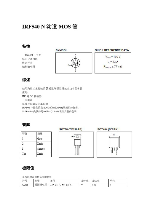
特性
‘Thrench’工艺 低的导通内阻 快速开关 低热敏电阻
综述
使用沟渠工艺封装的 N 通道增强型场效应功率晶体管 应用: DC 到 DC 转换器 开关电源 电视及电脑显示器电源 IRF540 中提供的是 SOT78(TO220AB)常规铅的包裹。 IRF540S中提供的是SOT404(D PAK)表面安装的包裹。
热敏电阻
符号 参数
安装底座交界 处的热阻 周围环境热阻
条件
最小值 -
典型值 60 50
最大值 1.5 -
单位 K/W K/W K/W
Rthj mb Rthj a
SOT78 封装,自由空间 SOT404 封装,PCB 上
-
电特性
25℃ 除非另有说明 符号 参数 漏源极崩溃电压 条件 最小值 100 Tj = -55˚C 门阀电压 89 2 Tj = 175˚C Tj = -55˚C 漏源极导通电阻 1 Tj = 175˚C 典型值 3 49 132 最大值 4 6 77 193 单位 V V V V V mΩ mΩ
-
Ls
内部源极电感
Measured from source lead to source bond pad
-
7.5
-
nH
CiSS CoSS CrSS
输入电容 输出电容 反馈电容
VGS = 0 V; VDS = 25 V; f = 1 MHz
-
890 139 83
1187 167 109
pF pF pF
反向二极管极限值及特性
符号
参数 连续源极电流 脉冲源极电流 二极管正向电压 反向恢复之间 反向恢复命令
IRF540中文数据手册知识讲解

I R F540中文数据手册
IRF540 N沟道MOS管
特性
‘Thrench’工艺
低的导通内阻
快速开关
低热敏电阻
综述
使用沟渠工艺封装的N通道增强型场效应功率晶体管应用:
DC到DC转换器
开关电源
电视及电脑显示器电源
IRF540中提供的是SOT78(TO220AB)常规铅的包裹。
IRF540S中提供的是SOT404(D PAK)表面安装的包裹。
管脚
管脚描述
1 Gate
2 Drain
3 Source
Tab Drain
极限值
雪崩能量极限值
热敏电阻
电特性
25℃除非另有说明
反向二极管极限值及特性
底座温度-自然功率降低百分比
图1:自然功率损耗
底座温度-漏电流降低百分比
图2 :自然持续漏电流
漏源极电压-脉冲漏极电流峰值
图3 :安全操作区域
脉宽-瞬态热阻抗
图4:瞬态热阻抗
漏源极电压-漏极电流
图5:典型输出特性
漏极电流-漏源极导通阻抗
图6:典型导通阻抗
图7:典型传递特性
图8:典型跨导
图9:漏源极导通阻抗
图10:门阀电压
图11:阈漏极电流
图12:典型电容值
图13:典型的反向二极管电流
图14:最大允许非重复性雪崩电流(IAS)和雪崩的时间。
IRF540中文资料_数据手册_参数
1500
1000 500 0 1
Coss
Crss
10
100
VDS , Drain-to-Source Voltage (V)
Fig 5. Typical Capacitance Vs. Drain-to-Source Voltage
Parameter Drain-to-Source Breakdown Voltage Breakdown Voltage Temp. Coefficient Static Drain-to-Source On-Resistance Gate Threshold Voltage Forward Transconductance
Thermal Resistance
RθJC RθCS RθJA
Parameter Junction-to-Case Case-to-Sink, Flat, Greased Surface Junction-to-Ambient
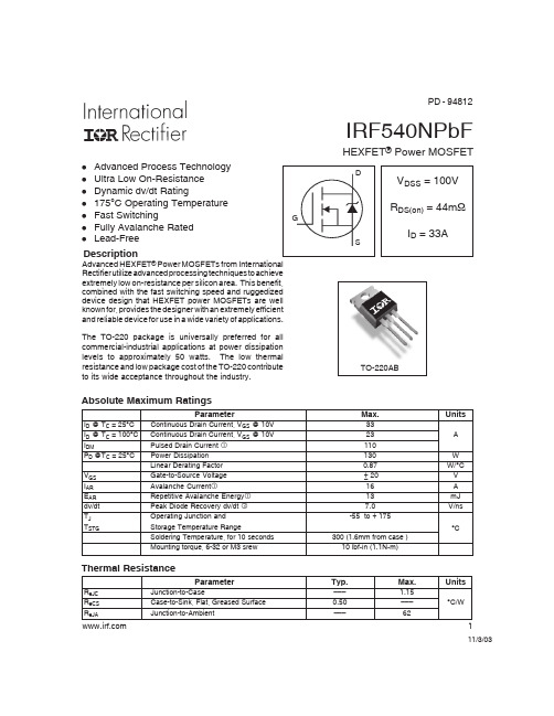
PD - 94812
IRF540NPbF
HEXFET® Power MOSFET
The TO-220 package is universally preferred for all commercial-industrial applications at power dissipation levels to approximately 50 watts. The low thermal resistance and low package cost of the TO-220 contribute to its wide acceptance throughout the industry.
1A)
TJ = 25°C 100
irf540
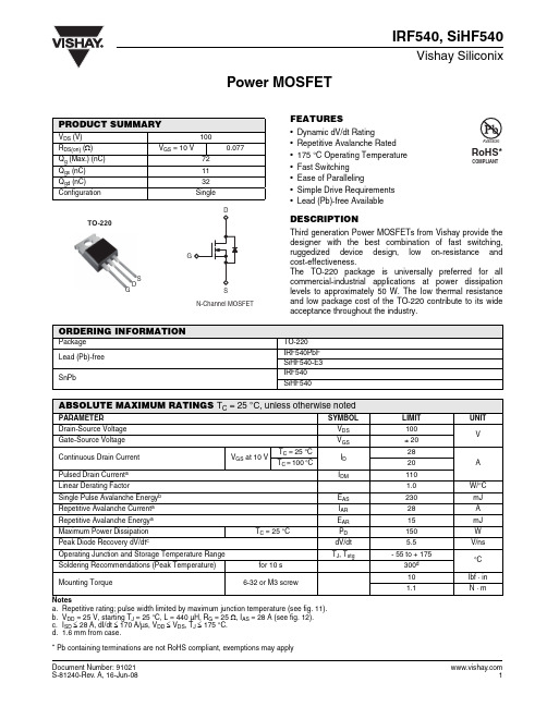
Power MOSFETIRF540, SiHF540Vishay SiliconixFEATURES•Dynamic dV/dt Rating•Repetitive Avalanche Rated •175 °C Operating Temperature •Fast Switching •Ease of Paralleling•Simple Drive Requirements •Lead (Pb)-free AvailableDESCRIPTIONThird generation Power MOSFETs from Vishay provide the designer with the best combination of fast switching,ruggedized device design, low on-resistance and cost-effectiveness.The TO-220 package is universally preferred for all commercial-industrial applications at power dissipation levels to approximately 50 W. The low thermal resistance and low package cost of the TO-220 contribute to its wide acceptance throughout the industry.Notesa.Repetitive rating; pulse width limited by maximum junction temperature (see fig. 11).b.V DD = 25 V, starting T J = 25 °C, L = 440 µH, R G = 25 Ω, I AS = 28 A (see fig. 12).c.I SD ≤ 28 A, dI/dt ≤ 170 A/µs, V DD ≤ V DS , T J ≤ 175 °C.d. 1.6 mm from case.PRODUCT SUMMARYV DS (V)100R DS(on) (Ω)V GS = 10 V0.077Q g (Max.) (nC)72Q gs (nC)11Q gd (nC)32ConfigurationSingleTO-220GDSORDERING INFORMATIONPackage TO-220Lead (Pb)-free IRF540PbF SiHF540-E3 SnPbIRF540SiHF540ABSOLUTE MAXIMUM RATINGS T C = 25 °C, unless otherwise notedARAMETER SYMBOL LIMIT UNIT Drain-Source Voltage V DS100VGate-Source Voltage V GS ± 20 Continuous Drain Current V GS at 10 VT C = 25 °C I D28A T C = 100 °C20Pulsed Drain Current a I DM 110Linear Derating Factor1.0W/°C Single Pulse Avalanche Energy b E AS 230mJ Repetitive Avalanche Current a I AR 28 A Repetitive Avalanche Energy a E AR 15mJ Maximum Power Dissipation T C = 25 °CP D 150WPeak Diode Recovery dV/dt cdV/dt 5.5V/ns Operating Junction and Storage Temperature Range T J , T stg- 55 to + 175°C Soldering Recommendations (Peak Temperature)for 10 s 300d Mounting Torque6-32 or M3 screw10 lbf · in 1.1N · m * Pb containing terminations are not RoHS compliant, exemptions may applyIRF540, SiHF540Vishay SiliconixNotesa.Repetitive rating; pulse width limited by maximum junction temperature (see fig. 11).b.Pulse width ≤ 300 µs; duty cycle ≤ 2 %.THERMAL RESISTANCE RATINGSARAMETER SYMBOL TY.MAX.UNITMaximum Junction-to-Ambient R thJA -62°C/W Case-to-Sink, Flat, Greased Surface R thCS 0.50-Maximum Junction-to-Case (Drain)R thJC- 1.0IRF540, SiHF540Vishay Siliconix TYPICAL CHARACTERISTICS 25 °C, unless otherwise notedFig. 1 - Typical Output Characteristics, T C= 25 °C Fig. 2 - Typical Output Characteristics, T C= 175 °CFig. 3 - Typical Transfer CharacteristicsFig. 4 - Normalized On-Resistance vs. TemperatureIRF540, SiHF540 Vishay SiliconixFig. 5 - Typical Capacitance vs. Drain-to-Source VoltageFig. 6 - Typical Gate Charge vs. Gate-to-Source VoltageFig. 7 - Typical Source-Drain Diode Forward VoltageFig. 8 - Maximum Safe Operating AreaIRF540, SiHF540Vishay SiliconixFig. 9 - Maximum Drain Current vs. Case TemperatureFig. 10a - Switching Time Test CircuitFig. 10b - Switching Time WaveformsFig. 11 - Maximum Effective Transient Thermal Impedance, Junction-to-CaseFig. 12a - Unclamped Inductive Test CircuitFig. 12b - Unclamped Inductive WaveformsIRF540, SiHF540Vishay SiliconixFig. 12c - Maximum Avalanche Energy vs. Drain CurrentFig. 13a - Basic Gate Charge WaveformFig. 13b - Gate Charge Test CircuitIRF540, SiHF540Vishay Siliconix Array Fig. 14 - For N-ChannelVishay Siliconix maintains worldwide manufacturing capability. Products may be manufactured at one of several qualified locations. Reliability data for Silicon Technology and Package Reliability represent a composite of all qualified locations. For related documents such as package/tape drawings, part marking, andreliability data, see /ppg?91021.Disclaimer Legal Disclaimer NoticeVishayAll product specifications and data are subject to change without notice.Vishay Intertechnology, Inc., its affiliates, agents, and employees, and all persons acting on its or their behalf (collectively, “Vishay”), disclaim any and all liability for any errors, inaccuracies or incompleteness contained herein or in any other disclosure relating to any product.Vishay disclaims any and all liability arising out of the use or application of any product described herein or of any information provided herein to the maximum extent permitted by law. The product specifications do not expand or otherwise modify Vishay’s terms and conditions of purchase, including but not limited to the warranty expressed therein, which apply to these products.No license, express or implied, by estoppel or otherwise, to any intellectual property rights is granted by this document or by any conduct of Vishay.The products shown herein are not designed for use in medical, life-saving, or life-sustaining applications unless otherwise expressly indicated. Customers using or selling Vishay products not expressly indicated for use in such applications do so entirely at their own risk and agree to fully indemnify Vishay for any damages arising or resulting from such use or sale. Please contact authorized Vishay personnel to obtain written terms and conditions regarding products designed for such applications.Product names and markings noted herein may be trademarks of their respective owners.。
IRFR5505PBF中文资料
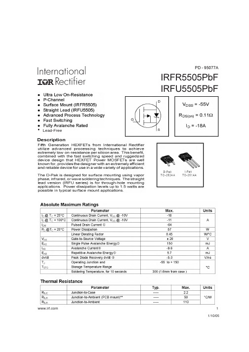
Dimensions are shown in millimeters (inches)
TR TRR TRL
16.3 ( .641 ) 15.7 ( .619 )
16.3 ( .641 ) 15.7 ( .619 )
12.1 ( .476 ) 11.9 ( .469 )
EXAMPLE: THIS IS AN IRF U120 WIT H AS SEMBLY LOT CODE 5678 ASS EMBLE D ON WW 19, 1999 IN T HE AS SEMBLY LINE "A" Note: "P" in as s embly line pos ition indicates "Lead-Free" PART NUMBE R INTE RNAT IONAL RECTIF IER LOGO
7
元器件交易网
IRFR/U5505PbF
D-Pak (TO-252AA) Package Outline
Dimensions are shown in millimeters (inches)
D-Pak (TO-252AA) Part Marking Information
13 INCH
16 mm NOTES : 1. OUTLINE CONFORMS TO EIA-481.
Data and specifications subject to change without notice.
IR WORLD HEADQUARTERS: 233 Kansas St., El Segundo, California 90245, USA Tel: (310) 252-7105 TAC Fax: (310) 252-7903 Visit us at for sales contact information.1/05 10
IRFR5505TRPBF中文资料

元器件交易网
Note: For the most current drawings please refer to the IR website at: /package/
Driver Gate Drive P.W. Period D= P.W. Period VGS=10V
D.U.T. ISD Waveform Reverse Recovery Current Body Diode Forward Current di/dt D.U.T. VDS Waveform Diode Recovery dv/dt
IRF U120 919A 56 78
AS SEMBLY LOT CODE
DAT E CODE YEAR 9 = 1999 WEE K 19 LINE A
OR
INT ERNAT IONAL RECT IFIER LOGO PART NUMBER
IRFU120 56 78
AS SEMB LY LOT CODE
7
元器件交易网
IRFR/U5505PbF
D-Pak (TO-252AA) Package Outline
Dimensions are shown in millimeters (inches)
D-Pak (TO-252AA) Part Marking Information
DAT E CODE P = DES IGNAT ES LEAD-FREE PRODUCT (OPT IONAL) YEAR 9 = 1999 WEEK 19 A = ASS EMBLY SIT E CODE
9
元器件交易网
IRFR/U5505PbF
VDD
Re-Applied Voltage Inductor Curent
IRFR5305-IRFR1205中文资料描述

漏极至源极电压(Vdss)
55V
Id时的Vgs(th)(最大)
4V @ 250µA
闸电荷(Qg) @ Vgs
65nC @ 10V
电流-连续漏极(Id) @25°C
44A
在Vds时的输入电容(Ciss)
1300pF @ 25V
功率-最大
107W
安装类型
表面贴装
BC817-16中文资料描述:TRANSISTOR NPN 45V 310MW SOT23-3
63nC @ 10V
电流-连续漏极(Id) @25°C
31A
在Vds时的输入电容(Ciss)
1200pF @ 25V
功率-最大
110W
安装类型
表面贴装
IRFR1205中文资料描述:MOSFET N-CH 55V44ADPAK
FET型
MOSFET N通道,金属氧化物
FET特点
标准型
开态Rds(最大)@ Id, Vgs @(Ic)(最大)
800mA
电压-集电极发射极击穿(最大)
45V
Ib、Ic条件下的Vce饱和度(最大)
700mV @ 50mA, 500mA
电流-集电极截止(最大)
100nA
在某Ic、Vce时的最小直流电流增益(hFE)
100 @ 100mA, 1V
功率-最大
310mW
频率-转换
IRFR5305PBF中文资料描述:MOSFET P-CH 55V31ADPAK
FET型
MOSFET P通道,金属氧化物
FET特点
标准型
开态Rds(最大)@ Id, Vgs @25°C
65毫欧@16A, 10V
IRFI540NPBF;中文规格书,Datasheet资料

HEXFET ® Power MOSFETIRFI540NPbFPD - 9483311/13/03l Advanced Process Technology l Isolated Packagel High Voltage Isolation = 2.5KVRMS l Sink to Lead Creepage Dist. = 4.8mm l Fully Avalanche Rated lLead-FreeAbsolute Maximum RatingsDescriptionFifth Generation HEXFETs from International Rectifier utilize advanced processing techniques to achieve the lowest possible on-resistance per silicon area. This benefit,combined with the fast switching speed and ruggedized device design that HEXFET Power MOSFETs are well known for, provides the designer with an extremely efficient device for use in a wide variety of applications.The TO-220 Fullpak eliminates the need for additional insulating hardware in commercial-industrial applications.The moulding compound used provides a high isolation capability and a low thermal resistance between the tab and external heatsink. This isolation is equivalent to using a 100 micron mica barrier with standard TO-220 product.The Fullpak is mounted to a heatsink using a single clip or by a single screw fixing.IRFI540NPbFSource-Drain Ratings and CharacteristicsNotes:Repetitive rating; pulse width limited bymax. junction temperature. ( See fig. 11 )V DD = 25V, starting T J = 25°C, L = 2.0mH R G = 25Ω, I AS = 16A. (See Figure 12) t=60s, =60HzI SD ≤ 16A, di/dt ≤ 210A/µs, V DD ≤ V (BR)DSS ,T J ≤ 175°CUses IRF540N data and test conditionsPulse width ≤ 300µs; duty cycle ≤ 2%.IRFI540NPbFFig 1. Typical Output Characteristics Fig 3. Typical Transfer CharacteristicsFig 4. Normalized On-ResistanceVs. TemperatureFig 2. Typical Output Characteristics11010010000.1110100I , D r a i n -t o -S o u r c e C u r r e n t (A )DV , Drain-to-Source Voltage (V)DS11010010000.1110100I , D r a i n -t o -S o u r c e C u r r e n t (A )DV , Drain-to-Source Voltage (V)DS110100100045678910GSV , Gate-to-Source Voltage (V)D I , D r a i n -t o -S o u r c e C u r r e n t (A )0.00.51.01.52.02.53.0-60-40-2020406080100120140160180JT , Junction Temperature (°C)R, D r a i n -t o -S o u r c e O n R e s i s t a n c e D S (o n)(N o r m a l i z e d )IRFI540NPbFFig 7. Typical Source-Drain Diode Forward VoltageFig 5. Typical Capacitance Vs.Drain-to-Source Voltage Fig 8. Maximum Safe Operating AreaFig 6. Typical Gate Charge Vs.Gate-to-Source Voltage04008001200160020002400110100C , C a p a c i t a n c e (p F )DSV , Drain-to-Source Voltage (V)04812162020406080100Q , Total Gate Charge (nC)GV , G a t e -t o -S o u r c e V o l t a g e (V )G S1010010000.40.81.21.62.0V , Source-to-Drain Voltage (V)I , R e v e r s e D r a i n C u r r e n t (A )SD S D 11010010001101001000V , Drain-to-Source Voltage (V)DSI , D r a i n C u r r e n t (A )DIRFI540NPbFFig 9. Maximum Drain Current Vs.Case TemperatureFig 10a.Switching Time Test CircuitV V d(on)rd(off)fFig 10b. Switching Time WaveformsFig 11. Maximum Effective Transient Thermal Impedance, Junction-to-CaseV DDIRFI540NPbFFig 12a. Unclamped Inductive Test CircuitFig 12b.Unclamped Inductive WaveformsVDDV I ASV10 VDSCurrent Sampling ResistorsFig 13a. Basic Gate Charge Waveform Fig 12c. Maximum Avalanche EnergyVs. Drain CurrentFig 13b. Gate Charge Test Circuit100200300400500600700255075100125150175JE , S i n g l e P u l s e A v a l a n c h e E n e r g y(m J )AS Starting T , Junction Temperature (°C)IRFI540NPbFPeak Diode Recovery dv/dt Test CircuitV DD Array* V GS = 5V for Logic Level DevicesFig 14. For N-Channel HEXFETS233 Kansas St., El Segundo, California 90245, USA Tel: (310) 252-7105TAC Fax: (310) 252-7903 Visit us at for sales contact information.11/03Note: For the most current drawings please refer to the IR website at:/package/分销商库存信息: IRIRFI540NPBF。
IRFPC40PBF中文资料

Power MOSFETIRFPC40, SiHFPC40Vishay SiliconixFEATURES•Dynamic dV/dt Rating •Repetitive Avalanche Rated •Isolated Central Mounting Hole •Fast Switching •Ease of Paralleling •Simple Drive Requirements •Lead (Pb)-free AvailableDESCRIPTIONThird generation Power MOSFETs from Vishay provide the designer with the best combination of fast switching,ruggedized device design, low on-resistance and cost-effectiveness.The TO-247 package is preferred for commercial-industrial applications where higher power levels preclude the use of TO-220 devices. The TO-247 is similar but superior to the earlier TO-218 package because of its isolated mounting hole. It also provides greater creepage distance between pins to meet the requirements of most safety specifications.Notesa.Repetitive rating; pulse width limited by maximum junction temperature (see fig. 11).b.V DD = 50 V, starting T J = 25 °C, L = 16 mH, R G = 25 Ω, I AS = 6.8 A (see fig. 12).c.I SD ≤ 6.8 A, dI/dt ≤ 80 A/µs, V DD ≤ V DS , T J ≤ 150 °C.d. 1.6 mm from casePRODUCT SUMMARYV DS (V)600R DS(on) (Ω)V GS = 10 V1.2Q g (Max.) (nC)60Q gs (nC)8.3Q gd (nC)30ConfigurationSingleTO-247GDSORDERING INFORMATIONPackage TO-247Lead (Pb)-free IRFPC40PbF SiHFPC40-E3 SnPbIRFPC40SiHFPC40ABSOLUTE MAXIMUM RATINGS T C = 25 °C, unless otherwise notedARAMETER SYMBOL LIMIT UNIT Drain-Source Voltage V DS600VGate-Source Voltage V GS ± 20 Continuous Drain Current V GS at 10 VT C = 25 °C I D6.8A T C = 100 °C4.3Pulsed Drain Current a I DM 27Linear Derating Factor1.2W/°C Single Pulse Avalanche Energy b E AS 410mJ Maximum Power Dissipation T C = 25 °CP D 150WPeak Diode Recovery dV/dt cdV/dt 3.0V/ns Operating Junction and Storage Temperature Range T J , T stg- 55 to + 150°C Soldering Recommendations (Peak Temperature)for 10 s 300d Mounting Torque6-32 or M3 screw10 lbf · in 1.1N · m * Pb containing terminations are not RoHS compliant, exemptions may apply元器件交易网IRFPC40, SiHFPC40Vishay SiliconixNotesa.Repetitive rating; pulse width limited by maximum junction temperature (see fig. 11).b.Pulse width ≤ 300 µs; duty cycle ≤ 2 %.THERMAL RESISTANCE RATINGSARAMETER SYMBOL TY.MAX.UNIT Maximum Junction-to-Ambient R thJA -40°C/WCase-to-Sink, Flat, Greased Surface R thCS 0.24-Maximum Junction-to-Case (Drain)R thJC-0.83元器件交易网元器件交易网Vishay SiliconixIRFPC40, SiHFPC40 Vishay SiliconixFig. 5 - Typical Capacitance vs. Drain-to-Source VoltageFig. 7 - Typical Source-Drain Diode Forward Voltage元器件交易网IRFPC40, SiHFPC40Vishay SiliconixFig. 9 - Maximum Drain Current vs. Case TemperatureFig. 10a - Switching Time Test CircuitFig. 10b - Switching Time WaveformsFig. 11 - Maximum Effective Transient Thermal Impedance, Junction-to-Case元器件交易网IRFPC40, SiHFPC40Vishay SiliconixFig. 12a - Unclamped Inductive Test CircuitFig. 12b - Unclamped Inductive WaveformsFig. 12c - Maximum Avalanche Energy vs. Drain CurrentFig. 13a - Basic Gate Charge WaveformFig. 13b - Gate Charge Test Circuit元器件交易网IRFPC40, SiHFPC40Vishay SiliconixFig.14 - For N-ChannelVishay Siliconix maintains worldwide manufacturing capability. Products may be manufactured at one of several qualified locations. Reliability data for Silicon Technology and Package Reliability represent a composite of all qualified locations. For related documents such as package/tape drawings, part marking, and reliability data, see /ppg?91240.元器件交易网Disclaimer Legal Disclaimer NoticeVishayAll product specifications and data are subject to change without notice.Vishay Intertechnology, Inc., its affiliates, agents, and employees, and all persons acting on its or their behalf (collectively, “Vishay”), disclaim any and all liability for any errors, inaccuracies or incompleteness contained herein or in any other disclosure relating to any product.Vishay disclaims any and all liability arising out of the use or application of any product described herein or of any information provided herein to the maximum extent permitted by law. The product specifications do not expand or otherwise modify Vishay’s terms and conditions of purchase, including but not limited to the warranty expressed therein, which apply to these products.No license, express or implied, by estoppel or otherwise, to any intellectual property rights is granted by this document or by any conduct of Vishay.The products shown herein are not designed for use in medical, life-saving, or life-sustaining applications unless otherwise expressly indicated. Customers using or selling Vishay products not expressly indicated for use in such applications do so entirely at their own risk and agree to fully indemnify Vishay for any damages arising or resulting from such use or sale. Please contact authorized Vishay personnel to obtain written terms and conditions regarding products designed for such applications.Product names and markings noted herein may be trademarks of their respective owners.元器件交易网。
IRF540中文数据手册
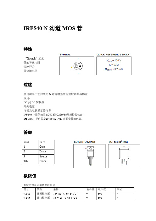
IRF540 N沟道MOS管特性
‘Thrench’工艺
低的导通内阻
快速开关
低热敏电阻
综述
使用沟渠工艺封装的N通道增强型场效应功率晶体管应用:
DC到DC转换器
开关电源
电视及电脑显示器电源
IRF540中提供的是SOT78(TO220AB)常规铅的包裹。
IRF540S中提供的是SOT404(D PAK)表面安装的包裹。
管脚
极限值
雪崩能量极限值
热敏电阻
电特性
反向二极管极限值及特性
底座温度-自然功率降低百分比
图1:自然功率损耗
底座温度-漏电流降低百分比
图2 :自然持续漏电流
漏源极电压-脉冲漏极电流峰值
图3 :安全操作区域
脉宽-瞬态热阻抗
图4:瞬态热阻抗
漏源极电压-漏极电流
图5:典型输出特性
漏极电流-漏源极导通阻抗
图6:典型导通阻抗
图7:典型传递特性
图8:典型跨导
图9:漏源极导通阻抗
图10:门阀电压
图11:阈漏极电流
图12:典型电容值
图13:典型的反向二极管电流
图14:最大允许非重复性雪崩电流(IAS)和雪崩的时间。
irf540场效应管参数
irf540场效应管参数IRF540场效应管参数一、IRF540场效应管简介IRF540是一种N沟道MOSFET,是国际上常用的高功率场效应管之一。
它具有低开启电压、高控制灵敏度和大电流能力等特点,广泛应用于各种开关电源、逆变器、电机驱动器等高频高压开关电路中。
二、IRF540场效应管参数1. 最大耗散功率(Pd):150W最大耗散功率是指场效应管在正常工作状态下能够承受的最大功率。
超过这个值会导致场效应管过热甚至烧毁。
2. 最大漏极-源极电压(Vds):100V最大漏极-源极电压是指场效应管在正常工作状态下能够承受的最大电压。
超过这个值会导致场效应管击穿损坏。
3. 最大漏极电流(Id):33A最大漏极电流是指场效应管在正常工作状态下能够承受的最大电流。
超过这个值会导致场效应管过载损坏。
4. 静态漏极-源极电阻(Rds(on)):0.077Ω静态漏极-源极电阻是指场效应管在正常工作状态下漏极-源极间的电阻值。
该值越小,表示场效应管的导通能力越强。
5. 门极-源极开启电压(Vgs(th)):4V ~ 5V门极-源极开启电压是指场效应管开始导通的门极-源极电压。
该值越小,表示场效应管的控制灵敏度越高。
6. 门极最大电压(Vgs(max)):20V门极最大电压是指场效应管能够承受的最大门极-源极电压。
超过这个值会导致场效应管损坏。
三、IRF540场效应管特性曲线IRF540场效应管特性曲线反映了其在不同工作条件下的漏电流与漏极-源极电压之间的关系。
通过分析特性曲线可以得到IRF540的一些重要参数,如开启电压、截止电流等。
四、IRF540场效应管使用注意事项1. 在使用前必须仔细阅读数据手册,并按照手册规定进行正确连接和使用。
2. 需要注意场效应管的静态电压和电流,避免超过最大值。
3. 在使用场效应管时需要注意散热,以免过热损坏。
4. 在选择场效应管时需要根据实际需求选择合适的型号和参数,以免出现过载或不足的情况。
irf540参数

IRF540参数简介IRF540是一种高功率N沟道MOSFET(金属氧化物半导体场效应晶体管)。
它具有低开启电阻和高电流能力,适用于各种高电压和高功率应用,如电源开关、电机驱动器和电子开关等。
参数概述IRF540的参数可以分为静态参数和动态参数两部分:静态参数静态参数是指在稳态工作条件下的性能指标,包括: - 额定电压:VDS(Drain-Source Voltage)表示MOSFET的最大允许电压,通常为100V。
- 额定电流:ID (Drain Current)表示经过MOSFET的最大允许电流,它受到功率和散热的限制,通常为28A。
- 导通电阻:RDS(ON)(Drain-Source On-Resistance)表示MOSFET在导通状态下的电阻,一般为0.077Ω。
- 阈值电压:VGS(TH)(Gate-Source Threshold Voltage)表示MOSFET的门极阈值电压,它决定了其导通状态,通常为2-4V。
- 级间电容:Ciss(Input Capacitance)表示MOSFET的输入电容,一般为1100pF。
- 级间电容:Crss(Reverse Transfer Capacitance)表示MOSFET的反向传输电容,一般为5pF。
- 输出电容:Coss(Output Capacitance)表示MOSFET的输出电容,一般为400pF。
动态参数动态参数是指在快速开关过程中的性能指标,包括: - 上升时间:tr(Turn-On Time)表示MOSFET从导通到截止的时间,当输入信号施加到开关管时,tr是S型曲线上的一点。
- 下降时间:tf(Turn-Off Time)表示MOSFET从截止到导通的时间。
主要应用IRF540由于其高功率和高电流能力,在各个领域中得到了广泛的应用,包括但不限于以下几个方面:电源开关IRF540可以作为电源开关使用,用于调节和分配电源。
- 1、下载文档前请自行甄别文档内容的完整性,平台不提供额外的编辑、内容补充、找答案等附加服务。
- 2、"仅部分预览"的文档,不可在线预览部分如存在完整性等问题,可反馈申请退款(可完整预览的文档不适用该条件!)。
- 3、如文档侵犯您的权益,请联系客服反馈,我们会尽快为您处理(人工客服工作时间:9:00-18:30)。
Power MOSFETIRL540, SiHL540Vishay SiliconixFEATURES•Dynamic dV/dt Rating•Repetitive Avalanche Rated •Logic-Level Gate Drive•R DS(on) Specified at V GS = 4 V and 5 V •175 °C Operating Temperature •Fast Switching •Ease of Paralleling •Lead (Pb)-free AvailableDESCRIPTIONThird generation Power MOSFETs from Vishay provide the designer with the best combination of fast switching,ruggedized device design, low on-resistance and cost-effectiveness.The TO-220 package is universally preferred for all commercial-industrial applications at power dissipation levels to approximately 50 W. The low thermal resistance and low package cost of the TO-220 contribute to its wide acceptance throughout the industry.Notesa.Repetitive rating; pulse width limited by maximum junction temperature (see fig. 11).b.V DD = 25 V, starting T J = 25 °C, L = 841 µH, R G = 25 Ω, I AS = 28 A (see fig. 12c).c.I SD ≤ 28 A, dI/dt ≤ 170 A/µs, V DD ≤ V DS , T J ≤ 175 °C.d. 1.6 mm from case.PRODUCT SUMMARYV DS (V)100R DS(on) (Ω)V GS = 5.0 V0.077Q g (Max.) (nC)64Q gs (nC)9.4Q gd (nC)27ConfigurationSingleTO-220GDSORDERING INFORMATIONPackage TO-220Lead (Pb)-free IRL540PbF SiHL540-E3SnPbIRL540SiHL540ABSOLUTE MAXIMUM RATINGS T C = 25 °C, unless otherwise notedARAMETER SYMBOL LIMITUNITDrain-Source Voltage V DS100VGate-Source Voltage V GS ± 10Continuous Drain CurrentV GS at 5.0 VT C = 25 °C I D28A T C = 100 °C20Pulsed Drain Current a I DM 110Linear Derating Factor1.0W/°CSingle Pulse Avalanche Energy b E AS 440mJ Avalanche Current aI AR 28 A Repetitive Avalanche Energy a E AR 15mJ Maximum Power Dissipation T C = 25 °CP D 150W Peak Diode Recovery dV/dt cdV/dt 5.5V/ns Operating Junction and Storage Temperature Range T J , T stg - 55 to + 175°CSoldering Recommendations (Peak Temperature)for 10 s 300d Mounting Torque6-32 or M3 screw10 lbf · in 1.1N · m* Pb containing terminations are not RoHS compliant, exemptions may apply元器件交易网IRL540, SiHL540Vishay SiliconixNotesa.Repetitive rating; pulse width limited by maximum junction temperature (see fig. 11).b.Pulse width ≤ 300 µs; duty cycle ≤ 2 %.THERMAL RESISTANCE RATINGSARAMETER SYMBOL TY.MAX.UNIT Maximum Junction-to-Ambient R thJA -62°C/WCase-to-Sink, Flat, Greasd Surface R thCS 0.50-Maximum Junction-to-Case (Drain)R thJC-1.0元器件交易网IRL540, SiHL540Vishay Siliconix TYPICAL CHARACTERISTICSFig. 1 - Typical Output Characteristics, TC = 25 °CFig. 4 - Normalized On-Resistance vs. Temperature 元器件交易网IRL540, SiHL540Vishay SiliconixFig. 5 - Typical Capacitance vs. Drain-to-Source Voltage Fig. 6 - Typical Gate Charge vs. Gate-to-Source VoltageFig. 7 - Typical Source-Drain Diode Forward Voltage元器件交易网IRL540, SiHL540 Vishay SiliconixFig. 9 - Maximum Safe Operating Area Fig. 10a - Switching Time Test Circuit Fig. 10b - Switching Time WaveformsFig. 11 - Maximum Effective Transient Thermal Impedance, Junction-to-CaseFig. 12a - Unclamped Inductive Test Circuit Fig. 12b - Unclamped Inductive Waveforms元器件交易网IRL540, SiHL540Vishay SiliconixFig. 12c - Maximum Avalanche Energy vs. Drain CurrentFig. 13a - Basic Gate Charge WaveformFig. 13b - Gate Charge Test Circuit元器件交易网IRL540, SiHL540Vishay SiliconixFig. 14 - For N-ChannelVishay Siliconix maintains worldwide manufacturing capability. Products may be manufactured at one of several qualified locations. Reliability data for Silicon Technology and Package Reliability represent a composite of all qualified locations. For related documents such as package/tape drawings, part marking, and reliability data, see /ppg?91300.元器件交易网Disclaimer Legal Disclaimer NoticeVishayAll product specifications and data are subject to change without notice.Vishay Intertechnology, Inc., its affiliates, agents, and employees, and all persons acting on its or their behalf (collectively, “Vishay”), disclaim any and all liability for any errors, inaccuracies or incompleteness contained herein or in any other disclosure relating to any product.Vishay disclaims any and all liability arising out of the use or application of any product described herein or of any information provided herein to the maximum extent permitted by law. The product specifications do not expand or otherwise modify Vishay’s terms and conditions of purchase, including but not limited to the warranty expressed therein, which apply to these products.No license, express or implied, by estoppel or otherwise, to any intellectual property rights is granted by this document or by any conduct of Vishay.The products shown herein are not designed for use in medical, life-saving, or life-sustaining applications unless otherwise expressly indicated. Customers using or selling Vishay products not expressly indicated for use in such applications do so entirely at their own risk and agree to fully indemnify Vishay for any damages arising or resulting from such use or sale. Please contact authorized Vishay personnel to obtain written terms and conditions regarding products designed for such applications.Product names and markings noted herein may be trademarks of their respective owners.元器件交易网。
