基于AD783的采样保持电路
2007年全国大学生电子设计竞赛一等奖作品——数字示波器
2007年全国大学生电子设计竞赛一等奖作品——数字示波器发布时间: 2007-11-27 20:28:37作者:责任编辑:数字示波器作者:黄霖宇、陈鹍、侯碧波一等奖作品摘要本数字示波器以单片机和FPGA为核心,对采样方式的选择和等效采样技术的实现进行了重点设计,使作品不仅具有实时采样方式,而且采用随机等效采样技术实现了利用实时采样速率为1MHz的ADC进行最大200MHz的等效采样。
同时系统还具有可测2mV小信号、波形存储回放、测频、触发沿选择、校准信号输出等功能。
AbstractThis digital oscilloscope takes a MCU and FPGA as the core .We made emphases on the choice of the sampling methods and the implement of equivalent sampling, as a result, our design not only has the real-time sampling mode but also can reach the highest equivalent sample rate of 200 MHz using the real-time sample rate of 1 MHz, by way of random equivalent sampling. At the same time, this system has many other functions, such as 2mV small-signal measuring, storage andre-display of waveform, measuring frequency, selective trigger edge , output of thecorrection signal and so on.一、总体方案设计1.方案比较与选择仔细分析题目要求,以实时采样速率为1MHz的ADC实现最大200MHz的等效采样,是本题的最大难点,也是设计的重点之一。
基于ad采样的激光稳频自动控制电路的设计
基于ad采样的激光激光稳频激光稳频自动控制电路的设计摘要本文在分析现有电路测试理论和技术的基础上根据测试要求,基于硬件电路的自动测试系统由三层结构框架组成,采用工业模拟输入输出卡本文详细介绍了控制卡实现控制通道功能的软硬件配置,同时对系统中的一些关键问题进行了理论分析和讨论,并给出了主要研究了测试生成理论,根据实际需要,给出了一种有效的多值逻辑电路测试生成算法,并从理论上分析了通道电压测量误差产生的原因。
针对不同精度的要求,提出了在有限硬件资源条件下,减小误差的两种有效方法,利用外部电路编程方法,实现了低成本的ar通道激励信号。
关键词:电路测试故障诊断测试生成敏化算法目录一、绪论 (5)(一)、实验目的 (5)1.1熟悉常见的电子元器件,了解合理布局电路的重要性; (5)1.2培训和加强电路焊接技能和故障判断及排除的动手能力; (5)1.3原电路可进行优化和扩充 (5)(二)、实验器材 (5)(三)、实验原理 (5)(四)、激光稳频方法综述 (6)二、激光稳频激光稳频自动控制的需求分析及技术简析 (7)(一)、激光稳频单元技术之一。
(7)(二)、影响激光稳频频率稳定的因素 (7)2.1温度影响 (7)2.2温度影响 (7)2.3 磁场的影响 (7)(三)、常见激光稳频方法 (8)3.1保和吸收激光稳频法分子饱和吸收法 (8)3.2 塞曼效应激光稳频原理 (8)3.3热激光稳频法 (8)3.4电阻丝加热激光稳频方法 (8)3.5频率的稳定性和复现性 (9)(四)、控制电路可逆调速的原理 (9)5.1拍频的原理 (9)三、控制电路各主要部分的介绍 (10)(一)、自动振荡器 (10)(二)、声控振荡器 (11)(三)、控制电路反转电路: (11)(四)、分压电路 (12)(五)、测试板电源系统 (13)5.1测试信号系统 (13)5.2、特殊信号通道 (13)5.3接口控制系统 (13)5.4测试信号的选通 (13)5.5信号检测系统 (14)四、实验内容 (14)(一)、设计方案及布局 (14)(二)、焊接电路 (15)五、调试并排障 (15)(一)、电路调试 (15)(二)、电路排障 (15)(二)、静态故障静态 (15)(四)、动态故障 (16)六、实验结果及心得拓展 (16)(一)、实验结果 (16)(二)、实验心得 (17)(二)、实验拓展 (17)总结 (17)七、M AT LAB仿真研究 (17)(一)、研究方法的选择 (18)(二)、仿真模型 (18)(三)、仿真实例及结果分析 (18)(四)、应用BPA 对仿真结果验证 (19)4.1BPA 仿真步骤 (19)4.2运行结果 (19)4.3参与选取 (19)结束语 (20)参考文献 (20)一、绪论脉冲染料激光器具有稳定的温度、压力、振动和波长调谐特性,常用于长时间荧光高钠层的检测。
AD783应用笔记

如何通过前端将PC声卡变成高速采样示波器作者:Doug Mercer有多种软件包可以使个人计算机(PC)中的立体声声卡提供类似示波器的显示,但低采样速率、高分辨率模数转换器(ADC)和交流耦合前端最适合20 kHz及以下的可用带宽。
现在,这种有限的带宽可以扩展——针对重复波形,可以在声卡输入前使用一个采样前端。
利用高速采样保持器(SHA)对输入波形进行二次采样,然后通过低通滤波器重建波形,并使其平滑,可以有效延展时间轴,使PC能够用作高速采样示波器。
本文描述一种能够实现这种改造的前端和探头。
图1所示为一个插入式附件的原理图,它可以配合典型PC声卡采样使用。
每个示波器通道使用一个高速采样保持放大器AD783。
SHA的采样信号由时钟分频器电路的数字输出提供,下文将通过一个例子说明。
AD783输入由一个FET缓冲,因此可以使用简单的交流/直流输入耦合。
在所示的两个通道中,当直流耦合跳线开路且输入为交流耦合时,1 MΩ电阻(R1和R3)提供直流偏置。
采样输出由图中所示的双极点有源RC网络低通滤波。
该滤波器不必是一个有源电路,但所示的滤波器能够提供有益的缓冲低阻抗来驱动PC声卡输入。
图1. 双通道模拟采样电路AD783 SHA提供高达数MHz的可用大信号带宽。
输入端的有效压摆率约为100 V/µs以上。
采用±5 V电源时,输入/输出摆幅至少为±3 V。
对于500 mV p-p以下的摆幅,小信号3 dB带宽接近50 MHz。
利用图1所示的前端电路以及采用Visual Analyser1软件的PC 声卡,可以得到一个以1 MHz频率重复的2 MHz单周期正弦波,如图2的屏幕截图所示。
采样时钟以80.321 kHz的采样速率提供250 ns宽的采样脉冲。
这里的有效水平时基为333 ns/分频比。
例子中使用的PC声卡采用SoundMax®编解码器,其采样速率为96 kSPS。
基亏A/D转换器ADS7813的信号采集系统设计

A / D , 内部 时钟 电路 , 内部基 准产 生 电路 入 。 由于从 开始 启动 到 丽 上升 后 的时 间 本 系 统 的A / D 芯 片 可 以处 理 0 ~l 0 V : 内, 转 换器 对 外 部干 扰 会 很 敏 感 …,强 的 电压 信 号 , R 和 串行 数 据 接 口 电路 等 , 同 时 ,该 A / 9 转 t 1 接 班B U F ,R 2 接G N D , 换器 可 以配 置 为 多种 输入 电压 范 围,包 括 烈推 荐 从瓦 丽 使用 1 0 0 n s 的脉冲 进 行 启动 3 Ⅲ 接 。A D S 7 8 1 3 的R E F 输 出2 . 5 V 内部 ±I O V , ±5 V,O V ~1 0 V ,0 . 5 V ~4 . 5 V 。灵 转换 。 图1 所示 为 基本 的转 换时 间 。 参 考 电压 或 者 作 为 外 部 输 入 参 考 。 同 时 活 的兼容 性 Q S P I 串行 通信 可 以通 过 内部 或 2 . 2 . 2 读 取转换 结 果 R E F 引脚 需 要 接一 个 l u F  ̄2 . 2 u F 的钽 电容 者外 部 时钟 将 数据 同步输 出。 具体 归纳 起 对 于 使用 外 部 时钟 的转 换 电路 来 说 , 到 模 拟 地 上 , 并 且 该 电 容 应 该 尽 可 能 地 来A D S 7 8 1 3 具 有 如 下特 性 : ( 1 ) 最 大转 换 第 n 次 的转 换 结 果 可 以在 本 次 转换 完 成 后 靠 近A D S 7 8 1 3 芯 片 。C A P 脚 用 来 补 偿 内部 时间2 0 u s ;( 2 ) 单 电源+ 5 V 供 电; ( 3 ) 引脚 与 到 下一 次转 换 开始 前 这 段时 间输 出, 也可 相 关脉 冲 ,需 要 接 一个 l u F 钽 电容 和 一个 1 2 位 的A D S 7 8 1 2 完 全 兼容 ; ( 4 ) 易于 使用 的 以在第 n + 1 次 转 换 过 程 中输 出 , 或者 是 在 0 . 0 1 u F 的 陶 瓷 电容到模 拟 地 ,钽 电容 和 陶 串行数 据接 口; ( 5 ) 最 大积分 和微 分非 线性 本 次转 换完 成 后和 下 一 次转 换过 程 中段 续 瓷 电容 并联 相接 ,且 陶 电容应 当尽 量 靠近 输 出。 A D S 7 8 1 3 芯 片 。 电容总 量对 于A D S 7 8 1 3 的工 对 于 一 般 应 用 场 合 , 每 个 输 出 位 在 作 至 关重 要 , 该 电容 大 于 2 . 0 u F 将超 出其 D A T A C L K 的下 降沿 都是 无 效 的 ,但 某 些 情 缓冲 能力 ,小 于 0 . 5 u F 可 能会 提 供 不 了足 况 下 ,输 出位 在 D A T A C L K 的 上 升沿 是有 效 够 的补 偿 ,影 响其 输 出正 确 的数字 量 。本 的 ,但 是 需要 加 一个 额 外 的时钟 周 期为 最 系统 在 设计 电路 板 时将 数 字 电路 的地 和模 后 一位 服 务 。且 这个 额 外 的D A T A C L K 信 号 拟 电路 的地 用光 耦 隔离 ,电源 用专 用 的 电 必须 为低 电平 或 者西 必须 在 丽 上 升 前为 源 隔离 芯片 ,从 而 防止 单 片机 及其 他 高速 高 电平 。 数 字 电路 对 模 拟 地 产 生 影 响 , 进 而 影 响 如 果 该 时间 内该条 件未 能得 到 遵 守 , A 9 S 7 8 1 3 的 处 理结 果 。在采 用 恒 压源 加 载 A D S 7 8 1 3 的移 位 寄存 器 将 不 会 被转 换 结 果 在 多路 选 择 器 上 的条 件 下 ,A D S 7 8 1 3 的实 更新 ,前一 个 移位 寄 存器 的 内容 将 保持 不 测精度 可 以达到 l 5 位。 变 ,转换 的新 结果 将丢 失 。 系 统 的核 心 处 理 器采 用 8 位 高速 单 片 串行 传 送 转 换 结果 由D A T A C L K 的上 升 机P I C 1 6 F 8 7 7 A , 由于 A D S 7 8 l 3 的 串行通 信 沿 触 发 。数 据 以 l 6 位 , 二进 制 的补 码 的格 Q S P I 是 一种 兼 容性 的 串行通 信 ,所 以不能 式输 出 。 直接 与 单 片 机 的S P I 串 口进 行通 信 ,本 系
全国电子竞赛放大器类赛题
“放大器类”赛题2.1.1 “放大器类赛题” 历届都有在9届电子设计竞赛中,“放大器类赛题” 除了1994年外,其它每届都有,共有9题:①实用低频功率放大器(1995年A题);②测量放大器(1999年A题);③高效率音频功率放大器(2001年D题);④宽带放大器(2003年B题);⑤程控滤波器(2007年D 题本科组);⑥可控放大器(2007年I题高职高专组);⑦宽带直流放大器(2009年C题);⑧数字幅频均衡的功率放大器(2009年F题);⑨低频功率放大器(2009年G题)。
其中:与音频功率放大器有关的有4题。
与宽带放大器有关的有2题。
与直流、低频放大器有关的有3题。
比较历届赛题可以看到,“放大器类”赛题的要求是越来越高,如:在“程控滤波器(2007年D题本科组)”中要求放大器电压增益为60dB,输入信号电压振幅为10mV。
制作“简易幅频特性测试仪”,其扫频输出信号的频率变化范围是100Hz~200kHz,频率步进10kHz。
在“数字幅频均衡的功率放大器(2009年F题)” 中要求:当输入正弦信号v i电压有效值为5mV、功率放大器接8Ω电阻负载(一端接地)时,要求输出功率≥10W。
功率放大电路的-3dB通频带为20Hz~20kHz。
功率放大电路的效率≥60%。
宽带放大器(2003年B题)”中要求3dB通频带10kHz~6MHz,最大增益≥58dB(3dB 通频带10kHz~6MHz,最大输出电压有效值≥6V,数字显示输出正弦电压有效值。
“宽带直流放大器(2009年C题)”中要求最大电压增益A V≥60dB,输入电压有效值V i≤10 mV。
放大器的输入电阻≥50Ω,3dB通频带0~10MHz;负载电阻(50±2)Ω,最大输出电压正弦波有效值V o≥10V。
注意:放大器同时也是各赛题中一个必不可少的组成部分。
2.1.2 常用的一些放大器(包含OP)芯片历届的“放大器类赛题” (包括其他赛题)中使用到的一些放大器(包含OP)芯片有:AD526精确程控放大器ADI公司,AD603,低噪声、90 MHz可变增益放大器.,ADI公司,AD605双通道、低噪声、单电源可变增益放大器,ADI公司,AD620低漂移、低功耗仪表放大器,增益设置范围1~10000 ADI公司, AD783,采样保持电路,ADI公司,AD811高性能视频运算放大器(电流反馈型宽带运放),ADI公司,AD818高速低噪声电压反馈型运放,ADI公司,AD8011 300 MHz、1 mA 电流反馈放大器,ADI公司,AD8056双路、低成本、300 MHz电压反馈型放大器ADI公司,AD8564,四路7 ns单电源高速比较器,ADI公司,AC524/AC525 5~500 MHz级联放大器,teledyne 公司,BUF634,250mA高速缓冲器,TI公司,/cnCA3140单运算直流放大器,Intersil Corporation,HFA1100 850MHz、低失真电流反馈放大器,Intersil Corporation,INA118精密低功耗仪表放大器,TI公司,/cnLF356 JFET输入运算放大器,National Semiconductor Corpora,LM311具有选通信号的差动比较器,National Semiconductor Corpora,LF356,JFET输入运算放大器,National Semiconductor Corpora,LM393电压比较器,National Semiconductor Corpora,LM7171高速电压反馈运算放大器,National Semiconductor Corpora,LM358/LM158/LM258/LM2904双运算放大器,National Semiconductor Corpora,LM2902,LM324/LM324A,LM224/ LM224A四运算放大器,National Semiconductor Corpora,LT1210 1.1A,35MHz电流反馈放大器,linear公司,/product/LT1210 MAX4256,UCSP封装、单电源、低噪声、低失真、满摆幅运算放大器,Maxim公司,MAX912, MAX913单/双路、超高速、低功耗、精密的TTL比较器,Maxim公司,MAX477 ,300MHz、高速运算放大器,Maxim公司,MAX427/ MAX437低噪声、高精度运算放大器,Maxim公司MAX900高速、低功耗、电压比较器,Maxim公司NE5532双路低噪声高速音频运算放大器,TI公司,/cnNE5534低噪声高速音频运算放大器,TI公司,/cnOP27低噪声、精密运算放大器ADI公司,OP37低噪声、精密运算放大器ADI公司,OPA637,精密、高速、低漂移、高增益放大器,TI公司,/cnOPA637,精密、高速、低漂移高增益放大器,TI公司,/cnOPA642高速低噪声电压反馈型运放,TI公司,/cnOPA690,宽带50MHz、电压反馈运算放大器,TI公司,/cnOPA690 高速、电压反馈型运放(大于等于50MHz),TI公司,/cn PGA202KP,数字可编程仪表放大器,TI公司,/cnTHS3091单路高压低失真电流反馈运算放大器,TI公司,/cnTHS3092高压低失真电流反馈运算放大器,TI公司,/cnTL084,JFET 输入运算放大器,TI公司,/cnµA741标准线性放大器,TI公司,/cn以上各放大器IC和OP的更多资料,可以登录有关网站查询得到(以运算放大器的型号为关键词)。
多功能计量芯片ADE7878在变电站测控装置中的应用
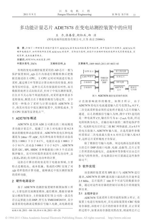
Q/Var -650.5 -648.4 -648.8 0.499 0.503 0.503
站已投运数百台 ,2 年多的实际运行表明 , 该装置能 满足变电站对电力系统运行监测的技术要求 , 相对 于传统测控采样方式 , 精度更加高 , 运行更加稳定 。
Applications of Multifunctional Measurement IC ADE7878 in Substation Measurement and Control Equipment
WANG Li, ZHANG Chun-lei, HU Hong-bing, ZHENG Jie (NARI Technology Development Co. Ltd., Nanjing 210061, China) Abstract : The paper introduces the applications of a new multifunctional measurement IC ADE7878 in substation measurement and control equipment, including chip features, ADE878 hardware circuit design and how to use the software to achieve ADE7878 sampling. Experimental results show that this design approach has higher precision, simpler, lower cost and so on compared with traditional sampling methods. Key words : ADE7878; measurement and control equipment; SPI
采样保持器 AD783应用电路

AD783的电路1、AD783高速采样保持放大器简介AD783是高速单片采样保持放大器(SHA),提供典型250ns采样时间达到0.01%,在最高输入频率100kHz时规定和测试保持模式总谐波失真。
AD783的基本特点与AD781相同。
AD783采用模拟器件公司的ABCMOS制造工艺,ABCMOS工艺综合了高性能、低噪声双极性电路和低功率CMOS逻辑,提供一个精确、高速和低功率的SHA。
AD783有J级、A级、S级3个温度等级,其引脚排列如图所示。
2、采样保持放大器AD783与AD670的接口电路如图所示为由AD783与低成本信号调节8位A/D转换器AD670构成的接口电路。
由于AD783具有15MHz小信号带宽,因此可以将其用于低于这个频率的信号采集的应用场合。
该电路输入信号为载波10.7MHz中频信号(IF),中频信号采用移频键控调制方式(FSK),调制信号频率为5kHz。
“时钟输入”直接接到AD783的S/H脚,向采样保持放大器发出采样或保持命令,AD783输出保持信号,送到8位A/D转换器AD670,由AD670将模拟信号转换为8位数字信号输出。
“时钟输入”经过单稳(ONE-SHOT)延迟10μs后加到AD670的R/W端(21脚),延迟的目的在于适应AD783保持模式150ns的建立时间,因此整个系统的传输时间为10.15μs。
输入信号为载波10.7MHz中频信号(IF)的全幅度范围为255mV,在此基础上变换器AD670有全8位的动态范围。
AD670的最大采样率为10μs,因此符合最大信号带宽50kHz的要求。
3、采样保持放大器AD783与AD671的接口电路4、数据采集系统基本接地和耦合电路(采样保持放大器AD783)如图所示为数据采集系统基本接地和耦合电路。
作为任何一个高速、高分辨率数据采集系统,电源都必须很好地调节,对额外的高频噪声(纹波)必须予以抑制。
图中AD783电源连接可以很好地实现上述要求,同时有能力传输瞬间电流给器件。
基于ADS7834和ARM实用信号采集系统的设计
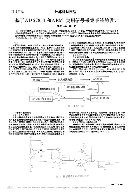
3. 2. 1. 1 SP I 工作模式选择
根据以上表明: A D 转换是在第二个时钟周期的下降沿开 始输出第一位 ( 最高位) 数据, 而 SP I 的工作模式 B 也是在时钟 的下降沿开始输出数据, 所以选择工作模式 B。 3. 2. 1. 2 转换控制问题 由于 AD S7834 是 12 位 A D 转换器, 每次转换后结果位 12 位数据, 而 SP I 的接收寄存器则为 8 位, 每次只能接收 8 位数 据, 所以无法一次接收 12 位的数据, 所以一般的设计都会根据 A D 转换器的要求, 选择相应位数更多 ( 如 16 位) 的处理器, 这 样相对而言就增加了设计成本。 或者根据处理器的要求, 选择位 数较少的 A D 转换器 ( 如 8 位) , 这样又降低了采集的精度, 影 响了性能。 其实根据 A D 转换和 SP I 的工作时序特点可利用巧 妙的编程实现采用 8 位接收寄存器接收 12 位数据, 并且及时存 储。 采用如图 7 控制模式就可实现以上功能, 因为 SP I 的读写是 同时进行的, 所以可以利用 SP I 的写功能来控制 SP I 的接收, 而 利用 GP I O 来控制 CONV 的信号, SP I 读写两次为 CONV 信号 的一个周期。
口 [2 ] , 既可以作为主 SP I 使用, 也可以作为从 SP I 使用。 主要特 点: 与 SP I 协议 ( ver. 2. 11) 兼容、 8 位发送移位寄存器、 8 位接 收移位寄存器、 8 位预分频器。 2. 4. 2 SP I 结构和工作原理 发送移位寄存器、 接 SP I 模块由 4 部分构成: 时钟分频器、 收移位寄存器、 控制逻辑等。 其结构如图 5 所示。
来消除干扰, 从而提高了选择性。 本文采用了光电比色法, 即将 液体放置在安装了发光二级管和光电接收管的容器中, 不同浓 度的液体吸光度不同, 通过光电转换产生的电压不同来测量液 体浓度, 原理见图 2 的前面部分电路。 2. 2. 2 信号放大和滤波电路 光电比色法产生的一般为毫伏级微电压信号, 需要经过放 大和滤波去除干扰并转换为适合 A D 转换的信号。 系统设计的 放大电路如图 2 所示, 主要采用高精度放大集成芯片 O P27, 整 个电路放大倍数为 1000、 通频带为 0 ~ 500H z。
采样保持电路图(五款采样保持电路设计原理图详解)

采样保持电路图(五款采样保持电路设计原理图详解)采样保持电路(采样/保持器)又称为采样保持放大器。
当对模拟信号进行A/D转换时,需要一定的转换时间,在这个转换时间内,模拟信号要保持基本不变,这样才能保证转换精度。
采样保持电路即为实现这种功能的电路。
采样保持电路能够跟踪或者保持输入模拟信号的电平值。
在理想状况下,当处于采样状态时,采样保持电路的输出信号跟随输入信号变化而变化;当处于保持状态时,采样保持电路的输出信号保持为接到保持命令的瞬间的输入信号电平值。
当电路处于采样状态时开关导通,这时电容充电,如果电容值很小,电容可以在很短的时间内完成充放电,这时,输出端输出信号跟随输入信号的变化而变化;当电路处于保持状态时开关断开,这是由于开关断开,以及集成运放的输入端呈高阻状态,电容放电缓慢,由于电容一端接由集成运放构成的信号跟随电路,所以输出信号基本保持为断开瞬间的信号电平值。
采样保持电路图设计(一)采样保持放大器SMP04用做多路输出选择器电路图如图所示为SMP04用做多路输出选择器,与解码器、D/A转换器构成的四路数字-模拟转换电路。
数字信号输入模数转换器DAC8228,输出产生5~10V模拟电压送副SMP04,地址输入通道解码器,不同的地址解码后分别控制四路开关,以分别输出四模拟信号。
采用DAC8228产生DAC电压输出可以使电路得以最大的简化。
为了将输出电压干扰减小到最小,在采样信号被确认之前,必须保证有5μs的最后电压建立时间。
每一个采样保持放大器必须在每一秒钟或更低时问刷新一次,以确保输出电压下降率不超过10mV或1/2LSB(最小有效位)。
采样保持电路图设计(二)如图所示为由SMP04与运放构成的增益为10的采样保持放大电路。
电路中将SMP04置于运放OP490的反馈回路中,当S非/H=0时,SMP04内部开关闭合,运放OP490的反馈回路接通,电路增益由运放本身及反馈电阻决定,图中增益设置为10,输出端输出放大后的采样电压。
基于AD783的采样保持电路
1293.6.1 基于AD783的采样/保持电路1. AD783的主要技术性能与特点AD783是ADI 公司生产的一个高速的、单片采样/保持放大器电路,采样时间为250ns (0.01%),保持值下降速率为0.02mV/ms ,典型谐波失真为–85dB ,不需要连接外部元件,电源电压±5V ,功率消耗为95mW ,温度范围为–40℃~+85℃。
2. AD783的引脚功能和封装形式AD783采用SOIC-8封装,引脚端1(V CC )和5(V EE )为电源电压正端和负端,引脚端2(IN )和8(OUT )为输入端和输出端,引脚端3(COMMON )为公共地。
3. AD783的应用电路(1)电源和接地连接方式AD783可直接与AD671、AD7586、AD674B 、AD774B 、AD7572 和AD7672等高速ADC 连接使用,推荐的电源和接地连接方式如图3.6.1所示。
图3.6. 1 电源和接地连接方式(2)与ADC 的连接电路例AD783与AD670的连接电路如图3.6.2所示,AD783与AD671的连接电路如图3.6.3所示。
图3.6.2 AD783与AD670的连接电路130图3.6.3 AD783与AD671的连接电路3.6.2基于SHC5320的采样/保持电路1. SHC5320的主要技术性能与特点SHC5320是TI 公司生产的(原BURR-BROWN 公司)是双极性单片采样/保持器电路,模拟输入范围为-10V ~+10V ,共模电压范围为-10V ~+10V ,输入阻抗大于1M Ω,失调电流小于±300nA ,输出电压范围为-10V ~+10V ,输出电流大于±10mA ,输出阻抗小于1Ω,输入漂移小于±20μV /℃,共模抑制比大于72dB ,电源抑制比大于65dB ,压摆率典型值为45V /μs ,采样时间小于1.5μs ,从采样到保持的切换时间为165~350ns ,下降速率典型值为0.5μV /μs (在25℃时),差分输入,控制接口与TTL 逻辑电平兼容,工作电源电压±12V ~±18V ,电流消耗±13mA ,工作温度范围-40℃~+80℃,可广泛地应用于高精度数据采集系统、自动调零电路和D/A 转换等电路中。
AD783资料
FUNCTIONAL BLOCK DIAGRAMV CC INCOMMONNCOUT S/H NC V EENC = NO CONNECTREV.AInformation furnished by Analog Devices is believed to be accurate and reliable. However, no responsibility is assumed by Analog Devices for its use, nor for any infringements of patents or other rights of third parties which may result from its use. No license is granted by implication or otherwise under any patent or patent rights of Analog Devices.aComplete Very High Speed Sample-and-Hold AmplifierAD783*One Technology Way, P.O. Box 9106, Norwood, MA 02062-9106, U.S.A.Tel: 617/329-4700Fax: 617/326-8703FEATURESAcquisition Time to 0.01%: 250 ns Typical Low Power Dissipation: 95 mW Low Droop Rate: 0.02 V/sFully Specified and Tested Hold Mode Distortion Total Harmonic Distortion: –85 dB Aperture Jitter: 50 ps Maximum Internal Hold CapacitorSelf-Correcting Architecture8-Pin Mini Cerdip and SOIC PackagesPRODUCT DESCRIPTION The AD783 is a high speed, monolithic sample-and-hold amplifier (SHA). The AD783 offers a typical acquisition time of 250 ns to 0.01%. The AD783 is specified and tested for hold mode total harmonic distortion with input frequencies up to 100 kHz. The AD783 is configured as a unity gain amplifier and uses a patented self-correcting architecture that minimizes hold mode errors and ensures accuracy over temperature. The AD783 is self-contained and requires no external components or adjustments.The AD783 retains the held value with a droop rate of 0.02 µV/µs. Excellent linearity and hold mode dc and dynamic perfor-mance make the AD783 ideal for high speed 12- and 14-bit analog-to-digital converters.The AD783 is manufactured on Analog Devices’ ABCMOS process which merges high performance, low noise bipolar circuitry with low power CMOS to provide an accurate, high speed, low power SHA.The J grade device is specified for operation from 0°C to +70°C and the A grade from –40°C to +85°C. The J and A grades are available in 8-pin cerdip and SOIC packages. The militarytemperature range version is specified for operation from –55°C to +125°C and is available in an 8-pin cerdip package. For details refer to the Analog Devices Military Products Databook or AD783/883B data sheet.*Protected by U.S. Patent Number 4,962,325.PRODUCT HIGHLIGHTS1.Fast acquisition time (250 ns), low aperture jitter (20 ps) and fully specified hold mode distortion make the AD783 an ideal SHA for sampling systems.2.Low droop (0.02 µV/µs) and internally compensated hold mode error result in superior system accuracy.3.Low power (95 mW typical), complete functionality and small size make the AD783 an ideal choice for a variety of high performance applications.4.The AD783 requires no external components or adjustments.5.The AD783 is an excellent choice as a front-end SHA for high speed analog-to-digital converters such as the AD671,AD7586, AD674B, AD774B, AD7572 and AD7672.6.Fully specified and tested hold mode distortion guarantees the performance of the SHA in sampled data systems.AD783–SPECIFICATIONSDC SPECIFICATIONS(T MIN to T MAX with V CC = +5 V ؎ 5%, V EE = –5 V ؎ 5%, C L = pF, unless otherwise noted)AD783J/AParameter Min Typ Max Units SAMPLING CHARACTERISTICSAcquisition Time5 V Step to 0.01%250375ns5 V Step to 0.1%200350nsSmall Signal Bandwidth15MHzFull Power Bandwidth2MHz HOLD CHARACTERISTICSEffective Aperture Delay (+25°C)–301530ns Aperture Jitter (+25°C)2050psHold Settling (to 1 mV, +25°C)150200nsDroop Rate0.021µV/µs Feedthrough (+25°C)(V IN = ±2.5 V, 500 kHz)–80dB ACCURACY CHARACTERISTICS1Hold Mode Offset–50+5mVHold Mode Offset Drift10µV/°C Sample Mode Offset50200mV Nonlinearity±0.005% FS Gain Error±0.03±0.1% FS OUTPUT CHARACTERISTICSOutput Drive Current–5+5mA Output Resistance, DC0.30.6ΩTotal Output Noise (DC to 5 MHz)150µV rms Sampled DC Uncertainty85µV rms Hold Mode Noise (DC to 5 MHz)125µV rms Short Circuit CurrentSource20mA Sink13mA INPUT CHARACTERISTICSInput Voltage Range–2.5+2.5VBias Current100250nAInput Impedance10MΩInput Capacitance2pF DIGITAL CHARACTERISTICSInput Voltage Low0.8VInput Voltage High 2.0VInput Current High (V IN = 5 V)210µA POWER SUPPLY CHARACTERISTICSOperating Voltage Range±4.75±5±5.25VSupply Current9.517mA+PSRR (+5 V ± 5%)4565dB–PSRR (–5 V ± 5%)4565dB Power Consumption95175mW TEMPERATURE RANGESpecified Performance (J)0+70°C(A)–40+85°CNOTES1Specified and tested over an input range of ±2.5 V.Specifications subject to change without notice.–2–REV. AAD783REV. A –3–HOLD MODE AC SPECIFICATIONSAD783J/A ParameterMinTyp Max Units TOTAL HARMONIC DISTORTION f IN = 100 kHz –85–80dB f IN = 500 kHz–72dB SIGNAL-TO-NOISE AND DISTORTION f IN = 100 kHz 77dB f IN = 500 kHz70dBINTERMODULATION DISTORTION (F1 = 99 kHz, F2 = 100 kHz)Second Order Products –80dB Third Order Products–85dBNOTES 1f IN amplitude = 0 dB and f SAMPLE = 300 kHz unless otherwise indicated.Specifications subject to change without notice.(TMIN to T MAX with V CC = +5 V ؎ 5%, V EE = –5 V ؎ 5%, C L = 50 pF, unless otherwise noted)ABSOLUTE MAXIMUM RATINGS*WithSpecRespect to Min Max Units V CC COM –0.5+6.5V V EECOM –6.5+0.5V Analog Input COM –6.5+6.5V Digital InputCOM–0.5+6.5VOutput Short Circuit to Ground, V CC , or V EE Indefinite Maximum Junction Temperature +175°C Storage–65+150°C Lead Temperature (10 sec max)+300°C*Stresses above those listed under “Absolute Maximum Ratings” may cause permanent damage to the device. This is a stress rating only and functional operation of the device at these or any other conditions above those indicated in the operational section of this specification is not implied.PIN CONFIGURATIONV CC INCOMMONNCOUT NC V EES/H NC = NO CONNECTCAUTIONESD (electrostatic discharge) sensitive device. Electrostatic charges as high as 4000V readily accumulate on the human body and test equipment and can discharge without detection.Although the AD783 features proprietary ESD protection circuitry, permanent damage may occur on devices subjected to high energy electrostatic discharges. Therefore, proper ESD precautions are recommended to avoid performance degradation or loss of functionality.ORDERING GUIDETemperature Package Model1Range Description Options 2AD783JQ 0°C to +70°C 8-Pin Cerdip Q-8AD783AQ –40°C to +85°C 8-Pin Cerdip Q-8AD783JR 0°C to +70°C 8-Pin SOIC R-8AD783AR–40°C to +85°C8-Pin SOICR-8NOTES 1For details on grade and package offerings screened in accordance with MIL-STD-883, refer to the Analog Devices Military Products Databook or current AD783/883B data sheet.2Q = Cerdip, R = SOIC.AD783–Typical CharacteristicsREV. A–4–01M30101405060100k10k1k100FREQUENCY – HzP S R R – d BPower Supply Rejection Ratio vs. Frequency 200–200–100–150–2.50–5050100150+2.5INPUT VOLTAGE – VB I A SC U R R E N T –n ABias Current vs. Input Voltage10.00.0011501.00.01250.11251007550TEMPERATURE – °CD R O O P R A TE – µV /µsDroop Rate vs. Temperature, V IN = 0 V053002001250432INPUT STEP – VA C Q U I S I T I O N T I M E –n sAcquisition Time (to 0.01%) vs. Input Step SizeAD783REV. A –5–DEFINITIONS OF SPECIFICATIONSAcquisition Time —The length of time that the SHA must remain in the sample mode in order to acquire a full-scale input step to a given level of accuracy.Small Signal Bandwidth —The frequency at which the held output amplitude is 3 dB below the input amplitude, under an input condition of a 100 mV p-p sine wave.Full Power Bandwidth —The frequency at which the held output amplitude is 3 dB below the input amplitude, under an input condition of a 5 V p-p sine wave.Effective Aperture Delay —The difference between the switch delay and the analog delay of the SHA channel. A negative number indicates that the analog portion of the overall delay is greater than the switch portion. This effective delay represents the point in time, relative to the hold command, that the input signal will be sampled.Aperture Jitter —The variations in aperture delay forsuccessive samples. Aperture jitter puts an upper limit on the maximum frequency that can be accurately sampled.Hold Settling Time —The time required for the output tosettle to within a specified level of accuracy of its final held value after the hold command has been given.Droop Rate —The drift in output voltage while in the hold mode.Feedthrough —The attenuated version of a changing input signal that appears at the output when the SHA is in the hold mode.Hold Mode Offset —The difference between the input signal and the held output. This offset term applies only in the hold mode and includes the error caused by charge injection and all other internal offsets. It is specified for an input of 0 V.Sample Mode Offset —The difference between the input and output signals when the SHA is in the sample mode.Nonlinearity —The deviation from a straight line on a plot of input vs. (held) output as referenced to a straight line drawn between endpoints, over an input range of –2.5 V and +2.5 V.Gain Error —Deviation from a gain of +1 on the transfer function of input vs. held output.Power Supply Rejection Ratio —A measure of change in the held output voltage for a specified change in the positive or negative supply.Sampled DC Uncertainty —The internal rms SHA noise that is sampled onto the hold capacitor.Hold Mode Noise —The rms noise at the output of the SHA while in the hold mode, specified over a given bandwidth.Total Output Noise —The total rms noise that is seen at the output of the SHA while in the hold mode. It is the rmssummation of the sampled dc uncertainty and the hold mode noise.Output Drive Current —The maximum current the SHA can source (or sink) while maintaining a change in hold mode offset of less than 2.5 mV.Signal-To-Noise and Distortion (S/N+D) Ratio —S/N+D is the ratio of the rms value of the measured input signal to the rms sum of all other spectral components below the Nyquist frequency, including harmonics but excluding dc. The value for S/N+D is expressed in decibels.Total Harmonic Distortion (THD)—THD is the ratio of the rms sum of the first six harmonic components to the rms value of the measured input signal and is expressed in decibels.Intermodulation Distortion (IMD)—With inputs consisting of sine waves at two frequencies, fa and fb, any device withnonlinearities will create distortion products, of order (m+n), at sum and difference frequency of mfa ±nfb, where m, n = 0, 1, 2,3.... Intermodulation terms are those for which m or n is not equal to zero. For example, the second order terms are (fa+fb)and (fa–fb), and the third order terms are (2fa+fb), (2fa–fb),(fa+2fb) and (fa–2fb). The IMD products are expressed as the decibel ratio of the rms sum of the measured input signals to the rms sum of the distortion terms. The two signals are of equal amplitude, and peak value of their sums is –0.5 dB from full scale. The IMD products are normalized to a 0 dB input signal.FUNCTIONAL DESCRIPTIONThe AD783 is a complete, high speed sample-and-holdamplifier that provides high speed sampling to 12-bit accuracy in 250 ns.The AD783 is completely self-contained, including an on-chip hold capacitor, and requires no external components or adjust-ments to perform the sampling function. Both input and output are treated as a single-ended signal, referred to common.The AD783 utilizes a proprietary circuit design which includes a self-correcting architecture. This sample-and-hold circuit corrects for internal errors after the hold command has been given, by compensating for amplifier gain and offset errors, and charge injection errors. Due to the nature of the design, the SHA output in the sample mode is not intended to provide an accurate representation of the input. However, in hold mode,the internal circuitry is reconfigured to produce an accurately held version of the input signal. Below is a block diagram of the AD783.V CC INCOMMONNCOUT S/H NC V EENC = NO CONNECTFunctional Block DiagramAD783REV. A–6–DYNAMIC PERFORMANCEThe AD783 is compatible with 12-bit A-to-D converters interms of both accuracy and speed. The fast acquisition time, fast hold settling time and good output drive capability allow the AD783 to be used with high speed, high resolution A-to-D converters like the AD671 and AD7586. The AD783’s fastacquisition time provides high throughput rates for multichannel data acquisition systems. Typically, the AD783 can acquire a 5 V step in less than 250 ns. Figure 1 shows the settling accuracy as a function of acquisition time.0.080.060.040.0200ACQUISITION TIME – nsV A C Q U I S I T I O N A C C U R A C Y – %O UT Figure 1.V OUT Settling vs. Acquisition TimeThe hold settling determines the required time, after the hold command is given, for the output to settle to its final specified accuracy. The typical settling behavior of the AD783 is 150 ns.The settling time of the AD783 is sufficiently fast to allow the SHA, in most cases, to directly drive an A-to-D converter without the need for an added “start convert” delay.HOLD MODE OFFSETThe dc accuracy of the AD783 is determined primarily by the hold mode offset. The hold mode offset refers to the difference between the final held output voltage and the input signal at the time the hold command is given. The hold mode offset arises from a voltage error introduced onto the hold capacitor by charge injection of the internal switches. The nominal hold mode offset is specified for a 0 V input condition. Over the in-put range of –2.5 V to +2.5 V, the AD783 is also characterized for an effective gain error and nonlinearity of the held value, as shown in Figure 2. As indicated by the AD783 specifications,the hold mode offset is very stable over temperature.GAIN ERRORFigure 2.Hold Mode Offset, Gain Error and NonlinearityFor applications where it is important to obtain zero offset, thehold mode offset may be nulled externally at the input to the A-to-D converter. Adjustment of the offset may be accom-plished through the A-to-D itself or by an external amplifier with offset nulling capability (e.g., AD711). The offset will change less than 0.5 mV over the specified temperature range.SUPPLY DECOUPLING AND GROUNDING CONSIDERATIONSAs with any high speed, high resolution data acquisition system,the power supplies should be well regulated and free fromexcessive high frequency noise (ripple). The supply connection to the AD783 should also be capable of delivering transient currents to the device. To achieve the specified accuracy and dynamic performance, decoupling capacitors must be placed directly at both the positive and negative supply pins to com-mon. Ceramic type 0.1 µF capacitors should be connected from V CC and V EE to common.Figure 3. Basic Grounding and Decoupling DiagramAD783REV. A–7–The AD783 does not provide separate analog and digital ground leads as is the case with most A-to-D converters. The common pin is the single ground terminal for the device. It is the refer-ence point for the sampled input voltage and the held output voltage and also the digital ground return path. The common pin should be connected to the reference (analog) ground of the A-to-D converter with a separate ground lead. Since the analog and digital grounds in the AD783 are connected internally, the common pin should also be connected to the digital ground,which is usually tied to analog common at the A-to-D converter.Figure 3 illustrates the recommended decoupling and grounding practice.NOISE CHARACTERISTICSDesigners of data conversion circuits must also consider the effect of noise sources on the accuracy of the data acquisition system. A sample-and-hold amplifier that precedes the A-to-D converter introduces some noise and represents another source of uncertainty in the conversion process. The noise from the AD783 is specified as the total output noise, which includes both the sampled wideband noise of the SHA in addition to the band limited output noise. The total output noise is the rms sum of the sampled dc uncertainty and the hold mode noise. A plot of the total output noise vs. the equivalent input bandwidthof the converter being used is given in Figure 4.30001k10M20010010k1M100k FREQUENCY – HzO U T P U T N O I S E – µV r m sFigure 4.RMS Noise vs. Input Bandwidth of ADC DRIVING THE ANALOG INPUTSFor best performance, it is important to drive the AD783 analog input from a low impedance signal source. This enhances the sampling accuracy by minimizing the analog and digital cross-talk. Signals which come from higher impedance sources (e.g.,over 5 k Ω) will have a relatively higher level of crosstalk. For applications where signals have high source impedance, an operational amplifier buffer in front of the AD783 is required.The AD711 (precision BiFET op amp) is recommended for these applications.HIGH FREQUENCY SAMPLINGAperture jitter and distortion are the primary factors which limit frequency domain performance of a sample-and-hold amplifier.Aperture jitter modulates the phase of the hold command and produces an effective noise on the sampled analog input. The magnitude of the jitter induced noise is directly related to the frequency of the input signal.A graph showing the magnitude of the jitter induced error vs.frequency of the input signal is given in Figure 5.The accuracy in sampling high frequency signals is also constrained by the distortion and noise created by the sample-and-hold. The level of distortion increases with frequency and reduces the “effective number of bits” of the conversion.Measurements of Figures 6 and 7 were made using a 14-bit A/D converter with V IN = 5 V p-p and a sample frequency of 100 kSPS.1k 1M10k 100k FREQUENCY – HzFigure 5.Error Magnitude vs. Frequency–65–951M–80–901k –85100–70–75100k 10kFREQUENCY – HzT H D – dBFigure 6.Total Harmonic Distortion vs. Frequency9001M201010k1k304050607080100kFREQUENCY – HzS /(N + D ) – d BFigure 7.Signal/(Noise and Distortion) vs. FrequencyAD783REV. A –8–C 1 7 3 3–1 2–1 0 / 9 2 P R I N T E D I N U . S . A .AD783 TO AD670 INTERFACEThe 15 MHz small signal bandwidth of the AD783 makes it a good choice for undersampling applications. Figure 8 shows the interface between the AD783 and the AD670 ADC, where the AD783 samples the incoming IF signal. For this particular application, the IF carrier was 10.7 MHz and the information signal was a 5 kHz FSK-modulated tone. The sample-and-hold signal is applied to the 8-bit AD670 ADC and then digitally processed for analysis.The CLKIN signal is connected directly to the S/H pin of the AD783 and must comply with the acquisition and settling re-quirements of the SHA. A delayed version of CLKIN is applied to the R/W input of the AD670 in order to accommodate the hold-mode settling requirements of the AD783. The 10 µs con-version speed of the AD670 combined with the 150 ns hold-mode settling time of the AD783 result in a total system throughput of 10.15 µs.By keeping the 10.7 MHz IF input to the AD783 at a low amplitude, 255 mV p-p, the resultant distortion and jitter-induced noise result in approximately 45 dB of dynamic range. The AD670 can be conveniently configured such that its full-scale input range is 255 mV in order to retain the full 8-bit dynamic range of the converter. The maximum sample rate of the AD670 is 10 µs; therefore, to comply with the Nyquist criteria the maximum information bandwidth is 50 kHz.INPUTCLK IN10.7MHz255mV p-pFigure 8.AD783 to AD670 InterfaceAD783 to AD671 (12-Bit, 500 ns ADC) InterfaceThe AD783 to AD671 interface requires an op amp, a dualflip-flop, and a monostable multivibrator or “one-shot.” Theop amp amplifies the ±2.5 V output of the AD783 to thefull-scale input of the AD671. Appropriate op amps include theAD841 and AD845 (see the AD671 data sheet for additionalinformation). The flip-flops and one-shot are used to generatethe AD671 ENCODE pulse and the appropriately timedAD783 S/H pulse.A master sampling clock is tied to the clock input of flip-flop1and the input of the one-shot. The D1 input of flip-flop1should be tied high and the one-shot should be configured togenerate a pulse on a rising edge of the sampling clock. The ris-ing edge of the sampling clock causes the Q1 output of theflip-flop to go low placing the AD783 into hold mode. Simulta-neously, a low going pulse is generated at the one-shot output.The length of this pulse would usually be made long enough toallow the output of the AD783 to settle (hold-mode settlingtime), but because of the error-correcting ability of the AD671,the length of this pulse may be reduced to approximately 200 ns.The low going one-shot output is connected to the clock inputof flip-flop2. The D2 input of flip-flop2 is tied high. The risingedge of the low going pulse toggles the Q2 output of flip-flop2 toa high state. This output, which is tied to the ENCODE input ofthe AD671, initiates a conversion of the buffered output signalof the AD783. The AD671 issues the signal DAV when the con-version is complete. The DAV signal is tied to the asynchronousCLR1 and CLR2 inputs of both flip-flops. When DAV goes low,the Q1 output goes high returning the AD783 to the sample oracquisition mode. The Q2 output (ENCODE) returns low untilit is again triggered by the rising edge of the one-shot output.Figure 9.AD783 to AD671 InterfaceOUTLINE DIMENSIONSDimensions shown in inches and (mm).8-Pin Cerdip (Q-8) Package8-Pin SOIC (R-8) Package0.018 (0.46)0.007 (0.18)0.005 (0.125)。
(2021年整理)采样保持电路
采样保持电路编辑整理:尊敬的读者朋友们:这里是精品文档编辑中心,本文档内容是由我和我的同事精心编辑整理后发布的,发布之前我们对文中内容进行仔细校对,但是难免会有疏漏的地方,但是任然希望(采样保持电路)的内容能够给您的工作和学习带来便利。
同时也真诚的希望收到您的建议和反馈,这将是我们进步的源泉,前进的动力。
本文可编辑可修改,如果觉得对您有帮助请收藏以便随时查阅,最后祝您生活愉快业绩进步,以下为采样保持电路的全部内容。
采样—保持电路采样一保持(S/H)电路具有采集某一瞬间的模拟输入信号,并根据需要保持并输出所采集的电压数值的功能。
S/H电路广泛应用于多路快速数据检测系统。
一、采样—保持电路基本工作原理及性能1、S/H电路基本工作原理S/H电路的原理电路、电路符号及波形如图所示。
S/H电路的原理电路、电路符号及波形电路中,SW为模拟电子开关,其状态由逻辑控制信号vc控制。
CH为保持电容,其两端电压即为S/H电路输出电压vo.当控制信号vc为高电平“1”时,模拟电子开关SW闭合S/H电路进入采样状态,输入信号vs(t)迅速对CH充电,vo(t)精确地跟踪输入信号;当vc为低电平“0”时,SW断开CH立即停止充电S/H电路进入保持状态,vo(t)保持SW断开瞬间的输入信号电压值不变。
理想采样一保持特性如图(c)所示,其数学表达式为式中,to为逻辑控制信号vc从“1”变为“0"的时间。
实际的采样一保持电路,常需设置缓冲级把模拟开关SW,保持电容CH与信号源及负载隔离开,以提高采样一保持电路的性能.2、S/H电路性能指标S/H电路的主要性能指标有采样时间、断开时间;采样精度、保持精度等.(1)采样时间和断开时间S/H电路由保持状态变为采样状态,或由采样状态变为保持状态并不是瞬间完成,需要一定的时间。
从发出采样指令开始到输出信号达到所规定的误差范围内的数值为止,所需的时间称为采样时间(又称捕捉时间),一般为0.1~10μs数量级。
基于AD783的采样/保持电路
基于AD783的采样/保持电路 ----------------------------------------------------------------------- 1 1.ad783的主要技术性能与特点 --------------------------------------------------------------- 1 2.ad783的引脚功能与封装形式 --------------------------------------------------------------- 1 3.ad783的应用电路 ----------------------------------------------------------------------------- 1(1)电源和接地连接方式 -------------------------------------------------------------------- 1(2)与adc的连接电路例 --------------------------------------------------------------------- 1基于AD783的采样/保持电路1.ad783的主要技术性能与特点ad783是adi公司生产的一个高速的单片采样/保持放大器电路。
其采样时间为250ns(土0.01%),保持值下降速率为0.02 mv/ms,典型谐波失真为一85 db,不需要连接外部元件,电源电压为±5 v,功率消耗为95 mw,工作温度范围为一40~+85℃。
2.ad783的引脚功能与封装形式ad783采用soic一8封装。
引脚端1(vcc)和5(vee)为电源电压正端和负端;引脚端2(in)和8(out)为输入端和输出端;引脚端3(common)为公共地。
3.ad783的应用电路(1)电源和接地连接方式ad783可直接与ad671、ad7586、ad674b、ad774b、ad7572和ad7672等高速adc连接使用。
一种应用于流水线ADC采样保持电路的设计
一种应用于流水线ADC采样保持电路的设计周佳宁;李荣宽【摘要】介绍了一种应用于12位、10MS/s流水线模数转换器前端的高性能采样保持(SH)电路的设计。
该电路采用全差分电容翻转型结构及下极板采样技术,有效地减少噪声、功耗及电荷注入误差。
采用一种改进的栅源电压恒定的自举开关,极大地减小电路的非线性失真。
运算放大器为增益增强型折叠式共源共栅结构,能得到较高的带宽和直流增益。
该采样保持电路采用JAZZ 0.6μm BiCMOS工艺来实现,在5V电源电压、10MHz采样频率下,当输入信号频率为1MHz时,仿真结果显示无杂散动态范围(SFDR)为107.82dB、信噪比(SNR)为87.8dB、总谐波失真比(THD)为-105.2dB。
该部分电路版图面积为0.4mm×0.8mm,功耗仅为11mW。
%A high performance sample and hold(SH) circuit for use in the front end of a 12-bit 10MS/s Pipeline ADC is presented.The full differential capacitor flip-around architecture has been used to reduce both noise and power.To reduce the nonlinearity error cause by the sampling switch,a signal dependent clock bootstrapping system is used.A fully differential folded cascade operational amplifier is designed using a gain-boosted circuit to get high gain and wideband.It is implemented using 0.6μm BiCMOS process,and simulation results demonstrate that the S/H circuit consumes 11mW at 5V supply with a sampling rate of 10MHz.A 107.8dB spurious-free dynamic range(SFDR),an 88.1dB signal and noise ratio(SNR),and a-105.2dB total harmonic distortion(THD)are obtained.【期刊名称】《电子与封装》【年(卷),期】2011(011)011【总页数】5页(P18-21,32)【关键词】流水线ADC;栅压自举开关;增益增强型运算放大器;采样保持电路【作者】周佳宁;李荣宽【作者单位】电子科技大学电工学院,成都611731;电子科技大学电工学院,成都611731【正文语种】中文【中图分类】TN4021 引言采样保持电路是实际应用中的重要单元电路之一[1],对于高速流水线模数转换器(Pipeline ADC)更是不可或缺的。
AD781_高速采样保持放大器

摘要:AD781是Analog Devices公司生产的快速采样保持放大器,它具有采样时间短、下降速度慢、保持误差小、功耗低、功能齐备、体积小等优点,十分适用于高速AD转换器的前端电路。
本文介绍了采样保持放大器AD781的性能参数及应用电路。
关键词:AD781 采样保持放大器AD转换器1 概述AD781是一种集成的快速采样保持放大器(SHA)。
它的最大采样时间为700ns,且在全部温度范围内变化不超过0.01%。
经测试指定的总谐波失真和信噪比失真均是在保持状态下得到的。
它采用自校舍正结构,具有极小的保持模式误差,因而精度很高。
同时,它无需外接元件与外部调整。
AD781采样低功耗八脚小型DIP封装,非常适用于高度布局电路。
AD781能在700ns时间内跟踪输入信号并达到满量程,其保持误差仅为0.01μV/μs,并具有很好的线性和优良的直流和动态性能。
因此,AD781也非常适合12bit和14bit高速采样保持放大器。
AD781采用Analog Devices BiMOS工艺生产,它是把高性能低噪声的双极性电路与低功率的CMOS技术相结合生产出的一种准确、高速、低功率的SAH器件。
AD781规定了三种温度范围,J级为0~+70℃,A级为-40~-85℃,S级为55~+125℃。
J级和A级采用8脚塑料DIP封装,S级采用8脚小型封装。
其主要特点:●快速采样时间为700ns,低孔径75ps,在全量程范围内具有很低的保持误差;●下降速度为0.01μv/μs,具有内部补偿电路,保持误差很小;●功耗低(典型95mW),功能齐备,体积小;●无需外接元件与外部调整;●适用于任何快速模数转换器的前端电路;●保持电路误差恒定,与输入无关;2 功能及参数2.1 主要功能AD781是一种完整的采样保持放大器,它内含保持电容,无需外接元件与外部调整。
能在700ns内完成高速采样并得到12bit精度。
其输入输出信号均是以COMMON端为对比端的单端信号。
采样保持电路名词解释,采样保持器作用是什么?一文给你讲清楚

采样保持电路名词解释,采样保持器作用是什么?一文给你讲清楚主要是关于:采样保持名词解释、采样保持电路工作原理、采样保持电路功能、采样保持电路作用以及采样保持电路设计。
一、采样保持名词解释采样保持电路从模拟输入信号中提取样本并将它们保持特定时间段,然后输出输入信号的采样部分。
采样保持电路仅适用于对几微秒的输入信号进行采样。
采样保持电路由开关器件、电容和运算放大器组成。
电容是采样和保持电路的核心,因为它是保持采样输入信号并根据命令输入将其提供到输出端的电路。
采样电路主要用于模数转换器,以消除输入信号中的某些变化,这些变化可能会破坏转换过程。
最简单的采样保持电路原理图如下图所示。
最简单的采样保持电路•Vs:输出信号•C:电•S:作为开关工作的 MOS 晶体管•Va:输入信号二、采样保持电路典型的采样保持电路框图如下:采样保持电路框图一般施加的输入电压信号是连续变化的模拟信号。
提供命令输入来触发输入信号的采样和保持。
命令输入只不过是一个开/关信号,用于开始/停止输入信号的采样,一般是PWM。
采样和保持过程取决于命令输入。
当开关闭合时,信号被采样,当它打开时,电路保持输出信号。
开关的开/关状态由指令输入控制。
时钟脉冲激活开关(S)。
根据时钟脉冲,输入信号被采样或保持为最近采样的值。
当时钟脉冲为高电平时对输入信号进行采样,并在时钟脉冲为低电平时保留这些值。
该电路可以在两种模式下工作,这取决于采样和保持时钟信号的逻辑电平。
时钟切换的输入脉冲和电路的输出如下图所示。
开关时钟脉冲和电路输出三、采样保持电路功能及工作原理采样保持电路的工作原理可以通过其组件的工作原理来简单理解。
构建采样保持电路的主要部件包括一个 N 沟道增强型 MOSFET、一个电容和一个高精度运算放大器。
作为开关元件,使用了 N 沟道增强型 MOSFET。
输入电压通过其漏极端子给出,控制电压也通过其栅极端子给出。
当施加控制电压的+ve 脉冲时,MOSFET将处于激活状态。
- 1、下载文档前请自行甄别文档内容的完整性,平台不提供额外的编辑、内容补充、找答案等附加服务。
- 2、"仅部分预览"的文档,不可在线预览部分如存在完整性等问题,可反馈申请退款(可完整预览的文档不适用该条件!)。
- 3、如文档侵犯您的权益,请联系客服反馈,我们会尽快为您处理(人工客服工作时间:9:00-18:30)。
129
3.6.1 基于AD783的采样/保持电路
1. AD783的主要技术性能与特点
AD783是ADI 公司生产的一个高速的、单片采样/保持放大器电路,采样时间为250ns (0.01%),保持值下降速率为0.02mV/ms ,典型谐波失真为–85dB ,不需要连接外部元件,电源电压±5V ,功率消耗为95mW ,温度范围为–40℃~+85℃。
2. AD783的引脚功能和封装形式
AD783采用SOIC-8封装,引脚端1(V CC )和5(V EE )为电源电压正端和负端,引脚端2(IN )和8(OUT )为输入端和输出端,引脚端3(COMMON )为公共地。
3. AD783的应用电路
(1)电源和接地连接方式
AD783可直接与AD671、AD7586、AD674B 、AD774B 、AD7572 和AD7672等高速ADC 连接使用,推荐的电源和接地连接方式如图3.6.1所示。
图3.6. 1 电源和接地连接方式
(2)与ADC 的连接电路例
AD783与AD670的连接电路如图3.6.2所示,AD783与AD671的连接电路如图3.6.3所示。
图3.6.2 AD783与AD670的连接电路
130
图3.6.3 AD783与AD671的连接电路
3.6.2基于SHC5320的采样/保持电路
1. SHC5320的主要技术性能与特点
SHC5320是TI 公司生产的(原BURR-BROWN 公司)是双极性单片采样/保持器电路,模拟输入范围为-10V ~+10V ,共模电压范围为-10V ~+10V ,输入阻抗大于1M Ω,失调电流小于±300nA ,输出电压范围为-10V ~+10V ,输出电流大于±10mA ,输出阻抗小于1Ω,输入漂移小于±20μV /℃,共模抑制比大于72dB ,电源抑制比大于65dB ,压摆率典型值为45V /μs ,采样时间小于1.5μs ,从采样到保持的切换时间为165~350ns ,下降速率典型值为0.5μV /μs (在25℃时),差分输入,控制接口与TTL 逻辑电平兼容,工作电源电压±12V ~±18V ,电流消耗±13mA ,工作温度范围-40℃~+80℃,可广泛地应用于高精度数据采集系统、自动调零电路和D/A 转换等电路中。
SHC5320具有很高的速度和很低的漏电特性,其内部输入放大器是跨导型运放,可提供大量的电荷到保持电容,具有很快的采样时间。
输出积分放大器具有最佳的偏置电流,确保低的下降速度。
由于模拟开关总是在虚地驱动负载,所以电荷被注入到保持电容,并能很好地保持。
保持电容既可使用内部的电容(100 pF),也可外接电容,目的是改善输出电压的下降速度。
2. SHC5320的引脚功能和封装形式
SHC5320采用DIP-14或者SOIC-16封装,引脚端功能如表3.6.1所列。
3.6.1 SHC5320引脚端功能
3. SHC5320的内部结构和应用电路
SHC5320芯片内部包含有输入放大器、采样保持放大器和保持电容,保持电容为CMOS构成的100pF电容。
(1)偏移调节电路
在引脚端Offset Adjustment(3,4)之间连接一个10 kΩ电位器可调节输出偏移,电路如图3.6.6所示。
图3.6.6 偏移调节电路
(2)采样/保持电路的典型应用电路
采样/保持电路的典型应用电路如图3.6.7所示,其中,图(a)是增益=1+(R2/R1)的应用电路,图(b)是增益=-(R2/R1)的应用电路。
在图3.6.7中,虚线连接的C H是外接保持电容,根据实际情况可接入或悬空。
使用外接保持电容时,需要在Bandwidth Control引脚端连接一个0.1×C H(外接保持电容)的电容到地。
另外,在实际应用中还可在差分输入端(–Input和+Input)之间接入保护二极管电路。
图(a)增益=1+(R2/R1)的应用电路
131
132
图(b ) 增益= -(R 2/R 1)的应用电路 图3.6.7 采样/保持电路的典型应用电路
3.6.3基于MAX5165的32通道采样/保持电路
1. MAX5165的主要技术性能与特点
MAX5165是maxim 公司生产的32通道采样/保持电路,其主要技术性能:采样精度为0.01%;采样时间为2.5µs ;线性误差为0.01%;下降速率为1mV/sec ;保持步幅为0.25mV ;输出电压范围为+7V ~-4V 。
电源电压范围:正模拟电源电压为10V ;负模拟电源电压为-5V ;数字逻辑电路电源电压为+5V 。
电流消耗为±36mA 。
工作温度范围为-40℃~+85℃。
2. MAX5165的引脚功能与封装形式
MAX5165采用TQFP-48封装,引脚功能如表3.6.2所示。
表3.6.2 MAX5165引脚功能
133
3. MAX5165的内部结构与应用电路
MAX5165的芯片内部包含有4个1~8路的多路复用器、采样/保持电路、地址译码器等电路。
通道选择和模式选择如表3.6.3和3.6.4所列。
表3.6.3 通道选择
3.6.4 模式选择
MAX5165的通道选择和模式选择如表3.6.3和3.6.4所列。
一个MAX5165构成的8路DAC 输出电路如图3.6.8所示。
图3.6.8 MAX5165构成的8路DAC 输出电路。